

OKI ML9206-xxGS-BK, ML9206-xxGS-K Datasheet

E2C0042-19-62
¡ Semiconductor ML9206-xx
This version: Jun. 1999
¡ Semiconductor
ML9206-xx
5 ¥ 7 Dot Character ¥ 16-Digit Display Controller/Driver with Character RAM
GENERAL DESCRIPTION
The ML9206-xx is a dot matrix vacuum fluorescent display tube controller driver IC which
displays characters, numerics and symbols.
Dot matrix vacuum fluorescent display tube drive signals are generated by serial data sent from
a micro-controller. A display system is easily realized by internal ROM and RAM for character
display.
The ML9206-xx has low power consumption since it is made by CMOS process technology.
-01 is available as a general-purpose code.
Custom codes are provided on customer's request.
FEATURES
• Logic power supply and vacuum fluorescent display tube drive power supply (VDD)
: 3.3 V±10% or 5.0 V±10%
• Fluorescent display tube drive power supply (VFL) : –20 to –60 V
• VFD driver output current
(VFD driver output can be connected directly to the fluorescent display tube. No pull-down
resistor is required.)
- Segment driver (SEG1 to SEG35) : –6 mA (VFL=–60V)
- Segment driver (AD1 and AD2) : –15 mA (VFL=–60V)
- Grid driver (COM1 to COM16) : –30 mA (VFL=–60V)
• General output port output current
- Output driver (P1 and P2) : ±1 mA (VDD=3.3V±10%)
±2 mA (VDD=5.0V±10%)
• Content of display
- CGROM 5¥7 dots : 248 types (character data)
- CGRAM 5¥7 dots : 8 types (character data)
- ADRAM 16 (display digit) ¥2 bits (symbol data)
- DCRAM 16 (display digit) ¥8 bits (register for character data display)
- General output port 2 bits (static operation)
• Display control function
- Display digit : 1 to 16 digits
- Display duty (brightness adjustment) : 256 stages
- All lights ON/OFF
• 3 interfaces with microcontroller : DA, CS, CP (4 interfaces when RESET is added)
• 1-byte instruction execution (excluding data write and display duty set mode to RAM)
• Built-in oscillation circuit (external R and C)
• Package options:
64-pin plastic QFP (QFP64-P-1414-0.80-BK) (Product name : ML9206-xxGS-BK)
64-pin plastic SSOP (SSOP64-P-525-0.80-K) (Product name : ML9206-xxGS-K)
xx indicates the code number.
1/32

¡ Semiconductor ML9206-xx
BLOCK DIAGRAM
V
DD
GND
V
FL
RESET
DA
CP
CS
8bit
Shift
Register
Command
Decoder
Control
Circuit
Write
Address
Counter
DCRAM
16w
¥
8b
Address
Selector
Read
Address
Counter
CGROM
248w¥35b
CGRAM
8w¥35b
ADRAM
16w
¥
2b
SEG1
Segment
Driver
SEG35
AD1
AD
Driver
AD2
P1
Port
Driver
P2
OSC0
OSC1
Timing
Generator 1
Oscillator
Timing
Generator 2
Digit
Control
Duty
Control
COM1
Grid
Driver
COM16
2/32

¡ Semiconductor ML9206-xx
INPUT AND OUTPUT CONFIGURATION
Schematic Diagrams of Logic Portion Input and Output Circuits
Input Pin
INPUT
V
DD
V
DD
GND
Output Pin
V
DD
GND
Schematic Diagram of Driver Output Circuit
V
DD
V
DD
GND
V
GND
OUTPUT
DD
OUTPUT
V
FL
V
FL
3/32
¡ Semiconductor ML9206-xx
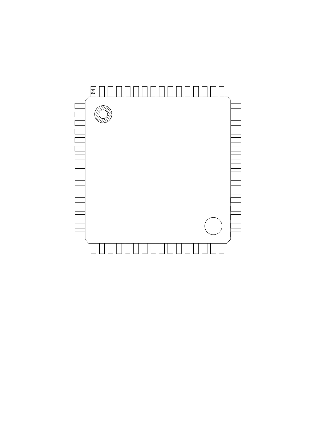
PIN CONFIGURATION (TOP VIEW)
SEG5
SEG6
SEG7
SEG8
SEG9
SEG10
SEG11
SEG12
SEG13
SEG14
SEG15
10
11
12SEG16
13SEG17
14SEG18
15SEG19
16SEG20
57
DD
V
56
DA
55
CP
54
53 CS
52 RESET
51 OSC1
50 OSC0
49 GND
48
V
FL
COM16
47
COM15
46
COM14
45
COM13
44
COM12
43
COM11
42
COM10
41
COM9
40
COM8
39
COM7
38
37 COM6
36 COM5
35 COM4
34 COM3
33 COM2
SEG4
SEG3
SEG2
SEG1
AD1
AD2P2P1
64
63
62
61
60
59
58
1
2
3
4
5
6
7
8
9
17
18
SEG21
SEG22
19
20
SEG23
SEG24
21
22
23
24
25
26
SEG25
SEG26
SEG27
SEG28
SEG29
SEG30
NC: No connection
64-Pin Plastic QFP
27
28SEG32
SEG31
29SEG33
30SEG34
31SEG35
32COM1
4/32

¡ Semiconductor ML9206-xx
P1
1
P2
2
AD2
AD1
SEG1
SEG2
SEG3
SEG4
SEG5
SEG6
SEG7
SEG8
SEG9
SEG10
SEG11
SEG12
SEG13
SEG14
SEG15
SEG16
SEG17 COM5
SEG18 COM4
SEG19 COM3
SEG20 COM2
SEG21 COM1
SEG22 SEG35
SEG23 SEG34
SEG24 SEG33
SEG25 SEG32
SEG26 SEG31
SEG27 SEG30
SEG28 SEG29
3
4
5
6
7
8
9
10
11
12
13
14
15
16
17
18
19
20
21
22
23
24
25
26
27
28
29
30
31
32
64
63
62
61
60
59
58
57
56
55
54
53
52
51
50
49
48
47
46
45
44
43
42
41
40
39
38
37
36
35
34
33
V
DD
DA
CP
CS
RESET
OSC1
OSC0
GND
V
FL
COM16
COM15
COM14
COM13
COM12
COM11
COM10
COM9
COM8
COM7
COM6
64-Pin Plastic SSOP
5/32

¡ Semiconductor ML9206-xx
PIN DESCRIPTION
Pin
QFP
1 to 31,
61 to 64
32 to 47
56
48
SSOP
Type Connects to
5 to 39 SEG1 to 35 O
40 to 55 COM1 to 16
3, 4 AD1, AD2 O59, 60
1, 2 P1, P2 O57, 58
64 V
57 GND49
56 V
DD
—
FL
63 DA I55
62 CP I54
O
Fluorescent
tube anode
electrode
Fluorescent
tube grid
electrode
Fluorescent
tube anode
electrode
LED drive
control
pins
Power
supply
Micro-
controller
Micro-
controller
DescriptionSymbol
Fluorescent display tube anode electrode drive output.
Directly connected to fluorescent display tube and a pull-down
resistor is not necessary. I
>–6 mA
OH
Fluorescent display tube grid electrode drive output.
Directly connected to fluorescent display tube and a pull-down
resistor is not necessary. I
>–30 mA
OH
Fluorescent display tube anode electrode drive output.
Directly connected to fluorescent display tube and a pull-down
resistor is not necessary. I
>–15 mA
OH
General port output.
Output of these pins in static operation, so these pins can drive
the LED.
-GND are power supplies for internal logic.
V
DD
V
Apply V
are power supplies for driving fluorescent tubes.
DD-VFL
after VDD is applied.
FL
Serial data input (positive logic).
Input from LSB.
Shift clock input.
Serial data is shifted on the rising edge of CP.
61 CS I53
Micro-
controller
Chip select input.
Serial data transfer is disabled when CS pin is "H" level.
Reset input.
"Low" initializes all the functions.
Initial status is as follows.
• Address of each RAM
Micro-
60 RESET I52
controller
or
C
, R
2
• Data of each RAM
• Display digit
• brightness adjusment
• All lights ON or OFF
2
• All outputs
RESET
address "00"H
Content is undefined
16 digits
0/256
OFF mode
"Low" level
(Circuit when R and C are
connected externally)
C
2
R
2
See Application Circuit.
External RC pin for RC oscillation.
58 OSC0 I50
Connect R and C externally. The RC time constant depends on the
VDD voltage used. Set the target oscillation frequency to 2 MHz.
C
, R
1
1
59 OSC1 O51
OSC0
OSC1
(RC oscillation circuit)
R
1
See Application Circuit.
C
1
6/32

¡ Semiconductor ML9206-xx
ABSOLUTE MAXIMUM RATINGS
Parameter
Supply Voltage (1)
Supply Voltage (2)
Input Voltage
Symbol Condition Rating Unit
V
DD
V
FL
V
IN
—
—
—
QFP
Power Dissipation
Storage Temperature
Output Current
P
D
T
STG
I
O1
I
O2
I
O3
I
O4
Ta≥25°C
—
COM1 to COM16
AD1, AD2
SEG1 to SEG35
P1, P2 –4.0 to +4.0
RECOMMENDED OPERATING CONDITIONS-1
When the power supply voltage is 5V (typ.)
Parameter
Supply Voltage (1)
Supply Voltage (2)
High Level Input Voltage
Low Level Input Voltage
CP Frequency
Oscillation Frequency
Frame Frequency
Operating Temperature
Symbol Condition Min. Typ. Max. Unit
V
V
V
V
f
f
T
DD
FL
IH
IL
f
C
OSC
FR
op
All input pins excluding OSC0 pin
All input pins excluding OSC0 pin
R
DIGIT=1 to 16, R1=3.3kW, C1=47pF
—
—
—
=3.3kW, C1=47pF
1
—
4.5
–60
0.7V
—
—
1.5
183
–40
–0.3 to +6.5
–80 to V
–0.3 to V
–55 to +150
–40 to 0.0
–20 to 0.0
–10 to 0.0
DD
541
590SSOP
5.0
—
—
—
—
2.0
244
—
DD
DD
+0.3
+0.3
5.5
–20
—
0.3V
2.0
2.5
305
+85
DD
V
V
V
mW
°C
mA
V
V
V
V
MHz
MHz
Hz
°C
7/32

¡ Semiconductor ML9206-xx
RECOMMENDED OPERATING CONDITIONS-2
When the power supply voltage is 3.3V (typ.)
Parameter
Supply Voltage (1)
Supply Voltage (2)
High Level Input Voltage
Low Level Input Voltage
CP Frequency
Oscillation Frequency
Frame Frequency
Operating Temperature
Symbol Condition Min. Typ. Max. Unit
V
V
V
V
f
OSC
f
T
f
DD
FR
—
FL
All input pins excluding OSC0 pin
IH
All input pins excluding OSC0 pin
IL
C
R
DIGIT=1 to 16, R1=3.3kW, C1=39pF
op
—
—
=3.3kW, C1=39pF
1
—
3.0
–60
0.8V
—
—
1.5
183
–40
DD
3.3
—
—
—
—
2.0
244
—
3.6
–20
—
0.2V
2.0
2.5
305
+85
ELECTRICAL CHARACTERISTICS
DC Characteristics-1
(V
=5.0V±10%, VFL=–60V, Ta=–40 to +85°C, unless otherwise specified)
DD
Parameter Symbol Applied pin Condition Min. Max. Unit
High Level Input Voltage
Low Level Input Voltage
High Level Input Current
Low Level Input Current
High Level Output
Voltage
Low Level Output
Voltage
Supply Current
V
V
V
V
V
V
V
V
I
I
IH
IL
I
IH
I
IL
OH1
OH2
OH3
OH4
OL1
OL2
DD1
DD2
CS, CP,
RESET
CS, CP,
RESET
CS, CP,
RESET
CS, CP,
RESET
COM1 to 16
AD1, AD2
SEG1 to 35
P1, P2
COM1 to 16
AD1, AD2
SEG1 to 35
P1, P2
V
DD
DA,
DA,
DA,
DA,
f
=
OSC
2MHz,
no load
—
—
V
IH=VDD
VIL=0.0V
I
=–30mA
OH1
=–15mA
I
OH2
=–6mA
I
OH3
I
=–2mA
OH4
—
I
=2mA
OL1
Duty=240/256
Digit=1 to 16
All output lights ON
Duty=128/256
Digit=1 to 9
All output lights OFF
0.7V
DD
—
0.3V
–1.0
–1.0
–1.5
V
DD
–1.5
V
DD
V
–1.5
DD
–1.0
V
DD
—VFL+1.0 V
—
—
—
DD
—
+1.0
+1.0
—
—
—
—
1.0
4
3
DD
V
V
V
V
MHz
MHz
Hz
°C
V
V
µA
µA
V
V
V
V
V
mA
mA
8/32

¡ Semiconductor ML9206-xx
DC Characteristics-2
(V
=3.3V±10%, VFL=–60V, Ta=–40 to +85°C, unless otherwise specified)
DD
Parameter Symbol Applied pin Condition Min. Max. Unit
CS, CP, DA,
High Level Input Voltage
V
IH
RESET
—
0.8V
DD
CS, CP, DA,
Low Level Input Voltage
V
IL
RESET
—
—
0.2V
CS, CP, DA,
High Level Input Current
I
IH
RESET
V
IH=VDD
–1.0
CS, CP, DA,
Low Level Input Current
High Level Output
Voltage
V
V
V
V
I
IL
OH1
OH2
OH3
OH4
RESET
COM1 to 16
AD1, AD2
SEG1 to 35
P1, P2
VIL=0.0V
I
=–30mA
OH1
=–15mA
I
OH2
=–6mA
I
OH3
I
=–1mA
OH4
V
V
V
V
–1.0
DD
DD
DD
DD
–1.5
–1.5
–1.5
–1.0
COM1 to 16
Low Level Output
Voltage
V
OL1
V
OL2
AD1, AD2
SEG1 to 35
P1, P2
I
OL1
—
=1mA
—VFL+1.0 V
—
Duty=240/256
Digit=1 to 16
=
All output lights ON
Duty=128/256
Digit=1 to 9
—
—
Supply Current
I
I
DD1
DD2
f
OSC
V
DD
2MHz,
no load
All output lights OFF
—
+1.0
+1.0
—
—
—
—
1.0
3
2
DD
V
V
µA
µA
V
V
V
V
V
mA
mA
9/32

¡ Semiconductor ML9206-xx
AC Characteristics-1
(V
=5.0V±10%, VFL=–60V, Ta=–40 to +85°C, unless otherwise specified)
DD
Parameter Symbol Condition Min. Max. Unit
CP Frequency f
CP Pulse Width
DA Setup Time
DA Hold Time
CS Setup Time
CS Hold Time
CS Wait Time
Data Processing Time
RESET Pulse Width
t
t
t
RESET Time t
DA Wait Time
t
RSOFF
All Output Slew Rate
V
Rise Time
DD
VDD Off Time t
C
t
CW
t
DS
t
DH
t
CSS
t
CSH
CSW
DOFF
WRES
RSON
t
R
t
F
t
PRZ
POF
R
1
R
1
When RESET signal is input from
microcontroller etc. externally
When RESET signal is input from
microcontroller etc. externally
R2=1.0kW, C2=0.1mF — 200 ms
Cl=100pF
When mounted in the unit
When mounted in the unit, VDD=0.0V 5.0 — ms
— — 2.0 MHz
—
—
—
—
=3.3kW, C1=47pF
—
=3.3kW, C1=47pF
250
250
250
250
16
250
8
250 — ns
250 — ns
—
t
R
=80% to 20%
t
F
=20% to 80%
250
—
— 2.0 ms
—
—
—
—
—
—
—
—
—
2.0
100
ns
ns
ns
ns
ms
ns
ms
ns
ms
ms
AC Characteristics-2
Parameter Symbol Condition Min. Max. Unit
CP Frequency f
CP Pulse Width
DA Setup Time
DA Hold Time
CS Setup Time
CS Hold Time
CS Wait Time
Data Processing Time
RESET Pulse Width
RESET Time t
DA Wait Time
All Output Slew Rate
V
Rise Time
DD
VDD Off Time t
t
CW
t
DS
t
DH
t
CSS
t
CSH
t
CSW
t
DOFF
t
WRES
RSON
t
RSOFF
t
R
t
t
PRZ
POF
=3.3V±10%, VFL=–60V, Ta=–40 to +85°C, unless otherwise specified)
(V
DD
C
R
R
When RESET signal is input from
microcontroller etc. externally
When RESET signal is input from
microcontroller etc. externally
— — 2.0 MHz
—
—
—
—
=3.3kW, C1=39pF
1
—
=3.3kW, C1=39pF
1
250
250
250
250
16
250
8
250 — ns
250 — ns
R2=1.0kW, C2=0.1mF — 200 ms
—
tR=20% to 80%
C
=100pF
F
l
t
=80% to 20%
F
When mounted in the unit
250
—
— 2.0 ms
—
When mounted in the unit, VDD=0.0V 5.0 — ms
—
—
—
—
—
—
—
—
2.0
100
ns
ns
ns
ns
ms
ns
ms
ns
ms
ms
10/32
 Loading...