

OKI ML9044CVWA Datasheet

E2B0055-19-61
Preliminary
¡ Semiconductor ML9044
This version: Jun. 1999
¡ Semiconductor
ML9044
DOT MATRIX LCD CONTROLLER DRIVER
GENERAL DESCRIPTION
The ML9044 used in combination with an 8–bit or 4–bit microcontroller controls the operation
of a character type dot matrix LCD.
FEATURES
• Easy interfacing with 8–bit or 4–bit microcontroller
• Switchable between serial and parallel interfaces
• Dot–matrix LCD controller/driver for a small (5 ¥ 7 dots) or large (5 ¥ 10 dots) font
• Built–in circuit allowing automatic resetting at power–on
• Built–in 17 common signal drivers and 120 segment signal drivers
• Built–in character generation ROM capable of generating 160 small characters (5 ¥ 7 dots) or
32 large characters (5 ¥ 10 dots)
• Creation of character patterns by programming: up to 8 small character patterns (5 ¥ 8 dots) or
up to 4 large character patterns (5 ¥ 11 dots)
• Built–in RC oscillation circuit using external or internal resistors
• Program–selectable duties: 1/9 duty (1 line: 5 ¥ 7 dots + cursor + arbitrator), 1/12 duty (1 line:
5 ¥ 10 dots + cursor + arbitrator), or 1/17 duty (2 lines: 5 ¥ 7 dots + cursor + arbitrator)
• Built–in bias dividing resistors to drive the LCD
• Bi–directional transfer of segment outputs
• Bi–directional transfer of common outputs
• Equipped with a 120–dot arbitrator
• Display shifting on each line
• Built–in contrast control circuit
• Built–in voltage multiplier circuit
• Chip (Gold Bump) Product name : ML9044CVWA
1/54

¡ Semiconductor ML9044
2/54
BLOCK DIAGRAM
V
DD
GND
OSC
1
OSC
R
OSC
2
RS1
RS0
R/W
E
CS
P/S
SHT
SI
SO
DB
0
to
DB
3
4
DB
4
to
DB
7
4
T
1
T
2
T
3
V
1
V
2
V
3B
V
3A
V
4
V
5
V
5IN
Timing
generator
8
I/O
buffer
8
Instruction
register
(IR)
Instruction
decoder
(ID)
7
8
8
8
Data
register
(DR)
5
COM
1
SEG
1
COM
17
Test
circuit
LCD
bias
voltage
dividing
circuit
5
8
Busy flag
(BF)
Expansion
Instruction
register (ER)
Voltage
multiplier
circuit
Address
counter
(ADC)
Expansion
Instruction
decoder (ED)
Character
generator
ROM
(CGROM)
8
8
Display
data RAM
(DDRAM)
Arbitrator
RAM
(ABRAM)
Character
generator
RAM
(CGRAM)
Cursor
blink
controller
5
5
CSR
17-bit
shift
register
Common
signal
driver
Rarallel-
serial
converter
120-bit shift register
120-bit latch
Segment Signa - driver
SEG
120
SSR
BEB
VCCVCV
IN
¡ Semiconductor ML9044
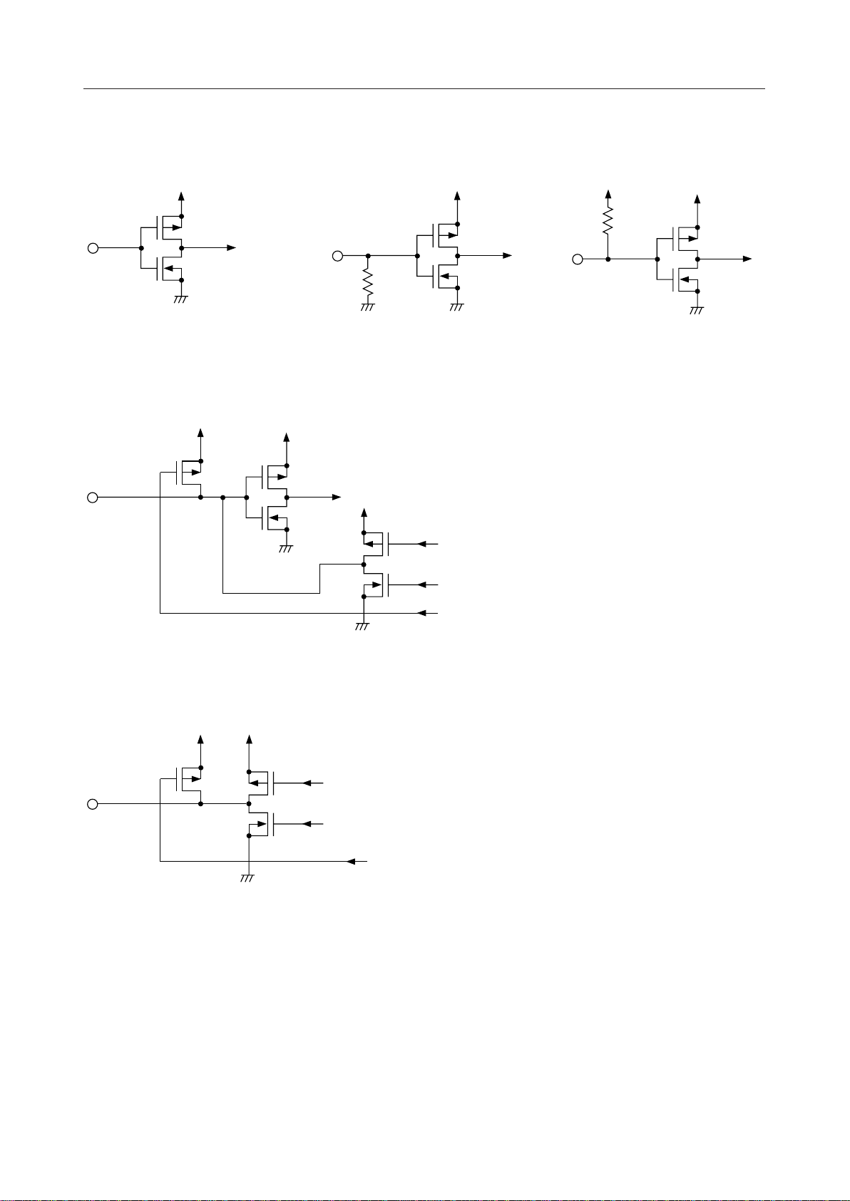
I/O CIRCUITS
V
DD
P
N
Applied to pins E, SSR, CSR, BEB, CS
P/S, SHT, and SI
V
DD
V
DD
P
V
DD
P
N
Applied to pins T1, T2, and T
3
V
DD
V
DD
P
N
Applied to pins R/W, RS1, and RS
0
P
V
DD
N
P
V
DD
Applied to pins DB0 to DB7
V
DD
PP
N
Applied to pins SO
N
Output Enable signal
Output Enable signal
3/54
¡ Semiconductor ML9044
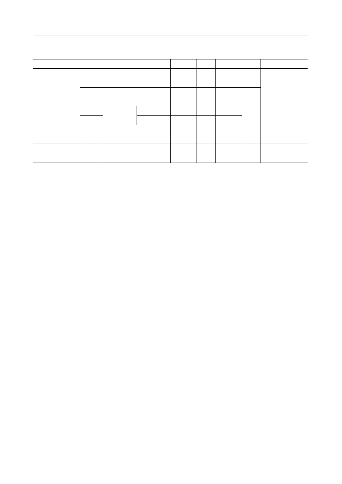
PIN DESCRIPTIONS
Symbol Description
R/W
RS0, RS
1
E
DB0 to DB
DB4 to DB
OSC
1
OSC
2
OSC
R
COM1 to COM
SEG1 to SEG
3
7
17
120
The input pin with a pull–up resistor to select Read (“H”) or Write (“L”) in the Parallel
I/F Mode.
This pin should be open in the Serial I/F Mode.
The input pins with a pull–up resistor– to select a register in the Parallel I/F Mode.
RS
1
RS
0
Name of register
H H Data register
H L Instruction register
L L Expansion Instruction register
This pin should be open in the Serial I/F Mode.
The input pin for data input/output between the CPU and the ML9044 and for activating
instructions in the Parallel I/F Mode.
This pin should be open in the Serial I/F Mode.
The input/output pins to transfer data of lower–order 4 bits between the CPU and the
ML9044 in the Parallel I/F Mode. Each pin is equipped with a pull–up resistor. These 4
lines are not used for the 4–bit interface.
This pin should be open in the Serial I/F Mode.
The input/output pins to transfer data of upper 4 bits between the CPU and the ML9044
in the Parallel I/F Mode. Each pin is equipped with a pull–up resistor.
This pin should be open in the Serial I/F Mode.
The clock oscillation pins required for LCD drive signals and the operation of the
ML9044 by instructions sent from the CPU.
To input external clock, the OSC
pin should be used. The OSCR and the OSC2 pins
1
should be open.
To start oscillation with an external resistor, the resistor should be connected between
the OSC
To start oscillation with an internal resistor, the OSC
short–circuited outside the ML9044. The OSC
and OSC2 pins. The OSCR pin should be open.
1
2
pin should be open.
1
and OSCR pins should be
The LCD common signal output pins.
For 1/9 duty, non–selectable voltage waveforms are output via COM
1/12 duty, non–selectable voltage waveforms are output via COM
to COM17. For
10
to COM17.
13
The LCD segment signal output pins.
4/54

¡ Semiconductor ML9044
Symbol Description
CSR
The input pin to select the transfer direction of the common signal output data.
Refer to the Expansion Instruction Codes section about the AS bit.
CSR duty AS bit shift direction arbitrator's common pin
L 1/9 L COM1 Æ COM9 COM9
L 1/9 H COM2 Æ COM9, COM1 COM1
L 1/12 L COM1 Æ COM12 COM12
L 1/12 H COM2 Æ COM12, COM1 COM1
L 1/17 L COM1 Æ COM17 COM17
L 1/17 H COM2 Æ COM17, COM1 COM1
H 1/9 L COM9 Æ COM1 COM1
H 1/9 H COM8 Æ COM1, COM9 COM9
H 1/12 L COM12 Æ COM1 COM1
H 1/12 H COM11 Æ COM1, COM12 COM12
H 1/17 L COM17 Æ COM1 COM1
H 1/17 H COM16 Æ COM1, COM17 COM17
SSR
V1, V2, V3A, V3B, V
BEB
V
IN
V5, V
5IN
The input pin to select the transfer direction of the segment signal output data.
“L”: Data transfer from SEG
“H”: Data transfer from SEG
The pins to output bias voltages to the LCD.
4
For 1/4 bias : The V
For 1/5 bias : The V
and V3B pins are shorted.
2
3A
to SEG
1
120
120
to SEG
1
and V3B pins are shorted.
The input pin to enable or disable the voltage multiplier circuit.
“L” disables the voltage multiplier circuit. “H” enables the voltage multiplier circuit.
The voltage multiplier circuit doubles the input voltage V
and outputs it to the V
IN
The voltage multiplier circuit can be used only when generating a level lower than GND.
The pin to input voltage to the voltage multiplier.
The pins to supply the LCD drive voltage.
The LCD drive voltage is supplied to the V
pin when the voltage multiplier is not used
5
(BEB = 0) and the internal contrast adjusting circuit is also not used. At this time, the
V
pin should be open.
5IN
The LCD drive voltage is supplied to the V
pin when the voltage multiplier is not used
5IN
(BEB = 0) but the internal contrast adjusting circuit is used. At this time, the V
should be open.
When the voltage multiplier is used (BEB = 1), the V
multiplied voltage is output to the V
pin). In this case, the internal contrast adjusting
5IN
and V5 pins should be open (the
5IN
circuit is used automatically.
pin
5
5IN
pin.
V
C
V
CC
The pin to connect the positive pin of the capacitor for the voltage multiplier.
The pin to connect the negative pin of the capacitor used for the voltage multiplier.
5/54

¡ Semiconductor ML9044
Symbol Description
T1, T2, T
V
DD
GND
P/S
CS
SHT
3
The input pins for test circuits (normally open). Equipped with a pull–down resistor.
The power supply pin.
The ground level input pin.
The input pin to select the parallel or serial interface.
“L” selects the parallel interface.
“H” selects the serial interface.
The pin to enable this IC in the serial I/F mode.
“L” enables this IC.
“H” disables this IC.
This pin should be open in the parallel I/F mode.
The pin to input shift clock in the serial I/F mode.
Data inputting to the SI pin is carried out synchronizing with the rising edge of this
clock signal.
Data outputting from the SO pin is carried out synchronizing with the falling edge of this
clock signal.
This pin should be open in the parallel I/F mode.
SI
SO
The pin to input DATA in the serial I/F mode.
Data inputting to this pin is carried out synchronizing with the rising edge of the SHT
signal.
This pin should be open in the parallel I/F mode.
The pin to output DATA in the serial I/F mode.
Data inputting to this pin is carried out synchronizing with the falling edge of the SHT
signal.
This pin should be open in the parallel I/F mode.
6/54
¡ Semiconductor ML9044
ABSOLUTE MAXIMUM RATINGS
Parameter Symbol Condition Rating Unit Applicable pins
Supply Voltage V
, V2, V3,
V
LCD Driving Voltage
1
V
4
Input Voltage V
Storage Temperature T
DD
, V
STG
5
I
Ta = 25°C –0.3 to +6.5 V VDD – GND
Ta = 25°C VDD – 7.5 to VDD+0.3 V
Ta = 25°C –0.3 to VDD+0.3 V
— –55 to +125 °C —
RECOMMENDED OPERATING CONDITIONS
Parameter Symbol Condition Range Unit Applicable pins
Supply Voltage V
VDD–V
LCD Driving Voltage
(See Note)
Input Voltage V
Operating Temperature T
DD
5
IN
op
— 2.5 to 5.5 V VDD–GND
— 2.8 to 7.0 V
BEB = 1
— –40 to +85 °C —
V
DD
V
–1.40 to
–3.5
DD
(GND = 0V)
V
, V4, V5, V
1
, V3A, V
V
2
3B
5IN
,
R/W, E, SHT, CSR,
P/S, SSR, SI, RS
, BEB, CS,
RS
1
to T3, DB0 to DB7,
T
1
V
IN
0
(GND = 0V)
V
DD–V5
(V
)
5
IN
VV
DD–VIN
,
Note: This voltage should be applied across VDD and V5. The following voltages are output
to the V1, V2, V3A (V3B) and V4 pins:
• 1/4 bias
V1 = {VDD–(VDD–V
V2 = V3B= {VDD–(VDD–V
V4 = {VDD–3 ¥ (VDD–V
)/4} ±0.15V
5
)/2} ±0.15V
5
)/4 } ±0.15V
5
• 1/5 bias
V1 = {VDD–(VDD–V
V2 = {VDD–2 ¥ (VDD–V
V3A = V3B= {VDD–3 ¥ (VDD–V
V4 = {VDD–4 ¥ (VDD–V
)/5} ±0.15V
5
)/5} ±0.15V
5
)/5} ±0.15V
5
)/5} ±0.15V
5
The voltages at the V1, V2, V3A (V3B), V4 and V5 pins should satisfy
VDD>V1>V2>V3A(V3B)>V4>V5.
(Higher ¨Æ Lower)
* Do not apply short–circuiting across output pins and across an output pin and an
input/output pin or the power supply pin in the output mode.
7/54
¡ Semiconductor ML9044
ELECTRICAL CHARACTERISTICS
DC Characteristics
(GND = 0V, VDD = 2.5V to 5.5V, Ta = –40 to +85°C)
Parameter Symbol Condition Min Typ Max Unit Applicable pin
“H” Input Voltage 1
“L” Input Voltage 1
V
IH1
V
IL1
— 0.8V
–0.3 — 0.2V
—VDDV
DD
DD
R/W, RS0, RS1,
E, DB
to DB
0
SHT, P/S, SI, CS
“H” Input Voltage 2
“L” Input Voltage 2
“H” Output Voltage 1
“L” Output Voltage 1
“H” Output Voltage 2
“L” Output Voltage 2
COM Voltage
Drop
SEG Voltage
Drop
Input Leakage
V
IH2
V
IL2
V
OH1IOH
V
OL1IOL
V
OH2IOH
V
OL2IOL
V
CHIOCH
V
CMHIOCMH
V
CMLIOCML
V
CLIOCL
V
SHIOSH
V
SMHIOSMH
V
SMLIOSML
V
SLIOSL
| IIL |
VDD = 5V, VIN = 5V or 0V
= –0.1mA 0.75V
= +0.1mA — — 0.2V
= –13mA 0.9V
= +13mA — — 0.1V
= –4mAV
= +4mAV
= –4mAV
= +4mA
Current
Input Current 1 | II1| VDD =
VDD =
— 0.8V
VDD –V5 = 5V
= ±4mA
= ±4mA
V
– V5 = 5V
DD
= ±4mA
= ±4mA
5V, V
=
GND 10 25 61 mA
I
N
5V, V
=
VDD,
I
N
Note 1
Note 1
—VDDV
DD
–0.3 — 0.2V
—— V
DD
—— V
DD
– 0.3 V
DD
DD
DD
DD
DD
V1 – 0.3 V1 + 0.3
V4 – 0.3 V4 + 0.3
5
– 0.3 V
DD
V5 + 0.3
DD
V2 – 0.3 V2 + 0.3
V3 – 0.3 V3 + 0.3
V
5
V5 + 0.3
— — 1.0 mA
— — 2.0
OSC
SSR, CSR, BEB
DB
0
OSC
V
COM1 to COM
V
SEG1 to SEG
E, SSR, CSR, BEB,
SHT, P/S, CS, SI
R/W, RS0, RS
DB0 to DB7, SO
,
1
to DB7, SO
2
Excluding current flowing
through the pull-up resistor
and the output driving MOS
Input Current 2 | II2| VDD =
VDD =
5V, V
5V, V
=
V
I
N
DD
=
VDD,
I
N
15 45 105 mA
— — 2.0
T
1
, T2, T
Excluding current flowing
through the pull-down resistor
Supply Current I
LCD Bias Resistor
VDD = 5V Note 2
DD
R
LB
— — 1.2 mA
4.0 kW
VDD – GND
V
, V1, V
DD
V3A, V3B, V4, V
Oscillation Frequency of
External Resistor Rf
Oscillation Frequency of
Internal Resistor Rf
Clock Input
Frequency
Input Clock Duty
Input Clock Rise Time
External Clock
Input Clock Fall Time
f
f
f
Rf = 120kW±2% Note 3
osc1
OSC1: Open
osc2
OSC2 and OSCR: Short-circuited
OSC2, OSCR: Open
f
in
Input from OSC
duty
f
rf
f
ff
175 270 350 kHz
Note 4
140 270 480 kHz
125 480 kHz
1
Note 5 45 50 55 %
Note 6 — — 0.2 mS
Note 6 — — 0.2 mS
OSC1, OSC
OSC1, OSC2,
OSC
R
OSC
1
7
17
120
1
3
2
5
2
8/54
¡ Semiconductor ML9044
(GND = 0V, VDD = 2.5V to 5.5V, Ta = –40 to +85°C)
Parameter Symbol Condition Min Typ Max Unit Applicable pin
Control Range of
LCD Driving
Voltage (by internal
variable resistor)
Bias Voltage for Driving
LCD by External Input
Voltage Multiplier
Output Voltage
Voltage Multipler
Input Voltage
V
LCD
MAX
V
LCD
MIN
V
LCD1VDD
V
LCD2
V5OUT VDD = 3V, VIN = 0V
V
IN
= 5V, 1/5 bias
V
DD
V
= 0V
5IN
V
= 5V, 1/5 bias
DD
= 0V
V
5IN
– V5 2.8 — 7.0 V
Note 7
1/5
bias
1/4
bias 2.8 — 7.0
BEB = H
TBD —
VDD –
2VIN—
— TBD
VDD –2V
+1.2V
VDD/2 V
– V
V
DD
5
V
5
V
IN
V5, V
V
IN
5IN
9/54
¡ Semiconductor ML9044
Note 1: Applied to the voltage drop occurring between any of the VDD, V1, V4 and V5 pins and
any of the common pins (COM1 to COM17) when the current of 4mA flows in or flows
out at one common pin.
Also applied to the voltage drop occurring between any of the VDD, V2, V3A (V3B) and
V5 pins and any of the segment pins (SEG1 to SEG
) when the current of 4mA flows
120
in or flows out at one common pin.
The current of 4mA flows out when the output level is VDD or flows in when the output
level is V5.
Note 2: Applied to the current flowing into the VDD pin when the external clock (f
270 kHz) is fed to the internal Rf oscillation or OSC1 under the following conditions:
VDD = 5V
GND = V5 = 0V,
V1, V2, V3A (V3B) and V4: Open
E, SSR, CSR, and BEB: “L” (fixed)
Other input pins: “L” or “H” (fixed)
Other output pins: No load
Note 3: Note 4:
OSC
1
OSC
OSC
OSC
1
R
= 120kW±2%
R
2
f
OSC
OSC
R
2
osc2
= fin =
The wire between OSC1 and Rf and the wire between
and Rf should be as short as possible.
OSC
2
Keep OSC
open.
R
Note 5:
V
DD
2
f
IN
waveform
The wire between OSC2 and OSCR should be as short
as possible. Keep OSC
t
HW
V
DD
2
t
LW
open.
1
V
DD
2
Applied to the pulses entering from the OSC1 pin
f
= tHW/ (tHW + tLW) ¥ 100 (%)
duty
10/54
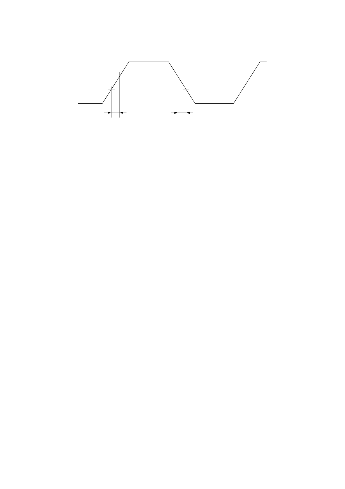
¡ Semiconductor ML9044
Note 6:
0.3V
0.7V
DD
DD
t
rf
t
0.7V
ff
DD
0.3V
DD
Applied to the pulses entering from the OSC1 pin
Note 7: For 1/4 bias, V2 and V3B pins are short–circuited. V3A pin is open.
For 1/5 bias, V3A and V3B pins are short–circuited. V2 pin is open.
11/54

¡ Semiconductor ML9044
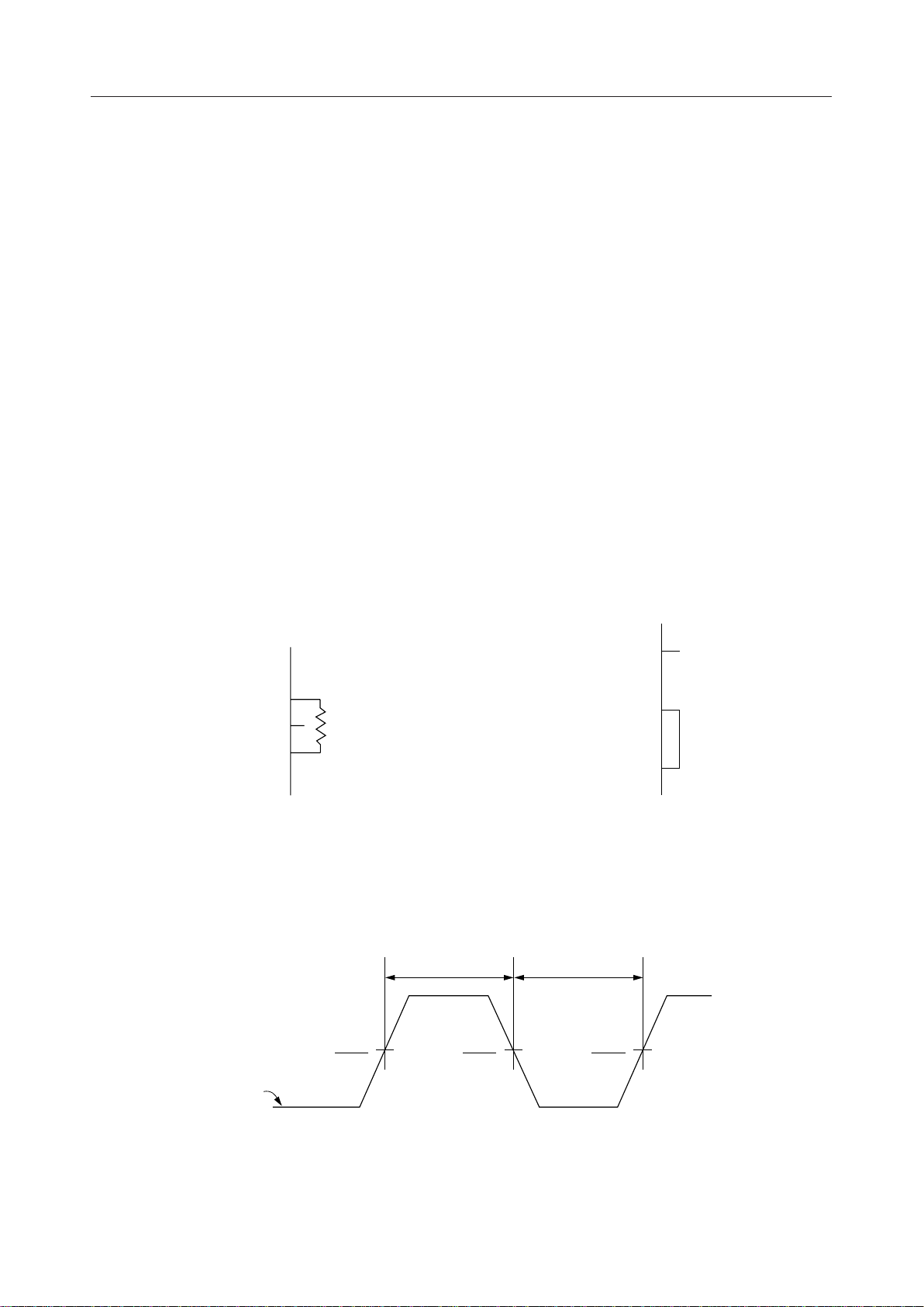
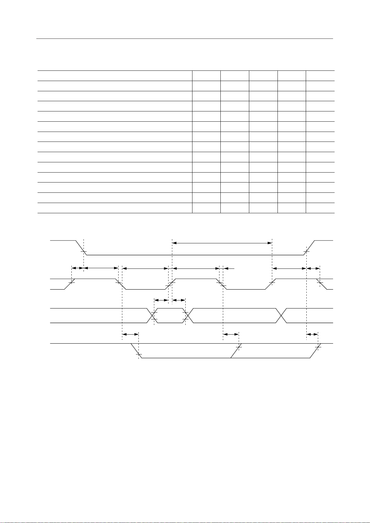
Switching Characteristics (The following ratings are subject to change after ES evaluation.)
• Parallel Interface Mode
The timing for the input from the CPU (see 1) and the timing for the output to the CPU (see 2)
are as shown below:
1) WRITE MODE (Timing for input from the CPU)
(VDD = 2.5 to 5.5V, Ta = –40 to +85°C)
Parameter Symbol UnitMin Typ Max
R/W, RS
, RS1 Setup time 40 — —t
0
E Pulse Width 450 — —t
R/W, RS
, RS1 Hold time 10 — —t
0
E Rise Time — — 25t
E Fall Time — — 25t
E Pulse Width 430 — —t
E Cycle Time 1000 — —t
to DB7 Input Data Hold time 195 — —t
DB
0
to DB7 Input Data Setup time 10 — —t
DB
0
B
W
A
r
f
L
C
I
H
ns
ns
ns
ns
ns
ns
ns
ns
ns
DB
RS1, RS
R/W
to DB
0
V
0
E
7
V
IL
IH
V
IL
V
IL
t
t
B
t
L
V
IL
r
V
IH
t
c
t
W
t
I
V
V
Input
IH
Data
IL
V
IH
V
IL
V
IL
t
f
V
IH
t
A
V
IL
t
H
V
IH
V
IL
12/54

¡ Semiconductor ML9044
2) READ MODE (Timing for output to the CPU)
(VDD = 2.5 to 5.5V, Ta = –40 to +85°C)
Parameter Symbol UnitMin Typ Max
R/W, RS
, RS0 Setup Time 40 — —t
1
E Pulse Width 450 — —t
R/W, RS
, RS0 Hold Time 10 — —t
1
E Rise Time — — 25t
E Fall Time — — 25t
E Pulse Width 430 — —t
E Cycle Time 1000 — —t
to DB7 Output Data Delay Time — — 350t
DB
0
to DB7 Output Data Hold Time 20 — —t
DB
0
B
W
A
r
f
L
C
D
O
ns
ns
ns
ns
ns
ns
ns
ns
ns
DB
0
RS
to
1, 0
R/W
E
DB
V
IH
V
IL
V
IH
t
t
B
t
L
V
IL
7
V
IL
r
V
IH
t
D
t
c
t
W
V
V
OH
OL
Output
Data
V
IH
V
IL
V
IH
t
f
V
IH
t
A
V
IL
t
O
V
OH
V
OL
13/54
¡ Semiconductor ML9044
• Serial Interface Mode
(VDD = 2.5 to 5.5V, Ta = –40 to +85°C)
Parameter Symbol UnitMin Typ Max
SHT Cycle Time 500 — —t
CS Setup Time 100 — —t
CS Hold Time 100 — —t
SHT Setup Time 60 — —t
SHT Hold Time 200 — —t
SHT "H" Pulse Width 200 — —t
SHT "L" Pulse Width 200 — —t
SHT Rise Time — — 50t
SHT Fall Time — — 50t
SI Setup Time 100 — —t
SI Hold Time 100 — —t
Data Output Delay Time — — 160t
Data Output Hold Time 0 — —t
SCY
CSU
CH
SSU
SH
SWH
SWL
SR
SF
DISU
DIH
DOD
CDH
ns
ns
ns
ns
ns
ns
ns
ns
ns
ns
ns
ns
ns
CS
SHT
SI
SO
t
CSU
t
SCY
V
IL
t
SSU
V
IH
t
DOD
t
SWL
V
IH
V
IL
V
V
IL
t
DISUtDIH
OL
t
SR
t
SWH
V
IH
V
IH
V
IL
t
SF
V
V
IH
t
DOD
IL
V
OH
t
SH
V
IH
t
CDH
t
CH
V
OH
14/54

¡ Semiconductor ML9044
FUNCTIONAL DESCRIPTION
Instruction Register (IR), Data Register (DR), and Expansion Instruction Register (ER)
These registers are selected by setting the level of the Register Selection input pins RS0 and RS1.
The DR is selected when both RS0 and RS1 are “H”. The IR is selected when RS0 is “L” and RS
is “H”. The ER is selected when both RS0 and RS1 are “L”. (When RS0 is “H” and RS1 is “L”, the
ML9044 is not selected.)
The IR stores an instruction code and the address code of the display data RAM (DDRAM) or the
character generator RAM (CGRAM).
The microcontroller (CPU) can write to the IR but cannot read from the IR.
The ER stores a contrast adjusting code and the address code of the arbitrator RAM (ABRAM).
The CPU can write to or read from the ER.
The DR stores data to be written in the DDRAM, ABRAM and CGRAM and also stores data read
from the DDRAM, AMRAM and CGRAM.
The data written in the DR by the CPU is automatically written in the DDRAM, ABRAM or
CGRAM.
When an address code is written in the IR or ER, the data of the specified address is automatically
transferred from the DDRAM, ABRAM or CGRAM to the DR. The data of the DDRAM, ABRAM
and CGRAM can be checked by allowing the CPU to read the data stored in the DR.
After the CPU writes data in the DR, the data of the next address in the DDRAM, ABRAM or
CGRAM is selected to be ready for the next writing by the CPU. Similarly, after the CPU reads
the data in the DR, the data of the next address in the DDRAM, ABRAM or CGRAM is set in the
DR to be ready for the next reading by the CPU.
Writing in or reading from these 3 registers is controlled by changing the status of the R/
W(Read/Write) pin.
1
Table 1 R/W pin status and register operation
R/W RS
LLH
HLH
LHH
HHH
LLL
HLL
RS
0
1
Writing in the IR
Reading the Busy flag (BF) and the address counter (ADC)
Writing in the DR
Reading from the DR
Writing in the ER
Reading the contrast code
Operation
Busy Flag (BF)
The status “1” of the Busy Flag (BF) indicates that the ML9044 is carrying out internal operation.
When the BF is “1”, any new instruction is ignored.
When R/W = “H”, RS0 = “L” and RS1 = “H”, the data in the BF is output to the DB7.
New instructions should be input when the BF is “0”.
When the BF is “1”, the output code of the address counter (ADC) is undefined.
15/54

¡ Semiconductor ML9044
Address Counter (ADC)
The address counter provides a read/write address for the DDRAM, ABRAM or CGRAM and
also provides a cursor display address.
When an instruction code specifying DDRAM, ABRAM or CGRAM address setting is input to
the pre–defined register, the register selects the specified DDRAM, ABRAM or CGRAM and
transfers the address code to the ADC. The address data in the ADC is automatically incremented
(or decremented) by 1 after the display data is written in or read from the DDRAM, ABRAM or
CGRAM.
The data in the ADC is output to DB0 to DB6 when R/W = “H”, RS0 = “L”, RS1 = “H” and BF =
“0”.
Timing Generator
The timing generator generates timing signals for the internal operation of the ML9044 activated
by the instruction sent from the CPU or for the operation of the internal circuits of the ML9041
such as DDRAM, ABRAM, CGRAM and CGROM. Timing signals are generated so that the
internal operation carried out for LCD displaying will not be interfered by the internal operation
initiated by accessing from the CPU. For example, when the CPU writes data in the DDRAM,
the display of the LCD not corresponding to the written data is not affected.
16/54
¡ Semiconductor ML9044
Display Data RAM (DDRAM)
This RAM stores the display data represented in 8–bit character coding (see Table 2).
The DDRAM addresses correspond to the display positions (digits) of the LCD as shown below.
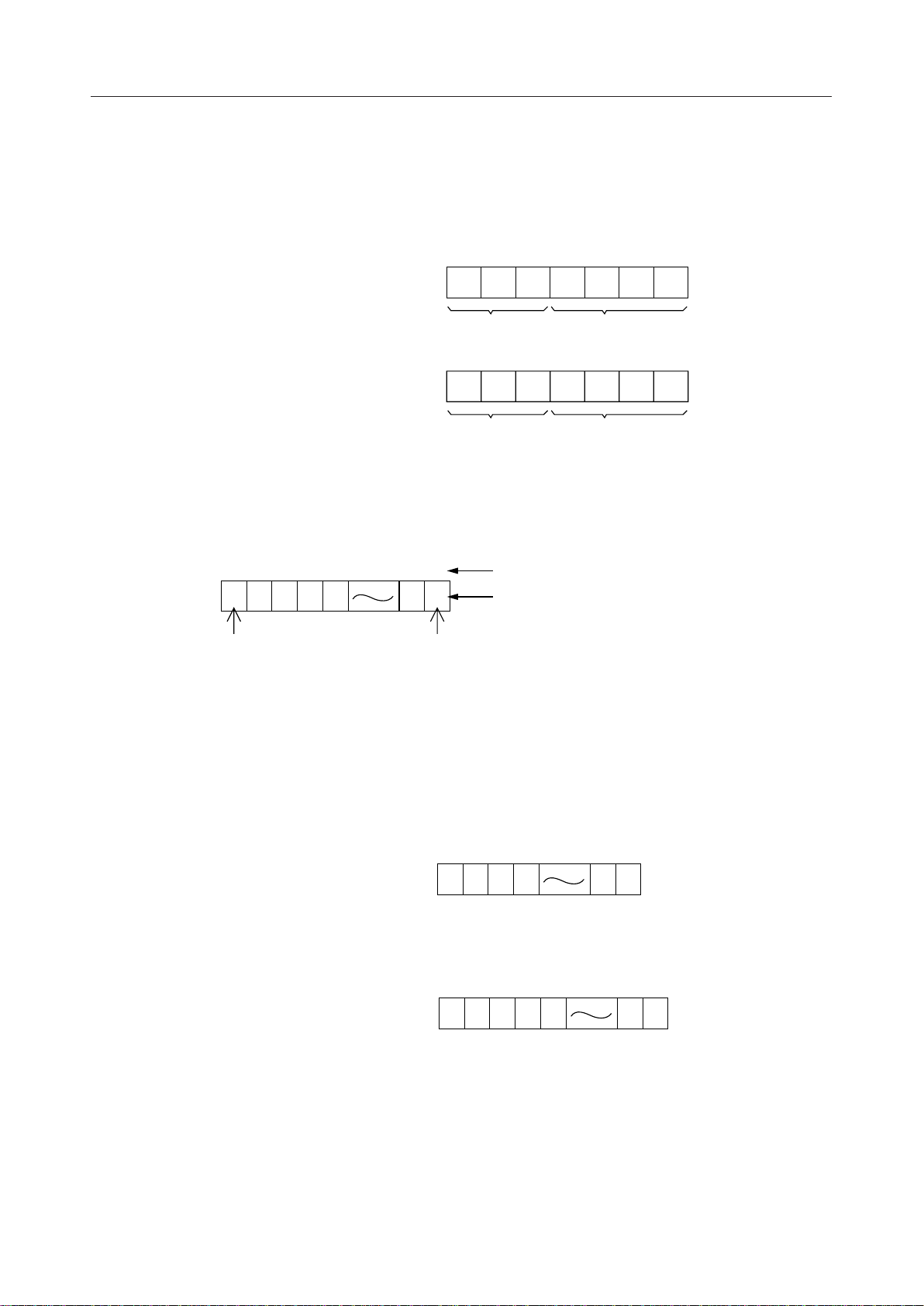
The DDRAM addresses (to be set in the ADC) are represented in hexadecimal.
DB6DB5DB4DB3DB2DB1DB
ADC
(Example) Representation of DDRAM address = 12
MSB LSB
Hexadecimal Hexadecimal
0ADC 0 1 0 0 1 0
1
2
0
1) Relationship between DDRAM addresses and display positions (1–line display mode)
Digit
1
2 3 4 5 23 24
00 01 02 03 04 16 17
Left
end
Right
end
Display position
DD RAM address (hexadecimal)
In the 1–line display mode, the ML9044 can display up to 24 characters from digit 1 to digit 24.
While the DDRAM has addresses “00” to “4F” for up to 80 character codes, the area not used for
display can be used as a RAM area for general data. When the display is shifted by instruction,
the relationship between the LCD display and the DDRAM address changes as shown below:
(Display shifted to the right)
(Display shifted to the left)
Digit
234 2324
1
4F 00 01 02 15 16
Digit
1
234
01 02 03 04 17 18
52324
05
17/54
 Loading...