

OKI ML9040 User Manual

E2B0048-29-21
Prelim
This version: Feb. 1999
ML9040-Axx/-Bxx¡ Semiconductor
¡ Semiconductor
Previous version: Mar. 1996
ML9040-Axx/-Bxx
DOT MATRIX LCD CONTROLLER WITH 16-DOT COMMON DRIVER AND 40-DOT
SEGMENT DRIVER
GENERAL DESCRIPTION
The ML9040-Axx/-Bxx is a dot matrix LCD controller which is fabricated in low power CMOS
silicon gate technology. Character display on the dot matrix character type LCD can be
controlled in combination with a 4-bit or 8-bit microcontroller. This LSI consists of 16-dot
COMMON driver, 40-dot SEGMENT driver, display data RAM, character generator RAM,
character generator ROM and control circuit.
The ML9040-Axx/-Bxx has the character generator ROM that can be programmed by custom
mask. The ML9040-Axx/-Bxx is a standard version having 160 characters with lowercase (5 x
7 dots), and 32 characters with uppercase (5 x 10 dots) in this ROM.
FEATURES
inary
• Easy interface with an 8-bit or 4-bit microcontroller.
• Dot matrix LCD controller/driver for lowercase (5 x 7 dots) or uppercase (5 x 10 dots).
• Automatic power ON reset.
• COMMON signal drivers (16) and SEGMENT signal drivers (40).
• Can control up to 80 characters when used in combination with MSM5259.
• Character generator ROM for 160 characters with lowercase (5 x 7 dots) and 32 characters with
uppercase (5 x 10 dots).
• Character patterns are programmable by character generator RAM. (Lowercase: 5 x 8 dots,
8 patterns, uppercase: 5 x 11 dots, 4 patterns).
• Built-in oscillation circuit to connect with external resistor or ceralock.
• 1/8 duty (1 line; 5 x 7 dots + cursor), 1/11 duty (1 line; 5 x 10 dots + cursor), or 1/16 duty (2
lines; 5 x 7 dots + cursor), selectable.
• Clear display even at 1/5 bias, 3.0V LCD driving voltage.
• LCD driving waveform
ML9040-Axx: A mode
ML9040-Bxx: B mode
• Package options:
80-pin plastic QFP (QFP80-P-1420-0.80-BK)
(Product name: ML9040-Axx/-BxxGA)
xx indicates code number.
1
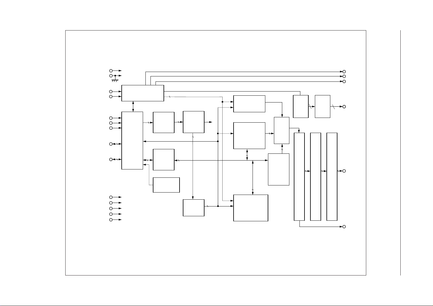
2
V
DD
GND
OSC
OSC
E
RS
R/W
DB
- DB
0
DB4 - DB
Input/
output
buffer
Timing
generation
circuit
8
8
Instruction
register
(IR)
Data
register
(DR)
Busy flag
(BF)
7
Instruction
8
decoder
(ID)
7
8
Address
counter
(ADC)
77
Cursor blink
control
Character
generator
RAM
(CG RAM)
8
Display data
RAM
(DD RAM)
16-bit
shift
register
Parallel/
serial
55
conversion
5
Character
generator
ROM
(CG RAM)
8
40-bit
shift
register
16
40-bit
latch
Common
signal
driver
4040
Segment
signal
driver
1
2
4
3
4
7
V
1
V
2
V
3
V
4
V
5
L
CP
DF
16
COM
1~16
40
SEG
1~40
DO
BLOCK DIAGRAM
¡ SemiconductorML9040-Axx/-Bxx

INPUT AND OUTPUT CONFIGURATION
V
DD
ML9040-Axx/-Bxx¡ Semiconductor
V
DD
V
DD
P
N
Applicable to pin E.
V
DD
V
DD
P
N
Applicable to pins DB
V
DD
- DB7.
0
P
N
Applicable to pins R/W and RS.
P
V
DD
N
P
N
Applicable to pins DO, CP, L, and DF.
3
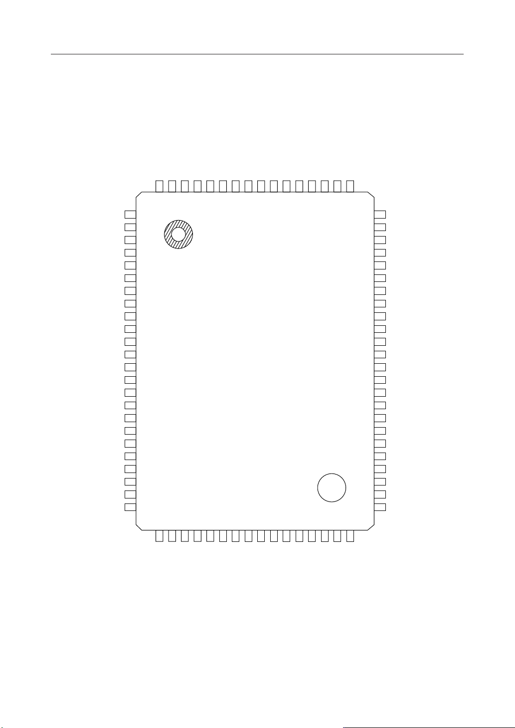
PIN CONFIGURATION (TOP VIEW)
ML9040-Axx/-Bxx GA
27
26
25
23
24
SEG
SEG
SEG
SEG
SEG
80
79
76
77
78
28
SEG
75
29
SEG
74
30
SEG
73
31
SEG
72
32
SEG
71
33
SEG
70
34
SEG
69
35
SEG
68
36
SEG
67
37
SEG
66
¡ SemiconductorML9040-Axx/-Bxx
38
SEG
65
SEG
SEG
SEG
SEG
SEG
SEG
SEG
SEG
SEG
SEG
SEG
SEG
SEG
SEG
SEG
SEG
SEG
SEG
SEG
SEG
SEG
SEG
GND
OSC
1
22
2
21
3
20
4
19
5
18
6
17
7
16
8
15
9
14
10
13
11
12
12
11
13
10
14
9
15
8
16
7
17
6
18
5
19
4
20
3
21
2
22
1
23
24
1
64
SEG
39
63
SEG
40
62
COM
16
61
COM
15
60
COM
14
59
COM
13
58
COM
12
57
COM
11
56
COM
10
55
COM
9
54
COM
COM
COM
COM
COM
COM
COM
COM
DB
DB
DB
DB
DB
DB
8
7
6
5
4
3
2
1
7
6
5
4
3
2
53
52
51
50
49
48
47
46
45
44
43
42
41
25
2
OSC
26
2
1
V
V
5
4
3
V
V
V
CP
DD
V
33
32L31
30
29
28
27
37RS36DO35DF34
R/W
40
39
38
1
0
E
DB
DB
80-Pin Plastic QFP
4

PIN DESCRIPTIONS
ML9040-Axx/-Bxx¡ Semiconductor
Symbol
Description
R/W Read/write selection input pin.
"H" : Read, and "L" : Write
RS Register selection input pin.
"H" : Data register, and "L" : Instruction register
E Input pin for data input/output with CPU and for instruction register activation.
DB0 - DB
OSC1, OSC
7
2
Input/output pins for data send/receive with CPU
Clock oscillating pins required for internal operation upon receipt of the LCD drive signal
and CPU instruction.
COM1 - COM
SEG1 - SEG
16
40
LCD COMMON signal output pins.
LCD SEGMENT signal output pins.
DO Output pin to be connected to MSM5259 to expand the number of characters to be
displayed.
CP Clock output pin used when DO pin data output shifts inside of MSM5259.
L Clock output pin for the serially transferred data to be latched to MSM5259.
DF The alternating current signal (Display Frequency) output pin.
V
DD
Power supply pin.
GND Ground pin.
V1, V2, V3, V4, V5Bias voltage input pins to drive the LCD.
5

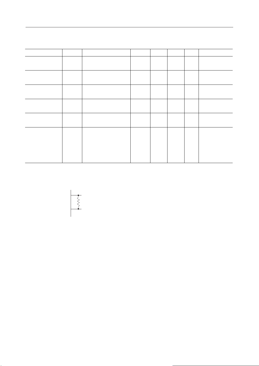
ABSOLUTE MAXIMUM RATINGS
¡ SemiconductorML9040-Axx/-Bxx
Parameter
Supply Voltage
LCD Driving Voltage
Input Voltage V
Power Dissipation P
Storage Temperature T
Symbol Condition Rating Unit Applicable pin
Ta = 25°C –0.3 to + 7.0 V VDD, GND
V
Ta = 25°C
DD
V
DD
Ta = 25°C –0.3 to V
— 500 mW —
— –55 to + 150 °C—
V
1
V
DD
, V2, V
V4, V
I
D
STG
3
5
RECOMMENDED OPERATING CONDITIONS
Parameter
Supply Voltage
Data Holding Voltage
LCD Driving Voltage
*1
*2
Operating Temperature T
*1 Voltage to assure Rf oscillation and register data retention.
*2 Voltage between VDD and V
*3 Voltages applicable to V1, V2, V3 and V4 are as follows.
V1 = VDD – 1/4 (VDD – V5)
V2 = V3 = VDD – 1/2 (VDD - V5)
V4 = VDD – 3/4 (VDD – V5)
*4 V1 = VDD – 1/5 (VDD – V5)
V2 = VDD – 2/5 (VDD – V5)
V3 = VDD – 3/5 (VDD – V5)
V4 = VDD – 4/5 (VDD – V5)
Symbol Condition Range Unit Applicable pin
V
V
DD
HOLD
V
LCD
5.
op
— 4.5 to 5.5 V VDD, GND
— 3.0 to 5.5 V VDD, GND
1/4 bias, VDD–V
1/5 bias, VDD–V
*3
3.0 to 6.0 V
5
*4
3.0 to 6.0 V
5
— –20 to + 75 °C—
– 8.0 to
+ 0.3
DD
+ 0.3 V
V
, V2, V
1
V
V4, V
3
5
R/W, RS, E,
DB
- DB
0
7
OSC
1
V
, V
DD
5
6

ELECTRICAL CHARACTERISTICS
DC Characteristics
Parameter
"H" Input Voltage
"L" Input Voltage V
"H" Input Voltage V
"L" Input Voltage V
"H" Output Voltage V
"L" Output Voltage V
"H" Output Voltage V
"L" Output Voltage V
Driver ON Resistor
(COM pins)
Driver ON Resistor
(SEG pins)
Input Leakage Current
Input Current I
Supply Current (1) I
Supply Current (2) I
LCD Driving Bias
Input Voltage
Schmitt voltage
width
Built-in reset
detection voltage
Symbol Condition Min. Typ. Max. Unit Applicable pin
— 2.2 — V
— –0.3 — 0.6 V
—V
— –0.3 — 1.0 V
IO = –0.205mA 2.4 — — V
IO = 1.2mA — — 0.4 V
IO = –40mA 0.9V
IO = 40mA — — 0.1V
VI = V
SS
= V
V
I
DD
R
V
R
IH1
IL1
IH2
IL2
OH1
OL1
OH2
OL2
COM
SEG
I
IL
IO = ±50mA, V
IO = ±50mA, V
VDD = 5.0V
= V
V
I
SS
VI = VDD, excluding current
IL2
flowing over pullup resistor
and output drive MOS
= 5.0V,
V
DD
resistor oscillation or
external clock input via
.
OSC
1
= 270kHz.
f
DD1
OSC
E is in "L" level.
Other inputs are open.
Output pins are
all no load. *1
VDD = 5.0V,
ceramic oscillation,
= 250kHz.
f
OSC
E is in "L" level.
DD2
Other pins are open.
Output pins are
all no load. *1
V
V
V
V
LCD1
V
LCD2
SUM
RES
DD–V5
——— TBD
——— — — 3.0 V V
*6
ML9040-Axx/-Bxx¡ Semiconductor
(V
= 4.5 to 5.5V, Ta = –20 to +75°C)
DD
DD
–1.0 — V
DD
— — V DO, CP, L,
DD
= 4V — — 20 kW COM1 - COM
LCD
= 4V — — 30 kW SEG1 - SEG
LCD
DD
——–1mA
——1mA
–50 –125 –250 mA
——2mA
— 0.35 0.6 mA
— 0.55 0.8 mA
1/5 bias — 6.0
1/4 bias — 6.0
3.0
3.0
TBD TBD V E
V R/W, RS, E,
V
V
DD
V
DB
DB
DC, OSC
R/W, RS
DB
VDD, V1, V2,
V
3
- DB
0
OSC
- DB
0
E
- DB
0
V
DD
V
DD
, V4, V
DD
7
1
7
2
16
40
7
5
7
¡ SemiconductorML9040-Axx/-Bxx
AC Characteristics
= 4.5 to 5.5V, Ta = –20 to +75°C)
(V
DD
Parameter
R
Clock Oscillation
f
Frequency
Clock Input
Frequency
Input Clock Duty f
Input Clock Rise
Time
Input Clock Fall
Time
Ceramic Unit
Oscillation
Frequency
Symbol Condition Min. Typ. Max. Unit Applicable pin
f
OSC1
f
DUTY
f
OSC
Rf = 91kW ± 2%
*2
OSC2 is open.
IN
Input from OSC
t
r
t
f
R
= 510kW,
f
= C2 = 200 pF,
C
1
= 30kW, and
R
d
1
175 250 350 kHz
125 250 350 kHz OSC
*3
*4
*4
45 50 55 % OSC
— — 0.2 ms OSC
— — 0.2 ms OSC
245 250 255 kHz
Ceralock CSB250A.
*5
*1 Applicable to the current that flows in pin VDD when power is input as follows:
VDD = 5V, GND = 0V, V1 = 3.4V, V2 = 1.8V, V3 = 0.2V, V4 = -1.4V, and V5 = -3V.
OSC
OSC
OSC
OSC
1
2
1
1
1
1
1
2
*2
OSC
OSC
1
R
f
2
Rf=91kW±2%
Minimum wiring is required between
OSC
and Rf and between OSC2 and Rf.
1
8
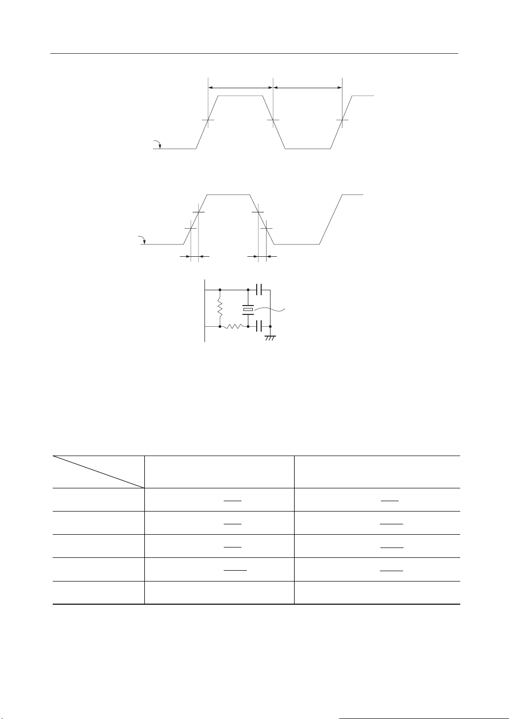
ML9040-Axx/-Bxx¡ Semiconductor
*3 Applied to pulse input via OSC
0.5V
f
IN
waveform
*4 Applied to pulse input via OSC
VDD–1.0V
fIN
waveform
*5
OSC
OSC
Ceralock : CSB250A (mfd. by MURATA MFG.Co.)
Please contact us when using this circuit.
.
1
DD
.(-Axx/-Bxx)
1
t
r
1
2
R
: 510kW ±5%
f
: 30kW ±5%
R
d
: 200pF ±10%
C
1
: 200pF ±10%
C
2
t
HW
0.5V
DD
f
= tHW/ (tHW + tLW) x 100(%)
DUTY
–1.0V
V
DD
1.0V1.0V
t
f
C
1
R
f
R
d
C
2
Ceralock
t
LW
0.5V
DD
*6 Input the voltage listed in the table below to V1 - V5:
N (LCD lines)
1-line mode 2-line mode
Pin
V
V
1
V
2
V
3
V
4
V
5
V
is an LCD driving voltage. (For "N" (number of LCD lines),
LCD
V
V
V
V
V
DD
DD
DD
DD
DD
–
–
–
–
– V
V
V
3V
LCD
LCD
4
LCD
2
LCD
2
LCD
4
refer to the initial set of the instruction code.)
V
LCD
–
V
DD
5
2V
LCD
–
V
DD
V
DD
V
DD
V
DD
–
–
– V
3V
4V
LCD
5
LCD
5
LCD
5
9
¡ SemiconductorML9040-Axx/-Bxx
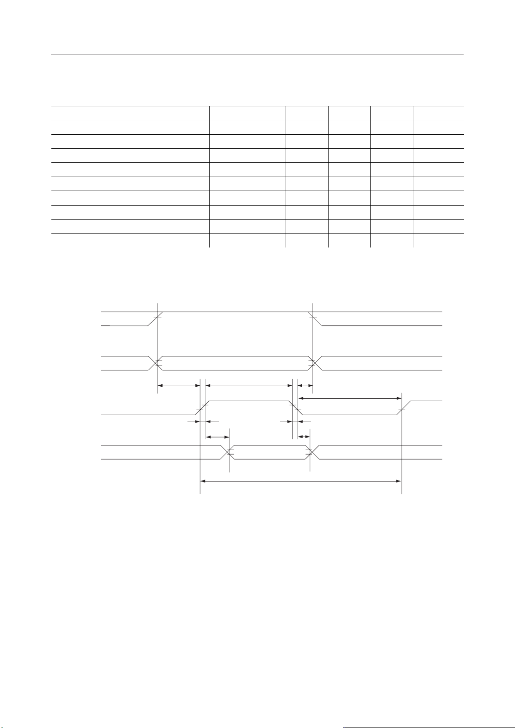
• Timing for output to the CPU
(V
= 4.5 to 4.5V, Ta = –20 to +75°C)
DD
Parameter
R/W and RS setup time
E "H" pulse width t
R/W and RS hold time t
E rise time t
E fall time t
E "L" pulse width t
E cycle time t
to DB7 data output delay time t
DB
0
to DB7 data output hold time t
DB
0
Symbol Min. Typ. Max. Unit
t
B
W
A
r
f
L
C
D
O
140 — — ns
280 — — ns
10 — — ns
— — 100 ns
— — 100 ns**
280 — — ns
667 — — ns
— — 220 ns
20 — — ns
* Values of tr and tf are design specification and are actually determined after sample
evaluation.
DB
0
R/W
-DB
RS
V
IH1
V
IH1
V
IL1
IH1
t
W
t
D
V
OH1
Output data
V
OL1
t
B
V
V
E
7
IL1
t
r
V
IH1
V
IH1
V
IL1
t
A
t
L
V
IH1
V
IL1
t
f
t
O
V
OH1
V
OL1
t
C
V
IL1
10
ML9040-Axx/-Bxx¡ Semiconductor
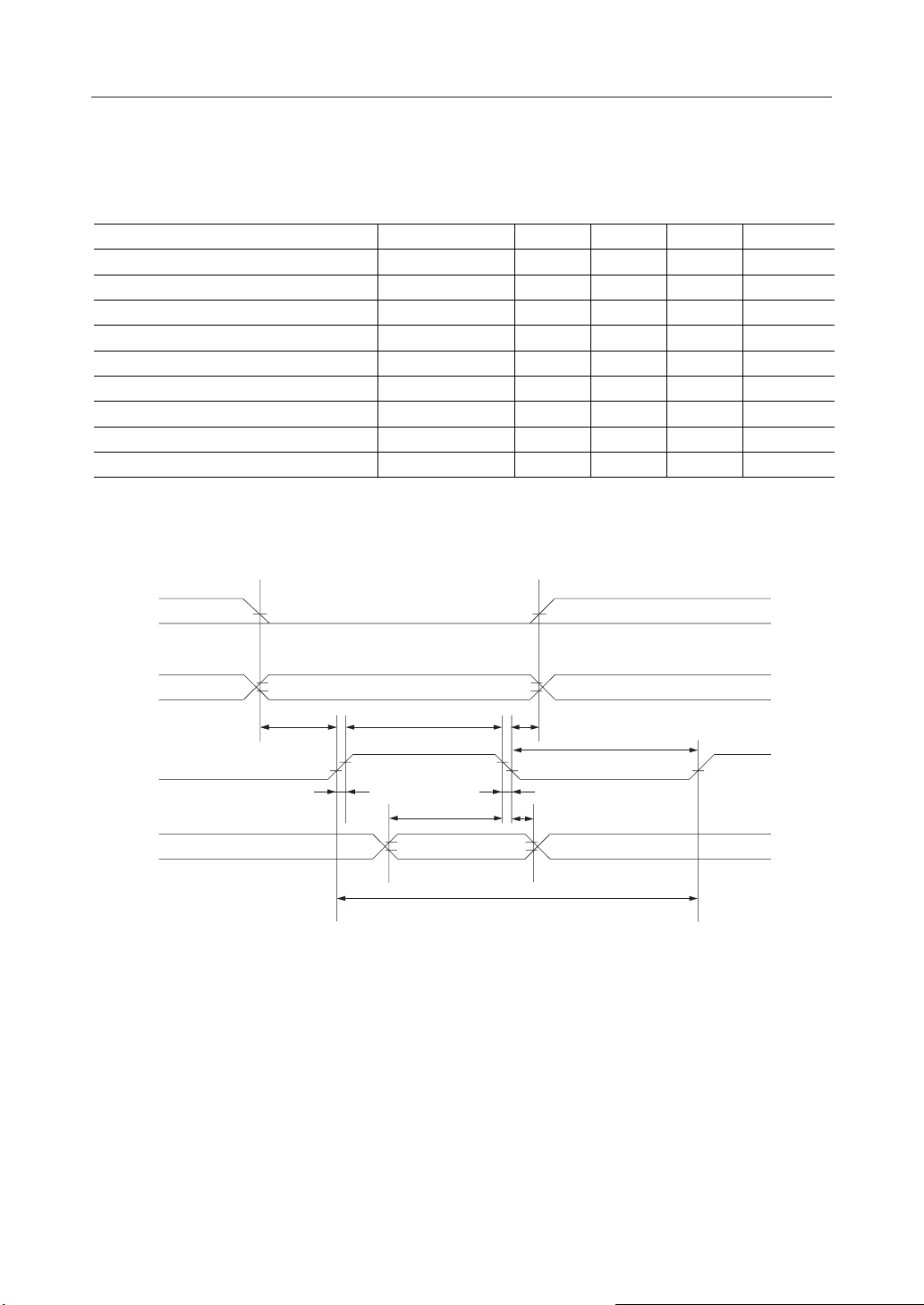
Switching Characteristics
• Timing for input from the CPU
(V
= 4.5 to 5.5V, Ta = –20 to +75°C)
DD
Parameter
R/W and RS setup time
E "H" pulse width t
R/W and RS hold time t
E rise time t
E fall time t
E "L" pulse width t
E cycle time t
to DB7 input data setup time t
DB
0
to DB7 input data hold time t
DB
0
* Values of tr and tf are design specification and are actually determined after sample
evaluation.
Symbol Min. Typ. Max. Unit
t
B
W
A
r
f
L
C
I
H
140 — — ns
280 — — ns
10—— ns
— — 100 ns
— — 100 ns**
280 — — ns
667 — — ns
180 — — ns
10—— ns
DB
0
- DB
R/W
RS
E
V
IL1
V
IH1
V
IL1
V
V
IH1
IL1
t
W
Input data
t
I
t
B
V
V
t
r
7
IH1
IL1
V
IL1
V
IH1
V
IL1
t
A
t
L
V
IH1
V
IL1
t
f
t
H
V
IH1
V
IL1
t
C
V
IL1
11

• Timing for output to MSM5259
Parameter
CP "H" pulse width
CP "L" pulse width t
DO setup time t
DO holding time t
"L" clock set-up time t
"L" clock hold time t
"L" "H" pulse width t
DF delay time t
¡ SemiconductorML9040-Axx/-Bxx
= 4.5 to 5.5V, Ta = –20 to +75°C)
(V
DD
Symbol Min. Typ. Max. Unit
t
HW1
HW2
LW
S
DH
SU
HO
M
800 — — ns
800 — — ns
300 — — ns
300 — — ns
500 — — ns
100 — — ns
800 — — ns
–1000 — 1000 ns
DO
CP
DF
V
OH2
V
OL2
t
t
HW1
V
OH2VOH2
t
LW
V
OL2
s
V
OH2
V
OL2
V
OH2
L
V
OH2
V
OL2
t
DH
V
V
OL2
t
t
SU
HW2
V
OH2
t
HO
V
OL2
t
M
V
OH2
OH2
12

ML9040-Axx/-Bxx¡ Semiconductor
FUNCTIONAL DESCRIPTION
Instruction Register (IR) and Data Register (DR)
These two registers are selected by the REGISTER SELECTION (RS) pin.
The DR is selected when the "H" level is input to the RS pin and IR is selected when the "L"
level is input.
The IR is used to store the address of the display data RAM (DD RAM) or character
generator RAM (CG RAM) and instruction code.
The IR can be written, but not be read by the microcomputer (CPU).
The DR is used to write and read the data to and from the DD RAM or CG RAM.
The data written to DR by the CPU is automatically written to the DD RAM or CG RAM
as an internal operation.
When an address code is written to IR, the data (of the specified address) is automatically
transferred from the DD RAM or CG RAM to the DR. Next, when the CPU reads the DR,
it is possible to verify DD RAM or CG RAM data from the DR data.
After the writing of DR by the CPU, the next adress in the DD RAM or CG RAM is selected
to be ready for the next CPU writing.
Likewise, after the reading out of DR by the CPU, DD RAM or CG RAM data is read out
by the DR to be ready for the next CPU reading.
Write/read to and from both registers is carried out by the READ/WRITE (R/W) pin.
Table 1 RS and R/W pins functions
R/W
L
H L Read of busy flag (BF) and address counter (ADC)
L H DR write
H H DR read
RS Function
L IR write
Busy Flag (BF)
When the busy flag is at "H", it indicates that the ML9040-Axx/-Bxx is engaged in internal
operation.
When the busy flag is at "H", any new instruction is ignored.
When R/W = "H" and RS = "L", the busy flag is output from DB7.
New instruction should be input when busy flag is "L" level.
When the busy flag is at "H", the output code of the address counter (ADC) is undefined.
Address Counter (ADC)
The address counter (ADC) allocates the address for the DD RAM and CG RAM write/
read and also for the cursor display.
When the instruction code for a DD RAM address or CG RAM address setting is input to
IR, after deciding whether it is DD RAM or CG RAM, the address code is transferred from
IR to ADC. After writing (reading) the display data to (from) the DD RAM or CG RAM,
the ADC is incremented (decremented) by 1 internally.
The data of the ADC is output to DB0 - DB6 on the conditions that R/W = "H", RS = "L", and
BF = "L".
13

¡ SemiconductorML9040-Axx/-Bxx
Timing Generator Circuit
This circuit is used to generate timing signals to activate internal operations upon receipt
of CPU instruction and also from such internal circuits as the DD RAM, CG RAM, and CG
ROM.
It is designed so that the internal operation caused by accessing from the CPU will not
interfer e with the internal operation caused by LCD driving. Consequently, when data
is written from the CPU to DD RAM, flickering does not occur in a display area other than
the display area where the data is written.
In addition, this circuit generates the transfer signal to MSM5259 for display character
expansion.
Display Data RAM (DD RAM)
This RAM is used to store display data of 8-bit character codes (see Table 2).
DD RAM address corresponds to the display position of the LCD. The correspondence
between the two is described in the following.
DD RAM address (set to ADC) is expressed in hexadecimal notation as shown below:
ADC
(Example)
When DD RAM
address is 2A
DB
6
Hexadecimal notation Hexadecimal notation
HLHLH
2A
DB
LSBMSB
0
LL
(1) Corresponden ce between address and display position in the 1-line display mode
First
digit
2023034045
01
00
MSB LSB
794F80
4E
Display position
DD RAM address (hex.)
(2) When the ML9040-Axx/-Bxx alone is used, up to 8 characters can be displayed from the
first to eighth digit.
First
digit
2023034045056067078
00
01
When the display is shifted by instruction, the correspondence between the LCD
display position and the DD RAM address changes as shown below:
First
digit
(Display
shifted
to right)
(Display
shifted
to left)
2013024035046057068
00
4F
First
digit
2033044055066077088
02
01
14
ML9040-Axx/-Bxx¡ Semiconductor
(3)When the ML9040-Axx/-Bxx is used with one MSM5259, up to 16 characters can be
displayed from the first to sixteenth digit as shown below:
First
digit
2023034045056067078
00
01
100A110B120C130D140E150F169
08 09
MSM5259 displayML9040-Axx/-Bxx display
When the display is shifted by instruction, the correspondence between the LCD
display and the DD RAM address changes as shown below:
First
digit
(Display shifted to right)
2013024035046057068
4F
00
01
02 03 04 05 06 07 08 09 0A 0B 0C 0D 0E 0F 10(Display shifted to left)
07
1009110A120B130C140D150E169
08
MSM5259 displayML9040-Axx/-Bxx display
(4)Since the ML9040-Axx/-Bxx has a DD RAM capacity of up to 80 characters, up to 9
MSM5259 devices can be connected to ML9040-Axx/-Bxx so that 80 characters can be
displayed.
First
digit
2023034045056067078
01
00
08
100A110B120C130D140E150F169
09
1817
10 11
MSM5259 (1) displayML9040-Axx/-Bxx display
- (8) display
744A754B764C774D784E794F8073
48 49
MSM5259 (9) displayMSM5259 (2)
15
 Loading...