


OKI Semiconductor
PEDL87V21071-01
Issue Date: Nov. 15, 2005
ML87V21071
Video Signal Noise Reduction IC with a Built-in Frame Memory
Preliminary
GENERAL DESCRIPTION
The ML87V21071, which comprises a frame memory and signal processing and memory control logic circuits, has
achieved motion-adaptive 3D noise reduction.
To perform noise reduction with afterimage suppression, the ML87V210 71 also enables noise reduction using the
edge-adaptive 2D noise reduction filter.
Each noise reduction function allows setting an automatic mode. In automatic mode, noise of a vertical blanking
period and a valid data peri od is detected t o reduce noi se accordin g to the noise status fro m which t he noise reduct ion
setting value is detected.
The ML87V21071 also has a cross-color cancellation function that uses the motion-adaptive 3D comb filter method
that removes cross colors occurring at two-dimensional YC separation in the NTSC/PAL system.
Since the same format as the input can be selected for outpu t, n oise re ducti on can ea sil y be achie ved by i nsertin g t he
IC into the conventional system.
FEATURES
• Built-in memory:
Frame memory (78 × 608 × 16-bit) × 1 unit
• Maximum input and output operating frequencies (16-bit/8-bit, ITU-R BT.656):
14.75/29.5 MHz
* For 525p/625p, only 16-bit input mode is supported (Max.: 29.5 MHz).
• Power supply voltage:
3.3 V ± 0.3 V
• Input/ouput pin:
LVCMOS (3.3 V)
• Input/ouput data format:
YCbCr (8 bit (Y) + 8 bit (CbCr))(4:2:2): 16-bit mode
YCbCr (8 bit (YCbCr))(4:2:2): 8-bit mode
ITU-R656 (8 bit (YCbCr)): ITU-R BT.656 mode
* In 16-bit input mode, neither 8-bit mode nor ITU-R BT.656 mode can be selected for output.
• Serial bus:
2
C-bus interface: (400 kHz, 100 kHz)
I
• Memory controller:
Compatible with 625/50Hz 2:1(625i), 525/60Hz 2:1(525i), 625/50Hz 1:1(625p), and 525/60Hz 1:1(525p)
• Motion-adaptive 3D noise reduction:
Frame-field-line-correlation noise detection and noise subtraction method
Supports automatic noise reduction setting
• Edge-adaptive 2D noise reduction:
Edge-adaptive space filter used
• Chrominance signal cross color cancelling:
Motion-adaptive 3D comb filter used
Compatible with 525i (NTSC decode signal)/625i (PAL decode signal)
• Package:
100-pin TQFP (TQFP100-P-1414-0.50-K) (ML87V21071TB)
1/123
PEDL87V21071-01
OKI Semiconductor
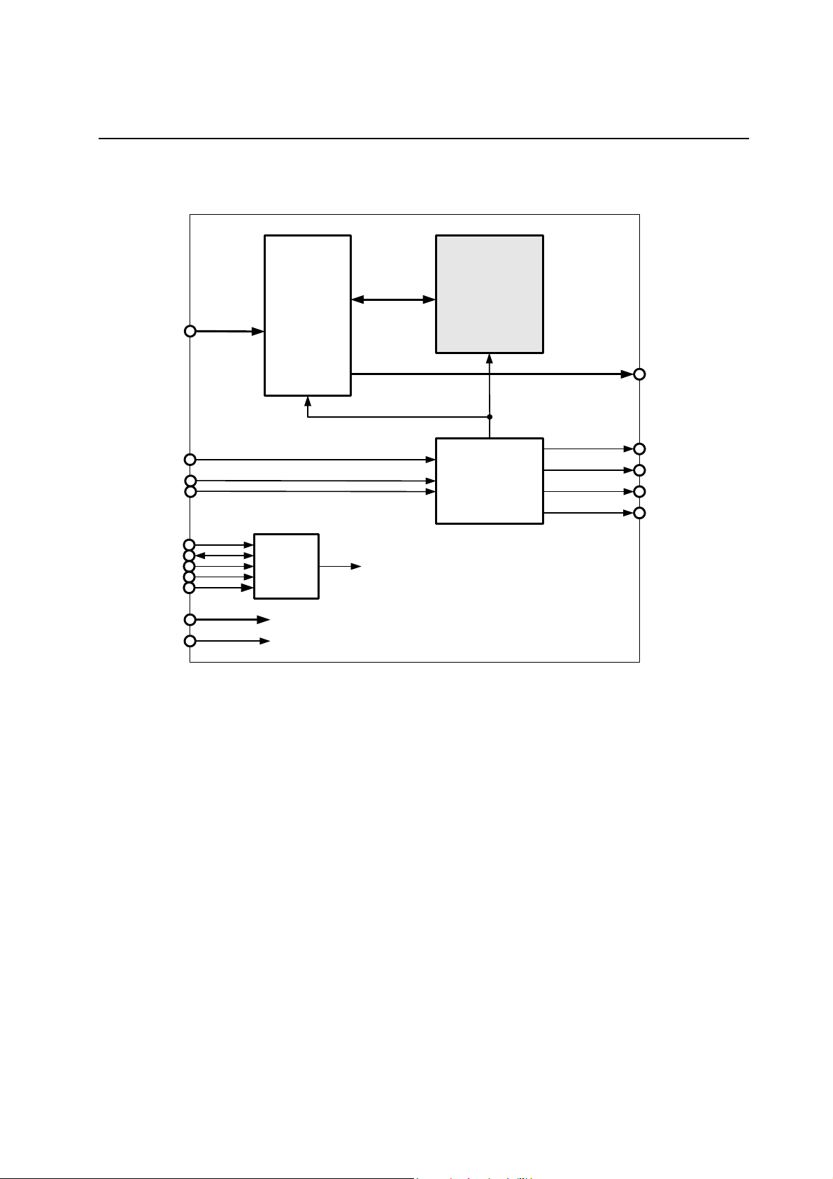
BLOCK DIAGRAM
YI0-7
CI0-7
ICLK
IVS
IHS
x16
Input/Output
Process
Block
+
3D NR
+
2D NR
+
CC
x16
Frame
Memory
Memory
Controller
x16
ML87V21071
YO0-7
CO0-7
OVS
OHS
HREF
CLKO
SCL
SDA
SLA1
SLA2
MODE0-4
TEST0-5
RESET
I2C-bus
I/F
Register
Control
Signal
2/123

PEDL87V21071-01
OKI Semiconductor
PIN CONFIGURATION (TOP VIEW)
VDD
N.C.
V
MODE3
MODE4
N.C.
OE
N.C.
N.C.
N.C.
N.C.
TEST5
VDD
TEST4
TEST3
TEST2
TEST1
TEST0
N.C.
N.C.
TESTM
TSELF
VSS
N.C.
V
SS
TEST6
RESET
74
75
76
77
78
SS
79
80
81
82
83
84
85
86
87
88
89
90
91
92
93
94
95
96
97
98
99
100
DD
YO7
TEST7
V
71
72
73
YO4
YO6
YO5
68
69
70
VDD
YO3
YO2
65
66
67
SS
N.C.
V
YO1
YO0
63
64
VDD
60
61
62
ML87V21071TB
(TQFP100-P-1414-0.5-K)
CO7
59
CO6
58
CO5
57
CO4
56
ML87V21071
VSS
CO3
CO2
CO1
CO0
51
52
53
54
55
50
VDD
49
N.C.
48
SS
V
47
HREF
46
OVS
45
OHS
44
N.C.
43
N.C.
42
N.C.
41
N.C.
40
V
DD
39
N.C.
38
N.C.
37
VSS
36
VDD
35
CLKO
34
MODE2
33
N.C.
32
MODE1
31
MODE0
30
IHS
29
IVS
28
VSS
27
N.C.
26
V
DD
1
YI7
YI6
VSS
N.C.
SCL
SDA
SLA1
SLA2
YI5
12
11
10
YI3
YI2
YI4
15
14
13
DD
YI1
YI0
V
16
ICLK
18
17
CI7
VSS
21
20
19
CI6
CI5
CI4
24
23
22
CI3
25
CI2
CI1
CI0
9
8
7
6
5
4
3
2
3/123

PEDL87V21071-01
OKI Semiconductor
PIN DESCRIPTIONS
No. Symbol I/O Pad Remarks Pin Description
1 N.C. —
2 VSS —
3 SDA I/O
4 SCL I Schmitt
5 SLA1 I
6 SLA2 I
7 YI7 I
8 YI6 I
9 YI5 I
10 YI4 I
11 YI3 I
12 YI2 I
13 YI1 I
14 YI0 I
15 VDD —
16 ICLK I
17 VSS —
18 CI7 I pull-down 50k
19 CI6 I pull-down 50k
20 CI5 I pull-down 50k
21 CI4 I pull-down 50k
22 CI3 I pull-down 50k
23 CI2 I pull-down 50k
24 CI1 I pull-down 50k
25 CI0 I pull-down 50k
26 VDD —
27 N.C. —
28 VSS —
29 IVS I
30 IHS I
31 MODE0 I
32 MODE1 I
33 N.C. —
Schmitt(IN)/
OpenDrain(OUT)
Schmitt
pull-down 50k
Schmitt
pull-down 50k
Schmitt
pull-down 50k
Schmitt
pull-down 50k
Schmitt
pull-down 50k
Schmitt
pull-down 50k
Unused pin
Ground
2
I
C-bus data pin
2
C-bus clock pin
I
Slave address setting pin bit 1
Slave address setting pin bit 2
Luminance signal input pin bit 7 (MSB)
Luminance signal input pin bit 6
Luminance signal input pin bit 5
Luminance signal input pin bit 4
Luminance signal input pin bit 3
Luminance signal input pin bit 2
Luminance signal input pin bit 1
Luminance signal input pin bit 0 (LSB)
3.3 V power supply
System clock Input pin
Ground
Chrominance signal input pin bit 7 (MSB)
Chrominance signal input pin bit 6
Chrominance signal input pin bit 5
Chrominance signal input pin bit 4
Chrominance signal input pin bit 3
Chrominance signal input pin bit 2
Chrominance signal input pin bit 1
Chrominance signal input pin bit 0 (LSB)
3.3 V power supply
Unused pin
Ground
Input system vertical Sync. signal input pin
Input system horizontal Sync. signal input pin
Mode setting pin bit 0
(Equivalent to internal register VMD[0])
Mode setting pin bit 1
(Equivalent to internal register HMD[0])
Unused pin
ML87V21071
Termination of
unused pin
Not used
X
X
X
Not used or
connected to GND
Not used or
connected to GND
X
X
X
X
X
X
X
X
X
X
X
Not used or
connected to GND
Not used or
connected to GND
Not used or
connected to GND
Not used or
connected to GND
Not used or
connected to GND
Not used or
connected to GND
Not used or
connected to GND
Not used or
connected to GND
X
Not used
X
Not used or
connected to GND
Not used or
connected to GND
Not used or
connected to GND
Not used or
connected to GND
Not used
4/123

PEDL87V21071-01
OKI Semiconductor
No. Symbol I/O Pad Remarks Pin Description
34 MODE2 I
35 CLKO O
36 VDD —
37 VSS —
38 N.C. —
39 N.C. —
40 VDD —
41 N.C. —
42 N.C. —
43 N.C. —
44 N.C. —
45 OHS O
46 OVS O
47 HREF O
48 VSS —
49 N.C. —
50 VDD —
51 CO0 O
52 CO1 O
53 CO2 O
54 CO3 O
55 VSS —
56 CO4 O
57 CO5 O
58 CO6 O
59 CO7 O
60 VDD —
61 N.C. —
62 VSS —
63 YO0 O
64 YO1 O
65 YO2 O
66 YO3 O
67 VDD —
68 YO4 O
69 YO5 O
70 YO6 O
71 YO7 O
72 VSS —
73 TEST7 I
74 TEST6 I
75
76 VDD —
RESET
I Schmitt
Schmitt
pull-down 50k
Schmitt
pull-down 50k
Schmitt
pull-down 50k
Mode setting pin bit 2
(Equivalent to internal register DISEL[0])
Clock output (I
3.3 V power supply
Ground
Unused pin
Unused pin
3.3 V power supply
Unused pin
Unused pin
Unused pin
Unused pin
Horizontal Sync. signal output pin
Vertical Sync. signal output pin
Data output horizontal reference signal output
pin
Ground
Unused pin
3.3 V power supply
Chrominance signal output pin bit 0 (LSB)
Chrominance signal output pin bit 1
Chrominance signal output pin bit 2
Chrominance signal output pin bit 3
Ground
Chrominance signal output pin bit 4
Chrominance signal output pin bit 5
Chrominance signal output pin bit 6
Chrominance signal output pin bit 7 (MSB)
3.3 V power supply
Unused pin
Ground
Luminance signal output pin bit 0 (LSB)
Luminance signal output pin bit 1
Luminance signal output pin bit 2
Luminance signal output pin bit 3
3.3 V power supply
Luminance signal output pin bit 4
Luminance signal output pin bit 5
Luminance signal output pin bit 6
Luminance signal output pin bit 7 (MSB)
Ground
Test input pin bit 7 (1: Test mode)
Test input pin bit 6 (1: Test mode)
System reset/input pin
0: System reset
1: Operation
3.3 V power supply
2
C-bus control possible)
ML87V21071
Termination of
unused pin
Not used or
connected to GND
Not used
X
X
Not used
Not used
X
Not used
Not used
Not used
Not used
Not used
Not used
Not used
X
Not used
X
Not used
Not used
Not used
Not used
X
Not used
Not used
Not used
Not used
X
Not used
X
X
X
X
X
X
X
X
X
X
X
Not used or
connected to GND
Not used or
connected to GND
X
X
5/123

PEDL87V21071-01
OKI Semiconductor
No. Symbol I/O Pad Remarks Pin Description
77 N.C. —
78 VSS —
79 MODE3 I
80 MODE4 I
81 N.C. —
82 OE —
83 N.C. —
84 N.C. —
85 N.C. —
86 N.C. —
87 TEST5 I
88 VDD —
89 TEST4 I
90 TEST3 I
91 TEST2 I
92 TEST1 I
93 TEST0 I
94 N.C. —
95 N.C. —
96 TESTM I
97 SELF I
98 VSS —
99 N.C. —
100 VDD —
Schmitt
pull-down 50k
Schmitt
pull-down 50k
Schmitt
pull-down 50k
Schmitt
pull-down 50k
Schmitt
pull-down 50k
Schmitt
pull-down 50k
Schmitt
pull-down 50k
Schmitt
pull-down 50k
Schmitt
pull-down 50k
Schmitt
pull-down 50k
Schmitt
pull-down 50k
Unused pin
Ground
Mode setting pin bit 3
(Equivalent to internal register R656I)
Mode setting pin bit 4
(Equivalent to internal register DOSEL)
Unused pin
Output enable input pin
Unused pin
Unused pin
Unused pin
Unused pin
Test input pin bit 5 (1: test mode)
3.3 V power supply
Test input pin bit 4 (1: test mode)
Test input pin bit 3 (1: test mode)
Test input pin bit 2 (1: test mode)
Test input pin bit 1 (1: test mode)
Test input pin bit 0 (1: test mode)
Unused pin
Unused pin
Memory test input pin (1: test mode)
Self refresh test input setting pin
Ground
Unused pin
3.3 V power supply
ML87V21071
Termination of
unused pin
Not used
X
Not used or
connected to GND
Not used or
connected to GND
Not used
Not used or
connected to GND
Not used
Not used
Not used
Not used
Not used or
connected to GND
X
Not used or
connected to GND
Not used or
connected to GND
Not used or
connected to GND
Not used or
connected to GND
Not used or
connected to GND
Not used
Not used
Not used or
connected to GND
Not used or
connected to GND
X
Not used
X
6/123
PEDL87V21071-01
OKI Semiconductor
ML87V21071
ELECTRICAL CHARACTERISTICS
Absolute Maximum Ratings
Parameter Symbol Condition Rating Unit
Power supply voltage
Input pin voltage
Output pin short-circuit current
Power dissipation
Operating temperature
Storage temperature
Recommended Operating Conditions
Parameter Symbol Min. Typ. Max. Unit
Power supply voltage VDD 3.0 3.3 3.6 V
Power supply voltage VSS 0 0 0 V
Operating temperature
Pin Capacitance
Parameter Symbol Min. Max. Unit
Input capacitance Ci — 7 pF
Input/output capacitance (SDA) Cio — 7 pF
Output capacitance Co — 7 pF
V
DD
V
I
I
OS
P
D
T
— 0 to 70
opr
T
— –50 to +150
stg
Ta = 25°C
Ta = 25°C –0.5 to V
Ta = 25°C
Ta = 25°C
–0.5 to +4.6 V
+ 0.5 ≤ 4.6
DD
50 mA
1 W
Ta 0 — 70
(VCC = 3.3 V ± 0.3 V, f = 1 MHz, Ta = 25°C)
V
°C
°C
°C
7/123

PEDL87V21071-01
OKI Semiconductor
ML87V21071
DC Characteristics
(Ta = 0 to 70°C)
Parameter Symbol Condition Min. Max. Unit
V
“H” level input voltage V
“L” level input voltage V
“H” level input voltage
(TEST1–TEST7, TESTM, SELF)
“L” level input voltage
(TEST1–TEST7, TESTM, SELF)
“H” level input voltage
(SDA, SCL, IVS, IHS, RESET)
“L” level input voltage
(SDA, SCL, IVS, IHS, RESET)
—
IH1
—
IL1
V
IH2
V
IL2
V
Schmitt
IH3
Schmitt –0.3
V
IL3
—
—
V
V
V
DD
–0.3
DD
–0.3
DD
× 0.7
× 0.75
× 0.75
+0.3 V
DD
× 0.3
V
DD
+0.3 V
V
DD
V
× 0.25
DD
+0.3 V
V
DD
V
× 0.25
DD
V
V
V
“H” level input current (pull-down) IIH 50 kΩ pull down 20 200 µA
Input leakage current IIL — –10 +10 µA
“H” level output voltage (other than SDA) VOH I
“L” level output voltage (other than SDA) VOL I
“L” level output voltage (N-Ch. OD)
(SDA)
V
I
OOL
Output leakage current IOL
Supply current (during operation) I
Supply current (during standby) I
DD1
Input pin = 0 V — 5 mA
DD2
= –4 mA 2.4 VDD V
OH
= 4 mA 0 0.4 V
OL
= 4 mA 0 0.4 V
OL
0 ≤ V
≤ VDD
out
Output disabled
ICLK: 29.5MHz
Output disabled
–10 +10 µA
— 100 (TBD) mA
AC Characteristics
(Ta = 0 to 70°C)
Parameter Symbol Condition Min. Max. Unit
t
ICLK clock cycle time
ICLK clock duty ratio
ICLK input set-up time
ICLK input hold time
ICLK output delay time
CLKO delay time
Data through time
— 33 — ns
ICLK
dt
— 40 60 %
ICLK
t
— 5 — ns
IISU
t
— 3 — ns
IIH
t
C
IOD
t
CKD
t
DIDO
CL = 30 pF (IICLK output) 2 25
C
L
C
= 30pF 2 25 ns
L
= 30 pF (ICLK output) 2 17
= 30 pF 2 17 ns
L
ns
Note 1: Measurement conditions
Output comparison level: V
Input voltage level: V
IH
= VDD/2, VOL = VDD/2
OH
= VDD, VIL = 0.0 V
Note 2: Input/output data for the internal memory is guaranteed from the third input-system vertical synchronization
signal with RESET = 1 after V
reaches 3.0 V after the power is turned on. (Due to memory initialization,
DD
the first and second data for two fields is not guaranteed.)
8/123
PEDL87V21071-01
OKI Semiconductor
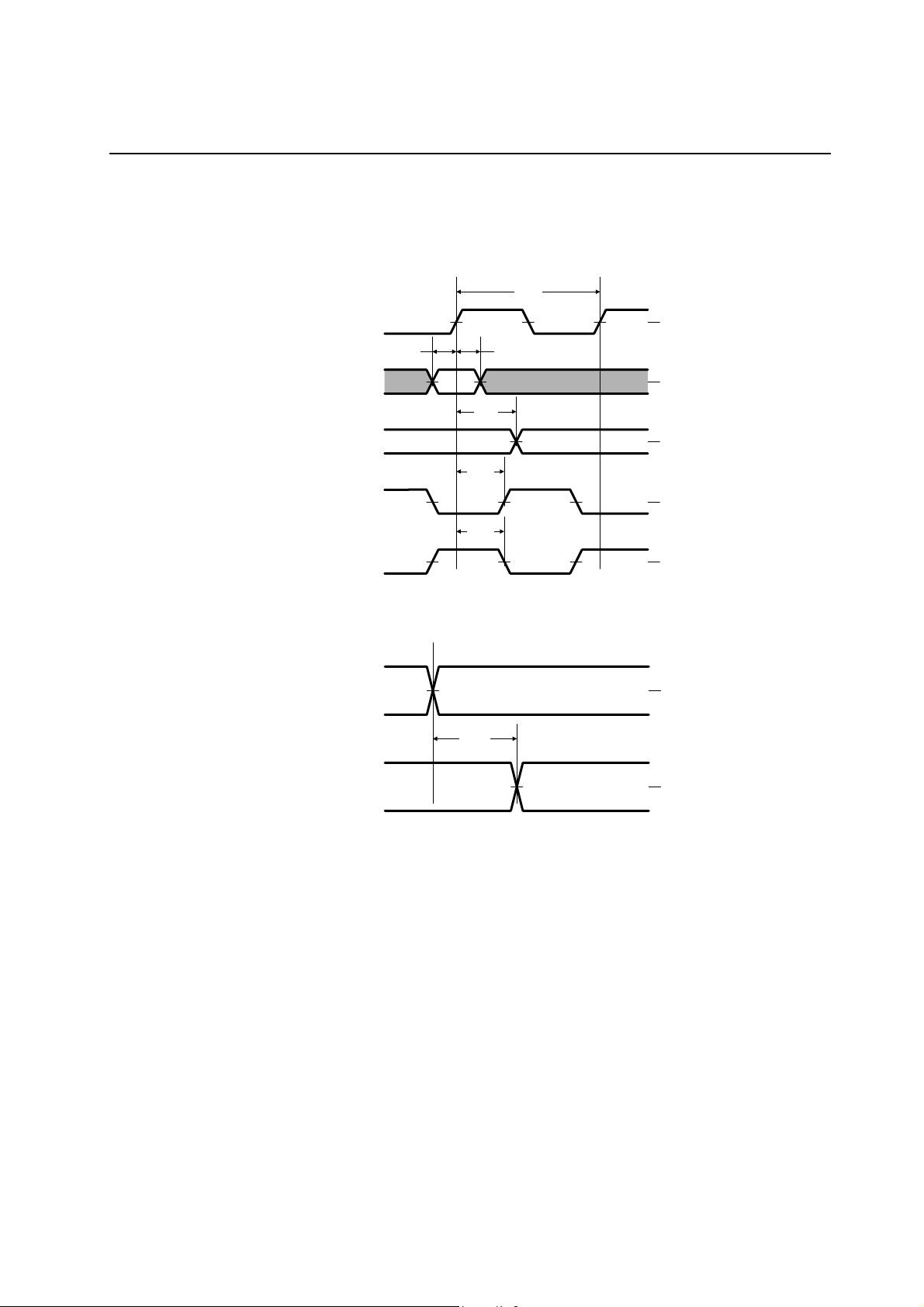
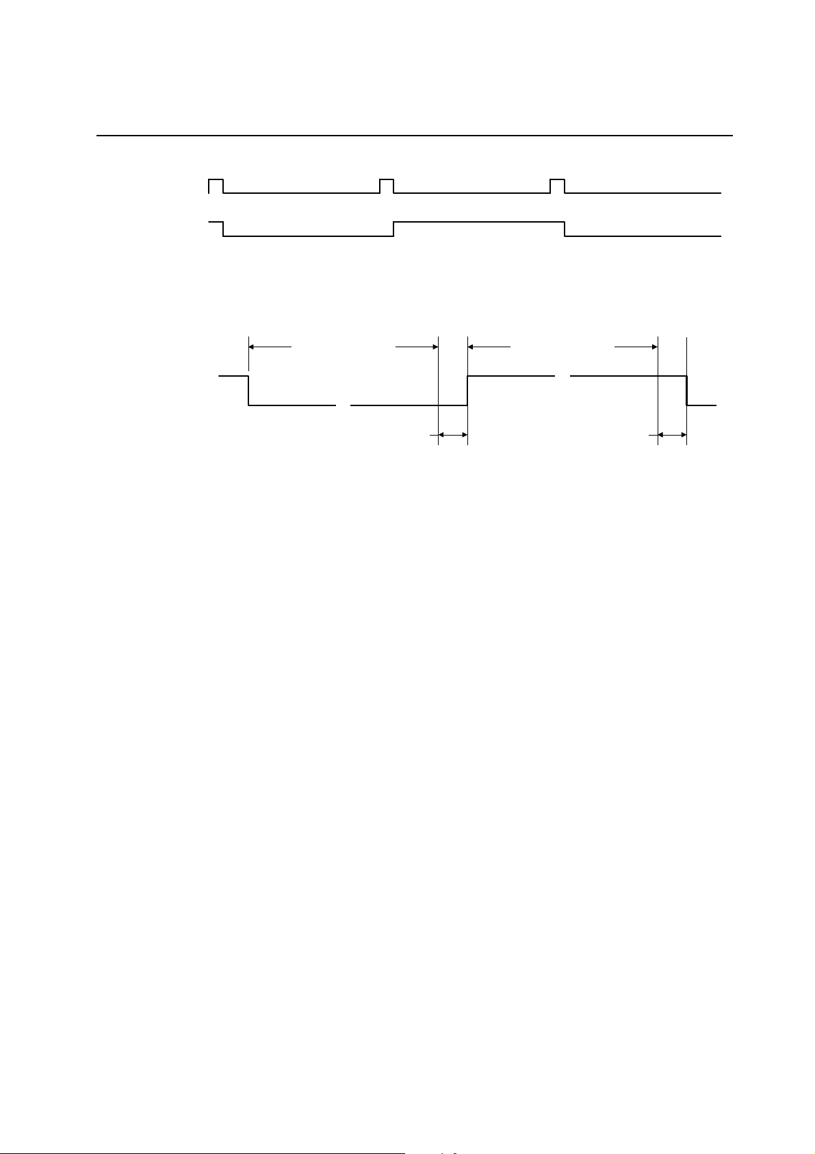
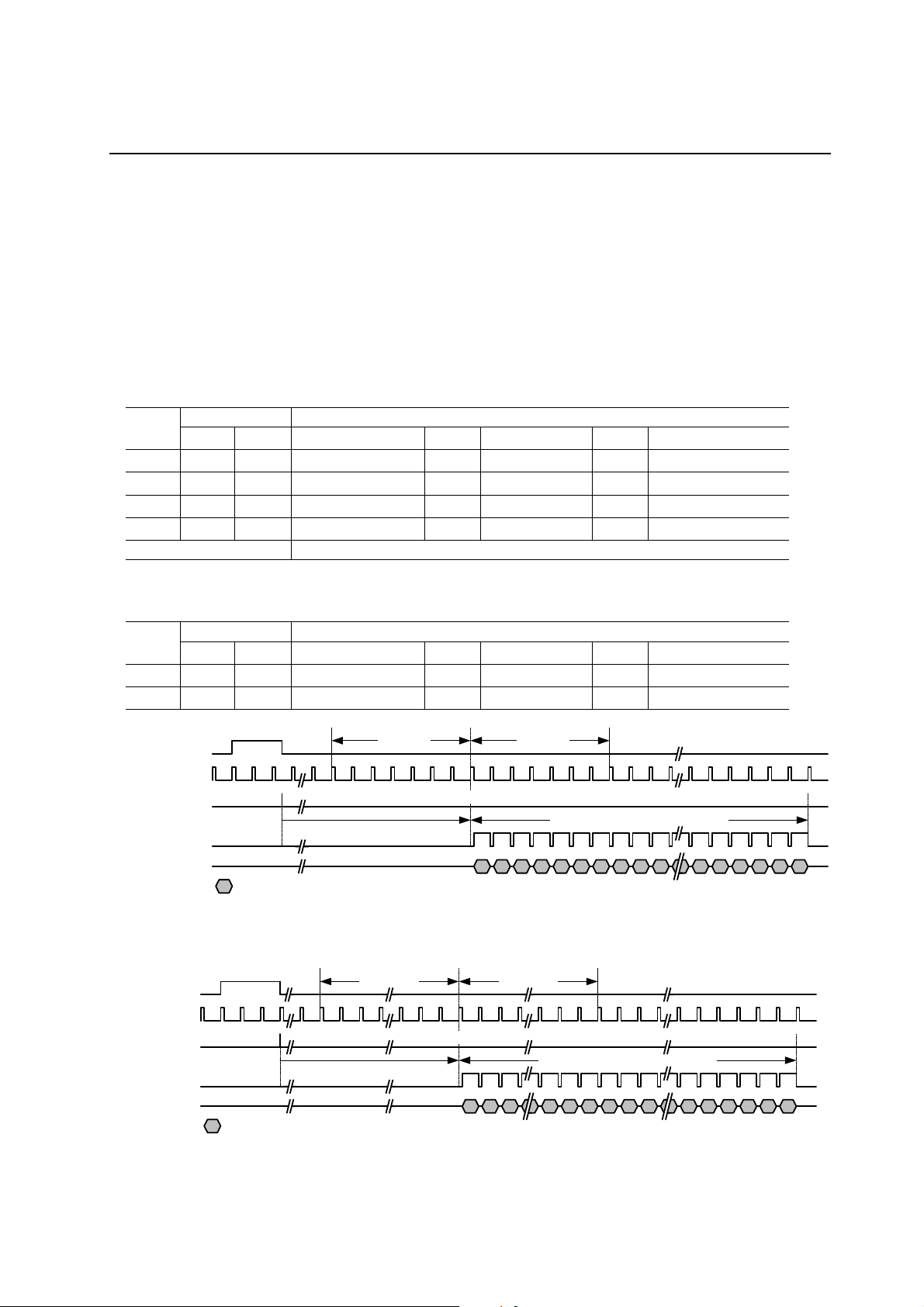
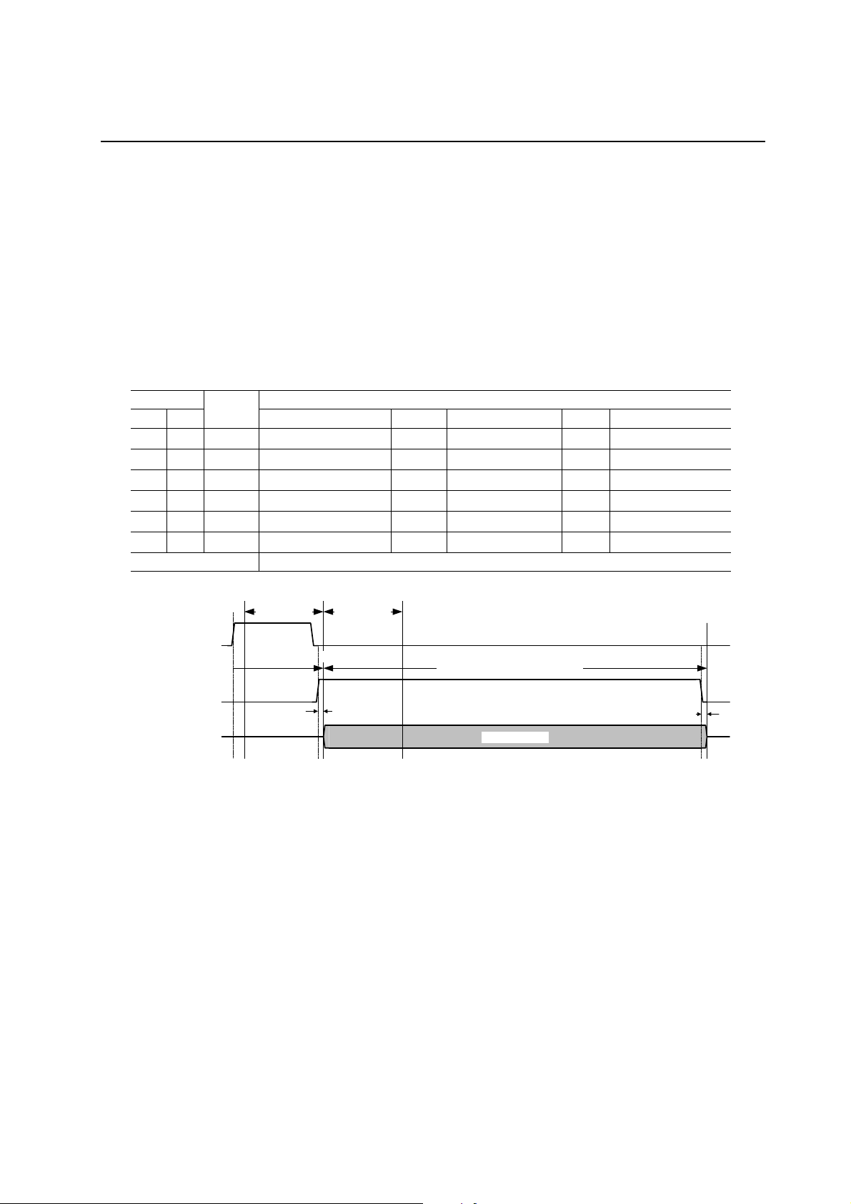
INPUT/OUTPUT TIMING
1. ICLK Input/Output Timing
ICLK
DATA &
CONTROL
INPUT (ICLK)
DATA &
CONTROL
OUTPUT (ICLK)
CLKO
(CKINV=0)
CLKO
(CKINV=1)
2. Data through Mode Input/Output Timing
t
IISU
t
CKD
t
CKD
t
IOD
ML87V21071
t
ICLK
50%
t
IIH
50%
50%
50%
50%
DATA &
CONTROL
INPUT
DATA &
CONTROL
OUTPUT
t
DIDO
50%
50%
9/123
PEDL87V21071-01
OKI Semiconductor
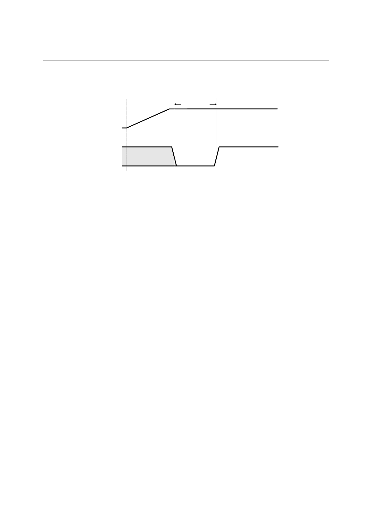
3. System Reset Timing
Power ON
1ms (Min.)
Power
supply
voltage
RESET
* When the power supply voltage reaches V
RESET pin for 1 ms or more to initialize the internal circuits.
* After the RESET pin goes to 1, the I
Don't care
(3.0 to 3.6 V) from 0 V after power is turned on, input 0 to the
DD
2
C-bus interface can be used while the input of ICLK is stable.
ML87V21071
V
DD
0 V
V
DD
0 V
10/123
PEDL87V21071-01
OKI Semiconductor
ML87V21071
FUNCTIONAL DESCRIPTION
1. Input/Output
1.1 Memory Control
The ML87V21071 accesses data to the input data frame memory by generating a line access type memory control
signal from Sync. signals of the IVS and IHS pin inputs or the Sync. signals separated from SAV and EAV, and
achieves noise reduction of frame/field/line adaptation recursive type.
1.1.1 Input Control Mode Settings
As shown in the table below, this IC offer s a choi ce of 12 i nput cont rol m odes includi ng the progressi ve m ode by
the INPR setting (SUB:44h-bit[7]), which can be selected by setting either the external setting pin mode (IRMON
= 0 (SUB: 40h–bit [7]) or internal register mode (IRMON = 1).
In ITU-R BT.656 input mode and i n the m ode of vali d 720 pixel s in the horizont al directi on (HM D[1:0] =0h), the
IC checks the mode by measuring the blanking period (between EAV and SAV) of the timing reference code of
the input data (YI[7:0]) and automatically sets VMD[0] by setting APN656 = 1 (SUB: 41h-bit[2]).
During APN656=1, do not set any value other than HMD[1:0]=1.
Table F1-1-1 (1) Input Control Mode Setting Allocation 1
IRMON
0 SUB:40h-bit[1]
1 SUB:40h-bit[1] SUB:40h-bit[0] SUB:40h-bit[3] SUB:40h-bit[2]
[1] [0] [1] [0]
VMD HMD
MODE 0
(External pin)
SUB:40h-bit[3]
MODE 1
(External pin)
Table F1-1-1 (2) Input Control Mode Setting Allocation 2
INPR Mode
0 Interlace (525i/625i)
1 Progressive (525p/625p)
* In progressive mode, neithe r 8-bit input m ode nor ITU-R BT.6 56 input mode can be
seected.
Table F1-1-1 (3) Input Control Mode Settings(INPR=0: Interlace)
VMD HMD
[1] [0] [1] [0]
0 0 0 0 625/50Hz 2:1 288 13.5/27 864 720
0 1 0 0 525/60Hz 2:1 243 13.5/27 858 720
0 0 0 1 625/50Hz 2:1 288 14.75/29.5 944 768
0 1 0 1 525/60Hz 2:1 243
0 0 1 0 625/50Hz 2:1 288 14.75/29.5 944 768
0 1 1 0 525/60Hz 2:1 243
Other than above Test modes
Vertical mode
The input system internal clock frequency f
16-bit input mode: f
IICLK
= f
ICLK
8-bit input mode/ITU-R BT.656 mode: f
Number of
valid lines
is as follows:
IICLK
= f
IICLK
Standard clock
frequency f
12.272727/
24.545454
14.31818/
28.63636
/2
ICLK
[MHz]
ICLK
Standard pixels
per line
780 640
910 768
Valid pixels
11/123

PEDL87V21071-01
OKI Semiconductor
ML87V21071
Table F1-1-1 (4) Input Control Mode Settings(INPR=1: Progressive)
VMD HMD
[1] [0] [1] [0]
Vertical mode
Number of
valid lines
0 0 0 0 625/50Hz 1:1 288 27 864 720
0 1 0 0 525/60Hz 1:1 243 27 858 720
0 0 0 1 625/50Hz 1:1 288 29.5 944 768
0 1 0 1 525/60Hz 1:1 243 24.545454 780 640
0 0 1 0 625/50Hz 1:1 288 29.5 944 768
0 1 1 0 525/60Hz 1:1 243 28.63636 910 768
Other than above Test modes
The input system internal clock frequency f
16-bit input mode: f
IICLK
= f
ICLK
is as follows:
IICLK
Standard clock
frequency f
ICLK
[MHz]
Standard pixels
per line
Valid pixels
12/123

PEDL87V21071-01
OKI Semiconductor
ML87V21071
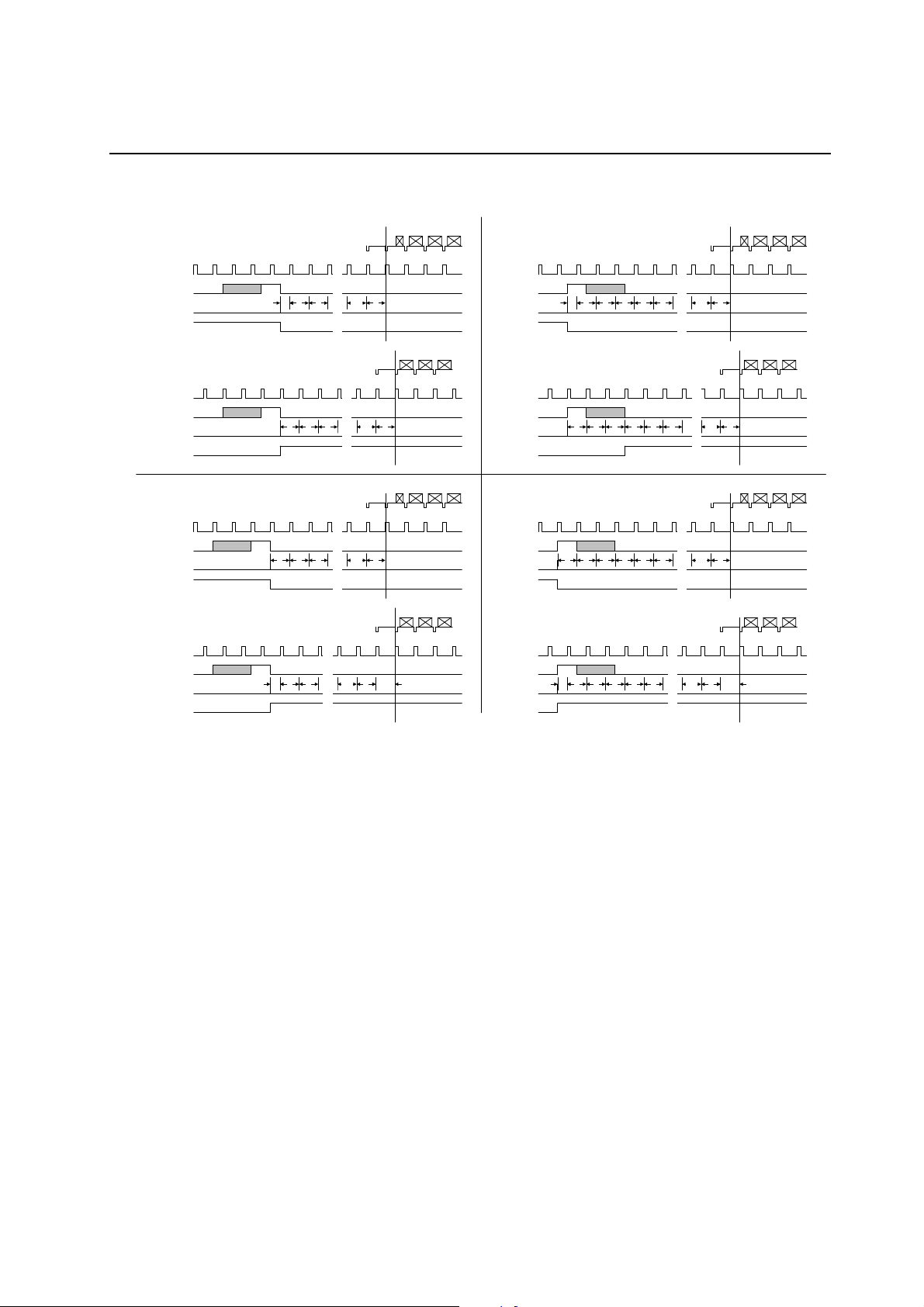
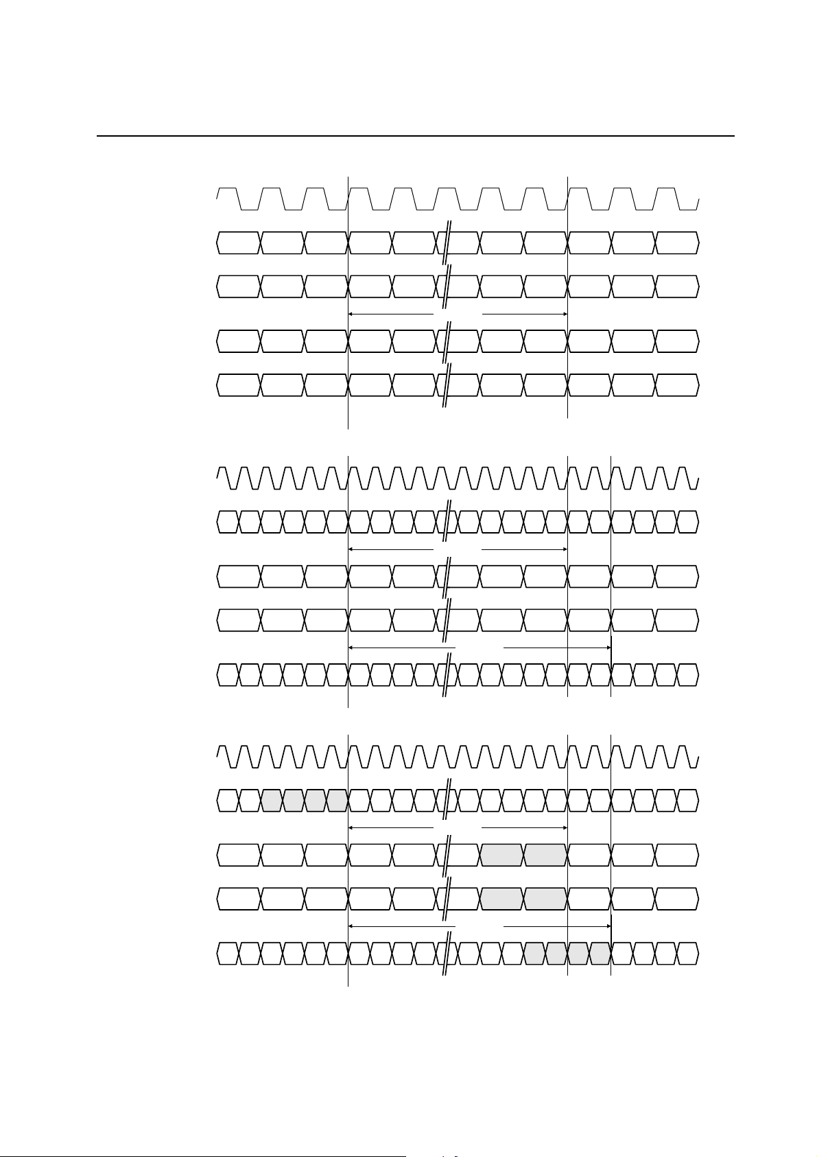
1.1.2 Input System Field Detection
The IC detects the input data field from the phase of IVS and IHS and generates the input field pulse (IF) to
control the internal memory.
The field detection pulse can be selected from the IHS (IFLS = 0) or from 0.5H pulse IHALF (IFLS = 1) by setting
2
the I
C-bus setting register IFLS (SUB:42h-bit[3]).
In the rear edge of judgment area, since the field ju dgm ent uncert ainty are a cont ains 10 c locks o f IICL K (inter nal
input system clock), external phase adjustment will be necessary if the phase of IVS lies in this area. (However,
there is no problem if the change of IVS and IHS is in the same phase.)
When a single field Sync. signal is input (8 fields or more) while the output is in progressive mode, the inter-frame
movement compensation stops.
The device also has the function to automatical ly generate a field pulse by judging a si ngle field Sync . signal input
(continuous for more than 8 fields) with the setting of FCON (SUB:42h-bit[7]) = 1. For example, if there is only
field A input, the pulse toggled by IVS is regarded as the field pulse.
IVS
Field A detection
phase
IHS
Field A detection
0.5H
phase
pulse
#IF
Figure F1-1-2 (1) Input System Field A Detection Timing
IVS
Field B detection
phase
IHS
Field B detection
0.5H
phase
pulse
#IF
Figure F1-1-2 (2) Input System Field B Detection Timing
13/123
PEDL87V21071-01
OKI Semiconductor
IVS
#IF
Figure F1-1-2 (3) Field Detection during Continuous Same Field Input (FCON = 1)
IHS
or
0.5H pulse
Field A Field A Field A
Field A Field B Field A
Field A judgment area
Field judgment margin (10 clocks)
Field judgment uncertainty area
Field B judgment area
Field judgment margin (10 clocks)
Field judgment uncertainty area
Figure F1-1-2 (4) Field Judgment Uncertainty Area
ML87V21071
14/123
PEDL87V21071-01
OKI Semiconductor
ML87V21071
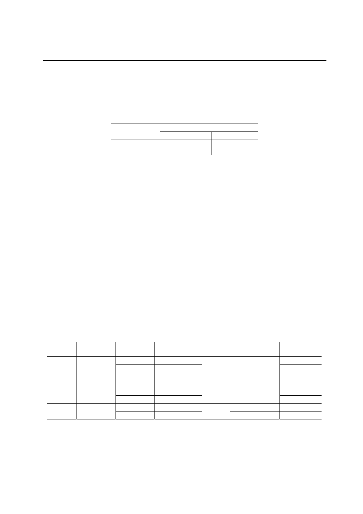
1.1.3 Setting Input System Write Enable and Read Enable
This IC generates the write enable signals (IWE) for writing data in the valid area made up of the valid vertical
lines and the valid horizontal pixels defined by the input control mode settings to the write port of the frame
memory.
With the write enable, it is possible to set the starting point in the vertical and horizontal directions. This setting
makes it possible to position the areas of valid lines and valid pixels with non-standard phase Sync. signals.
This IC also generates a Read Enable (IRE) signal for Read operation to establish recursive noise reduction.
By setting PAOS (SUB:72h-bit[4]) to 1, the valid start offset, which is 2 lines at the setting of INPR=0 and 4 lines
at the setting of INPR=1, is set and the number of valid lines is reduced by 2 lines or 4 lines from the normal
condition.
Table F1-1-3(1) Valid Input Data Area (INPR=0: Interlace)
VMD HMD
[1] [0] [1] [0]
0 0 0 0 288(286) 720
0 1 0 0 243(241) 720
0 0 0 1 288(286) 768
0 1 0 1 243(241) 640
0 0 1 0 288(286) 768
0 1 1 0 243(241) 768
Other than above Test modes (not settable)
Valid lines Valid pixels
Table F1-1-3(2) Valid Input Data Area (INPR=1: Progressive)
VMD HMD
[1] [0] [1] [0]
0 0 0 0 576(572) 720
0 1 0 0 486(482) 720
0 0 0 1 576(572) 768
0 1 0 1 486(482) 640
0 0 1 0 576(572) 768
0 1 1 0 486(482) 768
Other than above Test modes (not settable)
Valid lines Valid pixels
15/123
PEDL87V21071-01
OKI Semiconductor
IHS
IWE
IRE
YI
CI
IHS
IWE
IRE
YI
CI
243/288/486/576lines
: Valid data : Invalid data
Figure F1-1-3(1) Input Vertical Valid Lines
720/640/768pixels
: Valid data : Invalid data
Figure F1-1-3(2) Input Horizontal Valid Pixels
ML87V21071
16/123
PEDL87V21071-01
OKI Semiconductor
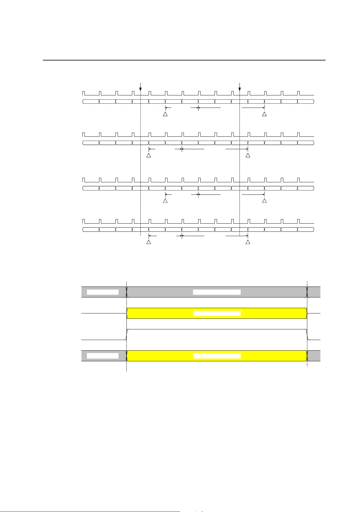
• Setting of Input System Vertical Valid Line Start Position
The input system vertical valid line start position (IVPS) is set in line unit with reference to the input system
vertical reset (IVR: internal signal ), generated from IVS, by setting N PVWE[4:0] (SUB :44h-bit[4:0]) . Data of
valid lines is written in the memory taking the input data subsequent to IVPS as valid data.
For this value, ±7 lines (15 stages) can be set for the reference position (NPVWE[3:0]=8h) in interlace mode
(INPR=0) and in progressive mode (INPR=1), ±15 lines (31 stages) can be set for the reference position
(NPVWE[4:0]=10h).
In interlace mode, NPVWE[4] is ignored.
Table F1-1-3 (3) Input System Vertical Valid Line Start Position (INPR=0: Interlace)
R656I
0 0 0 13 (–7 lines)
0 0 1 7 (–7 lines)
1 0 0 17 (–7 lines) (*1)
1 0 1 12 (–7 lines) (*1)
Other than above Test modes (not settable)
*1: In the case of field B, it is +1.
VMD IVPS position (number of IHS’s from IVR)
[1] [0] NPVWE=1h
……
……
……
……
……
NPVWE=8h
20 (default)
14 (default)
24 (default) (*1)
19 (default) (*1)
……
……
……
……
……
NPVWE=Fh
27 (+7 lines)
21 (+7 lines)
31 (+7 lines) (*1)
26 (+7 lines) (*1)
Table F1-1-3 (4) Input System Vertical Valid Line Start Position (INPR=1: Progressive)
R656I
0 0 0 24 (–15 lines)
0 0 1 12 (–15 lines)
VMD IVPS position (number of IHS’s from IVR)
[1] [0] NPVWE=1h
……
……
……
NPVWE=10h
49 (default)
27 (default)
……
……
……
NPVWE=1Fh
54 (+15 lines)
42 (+15 lines)
IVS
7 lines7 lines
ML87V21071
IHS
#IVR
#IWE/IRE
YI[7:0]
CI[8:0]
IVS
IHS
#IVR
#IWE/IRE
YI[7:0]
CI[8:0]
IVPS
288/243 lines
: Valid data #: Internal signal
Figure F1-1-3 (3) Input System Vertical Valid Line Start Timing (INPR=0)
15 lines15 lines
IVPS
576/486 lines
: Valid data #: Internal signal
Figure F1-1-3 (4) Input System Vertical Valid Line Start Timing (INPR=1)
17/123
PEDL87V21071-01
OKI Semiconductor
ML87V21071
• Setting of Input System Horizontal Valid Pixel Start Position
The input system horizontal valid pixel start position (IHPS) is set in pixel unit with reference to the input
system horizontal reset (IHR: internal signal), generated from IHS, by setting NPHWE[7:0]
(SUB:45h-bit[7:0]).
The data subsequent to IHPS is written in the data memory of valid pixels as the valid data.
This value can be set in 255 levels of ±127 pixels with regard to the initial value (NPHWE[7:0] = 80h).
In the ITU-R BT.656 mode, the value cann ot be set. Wri te enable with regard to valid data is generated on the
basis of detected SAV, EAV.
Table F1-1-3 (5) Input System Horizontal Valid Pixel Start Position
HMD IHPS position (Number of pixels from IHS)
[1] [0]
0 0 0 17 (–127 pixels)
0 0 1 11 (–127 pixels)
0 1 0 49 (–127 pixels)
0 1 1 13 (–127 pixels)
1 0 0 49 (–127 pixels)
1 0 1 15 (–127 pixels)
Other than above Test modes (Setting inhibited)
VMD
[0]
NPHWE=01h
……
……
……
……
……
……
……
NPHWE=80h
144 (default)
138 (default)
176 (default)
140 (default)
176 (default)
142 (default)
……
……
……
……
……
……
……
NHPWE=FFh
271 (+127 pixels)
265 (+127 pixels)
303 (+127 pixels)
267 (+127 pixels)
303 (+127 pixels)
269 (+127 pixels)
127 pixels127 pixels
IHS
IHPS
#IWE
1 pixel
YI[7:0]
CI[7:0]
640/720/768 pixels
1 pixel
Valid data
Figure F1-1-3 (5) Input System Horizontal Valid Pixel Start Timing
18/123
PEDL87V21071-01
[
]
[
]
OKI Semiconductor
ML87V21071
1.1.4 Input System Sync. Signal Polarity Inversion Setting
Negative polarity IVS can also be supported by setting the I
2
C-bus setting register IVSINV (SUB:42h-bit[0]).
Moreover, with regard to field detection, setting is possible even when setting the internal IVR generation edge.
Table F1-1-4 (1) IVINV Setting
IVSINV Recommended input IVS polarity IVR generation edge
0 Positive (default) Rising edge
1 Negative Falling edge
IVSINV=1IVSINV=0
IVS
IWE
Value set by
NPVWE[3:0]
IVS
IWE
Value set by
NPVWE[3:0]
Figure F1-1-4 (1) Support of Input System Vertical Sync. Signal Polarity Inversion
Negative polarity IHS can also be supported by setting the I
2
C-bus setting register IHSINV (SUB:42h-bit[1]).
Table F1-1-4 (2) IHSINV Setting
IHSINV Input IHS polarity
0 Positive (default)
1 Negative
IHSINV=1IHSINV=0
IHS
IWE
Value set by
NPHWE
7:0
IHS
IWE
Value set by
NPHWE
Figure F1-1-4 (2) Support of Input System Horizontal Sync. Signal Polarity Inversion
7:0
19/123
PEDL87V21071-01
OKI Semiconductor
ML87V21071
1.1.5 Input System Detection Field Inversion Setting
Inversion of input system internal field detection is possible by setting IFINV (SUB:42h-bit[2]) by I
interface. However, setting is not necessary if there is no problem in normal detection.
Table F1-1-5 IFIND Setting
IFINV
0 0 1
1 1 0
Field A Field B
Input field
* PAL : Field A = 1st, 3rd, 5th, 7th color field
Field B = 2nd, 4th, 6th, 8th color field
* NTSC : Field A = 2nd, 4th color field
Field B = 1st, 3rd color field
1.1.6 Input System Vertical Reset Compensation Mode Setting
In this IC, the rear edge (in the case of standard signal, 625 lines; A-3 line, 0.5H position, in between B-315 an d
B-316 lines, 525 lines; A-6 line, 0.5H position, in between B-6 and B-7 lines) of normally standard vertical Sync.
signal (IVS) is regarded as the reference position (IVR generating position) to perform field detection and
memory control.
If a Sync. signal with unspecified phase of the IVS rear edge and horizo n t al Sy nc. signal (IHS) is input, the front
edge can be used with the setting IVSINV = 1. But if the front edge is used in standard 626-line mod e, the
detection filed reverses in normal operation and field B gets written in the memory with one line earlier phase.
Therefore, by setting the I
2
C-bus setting register IVEM (SUB:42h-bit[4]), the detection field is inve rted (A→B,
B→A) and the vertical phase with regard to field B of the inverted result is delayed by 1H.
This allows compensation for field detection and IVR which is the typical front edge phase of IVS of 625-line
mode.
In practice, this allows compliance with the Sync. signal examples shown in Table F1-1-6 and Figure F1-1-6.
Note: Use it in case the phase of field-detecting IVS and IHS reverses in the IC standard setting.
Table F1-1-6 Input System Vertical Reset Compensation by IVEM Setting
Condition
Phase 1
Phase 2
Phase 3
Phase 4
Vertical
reference
Rear edge
IVSINV = 0
Rear edge
IVSINV = 0
Front edge
IVSINV = 1
Front edge
IVSINV = 1
Input
data field
A A n
B B
A B A n
B A
A A n
B B
A B A n
B A
Internal
decision field
IVEM
setting
0 No compensation
1
0 No compensation
1
Field after
compensation
B n + 1
B n + 1
Valid data start
position
n
n
2
C-bus
20/123
PEDL87V21071-01
OKI Semiconductor
Input sync signal phase 1
Field A input
IHS
IVS
#IVR
#IF
Field B input
IHS
IVS
#IVR
#IF
Input sync signal phase 2
Field A input
IHS
IVS
#IVR
#IF
0 1 2 nn-1
0 1 2 nn-1
ML87V21071
Input sync signal phase 3
nn-10 1 2
Input sync signal phase 4
IHS
IVS
#IVR
#IF
IHS
IVS
#IVR
#IF
IHS
IVS
#IVR
#IF
Field A input
0 1 2 nn-1
Field B input
Field A input
0 1 2 nn-1
3 4 5
3 4 5
3 4 5
nn-10 1 2
IHS
IVS
#IVR
#IF
Field B input
nn-10 1 2 n+1
IHS
IVS
#IVR
#IF
Field B input
3 4 5
nn-10 1 2 n+1
Figure F1-1-6 Input System Vertical Reset Compensation by IVEM Setting
21/123
PEDL87V21071-01
OKI Semiconductor
ML87V21071
1.1.7 Stop Memory Write Setting (Freeze Function)
By setting the I
2
C-bus settings register STL[2:0] (SUB:43h-bit[2:0]), you can stop writing data to the memory.
When you do this, the noise reduction feature stops.
Further, by setting STLM[1:0] (SUB:43h-bit[4:3]), field still image output, frame still image output, or frame still
median) image output can be selected.
The still image data output is achieved by rewriting only the signals read from the memory for the valid data
period selected by the IBLK signal, which indicates the valid data. Therefore, it is necessary to input the input
Sync. signals as normal.
The data output as a field or frame (median) still image is based on the most recent data written to the memory
(before the writing was stopped).
The timing of the writing stop and restoration can be set in one of the following three modes: selected field A/B
timing, field A timing, and field B timing.
In the mode of selected field A/B timing, writing is stopped after data for the next frame (field A + field B) after
writing stop is set is written. Writing is restored from the next frame after writing restoration is set. In this mode,
the field still image output depends on the writing stop setting timing.
In the mode of field A timing, after data for one frame (field B + field A) is written from the field B after writing
stop is set, writing is stopped from the next field B vertical Sync. signal. Writing is restored with the field B
vertical Sync. signal. In this mode, field A is always output for the field still image output.
In the mode of field B timing, after data for one frame (field A + field B) is written from the field A after writing
stop is set, writing is stopped from the next field A vertical Sync. signal. Writing is restored with the field A
vertical Sync. signal. In this mode, field B is always output for the field still image output.
When INPR is set to 1, the setting of field timing STL[2:1] is ignored and only STL[0] stop operation is
performed.
Table F1-1-7(1) Writing Stop Settings
STL
[2] [1] [0]
0 0 0 Possible (field A restoration)
0 1 0 Possible (field B restoration)
1 X 0 Possible (either field restoration)
0 0 1 Stopped (field A maintained)
0 1 1 Stopped (field B maintained)
1 X 1 Stopped (either field output maintained)
Input data writing
Table F1-1-7 (2) Still Image Output Mode Settings
STLM
[1] [0]
0 X Field image
1 0 Frame image
1 1 Frame image (median)
Output still image
22/123
PEDL87V21071-01
OKI Semiconductor
[Field A timing setting example 1]
IVS
Field
[Field A timing setting example 2]
IVS
Field
[Field B timing setting example 1]
IVS
Field
[Field B timing setting example 2]
IVS
Field
Writing stop set
A B
A B
A B A B A B A B A B A B
Writing stop processing
A B
A B A B A B A B A B A B
A B A B A B A B A B AB
Writing stop processing
start position
Writing stop processing
A B A B A B A B A B A B
Writing stop processing
start position
start position
Frame for pre-stop
write processing
start position
Frame for pre-stop
write processing
Frame for pre-stop
write processing
Frame for pre-stop
write processing
Stopping period
Stopping period
Writing restoration set
Stopping period
Writing stop processing
end position
Stopping period
Writing stop processing
end position
Writing stop processing
Writing stop processing
Figure F1-1-7 (1) Writing Stop/Restoration Timing
ML87V21071
end position
AB
end position
Input data
Memory data
Valid dataBLK data
Valid data
#IBLK
Output data
BLK data Valid data
Figure F1-1-7(2) Output Data in Still Image Mode
* When MEM411 is set to 1, output data from the memory is converted to 4:2:2 data (pseudo conversion) through
linear interpolation of c hrom inance data si nc e the o utput da t a is 4:1: 1 data . The refore , t he ban d o f t he da ta on t he
chrominance side deteriorates from that of the normal data.
23/123
PEDL87V21071-01
OKI Semiconductor
ML87V21071
1.2 Input/Output Format
1.2.1 Input Data Format
The input of this IC complies with 16-bit 4:2:2 (YI[7:0] = Y-8bit, CI[7:0] = CbCr-8bit 4:2:2) format (input in
16-bit mode), 8-bit 4:2:2 (YI[7:0] = YCbCr-8bit 4:2:2, without SAV, EVA) format (input in 8-bit mode) and
ITU-R BT.656 conforming (YI[7:0] = YCbCr-8bit 4:2:2, with SAV, EAV) format (ITU-R BT.656 mode).
However, when INPR is set to 1, neither 8-bit input mode nor ITU-R BT.656 input mode can be selected.
The input format mode is set by an exte rnal pin MODE 2 or I
R656 (SUB:41h-bit[1]).
Switching of an external pin and a register is accomplished by setting the I
2
C-bus setting register DISEL (SUB: 4 1h -bit[0]), or
2
C-bus setting register IRMON
(SUB:40h-bit[7]).
Table F1-2-1 (1) Input Data Format Mode
IRMON MODE2 DISEL R656I Mode
0 0 X 0
1 X 0 0
0 1 X 0
1 X 1 0
X X X 1 ITU-R BT.656 mode
Input in 16-bit mode
Input in 8-bit mode
Table F1-2-1(2) Input Data Format
Input pin Input in 16-bit mode
YI7 Y07 Y17 Cb07 Y07 Cr07 Y17
YI6 Y06 Y16 Cb06 Y06 Cr06 Y16
YI5 Y05 Y15 Cb05 Y05 Cr05 Y15
YI4 Y04 Y14 Cb04 Y04 Cr04 Y14
YI3 Y03 Y13 Cb03 Y03 Cr03 Y13
YI2 Y02 Y12 Cb02 Y02 Cr02 Y12
YI1 Y01 Y11 Cb01 Y01 Cr01 Y11
YI0 Y00 Y10 Cb00 Y00 Cr00 Y10
CI7 Cb07 Cr07 — — — —
CI6 Cb06 Cr06 — — — —
CI5 Cb05 Cr05 — — — —
CI4 Cb04 Cr04 — — — —
CI3 Cb03 Cr03 — — — —
CI2 Cb02 Cr02 — — — —
CI1 Cb01 Cr01 — — — —
CI0 Cb00 Cr00 — — — —
Y point 0 1 0 1
C point 0 0
Input in 8-bit mode
ITU-R BT.656 mode
24/123

PEDL87V21071-01
OKI Semiconductor
Input in 8-bit mode or ITU-R BT.656 modeInput in 16-bit mode
ICLK
#IICLK #IICLK
YI[7:0]
CI[7:0]
#: Internal signal
Yn Yn+1 Yn+2 Yn+3
Cn Cn+1 Cn+2 Cn+3
ICLK
YI[7:0]
CI[7:0]
Cbn Yn Crn Yn+1
Figure F1-2-1 (1) Input Data Timing
The data and control signal interfaces according to input system modes are as follows.
• Input in 16-bit mode
Vertical Sync. signal: IVS
Horizontal Sync. signal: IHS
Data input pin: YI[7:0], CI[7:0] (YCbCr-4:2:2)
Input system clock frequency: f
= 12.2727272/13.5/14.31818/14.75 MHz
ICLK
Clip level: None
• Input in 8-bit mode
Vertical Sync. signal: IVS
Horizontal Sync. signal: IHS
Data input pin: YI[7:0], (YCbCr-4:2:2)
Input system clock frequency: f
= 24.545454/27/28.63636/29.5 MHz
ICLK
Clip level: None
• ITU-R BT.656 mode
Vertical Sync. signal: SAV, EAV split
Horizontal Sync. signal: SAV, EAV split
Data input pin: YI[7:0] (YCbCr-4:2:2)
Input system clock frequency: f
= 27 MHz
ICLK
Clip level: 00h → 01h, FFh → Feh
* By setting POFF (SUB:41h-bit[6]) to 1, the parity bits of SAV and EAV can be disabled.
ML87V21071
don't care (no connect)
25/123
PEDL87V21071-01
OKI Semiconductor
• Internal Input System Clock (IICLK)
The IICLK is IICLK = ICLK in 16-bit 4:2: 2 mode whereas in 8-bi t 4:2:2 mode and IT U-R BT.656 mode
it is the clock pulse obtained by internally frequency-dividing ICLK to 1/2.
In 8-bit 4:2:2 mode, the position which is two ICLK clocks delayed from the rise of IHS is used for
resetting and IICLK is generated by frequency-dividing ICLK to 1/2.
Normally reset of IICLK presumes the rise position of positive polarity IHS (IHSINV = 0), but by setting
IHES (SUB:41h-bit[5]) and IHSINV, selection of compliance with negative polarity IHS and fall
position is also possible.
In ITU-R BT 656 mode, ICLK is frequency-divided to 1/2 based on SAV.
In 8-bit 4:2:2 mode, if the p hase of IHS for l umina nce and chrominance d ata reverses (n umber of ICL Ks
from IICLK reset to initial chrominance data is odd), it is possible to avoid the reversal by setting ICINV
(SUB:41h-bit[4]).
Table F1-2-1 (4) Compliance with Luminance-Chrominance Phase Reversal
ICINV Usage conditions (8-bit 4:2:2 mode)
8-bit 4:2:2 mode
ICLK
IHS
IICLK
Reset
IICLK
YI[7:0]
Table F1-2-1 (3) IICLK Reset Position
IHES IHSINV Reset position
0 0
1 0
0 1
1 1
0 Number of ICLKs from IICLK reset to initial chrominance data is even.
1 Number of ICLKs from IICLK reset to initial chrominance data is odd.
Positive polarity IHS rise (horizontal Sync. signal front
edge)
Positive polarity IHS fall (horizontal Sync. signal rear
edge)
Negative polarity IHS fall (horizontal Sync. signal front
edge)
Negative polarity IHS rise (horizontal Sync. signal rear
edge)
Crn Yn Cbn Yn+1
Figure F1-2-1 (2) IICLK Phase Timing Example
ML87V21071
26/123
PEDL87V21071-01
OKI Semiconductor
ML87V21071
1.2.2 Output Data Format
Since internal signal processing is performed independently for luminance and chrominance signals, the output
data format of basic output of this IC is YCbCr 16bit 4:2:2.
However, in YCbCr 8bit 4:2:2 mode and ITU-R BT.656 mode, selection of YCbCr 8bit 4:2:2 (same format as
input) is enabled by setting DOSEL (SUB:60h-bit[1]) to 1. In this case, unused CO[7:0] becomes Hi-Z.
Table F1-2-2(2) shows the delay amount from input to output and the same delay amount occurs for all the data
and Sync. signals.
Table F1-2-2 (1) Output Data Format
Output Normal mode 8-bit input – 8-bit output mode (DOSEL =1)
YO7 Y07 Y07 Cr07 Y17 Cb07 Y17
YO6 Y06 Y06 Cr06 Y16 Cb06 Y16
YO5 Y05 Y05 Cr05 Y15 Cb05 Y15
YO4 Y04 Y04 Cr04 Y14 Cb04 Y14
YO3 Y03 Y03 Cr03 Y13 Cb03 Y13
YO2 Y02 Y02 Cr02 Y12 Cb02 Y12
YD1 Y01 Y01 Cr01 Y11 Cb01 Y11
YD0 Y00 Y00 Cr00 Y10 Cb00 Y10
CO7 Cb07 Cr07 — — — —
CO6 Cb06 Cr06 — — — —
CO5 Cb05 Cr05 — — — —
CO4 Cb04 Cr04 — — — —
CO3 Cb03 Cr03 — — — —
CO2 Cb02 Cr02 — — — —
CO1 Cb01 Cr01 — — — —
CO0 Cb00 Cr00 — — — —
Table F1-2-2(2) Combinations for Input/Output Data Format
DISEL R656I DOSEL Input Output
0 0 X 16-bit + Sync (H, V) 16-bit + Sync (H, V) 32 (ICLK)
1 0 0 8-bit + Sync (H, V) 8-bit + Sync (H, V) 64 (ICLK)
1 0 1 8-bit + Sync (H, V) 8-bit + Sync (H, V) 66 (ICLK)
X 1 0 ITU-R BT.656 16-bit + Sync (H, V) 64 (ICLK)
X 1 1 ITU-R BT.656 ITU-R BT.656 + Sync (H, V) 66 (ICLK)
Input/output delay
amount
* When input is ITU-R BT.656, Sync (H, V) on the output side is output to OVS and OHS as the Sync. signal
separated from SAV and EAV.
27/123
PEDL87V21071-01
OKI Semiconductor
ICLK
YI[7:0]
CI[7:0]
YO[7:0]
CO[7:0]
ICLK
YI[7:0]
ML87V21071
Y0 Y1
Cb0 Cr0
32(ICLK)
Y0 Y1 Y2
Cb0 Cr0 Cb1
Figure F1-2-2(1) Input/Output Delay in 16-Bit Input Mode
Cb0 Y0 Cr0 Y1
[DOSEL=0]
YO[7:0]
CO[7:0]
[DOSEL=1]
YO[7:0]
ICLK
YI[7:0]
[DOSEL=0]
YO[7:0]
CO[7:0]
[DOSEL=1]
64(ICLK)
Y0 Y1 Y2
Cb0 Cr0 Cb0
66(ICLK)
Cb0 Y0 Cr0 Y1
Figure F1-2-2(2) Input/Output Delay in 8-Bit Input Mode
FF 00 00 SAV Cb0 Y0 Cr0 Y1
64(ICLK)
00 SAV Y0 Y1 Y2
FF 00 Cb0 Cr0 Cb0
66(ICLK)
YO[7:0]
FF 00 00 SAV Cb0 Y0 Cr0 Y1
Figure F1-2-2(3) Input/Output Delay in ITU-R BT.656 Mode
28/123
PEDL87V21071-01
OKI Semiconductor
ML87V21071
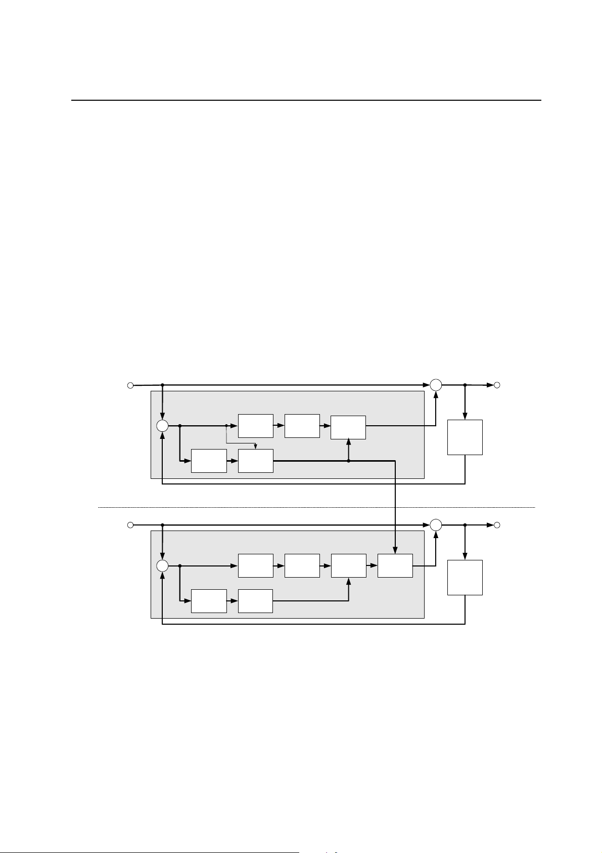
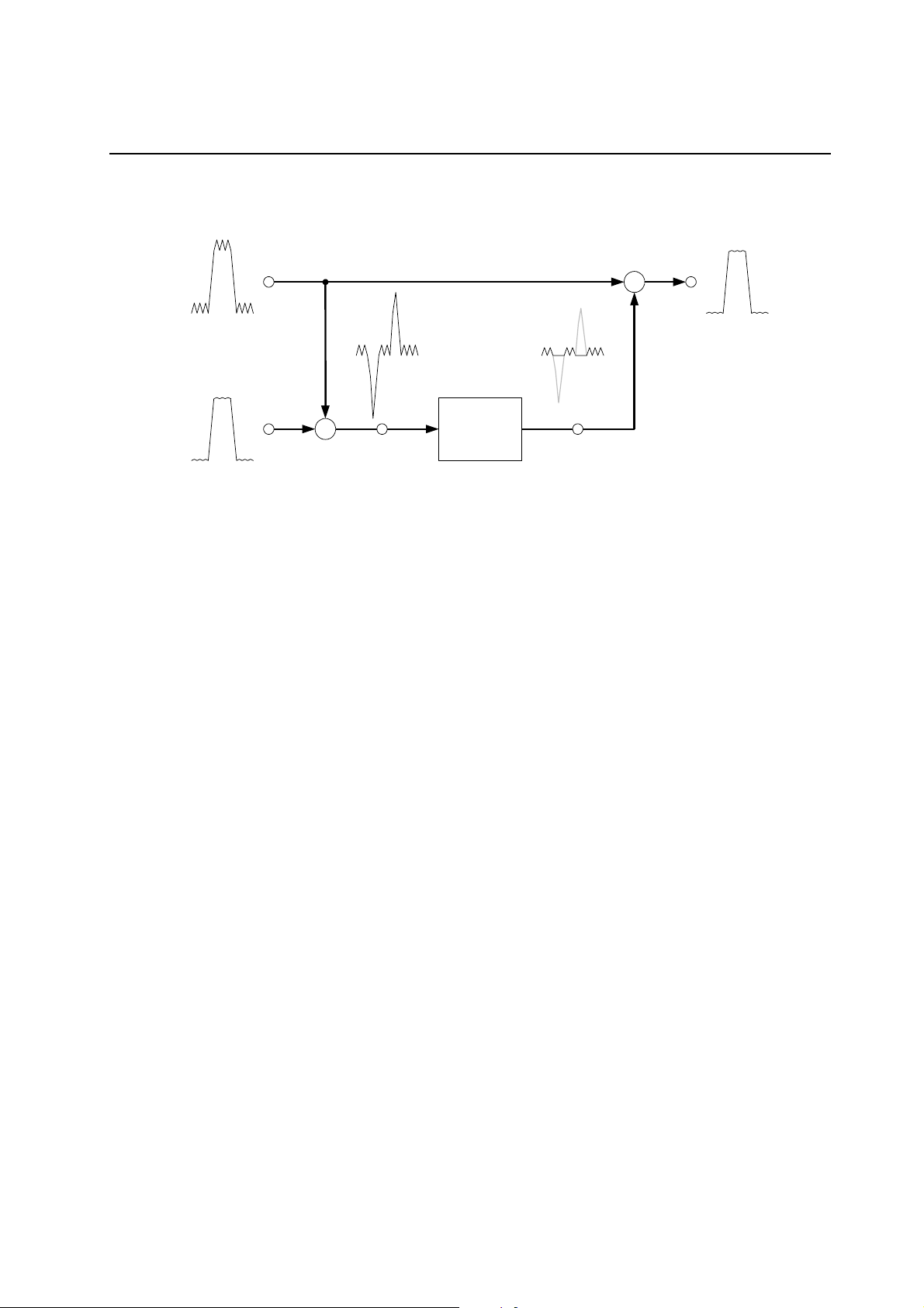
2. Video Signal Processing Functions
2.1 Motion-Adaptive 3D Noise Reduction
This IC performs noise reduction first by detecting noise and predicting motion using frame recursion, field
recursion, and line correlation, then by performing noise subtraction while performing motion compensation for
the detected noise. Moreover, it achieves adaptive noise reduction by synthesizing four NR data items based on
prediction of motion.
However, when INPR is set to 1, the field recursion stops and adaptive noise reduction is performed by the two
NR data items, frame recursion and line correlation.
• Principle of Noise Reduction
Difference between the current field data and the filed data preceding one frame, one field, or one line is
extracted as time motion and noise independently for luminance and chrominance signals.
The low gain portion of this data is judged to be noise and the high gain portion to be motion an d is extrac ted
as motion level detection noise.
The noise component extracted here is subjected to motion prediction by ad jacent motion level and adjacent
code, then further subjected to c om pensati on base d on m otion a nd i s regarde d as the fina l noi se component.
Finally, noise reduction is carried out by subtracting this final noise data from the current field data.
Luminance
input data
Luminance noise detection
+
-
-
LPF
MSB
Non-
linear filter
Motion
detection
Limiter
Motion
compen-
sation
+
-
-
Field
memory
NR recursive data
Luminance
output data
Chrominance
input data
+
-
-
Chrominance noise detection
+
-
-
LPF
Non-
linear filter
Motion
detection
Limiter
Chrominance
motion level
compen-
sation
Luminance
interlock
motion
compensation
Field
memory
Figure F2-1 (1) Noise Detection Type Noise Reduction Configuration
Chrominance
output data
NR recursive data
29/123
PEDL87V21071-01
Noi
OKI Semiconductor
Current field data
One preceding field data
–
–
se
–
–
detection
+
motion
compensation
Figure F2-1(2) Noise Reduction by Noise Detection
ML87V21071
Data after 3DNR
30/123

PEDL87V21071-01
OKI Semiconductor
ML87V21071
• Principles of Adaptive Noise Reduction
Adaptive noise reduction is achieved through the selection of noise reduction data, which utilizes the
correlative relationships between frames, fields, and lines for the pixels for which noise reduction is to be
performed, as shown in Figure F2-3 (3).
The distinguishing characteristics of each correlation are as shown below.
Between frames : Same position (most effective), time difference 2V (less effective)
→Effective for still images (good NR, substantial afterimage)
Between fields : Position 0.5H different (effective), time difference 1V(effective)
→More effective for moving images than frames, more effective for still images than
lines (medium NR, medium afterimage)
Between lines : Position 1H different (less effective), time difference 0 (most effective)
→Effective for moving images, but not effective for edges (medium NR, no
afterimage, no NR for edges)
This IC detects motions and e dges betwee n lines, f rames, and fields, ba sed on t he features described a bove, t o
select data after better correlated NR and achieve effective noise reduction.
Time axis
2V
Direction of V
1V 1V
1H
: NR-target pixel
: NR
Figure F2-1 (3) Noise Reduction Correlation
31/123

PEDL87V21071-01
OKI Semiconductor
ML87V21071
2.1.1 Noise Reduction Mode
The noise reduction mode is set by NR2OFF(SUB:48h-bit[4]), FNRM[1:0] (SUB:48h-bit[6:5]), and you can
select the noise reduction modes shown in Table F2-1-1.
Synthesis of an adaptive noise reduction mode is performed by checking motions that are predicted from the
motion detection signal and differe ntial sign al level that are detected at noi se reducti on between frames, fiel ds, or
lines.
For determining the motion difference level, weighting factor can be applied to frames by setting the adaptive
margin that is set by YFAM(SUB:4Ah-bit[1]), CFAM(SUB:4Bh-bit[1]). NR effect is improved by applying
weighting factor to frames (however, afterimage will be more likely to occur).
Table F2-1-1 (1) Noise Reduction Modes
FNRM
[1] [0]
0 0
0 0 1 3D adaptive frame-recursive NR (uses frames and fields)
0 1 0 2D adaptive frame-recursive NR (uses frames and lines)
0 1 1 Frame-recursive NR
1 X 0 2D adaptive field-recursive NR (uses fields and lines)
1 X 1 Field-recursive NR
NR2OFF Noise Reduction Mode
0
Fully adaptive frame-recursive NR (uses frames, fields, and
lines)
Table F2-1-1 (2) Luminance Adaptive Margin Settings
YFAM
0 0
1 –2
Luminance adaptive
margin
Remarks
Frame NR performance emphasized (larger
NR, larger afterimage)
F2-1-1 (3) Chrominance Adaptive Margin Settings
CFAM
0 0
1 –2
Chrominance adaptive
Margin
Remarks
Frame NR performance emphasized (larger
NR, larger afterimage)
32/123

PEDL87V21071-01
OKI Semiconductor
ML87V21071
2.1.2 Detected Noise Between Frames, Fields and Lines
The differences are calculated between
- one pixel in the current field and one pixel preceding by one frame,
- one pixel in the current field and two pixels by one field, and
- one pixel in the current field and one pixel preceding by one line.
Among the absolute values of these differences, the smallest value is selected.
From the differential values between frames and between fields (∆Y, ∆C), the signal with a low level of absolute
value for the differential values (|∆Y|, |∆C|) is judged to be the noise component and the signal with a high level is
judged to be the motion component. The data judged to be the noise is extracted as the motion level detection
noise.
The detected noise is output after being filtered by the area covered by the input noise detectio n line, the noise
convergence line, and the noise upper limit line. The inclination of the input noise detection line is set by
YSLT[1:0](SUB:4Ah-bit[5:4]) and CSLT[1:0](SUB:4Bh-bit[5:4]), the inclination and offset of the noise
convergence line are set by YSLT[3:2](SUB:4Ah-bit[7:6]), YNS[5:0] (SUB:4Ch-bit[5:0]), CSLT[3:2]
(SUB:4Bh-bit[7:6]) and CNS[5:0] (SUB:4Dh-bit[5:0]), and the offset of the noise upper limit line, which has 0
inclination, is set by YLM[4:0] (SUB:4Eh-bit[4:0]) and CLM[4:0] (SUB:4Fh-bit[4:0]). (Figure F2-1-1)
Table F2-1-2 Non-Linear Filter Noise Detection Area Settings
YSLT/CSLT Noise detection line Noise convergence line Noise upper limit line
[3] [1] [2] [0] Inclination Offset Inclination Offset Inclination Offset
0 0 0 0 1
0 0 0 1 7/8
0 1 0 0 3/4
–1
0 1 0 1 1/2
0 0 1 0 1
0 0 1 1 7/8
0 1 1 0 3/4
0 1 1 1 1/2
1 0 0 0 1
1 0 0 1 7/8
1 1 0 0 3/4
0
–3/4
–1/2
YNS[5:0]
CNS[5:0]
0
YLM[4:0]
CLM[4:0]
1 1 0 1 1/2
1 0 1 0 1
1 0 1 1 7/8
1 1 1 0 3/4
–3/2
1 1 1 1 1/2
Field-recursive
detection noise
output
31(MAX)
Noise convergence line
Input noise detection line inclination
1 or 7/8 or 3/4 or 1/2
Noise detection line
Non-noise detection area
Noise convergence line inclination
-1 or -3/4 or -1/2 or -3/2
Noise upper limit line
Noise upper limit
line offset:
YLM[4:0], CLM[4:0]
= 0 to 31
Noise detection area
(Differential absolute
0
Noise convergence line offset: YNS[5:0], CNS[5:0] = 0 to 63
63(MAX)
value of difference
between fields
|∆Y|, |∆C|) input
Figure F2-1-2 Field-Recursive Noise Motion Level Detection Noise Characteristics
33/123

PEDL87V21071-01
OKI Semiconductor
ML87V21071
2.1.3 Detection of Motion between Frames, Fields, and Lines
There are two types of luminance signal motion detection: level motion detection and continuous code motion
detection.
Chrominance signal motion detection includes level motion detection.
c Luminance Level Motion Detection
From the differential data between fields, including luminance signal motion and noise, the high frequency
component (∆HY) is filtered with the LPF, extracting only the low frequency differential data (∆LY).
Luminance LPF: F(z) = (1/8)z
-2
+ (1/8)z-1 + (1/2)z0 + (1/8)z1 + (1/8)z2
The low frequency differential data is assumed to have a large proportion of the motion component, so the
absolute value of that data (|∆LY|) is compared with the luminance noise convergence level set in YNS[5:0] to
determine the amount of motion.
If the result shows that the differential absolute value is greater than the noise convergence level, it is determined
that there is a lot of motion in the data, and the motion flag (YMT) = 1 is set.
If the differential absolute value is less than the noise convergence level, it is determined that there is not much
motion in the data, and the motion flag (YMT) = 0 is set.
Table F2-1-3 (1) Luminance Level Motion Detection
Motion Detection Conditions Motion Flag (YMT)
|∆LY| > 64
|∆LY| > YNS[5:0]
|∆LY| ≤ YNS[5:0]
1
1
0
d Luminance Continuous Code Motion Detection
This feature detects sequences of 3, 4, and 5 continuous codes in the differential data that includes the pixels for
which noise detection is being performed. Where continuity is detected, the absolute value of the low frequency
differential data and the continuous code motion detection level YMS[3:0]( SUB:50h-bit[3:0]) are compared to
determine the amount of motion.
• 3 Continuous Code Detection
If 3 continuous codes are detected to be the same and their low frequency differential data absolute values are
equal to or greater than the continuous code motion detection level (YMS[3:0]), the data is judged to have much
motion, and the 3 continuous code motion flag (YMT3) = 1 is set.
If the absolute value is less than the continuous motion detection level, the data is judged to have little motion, and
the 3 continuous code motion flag (YMT3) = 0 is set.
Table F2-1-3 (2) Luminance 3 Continuous Code Motion Detection
Motion detection condition Motion flag (YMT3)
|∆LY| > 16
|∆LY| ≥ YMS[3:0]
|∆LY| < YMS[3:0]
1
1
0
34/123

PEDL87V21071-01
OKI Semiconductor
ML87V21071
• 4 Continuous Code Detection
If 4 continuous codes are detected to be the same and their low frequency differential data absolute values are
equal to or greater than the continuous code motion detection level 1/2(YMS[3:1]), the data is judged to have
much motion, and the 4 continuous code motion flag (YMT4) = 1 is set.
If the absolute value is less than the continuous motion detection level, the data is judged to have little motion, and
the 4 continuous code motion flag (YMT4) = 0 is set.
By setting YMDM( SUB:50h-bit[4]) = 1, the detection precision of the 4-continu ous code motion flag can be
improved.
Table F2-1-3 (3) Luminance 4 Continuous Code Motion Detection
Motion detection condition Motion flag (YMT4)
|∆LY| > 8
|∆LY| ≥ YMS[3:1]
|∆LY| < YMS[3:1]
1
1
0
• 5 Continuous Code Detection
If 5 continuous codes are detected to be the same and their low frequency differential data absolute values are
equal to or greater than the continuous code motion detection level 1/4 (YMS[3:2]), the data is judged to have
much motion, and the 5 continuous code motion flag (YMT5) = 1 is set.
If the absolute value is less than the continuous motion detection level, the data is judged to have little motion, and
the 5 continuous code motion flag (YMT5)=0 is raised.
By setting YMDM( SUB:50h-bit[4]) = 1, the detection precision of the 5-continu ous code motion flag can be
improved.
Table F2-1-3 (4) Luminance 5 Continuous Code Motion Detection
Motion detection condition Motion flag (YMT5)
|∆LY| > 4
|∆LY| ≥ YMS[3:2]
|∆LY| < YMS[3:2]
1
1
0
e Chrominance Level Motion Detection
From the differential data between fields, including chrominance signal motion and noise, the high frequency
component (∆HC) is filtered with the LPF, extracting only the low frequency differential data (∆LC).
Chrominance LPF: F(z) = (1/4)z
-2
+ (1/2)z0 + (1/4)z2
The low frequency differential data is assumed to have a large proportion of the motion component, so the
absolute value of that data (|∆LC|) is compared with the chrominance noise convergence level set in CNS[5:0] to
determine the amount of motion.
If the result shows that the differential absolute value is greater than the noise convergence level, the data is
judged to have a lot of motion, and the chrominance motion flag (CMT) = 1 is set.
If the differential absolute value is less than the noise convergence level, it is determined that there is not much
motion in the data, and the motion flag (CMT) = 0 is set.
This motion flag is used in adjacent pixel motion compensation.
Table F2-1-3 (5) Chrominance Level Motion Detection
Motion detection condition Motion flag (CMT)
|∆LC| > 64
|∆LC| > CNS[5:0]
|∆LC| ≤ CNS[5:0]
1
1
0
35/123

PEDL87V21071-01
OKI Semiconductor
ML87V21071
2.1.4 Motion Compensation Processing
This IC performs the motion compensation descri bed below in c and d for the noise de tected in Section 2.1. 2 It
does this by creating the motion compensation flags YMA[3:0] and CMA[4:0] from the motion flags (YMT,
YMT3, YMT4, YMT5, and CMT) detected in Section 2.1.3, the motion compensation stop settings YMOFF[3:0]
(SUB:51h-bit[3:0]) and CMOFF[4:0](SUB:52h-bit[4:0]), and the luminance linked chrominance motion
compensation setting CMY (SUB:52h-bit[7]).
Table F2-1-4 (1) Motion Compensation Flags
Motion
compensation flag
YMA[0] YMT&YMOFF[0]
YMA[1] YMT&YMOFF[1]
YMA[2] YMT&YMOFF[2]
YMA[3] YMT&YMOFF[3]
CMA[0] CMT&CMOFF[0]
CMA[1] YMT&CMOFF[1]&CMY
CMA[2] YMT3&CMOFF[2]&CMY
CMA[3] YMT4&CMOFF[3]&CMY
CMA[4] YMT5&CMOFF[4]&CMY
Composite signal Remarks
Luminance adjacent pixel level luminance
motion compensation
Luminance 3 continuous codes luminance
motion compensation
Luminance 4 continuous codes luminance
motion compensation
Luminance 5 continuous codes luminance
motion compensation
Chrominance adjacent pixel level chrominance
motion compensation
Luminance adjacent pixel level chrominance
motion compensation
Luminance 3 continuous codes chrominance
motion compensation
Luminance 4 continuous codes chrominance
motion compensation
Luminance 5 continuous codes chrominance
motion compensation
c Luminance Signal Noise Motion Compensation
This feature performs motion compensation for the detected noise using the motion compensation flag
YMA[3:0].
As the method of motion compensati on , you can select the reductio n mode (YNRM = 0) o r the noise 0 mode with
YNRM(SUB:4Ah-bit[0]).
In the reduction mode, you can choose the normal reduction mode (YABN = 0) or the absolute noise reduction
mode (YABN = 1) in register YABN(SUB:4Ah-bit[2]).
Table F2-1-4 (2) Luminance Motion Compensation Modes
YNRM YABN
X X None Detected noise as is
0 0 Normal reduction
0 1 Absolute noise reduction
1 X Noise 0
Motion compensation
mode
Remarks
(Detected noise) x
(Reduction coefficient)
(Detected noise) x
(Reduction coefficient)
Noise 0 judgment
(NROFF)
36/123

PEDL87V21071-01
OKI Semiconductor
ML87V21071
Table F2-1-4 (3) Noise Reduction Coefficients
YMA Reduction coefficient
[3] [2] [1] [0] YABN = 0 YABN = 1
0 0 0 0 1 1
0 0 0 1 1/2 3/4
0 0 1 0 1/2 3/4
0 0 1 1 1/4 5/8
0 1 1 0 1/4 5/8
0 1 1 1 1/8 9/16
1 1 1 0 1/8 9/16
1 1 1 1 1/16 17/32
d Chrominance Signal Noise Motion Compensation
This feature performs mot ion compensation for t he detected noise using the motion com pensation flag CMA[ 4:0].
As the method of motion c ompensation , the reduct ion mode (CNRM = 0) or the noise 0 mode (CNRM = 1) can be
selected by CNRM (SUB:4Bh-bit[0]).
In the reduction mode, the normal reduction mode (CABN = 0) or the absolute noise reduction mode (CABN = 1)
can be selected by CABN (SUB:4Bh-bit[2]).
Table F2-1-4 (4) Chrominance Motion Compensation Mode
CNRM CABN Motion compensation mode Remarks
X X None Detected noise as is
0 0 Normal reduction
0 1 Absolute noise reduction
1 X Noise 0
(Detected noise) x
(Reduction coefficient)
(Detected noise) x
(Reduction coefficient)
Noise 0 judgment
(NROFF)
Table F2-1-4 (5) Chrominance Normal Reduction Mode Noise Reduction Coefficients
CMA Reduction coefficient
[4] [3] [2] [1] [0] CABN=0 CABN=1
0 0 0 0 0 1 1
0 0 0 0 1 1/2 3/4
0 0 0 1 0 1/2 3/4
0 0 0 1 1 1/4 5/8
0 0 1 0 0 1/2 3/4
0 0 1 0 1 1/4 5/8
0 0 1 1 0 1/4 5/8
0 0 1 1 1 1/8 9/16
0 1 1 0 0 1/4 5/8
0 1 1 0 1 1/8 9/16
0 1 1 1 0 1/8 9/16
0 1 1 1 1 1/16 17/32
1 1 1 0 0 1/8 9/16
1 1 1 0 1 1/16 17/32
1 1 1 1 0 1/16 17/32
1 1 1 1 1 0 1/2
37/123

PEDL87V21071-01
OKI Semiconductor
ML87V21071
2.1.5 Noise Reduction Stop Setting
Noise reduction can be forcibly stopped by setting NROFF (SUB:48h-bit[0]) on the I
2
C-bus interface.
However, data can be written into the memory even while noise reduction is stopped.
Table F2-1-5 NROFF Setting
NROFF Noise Reduction
0 Operated
1 Stopped
2.1.6 Noise Reduction Demo Mode Setting
By setting NRDEMO[2:0] (SUB:48h-bit[2:0]), a screen can be split as shown in Figure F2-1-6 and noise
reduction function can be confirmed as demo mode or the I
2
C-bus interface.
However, the demo mode does not work when noise reduction is stopped by setting NROFF = 1.
Table F2-1-6 NRDEMO Setting
NROFF
0 0 0 0 NR setting value NR setting value
1 X X X Stop NR Stop NR
0 X X 1 Stop NR NR setting value
0 X 1 0 NR Setting value Adaptive NR ON
0 1 0 0 NR Setting value
NRDEMO
[2] [1] [0]
Left side of screen Right side of screen
Adaptive line
correlation NR ON
Left side area
of screen
Right side area
of screen
Figure F2-1-6 Noise Reduction Demo Screen
38/123

PEDL87V21071-01
OKI Semiconductor
ML87V21071
2.1.7 Noise Status Detection
In order to automatically optimize noise reduction setting, this IC has a function for detecting the overall video
sample noise status during the motionless vertical blanking period.
• Detection of noise level (average and maximum values)
Set NRDTON (SUB:49h-bit[1]) = 1 to detect the blanking period noise level for one line (NDTC = 0) of a
vertical blanking period set by NRD TP[3:0] (SUB:57h -bit[4:2] ) and DT PSL (S UB:57h- bit[7]). Altern atively,
you can set the same register to detect the bl a nking noise (average and maxim um values) for one li ne ( NDTC
= 1) of the maximum noise level of multiple lines (a maximum of 16 lines not including valid lines) ending
with line NRDTP[2:0]. The detection of blanking period noise (average and maximum values) and the noise
on the line on which the average noise between fields for the valid data period is minimum can be performed
frame by frame.
The detection starting position is set in DTPSL. When DTPSL = 0, the starting position is immediately after
the end of the valid lines; when DTPSL = 1, the starting pos ition is one line after the end of the valid lines.
In a blanking period, one line is divided into two sections, the noise levels of the two sections are detected,
and the larger average noise value between the first 128 pixels and second 128 pixels is assumed as the
average value and maximum value of the line.
In a valid data period, one line is divided into four sections, the noise levels of the four 128-pixel periods are
detected, and the lowest average noise value is assumed as the a verage val ue a nd m axim um value of t he line.
During the valid data period, a luminance noise detection saturation level can be set through
PYST[1:0](SUB:52h-bit[6:5]), thereby preventing deterioration of the noise detection level by luminance
level saturation of CCD image input.
When NRDTON = 0, the final status data for NRDTON = 1 is preserved. Initially, the average and maximum
noise values are set at 0.
The fields for which detection is to be performed are set in NRDTF (SUB:49h-bit[5]). When NRDTF = 0,
field A vertical blanking period is set; when NRDTF = 1, field B vertical blanking period is set.
By setting YNMAS (SUB:57-bit[0]) and CNMAS (SUB:57h-bit[1]), it is possible to select either an 8-frame
average of the detected noise (YNMAS = 0, CNAMS = 0) or the level of detected noise in a single frame
(YNMAS = 1, CNAMS = 1).
For a noise detection area, a vertical blanking period, a valid data period, or a combination of both can be set
using PODT (SUB:49h-bit[4]) and PNON (SUB:49h-bit[7]).
39/123

PEDL87V21071-01
OKI Semiconductor
#Valid data
signal
NRDTP[3:0]
(DTPSL=0)
NRDTP[3:0]
(DTPSL=1)
#: Internal signal
Figure F2-1-7 (1) Vertical Blanking Noise Status Detection timing (NDTC = 0)
#Valid data
signal
NRDTP[3:0]
(DTPSL=0)
NRDTP[3:0]
(DTPSL=1)
IHS
IHS
1 2 3 4 5 14 15
0
1 2 3 4 5 13 14 150
NDTP[3:0]+1
NDTP[3:0]+1
ML87V21071
#: Internal signal
Figure F2-1-7 (2) Vertical Blanking Noise Status Detection timing (NDTC = 1)
40/123

PEDL87V21071-01
OKI Semiconductor
128pixels 128pixels
ML87V21071
Vertical blanking period
horizontal valid data
noize level detection per iod (2 x
128 pixels)
Vertical blanking
noise level detection
period (1 or 16 lines)
Vertical valid line
noise level detection period
128pixels128pixels128pixels128pixels
Valid data period
horizontal valid data
noize level detection per iod (2 x
128 pixels)
Figure F2-1-7(3) Noise Level Detection Area
41/123

PEDL87V21071-01
OKI Semiconductor
[NRDTF = 0: detection by field A]
Noise status
detection timing
[NRDTF = 1: detection by field B]
Noise status
detection timing
IVS
#IF
Field A
Field B
Field A
Figure F2-1-7 (4) Detection Field Based on NRDTF
Table F2-1-7 (1) Vertical Blanking Sample Noise Detection Settings
NRDTON Noise detection
0 Stopped (previously
detected data is maintained)
1 Operating
Table F2-1-7 (2) Noise Detection Field Settings
NRDTF Noise detection field
0 Field A
1 Field B
Table F2-1-7 (3) Blanking Period Noise Detection Line Settings
NDTC Noise detection line
0 1 line set at the NRDTP[3:0] position
1 Multiple lines (a maximum of 16 lines) from the line after the last
valid line to NRDTP[3:0]
Table F2-1-7 (4) Noise Detection Value Select Settings
YNAMS
CNAMS
0 Average of 8 frames
1 Single frame
Noise detection value
Table F2-1-7(5) Noise Detection Area Settings
PODT PNON Noise detection area
0 0 Vertical blanking only
0
1 X Valid data period only
Vertical blanking only + valid data
period
Table R2-1-7(6) Luminance Saturation Level Settings for Valid Data Area Noise Detection
PYST[1:0] Luminance saturation level
0h No saturation level
1h E0h
2h C0h
3h 80h
ML87V21071
Field B
42/123
PEDL87V21071-01
OKI Semiconductor
ML87V21071
c Detection of Basic Noise Status Signals
Detection of the basic noise status signal (YBDTO, CBDTO) involves comparing the average noise value
(YBAVRO[6:0], CBAVRO[6:0]) and the noise status comparison value (YAVR1[5:0] (SUB:53h-bit[5:0]),
CAVR1[5:0] (SUB:54h-bit[5:0] )) of the blanking period. The noise statu s is switched when the new status has
continued for four frames or more.
The detection of the noise status signal has the hysteresis characteristic shown in Figure F2-1-6(4). You can
select the characteristic with YAH1(SUB:53h-bit[7]) and CAH1 (SUB:54h-bit[7]).
Table F2-1-7 (5) Luminance Blanking Period Noise Status Detection
Before transition
YBDTO
0
0 YBAVRO[6:0] > YAVR1[5:0] 1
1
1
Condition
YBAVRO[6:0]
YBAVRO[6:0]
YBAVRO[6:0] > YAVR1[5:0] x (hysteresis
≤ YAVR1[5:0]
≤ YAVR1[5:0] x (hysteresis
coefficient)
coefficient)
After transition
YBDTO
0
0
1
Table F2-1-7 (6) Chrominance Blanking Period Noise Status Detection
Before transition
CBDTO
0
0 CBAVRO[6:0] > CAVR1[5:0] 1
1
1
Condition
CBAVRO[6:0]
CBAVRO[6:0]
CBAVRO[6:0] > CAVR1[5:0] x (hysteresis
≤ CAVR1[5:0]
≤ CAVR1[5:0] x (hysteresis
coefficient)
coefficient)
After transition
CBDTO
0
0
1
Table F2-1-7 (7) Noise Status Reduction Direction Detection Hysteresis Settings
YAH1
CAH1
0 3/4
1 7/8
Noise reduction direction
switching coefficient
Basic noise status judgment
Noise reduction direction judging threshold value
Noise increase direction judging threshold value
YBDTO=1,CBDTO=1
Basic average noise value
YBDTO=0,CBDTO=0
0
Set with YAH1, CAH1
YAVR1[6:0]
CAVR1[6:0]
YBAVRO[6:0]
CBAVRO[6:0]
Figure F2-1-7 (4) Basic Noise Status Judgment Transition Diagram
43/123
PEDL87V21071-01
OKI Semiconductor
ML87V21071
d Judgment Noise Level Selection
Select the judgment noise level based on the procedure for basic noise level detection described above.
When PODT = 0 and PNON = 0, the blanking period noise level is referen ced for the judgment noise level.
When PODT = 0 and PNON = 1, the overall noise status is referenced on the noise level of the valid data
period when the noise status of the blanking period is judged to be low noise (YBDTO1 = 0, CBDTO1 = 0).
When the noise status of the blanking period is judged to be high (YBDTO1 = 1, CBDTO1 = 1), the average
noise level of the blanking peri od and the average noise level of the valid period are com pared and the smal ler
value is referenced for the overall noise status.
Switching between the blanking period and the valid data period occurs when the noise average value
condition has continued for four frames or more.
When PODT = 1, the noise level of the valid data period is referenced for the judgment noise level.
Table F2-1-7 (8) Luminance Judgment Noise Level Selection
PODT PNON YBDTO1
0 0 X — Blanking period noise level
0 1 0 — Valid data period noise level
0 1 1
0 1 1 Blanking period > Valid data period Valid dat a period noise level
1 X X — Valid data period noise level
Luminance noise average value noise level
condition
Blanking period
≤ Valid data period
Luminance judgment noise level
Blanking period noise level
Table F2-1-7 (9) Chrominance Judgment Noise Level Selection
PODT PNON CBDTO1
0 0 X — Blanking period noise level
0 1 0 — Valid data period noise level
0 1 1
0 1 1 Blanking period > Valid data period Valid dat a period noise level
1 X X — Valid data period noise level
Chrominance noise average value noise
level condition
Blanking period
≤ Valid data period
Chrominance judgment noise
level
Blanking period noise level
44/123

PEDL87V21071-01
OKI Semiconductor
e Judging noise status detection
Judgment of the noise status is achieved by comparing t he average noise value (YAVRO[6:0], CAVRO[6:0]),
the noise status comparison value (I
2
C-bus setting registers YAVR1[5:0] (SUB:53h-bit[5:0]), CAVR1[5:0]
(SUB:54h-bit[5:0]), YAVR2 [6:0] (SUB:55h-bit[6:0]), CAVR2[6:0] (SUB:56h-bit[6:0])). Based on this
judgment, the noise status signals (YDTO1, CDTO1, YDTO2, CDTO2) are generated.
The detection of noise status signal has a hysteresis characteristic as shown in Figure F2-1-6 (5). Select the
characteristic with YAH1 (SUB:53h-bit[7]), CAH1 (SUB:54h-bit[7]), YAH2 (SUB:55h-bit[7]), and CAH2
(SUB:56h-bit[7]).
It is also possible to mask the luminance detection in order to enable chrominance detection by setting ACY
(SUB:49h-bit[2]. The chrominance detection is enabled when YDTO1 = 1 for CDTO1 and YDTO2 = 1 for
CDTO2.
Table F2-1-7 (10) Luminance Judgment Noise Status Detection 1
Before transition
YDTO1
0
0 YAVRO[6:0] > YAVR1[5:0] 1
1
1
YAVRO[6:0]
YAVRO[6:0]
YAVRO[6:0] > YAVR1[5:0] x (hysteresis
Condition
≤ YAVR1[5:0]
≤ YAVR1[5:0] x (hysteresis
coefficient)
coefficient)
After transition
YDTO1
0
0
1
Table F2-1-7 (11) Chrominance Judgment Noise Status Detection 1
Before transition
CDTO1
0
0 CAVRO[6: 0] > CAVR1[5:0] 1
1
1
Condition
CAVRO[6:0]
CAVRO[6:0]
CAVRO[6:0] > CAVR1[5:0] x (hysteresis
≤ CAVR1[5:0]
≤ CAVR1[5:0] x (hysteresis
coefficient)
coefficient)
After transition
CDTO1
0
0
1
Table F2-1-7 (12) Luminance Judgment Noise Level Detection 2
Before transition
YDTO2
0
0 YAVRO[6:0] > YAVR2[6:0] 1
1
1
Condition
YAVRO[6:0]
YAVRO[6:0]
YAVRO[6:0] > YAVR2[6:0] x (hysteresis
≤ YAVR2[6:0]
≤ YAVR2[6:0] x (hysteresis
coefficient)
coefficient)
After transition
YDTO2
0
0
1
Table F12-1-7 (13) Chrominance Judgment Noise Status Detection 2
Before transition
CDTO2
0
0 CAVRO[6:0] > CAVR2[6:0] 1
1
1
Condition
CAVRO[6:0]
CAVRO[6:0]
CAVRO[6:0] > CAVR2[6:0] x (hysteresis
≤ CAVR2[6:0]
≤ CAVR2[6:0] x (hysteresis
coefficient)
coefficient)
After transition
CDTO2
0
0
1
ML87V21071
45/123

PEDL87V21071-01
A
OKI Semiconductor
Table F2-1-7 (14) Chrominance Noise Status Detection Mask Setting
Noise status judgement Noise increase direction judging threshold value 2
YDTO1=1,CDTO1=1
YDTO2=1,CDTO2=1
YDTO1=1,CDTO1=1
YDTO2=0,CDTO2=0
ML87V21071
ACY Chrominance noise status detection
0 Chrominance independent detection
1 Luminance detection mask detection
Noise reduction direction judging threshold value 1
Noise increase direction judging threshold value 1
Noise reduction direction judging threshold value 2
YDTO1=0,CDTO1=0
YDTO2=0,CDTO2=0
verage noise value
0
Set by YAH1, CAH1 Set by YAH2, CAH2
YAVR1[6:0]
CAVR1[6:0]
YAVR2[6:0]
CAVR2[6:0]
YAVRO[6:0]
CAVRO[6:0]
Figure F2-1-7 (5) Noise Status Judgment Transition Diagram
46/123

PEDL87V21071-01
OKI Semiconductor
2
• I
C-bus interface read of detected noise
The detected judgment, the average and maximum detected noise values and the noise status signal in the
blanking period can be read using the I
2
C-bus interface.
2
Table F2-1-7 (15) I
Read data Sub-address data bit Data content
YAVRO[6:0] SUB:58h-bit[6:0] Luminance judgment average noise value
YDTO1 SUB:58h-bit[7]
CAVRO[6:0] SUB:59h-bit[6:0] Chrominance judgment average noise value
CDTO1 SUB:59h-bit[7]
YMAXO[4:0] SUB:5Ah-bit[4:0] Luminance judgment maximum noise value
YDTO2 SUB:5Ah-bit[7]
CMAXO[4:0] SUB:5Bh-bit[4: 0] Chrominance judgment maximum noise value
CDTO2 SUB:5Bh-bit[7]
YBAVRO[6:0] SUB:5Ch-bit[6:0] Luminance blanking average noise value
YBDTO SUB:5Ch-bit[7]
CBAVRO[6:0] SUB:5Dh-bit[6:0] Luminance blanking average noise value
CBDTO SUB:5Dh-bit[7]
C-bus Interface Read of Detected Noise Data
Luminance judgment noise status 1 (noise low/medium
judgment)
Chrominance judgment status 1 (noise low/medium
judgment)
Luminance judgment noise status 2 (noise medium/high
judgment)
Chrominance judgment noise status 2 (noise
medium/high judgment)
Luminance blanking noise status (basic noise
judgment)
Luminance blanking noise status (basic noise
judgment)
ML87V21071
47/123

PEDL87V21071-01
OKI Semiconductor
ML87V21071
2.1.8 Noise Reduction Auto Mode
The noise reduction setting value of this IC is normally register fixed mode, but considering that the noise level
may considerably exceed the set value or the noise level is almost zero, this IC is equipped with an auto mode to
automatically perform setting of noise reduction by setting NRAUTO (SUB:49h-bit[0]) an d us ing th e max imum
noise values (YMAXO[5:0], CMAXO[5:0]) and noise status signals (YDTO1, YDTO2, CDTO1, CDTO2)
detected in section 1.3.7.
When NRAUTO = 1, the auto mode of 3-status transition shown in Tables F1-3-8 (1), (2) operates. In auto mode,
any of status transition modes (auto mode 1, auto mode 2) can be selected by AMM (SUB:49h-bit[3]).
The noise reduction setting value in auto mode can be precisely set by AYABN (SUB:4Ah-bit[3]), ACABN
(SUB:4Bh-bit[3]), AYNS[1:0] (SUB:4Ch-bit[7:6]), ACNS[1:0] (SUB:4Dh-bit[7:6]), AYLM [1:0]
(SUB:4Eh-bit[7:6]), ACLM[1:0] (SUB:4Fh-bit[7:6]), AYMS [1:0] (SUB:50h-bit[7:6]), and AYMOFF[3:1]
(SUB:51h-bit[7:5]).
48/123

PEDL87V21071-01
OKI Semiconductor
Table F2-1-8 (1) Auto Mode (AMM = 0)
NRAUTO
YBDTO
CBDTO
0 X X X Register fixed value mode
1 0 0 X Auto mode (NROFF status) Same as NROFF = 1
1 0 1 X
1 1 X 0
1 1 X 1
YDTO1
CDTO1
YDTO2
CDTO2
Noise reduction mode
(Noise status)
Auto mode
(Noise low follow-up status)
With upper limit
Maximum motion
compensation
Auto mode
(Fixed register status)
Auto mode
(Noise high follow-up status)
With lower limit
AYNS [1:0], YCNA [1:0], AYLM
[1:0], YCLM [1:0], and AYMS [1:0]
are valid. YNRM, CNRM, YABN
and CABN settings are ignored;
operation is equivalent to YNRM
= 1, CNRM = 1, YABN = 0, CABN
= 0, and YMDM = 1.
All registers other than YMS [4:0]
are the same as for the register
fixed value mode. AYMS [1:0] is
valid. Operation is equivalent to
YMDM = 1.
AYABN, ACABN, AYNS[1:0],
YCNS[1:0], AYLM[1:0],
YCLM[1:0], AYMS[1:0], and
AYMOFF[3:1] are valid.
Blanking period noise
level detection
ML87V21071
Remarks
4 frames continuous
low noise level
Noise reduct ion
4 frames continuous
low noise level
Valid data period
noise level detection
Noise level
judgment
OFF
Figure F2-1-8 (1) Auto Mode Judgment Flow (AMM = 0)
4 frames continuous
medium/high noise level
Noise follow-up
noise reduction
(with upper limit)
Noise
judgment
continuous
medium noise
4 frames continuous
medium/high noise level
Blanking period
4 frames continuous
low noise level
4 frames
comparison
Fixed value
noise reduction
Noise level
Valid data period noise
level detection
Noise level
comparison
4 frames
continuous high
noise level
Valid data period
noise follow-up
noise reduction
(with lower limit)
medium noise level
Valid data period
4 frames continuous
low noise level
4 frames
continuous low/
Fixed value
noise reduction
Noise level
comparison
4 frames
continuous high
noise level
Valid data period
noise follow-up
noise reduction
(with lower limit)
49/123

PEDL87V21071-01
OKI Semiconductor
Table F2-1-8 (2) Auto Mode 2 (AMM = 1)
NRAUTO
YBDTO
CBDTO
0 X X X Register fixed value mode
1 0 0 X
1 0 1 X
1 1 X 0
1 1 X 1
YDTO1
CDTO1
YDTO2
CDTO2
Noise reduction mode Remarks
Auto mode
(Noise low follow-up status)
With upper limit
motion compensation
maximum
Auto mode
(Noise low follow-up status)
With upper limit
Auto mode
(Fixed register status)
Auto mode
(Noise high follow-up status)
With lower limit
Blanking period
noise level detection
ML87V21071
AYNS [1:0], YCNA [1:0], AYLM
[1:0], YCLM [1:0], and AYMS [1:0]
are valid. YNRM, CNRM, YABN
and CABN settings are ignored;
operation is equivalent to YNRM =
1, CNRM = 1, YABN = 0, CABN =
0, and YMDM = 1.
AYNS[1:0], YCNA[1:0],
AYLM[1:0], YCLM[1:0], and
AYMS[1:0] are valid. Operation is
equivalent to YMDM = 1.
AYMS[1:0] and AYOFF[3:1] are
valid same as register fixed value
mode other than YMS[4:0] and
YMOFF[3:1]. Operation is
equivalent to YMDM = 1.
AYABN, ACABN, AYNS[1:0],
YCNA[1:0], AYLM[1:0],
YCLM[1:0], and AYMOFF[3:1] are
valid.
Valid data period noise
4 frames continuous
low noise level
Noise follow noise reduction
(with upper limit)
Motion compensation
maximum
4 frames continuous
low noise level
level detection
Noise level
judgment
Noise follow-up
noise reduction
(with upper limit)
Noise
judgment
4 frames continuous
medium/high noise level
4 frames continuous
medium noise level
4 frames continuous
medium/high noise level
Blanking period
4 frames continuous
low noise level
Noise level
comparison
Fixed value
noise reduction
Valid data period noise
level detection
Noise level
comparison
4 frames
continuous high
noise level
Valid data period
noise follow-up
noise reduction
(with lower limit)
continuous low/
Figure F2-1-8 (2) Auto Mode Judgment Flow (AMM = 1)
Valid data period
4 frames continuous
low noise level
4 frames
medium noise
level
Fixed value
noise reduction
Noise level
comparison
4 frames
continuous high
noise level
Valid data period
noise follow-up
noise reduction
(with lower limit)
50/123

PEDL87V21071-01
OKI Semiconductor
ML87V21071
(1) Auto Mode Luminance Noise Reduction Mode Settings (AYABN)
Sets whether or not to use the luminance absolute noise reduction mode in the auto mode luminance noise
follow-up status (YDTO2 = 1).
Table F2-1-8 (3) Auto Mode Luminance Noise Reduction Mode Settings (YABN = 0)
YDTO2 AYABN Luminance noise reduction mode
0 X YABN dependent
1 0 YABN dependent
1 1
Absolute noise reduction mode (equivalent to
YABN = 1 operation)
(2) Auto Mode Chrominance Noise Reduction Mode Settings (ACABN)
Sets whether or not to use the chrominance absolute noise reduction mode in the auto mode chrominance noise
follow-up status (CDTO2 = 1).
Table F2-1-8 (4) Auto Mode Chrominance Noise Reduction Mode Settings (CABN = 0)
CDTO2 ACABN Chrominance Noise Reduction Mode
0 X CABN dependent
1 0 CABN dependent
1 1
Absolute noise reduction mode (equivalent to
CABN = 1 operation)
(3) Auto Mode Luminance Noise Convergence Level Settings (AYNS[1:0])
Sets whether or not to use the luminance noise convergence level au tomatic setting in the auto mode lumin ance
noise follow-up status (YDTO2 = 1).
When AMM = 0, noise reduction stops with YDTO1 = 0, so the luminance noise convergence level is ignored.
Table F2-1-8 (5) Auto Mode Luminance Noise Convergence Level Settings
YBDTO YDTO1 YDTO2
0 X X
1 X 0 X X YNS[5:0]
1 X 1
AYNS
[1] [0]
0 X YNS[5:0]
1 0 YNS[5:0] + YMAXO[4:0](max:3Fh)
1 1 Smaller of YMAXO[4:0] x 3(max:3Fh) and YNS[5:0]
0 X YNS[5:0]
1 0 YNS[5:0] + YMAXO[4:0](max:3Fh)
1 1 Larger of YMAXO[4:0] x 3(max:3Fh) and YNS[5:0]
Luminance noise convergence level
51/123

PEDL87V21071-01
OKI Semiconductor
ML87V21071
(4) Auto Mode Chrominance Noise Convergence Level Settings (ACNS[1:0])
Sets whether or not to use the chrominance noise convergence level automatic setting in the auto mode noise
follow-up status (CDTO2 = 1).
When AMM = 0, noise reduction st ops with CDTO1 = 0, so the ch romi nance noise con vergence l evel is ignored.
Table F2-1-8 (6) Auto Mode Chrominance Noise Convergence Level Settings
CBDTO CDTO1 CDTO2
0 X 0
1 X 0 X X CNS[5:0]
1 X 1
ACNS
[1] [0]
0 X CNS[5:0]
1 0 CNS[5:0] + CMAXO[4:0](max:3Fh)
1 1 Smaller of CMAXO[4:0] x 3(max:3Fh) and CNS[5:0]
0 X CNS[5:0]
1 0 CNS[5:0] + CMAXO[4:0](max:3Fh)
1 1 Larger of CMAXO[ 4:0] x 3(max:3Fh) and CNS[5:0]
Chrominance Noise Convergence Level
(5) Auto Mode Luminance Noise Upper Limit Level Settings (AYLM[1:0])
Sets whether or not to use the luminance noise upper limit level automatic setting in the auto mode luminance
noise follow-up status (YDTO2 = 1).
When AMM = 0, noise reduction stops with YDTO1 = 0, so the luminance noise upper limit level is ignored.
Table F2-1-8 (7) Auto Mode Luminance Noise Upper Limit Level Settings
YBDTO YDTO1 YDTO2
0 X 0
1 X 0 X X YLM[4:0]
1 X 1
AYLM
[1] [0]
0 X YLM[4:0]
1 0 Smaller of YMAXO[4:0] x 0.75(max:1Fh) and YLM[4:0]
1 1 Smaller of YMAXO[4:0](mx:1Fh) and YLM[4:0]
0 X YLM[4:0]
1 0 Larger of YMAXO[4:0] x 0.75(max:1Fh) and YLM[4:0]
1 1 Larger of YMAXO[4:0](max:1Fh) and YLM[4:0]
Luminance noise upper limit level
(6) Auto Mode Chrominance Noise Upper Limit Level Settings (ACLM[1:0])
Sets whether or not to use the chrominance noise upper limit level automatic setting in the auto mode
chrominance noise follow-up status (CDTO2 = 1).
When AMM = 0, noise reduction stops with CDTO1 = 0, so the chrominance noise upper limit level is ignored.
Table F2-1-8 (8) Auto Mode Chrominance Noise Upper Limit Level Settings
CBDTO CDTO1 CDTO2
0 X 0
1 X 0 X X CLM[4:0]
1 X 1
ACLM
[1] [0]
0 X CLM[4:0]
1 0 Smaller of CMAXO[4:0] x 0.75 (max:1Fh) and CLM[4:0]
1 1 Smaller of CMAXO[4:0](max:1Fh) and CLM[4:0]
0 X CLM[4:0]
1 0 Larger of CMAXO[4:0] x 0.75(max:1Fh) and CLM[4:0]
1 1 Larger of CMAXO[4:0](max:1Fh) and CLM[4:0]
Chrominance noise upper limit level
52/123

PEDL87V21071-01
OKI Semiconductor
ML87V21071
(7) Auto Mode Luminance Continuous Code Motion Detection Level Settings (AYMS[1:0])
Sets whether or not to use the luminance continuous code motion detection level automatic setting except in th e
auto mode luminance noise follow-up status (YDTO2 = 0).
When AMM = 0, noise reduction stops with YDTO1 = 0, so the luminance continuous code motion detection
level is ignored.
Table F2-1-8 (9) Luminance Continuous Code Motion Detection Level Settings
YDTO2
0 0 X YMS[4:0]
0 1 0 Smaller of YMAXO[4:0](max:1Fh) and YMS[3:0]
0 1 1 Smaller of YMAXO[4:0]/2(max:1Fh) and YMS[3:0]
1 X X YMS[4:0]
AYMS
[1] [0]
Luminance continuous code motion detection level
(8) Auto Mode Luminance Motion Compensation Stop Settings (AYMOFF[3:1])
Sets whether or not to use the luminance motion compensation stop automatic setting in the auto mode 1
luminance noise follow-up status (YDT O2 = 1) and t he auto m ode 2 (AMM = 1) luminance fixe d register 2 status
(YDTO = 1).
Table F2-1-8 (10) Auto Mode 1 Luminance Motion Compensation Stop Settings (AMM = 0)
YDTO2 AYMOFF[a] Luminance motion compensation
0 X
1 0
1 1
Motion compensation YMOFF[a]
dependent
Motion compensation YMOFF[a]
dependent
Motion compensation stopped (equivalent
to YMOFF[a] = 1)
Table F2-1-8 (11) Auto Mode 2 Luminance Motion Compensation Stop Settings (AMM = 1)
YDTO1 AYMOFF[a] Luminance motion compensation
0 X
1 0
1 1
Motion compensation YMOFF[a]
dependent
Motion compensation YMOFF[a]
dependent
Motion compensation stopped (equivalent
to YMOFF[a] = 1)
(9) Auto Mode Luminance Adaptive Margin Settings
In the auto mode, the luminance adaptive margin is set independently of YFAM.
Table F2-1-8 (12) Luminance Adaptive Margin Settings
YDTO2 Luminance adaptive margin setting
0 YFAM dependent
1 Equivalent to YFAM = 1 operation
53/123

PEDL87V21071-01
OKI Semiconductor
ML87V21071
(10) Auto Mode Chrominance Adaptive Margin Settings
In the auto mode, the chrominance adaptive margin is set independently of CFAM.
Table F2-1-8 (13) Chrominance Adaptive Margin Settings
CDTO2 Chrominance adaptive margin setting
0 CFAM dependent
1 Equivalent to CFAM = 1 operation
(11) Auto Mode Line Correlation NR OFF Settings
When A2OFF = 1 is set, the noise status of the blanking period is the noise follow-up level and where YDTO1 or
CDTO1 is 1, the line correlation NR is set to be OFF.
Table F2-1-8 (14) Line Correlation NR OFF Settings
Blanking period noise
0 X NR2OFF dependent
1 0 NR2OFF dependent
1 1 Line correlation NR OF F
YDTO1 or
CDTO1
Line correlation NR setting
54/123

PEDL87V21071-01
OKI Semiconductor
[Notes on Using Noise State Detection and Auto Mode Noise Reduction]
Using the noise state detection and auto m ode noise red uction functio ns of thi s IC can degra de picture quality
because of the possibility of wrong detection of noise state due to persistence of vision . Therefore, c he ck the
following points beforehand and then use these functions:
1. Noise state detection is performed once in vertical blanking in one frame. Since it is not possible to
correctly determine the noise detection position by factors such as TV system, area, input source (VTR,
DVD), pre-stage tuner and video decoder, accurate detection of the noise state is disabled. Therefore,
confirm the operation prior to using these functions.
2. Where the input source has been recorded by a home VTR, the dat a o f th e bl an ki n g pe ri od in particular is
uncertain. Do not use n oi se reduction in the noise f ol l o w- u p st at us (YDTO2 = 1, CDTO2 = 1) unless you
have determined that there is no problem.
(There are some cases where the VTR is input as RF input, so take appropriate measures such as
preventing the noise follow-up status from operating on the RF channel for external input.)
3. In co mposite video input signal, if only that position is selectable in which data can be in the position of
noise state detection, enable the luminance l ink mode f or chrom inance by s etting AC Y=1 consideri ng that
luminance data can enter the chrominance data or do not use the chrominance auto mode.
4. There are cases of no noise in the vertical blanking period, or a part of the vertical blanking period, by a
pre-stage tuner or video dec oder. Perfo rm NRDTP [3:0] sett ing and m ake sure to sel ect a posit ion at whi ch
noise level is the same as the valid data.
If noise is not detectable within the settable vertical blanking period at NRDTP[3:0] setting, then it is not
possible to use the noise state detection and the auto mode noise reduction.
5. Regarding the video signals added later of de vices such as DVD, cam eras, and di gital recor ding, t he noise
level of the added Sync. signals is detected as the noise state because the noise state detection is pe rformed
in the vertical blanking period.
6. Noise state detection is not pe rf ormed at all times if the hysteresis characteristic of noise state detection is
not valid (frequent occurrence of state switching). The noise detection is performed by NRDTON = 1 (8
frames or more) at the time of RF channels or input source switching only. Thereafter, settings to hold the
noise state etc., at NRDTON = 0 up to the next switching become necessary.
ML87V21071
55/123

PEDL87V21071-01
OKI Semiconductor
ML87V21071
2.2 Cross-Color Cancellation
The cross-color cancellation function of this IC removes the commi ngling of ch rominanc e (cross colo r) of t he fsc
component in luminance in 2DYC separation method, by using an inter-frame comb filter through the video
signal interleaving relationship. This IC has also the movement compensation function that checks luminance
movements between frames and sets the cancellation function to OFF when detecting a movement.
[Notes on using the cross-color cancellation function]
• Supports cross-color due to NTSC and PAL and cancellation is not effective in SECAM .
• Cancellation is not effective for progressive input either.
• While the cross-color cancellation function is active, chrominance recursive type noise reduction does not
function.
• When using the cross-color cancellation function, set MEM411 to “1” and the internal memory to the 4:1:1 use
mode since two-frame chrominance data needs to be used.
56/123

PEDL87V21071-01
OKI Semiconductor
ML87V21071
2.2.1 Cross-Color Canceling in the NTSC System
In the NTSC system, when CCON (SUB:5Eh-bit[0]) is set to 1 in the I
2
C-bus interface, the 3D comb filter
between the data one frame prior to the chrominance and the input data operates, realizing the cross-color
cancellation in the NTSC system, as shown in Figure F2-2-1.
By setting CCMON (SUB:5Eh-bit[0]) to 1, the cross-color cancellation function can perform movement
compensation that is set to ON/OFF in pixel units according to the luminance movement. It allows detailed
setting by selecting the movement detection coefficient (CCMDT: SUB:5Eh-bit[3]), luminance movement
detection level (CCYMS[2:0]-SUB:5Eh-bit[6:4]), and cross-color level feedback (CCMM-SUB:5Eh-bit[7]).
Only the NTSC system supports movement compensation by detection of 0 degree (360 degree) phase by the data
two frames prior to the chrominance, enabling adjustments of the chrominance 0 degree phase detection level.
When using the movement compensation function, be sure to set MEM411 (SUB:5Eh-bit[1]) to 1 and the
memory use mode to 4:1:1.
Before cross-color cancellation After cross-color cancellation
Figure F2-2-1 Cross-Color Cancellation in the NTSC System
57/123
PEDL87V21071-01
OKI Semiconductor
ML87V21071
2.2.2 Cross-Color Canceling in the PAL System
In the PAL system, when CCON (SUB:5Eh-bit[0]) is set to 1 in the I2C-bus inte rface, the 3D comb filter between
the data two frames prior to the chrominance and the input data operates, realizing the cross-color cancellation in
the PAL system, as shown in Figure F2-2-2 (CCON=1).
By setting CCMON (SUB:5Eh-bit[0]) to 1, the cross-color cancellation function can perform movement
compensation that is set to ON/OFF in pixel units according to the luminance movement. It allows detailed
settings by selecting the movement detection coefficient (CCMDT: SUB:5Eh-bit[3]), luminance movement
detection level (CCYMS[2:0]-SUB:5Eh-bit[6:4]), and cross-color level feedback (CCMM-SUB:5Eh-bit[7]).
When using the cross-color cancellation function in the PAL system, be sure to set MEM411(SUB:5Eh-bit[1]) to
1 and the memory use mode to 4:1:1.
Before cross-color cancellation After cross-color cancellation
Figure F2-2-2 Cross-Color Cancellation in the PAL System
2.2.3 Cross-Color Cancellation Auto-OFF Setting
By setting ACC[1:0](SUB:5Fh-bit[5:4]) in the I
automatically by luminance noise level judgment.
Table F2-2-3 Cross-Color Cancellation Auto-OFF Setting
ACC
[1] [0]
0 X Set by CCON
1 0 Goes OFF if YDT1 = 1 when CCON = 1
1 1 Goes OFF if YDT2 = 1 when CCON = 1
2
C-bus interface, the cross-color cancellation can be stopped
Cross-color cancellation
58/123

PEDL87V21071-01
OKI Semiconductor
2.2.4 Cross-Color Cancellation Demonstration Mode
By setting CCT (SUB:5Fh-bit[6]) in the I
the luminance signal level to 80h.
By setting DMCC (SUB:5Fh-bit[7]) in the I
2
C-bus interface, only chrominance signals can be displayed by fixing
2
C-bus interface, the cross-color cancellation function can be checked
as a demonstration mode by splitting the screen as shown in Figure F2-2-4.
Table F2-2-4(1) Cross-Color Cancellation Demonstration Setting 1
CCT Luminance signal
0 Input luminance signal
1 80h fixed
Table F2-2-4(2) Cross-Color Cancellation Demonstration Setting 2
DMCC Left side on the screen Right side on the screen
0 CC setting value CC setting value
1 CCOFF CC setting value
Left-side area on the
screen
ML87V21071
Right-side area on the
screen
Figure F2-2-4 Cross-Color Cancellation Demonstration Screen
59/123

PEDL87V21071-01
OKI Semiconductor
ML87V21071
2.3 Edge-Adaptive 2D Noise Reduction
This IC has an edge-adaptive 2D noise reduction function that reduces residual noise after input type SNR
processing and block noise and mosquito noise that occur due to compression such as MPEG.
2.3.1 Luminance Edge-Adaptive 2D Noise Reduction
By setting YLPFON (SUB:64h-bit[0]) = 1, 2D noise reduction of luminance data operates.
The edge-adaptive 2D noise reducti on uses the s urro undi ng 6 pixel s (Y HLPFM = 0) ce nt erin g on t he tar get pi xel
that is selected by YHLPFM (SUB:64h-bit[2]) or surrounding 10 pixels (YHLPFM = 1) centering on the target
pixel (Figure 2-3-1) to form a filter with two-stage configuration (that is, vertical direction filter and horizontal
direction filter), thereby achieving noise reduction.
The filter coefficient can be selected through YLPFM (SUB:64h-bit[1]).
[Vertical direction filter value processing]
YLPFM=0:f(z) = (7/8)z
YLPFM=1:f(z) = (3/4)z
0
+(1/8)z+1
0
+(1/4)z+1
[Horizontal direction filter value processing (YHLPFM=0)]
YLPFM=0: f(z) = (1/8)z
YLPFM=1: f(z) = (1/4)z
-1
+ (3/4)z0+(1/8)z+1
-1
+ (1/2)z0+(1/4)z+1
[Horizontal direction filter value processing (YHLPFM=1)]
YLPFM=0: f(z) = (1/16)z
YLPFM=1: f(z) = (1/8)z
-2
+(1/16)z-1+(3/4)z0+(1/16)z+1+(1/16)z+2
-2
+(1/8)z-1+(1/2)z0+(1/8)z+1+(1/8)z+2
As a countermeasure for band deterioration of edge sections, the difference between the target pixel (z
surrounding pixels (z
-2
, z-1, z+1, z+2) is compared with YED[4:0] (SUB:65h-bit[4:0]). When the difference
exceeds YED[4:0], the section is determined as an edge section and adaptive processing is performed using the
edge adaptation method that replaces the surrounding pixel section in filter processing with the target pixel and
removes the data from the filter data.
V_average V_average V_average V_average V_average
Y
01
Y
02
Y
03
Y
04
Y
05
: Target pixel to be averaged
: Edge detection
0
) and
Y
YV
11
11
Y
YV
12
12
Y
13
H_average
YV
13
Y
YV
14
14
Y
YV
15
15
: Not used when 3 pixels are
averaged
YH
13
Figure F2-3-1 Luminance Edge-Adaptive 2D Noise Reduction
60/123

PEDL87V21071-01
OKI Semiconductor
ML87V21071
2.3.2 Chrominance Edge-Adaptive 2D Noise Reduction
By setting CLPFON(SUB:64h-bit[3]) = 1, edge-adaptive 2D noise reduction of chrominance data can be
operated.
Chrominance edge-adaptive 2D noise reduction uses the surrou nding 3 pixels skip ping in t he horizontal direction
(Figure 2-3-2) and centering on the target pixel and forms only a horizontal direction filter, thereby achiev ing
noise reduction.
The filter coefficient can be selected through CLPFM (SUB:65h-bit[4]).
This IC allows the setting of a compensation level of the edge section through the CED[4:0] (SUB:66h-bit[4:0])
level to prevent band deterioration of the edge section by LPF.
However, if edge compensation is enhanced, edge-adaptive 2D noise reduction deteriorates.
[Horizontal direction filter processing]
CLPFM=0: f(z) = (1/8)z
CLPFM=1: f(z) = (1/4)z
-2
+(3/4)z0+(1/8)z+2
-2
+(1/2)z0+(1/4)z+2
As a countermeasure for band deterioration of edge sections, the difference between the target pixel (z
surrounding pixels (z
-2
, z+2) is compared with CED[4:0] (SUB:66h-bit[4:0]). When the difference exceeds
CED[4:0], the section is determined as an edge section and adaptive processing is performed using the edge
adaptation method that replaces the surrounding pixel section in filter processing with the target pixel and
removes the data from the filter data.
0
) and
: Filtering-target pixel
: Edge detection
H_filter
CV
11
CV
12
CV
13
CV
14
CV
15
CH
13
Figure F2-3-2 Chrominance Edge-Adaptive 2D Noise Reduction
61/123

PEDL87V21071-01
OKI Semiconductor
ML87V21071
2.3.3 Automatic Setting of Edge-Adaptive 2D Noise Reduction
By setting AYLPF[2:1](SUB:65h-bit[7:6]) and ACLPF[2:1](SUB:66h-bit[7:6]) in the I
2
C-bus interface, the
edge-adaptive 2D noise reduction ON/OFF can be set using the noise checking flag (YDTO1, YDTO2, CDTO1,
CDTO2).
When using the automatic ON/OFF function, set YLPFON = 0 and CLPFON = 0.
By setting AYED (SUB:65h-bit[5]) and ACED (SUB:66h-bit[5]), it is possible to allow the edge adaptive level to
follow the noise level.
Table F2-3-3(1) Luminance Edge-Adaptive 2D Noise Reduction Auto ON/OFF Setting
AYLPF
[2] [1]
0 0 X X OFF
0 1
1 0
YDTO1 YDTO2
0 0 OFF
1 0 ON
1 1 ON
0 0 OFF
1 0 OFF
1 1 ON
Luminance
edge-adaptive
2D NR
Table F2-3-3(2) Chrominance Edge-Adaptive 2D Noise Reduction Auto ON/OFF Setting
ACLPF
[2] [1]
0 0 X X OFF
0 1
1 0
CDTO1 CDTO2
0 0 OFF
1 0 ON
1 1 ON
0 0 OFF
1 0 OFF
1 1 ON
Chrominance
edge-adaptive
2D NR
2.3.4 Edge-Adaptive 2D Noise Reduction Demo Board
By setting ODEMO[1:0](SUB:64h-bit[7:6]) in the I
2
C-bus interface, the edge-adaptive 2D noise reduction
function can be checked as a demonstration mode by splitting the screen as shown in Figure F2-3-3.
Table F2-3-4 ODEMO Setting
ODEMO
[1] [0]
0 0 YLPFON, CLPFON setting YLPFON, CLPFON setting
0 1 Edge-adaptive 2D OFF YLPFON, CLPFON setting
1 0 Normal edge-adaptive 2D YLPFON, CLPFON setting
Left side of screen Right side of screen
Left side area of
screen
Right side area of
screen
Figure F2-3-3 Edge-Adaptive 2D Noise Reduction Demo Screen
62/123

PEDL87V21071-01
OKI Semiconductor
ML87V21071
2.4 Luminance Edge Correction Processing
This IC has a luminance edge correction function that reduces the luminance band deterioration after 2D decoding
in the input system.
2.4.1 Luminance Edge Correction
When YECON (SUB:64h-bit[5]) is set to 1, luminance data edge correction operates.
Undershoot or overshoot does not occur as a result of edge correction.
Table F2-4-1 Luminance Edge Correction Setting
YECON Luminance edge correction
0 OFF
1 ON
63/123

PEDL87V21071-01
Hori
lid d
OKI Semiconductor
ML87V21071
3. Other Functions
3.1 REF Pin Output
Set the I2C-bus setting register REFSL[1:0] (SUB:60h-bit[4:3]) to select a horizontal reference signal,
chrominance select signal, or effective area signal for output from the HREF pin.
Table F3-1 REF Pin Output Selection
REFSL
[1] [0]
0 0 Horizontal reference signal
0 1 Chrominance select signal
1 0 Effective area signal (horizontal reference signal + vertical blanking signal)
1 1 Output system filed pulse signal
REF pin output
• Horizontal reference signal
This signal is a signal for default valid data period 1 and blanking period 0. This signal can be used as the
reference for separating Cb, Cr, etc.
OCLK
OHS
ORE
HREF
YO[7:0]
CO[7:0]
0 1 2 3 4 l l+1 l+2 l+3l-1
l pixels
Y_BLK (00, 01, 08, 10)
C_BLK (80)
mpixels3pixels
Y0 Y1 Y2 Y3 Ym-3 Ym-1 Ym
Cb0 Cr0 Cb1 Cr1
Cbn-1
Ym-2
Crn-1
Y_BLK (00,01,08,10)
Crn Cbn
C_BLK (80)
l: Set at NPHRE[7:0].
m: Set at VMD, HMD.
n: m/2
Figure F3-1 (1) Horizontal Reference Signal
• Chrominance select signal
The chrominance select signal is a signal that toggles between 0 (at valid period start) and ICLK. It can be
used as a signal for separating Cb and Cr.
OCLK
CO[7:0]
HREF
Cb Cr Cb CrBLK
zontal va
period
ata
Cb Cr Cb Cr Cb Cr BLK
Figure F3-1 (2) Chrominance Select Signal Timing
64/123

PEDL87V21071-01
OKI Semiconductor
• Effective area signal
The effective area signal is created from a synthesis of the vertical valid blanking signal (vertical valid data
period: 1, vertical blanking period: 0) and the horizontal reference signal (horizontal valid data period: 1,
horizontal blanking period: 0). It is output as a signal with valid data period: 1, blanking period: 0.
Horizontal Reference Signal
Valid data period
Vertical Blanking Signal
Blanking Period
ML87V21071
Figure F3-1 (3) Effective Area
• Field pulse signal
Normally, the field pulse signal detected from the IVS and IHS phases is output.
While R656I=1 is set, an F signal that complies with ITU-R BT.656 is output.
3.2 OVS, OHS, and HREF Pin Output Polarity Setting
The polarity of a group of Sync. signals that are output from the pins OVS, OHS, and HREF can be inverted by
setting the I
2
C-bus setting registers OVSINV (SUB:61h-bit[0]), OHSINV (SUB:61h-bit[1]), and HREFINV
(SUB:61h-bit[2]).
Table F3-2(1) OVS Pin Polarity
OVSINV OVS output
0 Input same polarity
1 Input opposite polarity
Table F3-2(2) OVS Pin Polarity
OHSINV OHS output
0 Input same polarity
1 Input opposite polarity
Table F3-2(3) HREF Pin Polarity
HREFINV HREF output
0
1
Internally generated same
polarity
Internally generated opposite
polarity
65/123

PEDL87V21071-01
OKI Semiconductor
ML87V21071
3.3 Output Signal Level Range Settings
ITU-R601 compliance is specified for the input signal level range for this IC. Output is normally the same as
input, but where 00h and FFh are input for the valid data period, you can set the output signal level range to be 01h
to FEh by setting the I
2
C-bussettings register R601(SUB:40h-bit[6]) = 1.
Table F3-3 Output Signal Level Range
R601 Output signal level
range
0 00h to FFh
1 01h to FEh
3.4 CLKO Output Setting
As a data latch for post-stage ICs of this IC, the CLKO pin can output a clock synchronized with data. Enable
control of the CLKO pin is possible with CKEN (SUB:60h-bit[7]).
In normal mode, ICLK is output. When TEST7 is set to 1, IICLK (same as 16-bit mode: ICLK; 8-bit or ITU-R
BT.656 mode:1 /2 division of ICLK) or ICLK can be selected in CKSL (SUB:60h-bit[6]).
Further, by setting CKINV (SUB:60h-bit[5]) as necessary, the polarity of the CLKO output clock can be inverted.
Table F3-4 CLKO Output
CKEN CKSL CKINV CLKO output
0 X X Hi-Z
1 0 0 IICLK
1 0 1 IICLK inversion
1 1 0 ICLK
1 1 1 ICLK inversion
* In the 16-bit input mode, IICLK = ICLK.
t
CKD
ICLK
[CKINV=0]
CLKO
[CKINV=1]
CLKO
Figure F3-4 (1) CLKO Output Timing (16-Bit Mode)
66/123

PEDL87V21071-01
OKI Semiconductor
Figure F3-4 (2) CLKO Output Timing (8-Bit/ITU-R BT.656 Mode in Input)
ICLK
#IICLK
[CKSL=0,CKINV=0]
CLKO
[CKSL=0,CKINV=1]
CLKO
[CKSL=1,CKINV=0]
CLKO
[CKSL=1,CKINV=1]
CLKO
ML87V21071
t
CKD
67/123

PEDL87V21071-01
OKI Semiconductor
ML87V21071
3.5 Input Through Mode
By setting the register setting PASS (SUB:72h-bit[0]) = 1, the data (YI[7:0], CI[7:0]) and Sync. signals (IVS,
IHS) that are input to the input system pins are directly output from the output system data (YO[7:0], CO[7:0])
and Sync. signal (OVS, OHS) pins. IHS is output from HREF pin at this time.
When both the RESET pin and the OE pin are set to a Low level, a through mode is set in the same way. In this
case, input of the ICLK pin is output from the CLKO pin.
Table F3-5 Input Through Mode
Input pin Output pin
YI[7:0] YO[7:0]
CI[7:0] CO[7:0]
IVS OVS
IHS
OHS
HREF
YI[7:0]
ILIHY
YO[7:0]
CI[7:0]
IVS
IHS
Internal
Circuit
ILIHY
ILIHY
ILIHY
ILIHY
PASS = 0: Internal processing signal output
PASS = 1: Signal through
PASS
CO[7:0]
OVS
OHS
HREF
Figure F3-5 Input Through Mode
68/123

PEDL87V21071-01
OKI Semiconductor
ML87V21071
3.6 Output Enable/Disable Setting
By setting the OUTDS(SUB: 72h -bit[ 1] ) = 1, t he out put pi n s (Y O[7: 0], CO[ 7:0] , O VS, OHS, HREF , C LKO) a re
put in the Hi-Z state.
At system reset (external pin R ESET = 0), al l the out put pins can be set t o Ena ble /Disabl e by t he ext erna l pi n OE
regardless of the setting of OUTDS and output pin levels at power-on can be set.
By setting external pins OE and OE INV (S UB:7 2h-bi t[ 3]) , the out put data pi ns ( YO[7: 0 ], C O[7: 0]) ca n be put i n
the Hi-Z state.
Table F3-6 Output Pin Enable/Disable Setting
RST OUTDS OE OEINV Data output pin Output pins other than data
1 0 0 0 Disable Enable
1 0 0 1 Enable Enable
1 0 1 0 Enable Enable
1 0 1 1 Disable Enable
1 1 X X Disable Disable
0 0 (*1) 0 0 (*1) Disable Disable
0 0 (*1) 1 0 (*1) Enable Enable
*1: Fixed to 0 by system reset.
3.7 Release of Synchronization by Register Setting
Normally, the data that is set through I
However, as a test mode, using the I
2
C interface is reflected in the IC internal section synchronously with IVS.
2
C-bus setting register RLTG (SUB:72h-bit[7]) can release the
synchronization. Normally, synchronize with IVS by setting the register to 0.
Table F3-7 Synchronization Release Setting by Register
RLTG Data reflection
0 Synchronized with IVS
1 When set by I2C
69/123

PEDL87V21071-01
A(s)
A(s)
A
A
(s)
A(s)
A(s)
A(s)
A(s)
A(m)
A
(m)
A(s)A(m)
A(s)
A(s)
OKI Semiconductor
ML87V21071
2
4. I
C-Bus Interface
The IC incorporates an interface that conforms to the I
2
C-bus interface standards of Philips. This allows setting a
filter selection etc., by an external micro-computer etc.
The slave address is set to 10111XX0 to write to and 10111XX1 to read from the IC.
Here, XX is set by the user with external setting pins. Namely, the slave address 10111, SLA2, SLA1, W/R is
obtained by using SLA2 and SLA1.
Table F4 (1) Slave Address
SLA2 SLA1 Slave Address (Write) Slave Address (Read)
0 0 B8h B9h
0 1 BAh BBh
1 0 BCh BDh
1 1 BEh BFh
2
C-bus format
• I
Input format of the I
2
C-bus interface is shown below.
Write Format
[Continuous Write]
S Slave Address WA(s) Sub Address Data 0 Data n P
[Single Write]
S Slave Address WA(s) Sub Address Data 0 P
/
from master t o slave
from slave to m aster
Read Format
[Continuous Read]
S Slave Address R
Slave Address W Sr
[Single Read]
S Slave Address WA(s) Sub Address Data 0 P
Sub Address Data 0 Data n P
Sr
from master to slave
from slave to master
Slave Address R
70/123

PEDL87V21071-01
ACKA
OKI Semiconductor
2
Table F4 (2) Description of the I
Symbol Description
S Start condition
Sr Restart condition
Slave Address W Slave address 1011_1XX0 (XX is set externally.)
Slave Address R Slave address 1011_1XX1 (XX is set externally.)
A(s) Acknowledge (Slave side generates.)
A(m) Acknowledge (Master side generates.)
Sub Address Sub-address byte
Data n Data byte
P Stop condition
C-bus Format
As mentioned above, it is possible to read/write data at successive sub-addresses starting from a certain
sub-address (continuous read/write). Read/write to a non-co ntiguous sub-address is performed by repeating
the acknowledge and stop conditions of input format (single read/write) of the above-mentioned data 0.
The IC does not return acknowledge in the following cases:
Slave-address does not match.
Non-existing sub-address is specified.
The input timing diagram is shown below.
ML87V21071
SDA
SCL
Start Condition Stop Condition
MSB
1 2 7 8 9 1 2 9
3-6
Change of Data Allowed Data Line Stable: Data Valid
3-8
CK
P S
2
Figure F4 I
C-bus Interface Basic Timing
• Setting internal reflect timing
Input System: IVS fall position (IVSINV = 0) or IVS rise position (IVSINV = 1).
* Settings by I
2
C-bus interface should be made by avoiding the position of above-mentioned settin g internal
reflect timing. If the setting is performed at a position that contains the above timing, the setting may not finish
inside the same field.
71/123

PEDL87V21071-01
OKI Semiconductor
ML87V21071
DESCRIPTION OF THE REGISTERS
The IC is equipped with 64 b yt es (sub-a ddre ss 40 h to 7 Fh) of sub -addre ss regi sters (8- bit unit) that ca n a ccess by
2
the I
C-bus interface.
Write cycle of the I
Regarding the read-only sub-addresses, acknowledge is returned but data write is not performed.
Settings such as mode setting, noise reduction function, memory control function, Sync. signals generation
become possible by accessing these registers.
All writable registers become readable also.
The subaddress registers 40h to 7Fh of this IC are set to the initial values of the register map as a result of input of
system reset (RESET pin = 0). For the reserved registers that are not incl uded i n the re gis ter m ap, 0 0h d at a is set
as the initial value.
Note: Blank (reserved) registers must be set to 0.
2
C-bus interface returns acknowledge by sub-addresses from 40h to 7Fh.
72/123

PEDL87V21071-01
OKI Semiconductor
ML87V21071
1. Map of the Registers
Table R1 Map of the Registers (40h to 7Fh)
SA
40h IRMON R601 — —
41h HBLKM POFF IHES ICINV — APN656
42h FCON — — IVEM IFLS IFINV IHSINV IVSINV 00h IVS
43h — — —
44h INPR — —
45h
46h — — —
47h — — —
48h —
49h PNON NDTC NRDTF PODT AMM ACY NRDTON NRAUTO 00h IVS
4Ah
4Bh
4Ch
4Dh
4Eh
4Fh
50h
51h
52h CMY
53h YAH1 —
54h CAH1 —
55h YAH2
56h CAH2
57h DTPSL —
58h YDTO1
BIT7 BIT6 BIT5 BIT4 BIT3 BIT2 BIT1 BIT0
7 6 5 4 3 2 1 0
FNRM NRDEMO
1 0
YSLT
3 2 1 0
CSLT
3 2 1 0
AYNS YNS
1 0 5 4 3 2 1 0
ACNS CNS
1 0 5 4 3 2 1 0
AYLM YLM
1 0
ACLM CLM
1 0
AYMS YMS
1 0
AYMOFF YMOFF
3 2 1
AYNDL
ACNDL
A2OFF —
PYST CMOFF
1 0 4 3 2 1 0
6 5 4 3 2 1 0
6 5 4 3 2 1 0
6 5 4 3 2 1 0
NR2OFF
5 4 3 2 1 0
5 4 3 2 1 0
3 2 1 0
DATA
HMD VMD
1
STLM STL
1 0 2 1 0
4 3 2 1 0
NPHWE
2 1 0
AYABN YABN YFAM YNRM 10h IVS
ACABN CABN CFAM CNRM 10h IVS
4 3 2 1 0
4 3 2 1 0
3 2 1 0
YMDM
NRDTP
3 2 1 0
CAVR1
YAVR2
CAVR2
YAVRO
0
NPVWE
YAVR1
1
R656I DISEL
CNAMS YNAMS 00h IVS
0
NROFF 01h IVS
Initial
value
00h IVS
00h —
00h IVS
08h IVS
80h IVS
18h IVS
0Fh IVS
06h IVS
03h IVS
04h IVS
06h IVS
80h IVS
00h IVS
00h IVS
7Fh IVS
7Fh IVS
00h
Sync
IVS
(R)
73/123

PEDL87V21071-01
OKI Semiconductor
ML87V21071
SA
59h CDTO1
5Ah YDTO2 — —
5Bh CDTO2 — —
5Ch YBDTO
5Dh CBDTO
5Eh CCMM
5Fh DMCC CCT
60h CKEN CKSL CKINV
61h — — — — —
62h — — —
63h — — —
64h
65h
66h
67h — — —
68h — — —
69h — — —
6Ah — — —
6Bh — — —
6Ch — — —
6Dh — — —
6Eh — — —
6Fh — — —
70h
71h
72h RLTG — — AROS — OEINV OUTDS PASS 00h —
73h RYLPF —
74h RCLPF RCCON
75h RYABN RYNRM
76h RCABN RCNRM
BIT7 BIT6 BIT5 BIT4 BIT3 BIT2 BIT1 BIT0
6 5 4 3 2 1 0
6 5 4 3 2 1 0
6 5 4 3 2 1 0
CCYMS
2 1 0
ACC YCCNL
1 0 3 2 1 0
ODEMO
1 0
AYLPF YED
2 1
ACLPF CED
2 1
7 6 5 4 3 2 1 0
15 14 13 12 11 10 9 8
YECON CLPFM CLPFON YHLPFM YLPFM YLPFON 00h IVS
AYED
ACED
5 4 3 2 1 0
5 4 3 2 1 0
RYNR
OFF
RCNR
OFF
DATA
CAVRO
YMAXO
4 3 2 1 0
CMAXO
4 3 2 1 0
YBAVRO
CBAVRO
CCMDT CCMON MEM411 CCON 00h IVS
REFSL
1 0
4 3 2 1 0
4 3 2 1 0
TST
TST
4 3 2 1 0
4 3 2 1 0
—
HREF
INV
RYNS
RCNS
RYLM
RCLM
DOSEL
OHSINV OVSINV 00h —
— 00h —
Initial
value
00h
00h
00h
00h
00h
00h IVS
0Fh IVS
0Fh IVS
00h —
00h —
00h
00h
00h
00h
Sync
IVS
(R)
IVS
(R)
IVS
(R)
IVS
(R)
IVS
(R)
IVS
(R)
IVS
(R)
IVS
(R)
IVS
(R)
74/123

PEDL87V21071-01
OKI Semiconductor
ML87V21071
RNR2
OFF
DATA
3 2 1 0
SHSDL
TST
SA
77h
78h — — — — — — HSSEL ISYNC 00h —
79h
7Ah
7Bh 0 1 0 1 0 1 0 1 55h (R)
7Ch 1 0 1 0 1 0 1 0 AAh (R)
7Dh 1 1 1 1 1 1 1 1 FFh (R)
7Eh 0 0 1 0 0 0 0 1 21h (R)
7Fh 0 1 1 1 0 0 0 1 71h (R)
BIT7 BIT6 BIT5 BIT4 BIT3 BIT2 BIT1 BIT0
RYMOF RYMS
3 2 1
7 6 5 4 3 2 1 0
23 22 21 20 19 18 17 16
Initial
value
00h
00h —
00h —
Sync
* (-): Reserved register
IVS
(R)
75/123

PEDL87V21071-01
OKI Semiconductor
ML87V21071
2. Description of the Registers
2.1 Mode Setting
SUB_ADDRESS = 40h (W/R): Write/read common mode setting
DATA_BIT BIT7 BIT6 BIT5 BIT4 BIT3 BIT2 BIT1 BIT0
Register name IRMON R601 (Reserved) (Reserved)
HMD VMD
1 0 1 0
VMD[1:0] Initial value: 00; Setting range: 00 to 11
Sets vertical lines operation mode.
In normal operation, 2 and 3 are not set.
VMD[0] is validated when IRMON = 1.
Table R2-1 (1) Vertical Line Operation Mode Setting
VMD
[1] [0]
0 0 625-line mode
0 1 525-line mode
1 0
1 1
Vertical line operation mode setting
Test mode
HMD[1:0] Initial value: 00; Setting range: 00 to 11
Sets horizontal effective pixels (sampling frequency) mode.
In normal operation, 3 is not set.
HMD[0] is validated at IRMON = 1.
Table R2-1 (2) Horizontal Valid Pixel Mode Setting
HMD
[1] [0]
0 0 720-pixel mode 13.5 MHz
0 1 Square (768/640) pixel mode 14.75/12.272727 MHz
1 0 768-pixel mode 14.75/14.31818 MHz
1 1 Test mode —
Horizontal valid pixels mode setting Sampling frequency
76/123

PEDL87V21071-01
OKI Semiconductor
R601 Initial value: 0; Setting range: 0 to 1
Sets input/output valid data signal level.
This setting is necessary if the input signal level conforms to ITU-R BT.601.
Table R2-1 (4) Input/Output Valid Data Signal Level Range
R601 Input signal level range
0 00h to FFh
1 ITU-R BT.601 (01h to FEh)
IRMON Initial value: 0; Setting range: 0 to 1
Sets external pin/internal registers switching for memory control mode setting
Table R2-1 (5) External Pin Setting Switching Setting
IRMON Register set mode setting
0 External pin (MODE[4:0])
1 Internal registers (VMD[0], HMD[0], DISEL, R656I, DOSEL)
ML87V21071
77/123

PEDL87V21071-01
OKI Semiconductor
2.2 Input Settings
2.2.1 Input Data Setting
SUB_ADDRESS = 41h(W/R): Input data setting
DATA_BIT BIT7 BIT6 BIT5 BIT4 BIT3 BIT2 BIT1 BIT0
Register name HBLKM POF F IHES ICINV (Reserved) APN656 R6561 DISEL
DISEL Initial value: 0; Setting range: 0 to 1
Sets input data format.
When R656 = 0, the input data format of 16-bit YCbCr 4:2:2 or 8-bit YCbCr 4:2:2 is selectable.
This register is valid when IRMON = 1. When IRMON = 0, external pin MODE2 performs the similar
operation.
R656I Initial value: 0; Setting range: 0 to 1
Sets input data format.
By setting R656I = 1, the input data format supports the ITU-R BT.656 standards regardless of DISEL
and MODE2 settings.
Table R2-2-1 (1) Input Data Format Setting
IRMON MODE2 DISEL R656I Input data format
0 0 X 0
1 X 0 0
0 1 X 0
1 X 1 0
X X X 1 ITU-R BT.656 mode
16-bit 4:2:2 YCbCr
8-bit 4:2:2 YCbCr
APN656 Initial value: 1, Setting range: 0 to 1
Automatic setting of 625/525
In ITU-R BT.656 input/output mode, the IC checks the format of 625 lines/525 lines and automatically
switches to the mode according to the setting VMD[0]. In this case, VMD[0] set due to external pin
setting or internal register setting is ignored.
Table R2-2-1(2) Automatic 625/525 Setting
APN656 Automatic 625/525 setting
0 OFF (VMD[0] setting)
1
ON (automatic setting)
* ITU-R BT.656 input mode only
ML87V21071
78/123

PEDL87V21071-01
OKI Semiconductor
ICINV Initial value: 0; Setting range: 0 to 1
Sets internal input system clock (IICLK) polarity.
Sets the polarity of IICLK (ICLK frequency-divided by 2 ) generated in the input 8-bit mode and ITU-R
BT.656 mode.
This setting is not in synchronization with IVS.
Table R2-2-1 (3) IICLK Polarity Setting
ICINV IICLK polarity
0 At IHS rise reset: 1
1 At IHS rise reset: 0
IHES Initial value: 0; Setting range: 0 to 1
Sets IHS edge for internal input system clock (IICLK) reset
Selects the reset timing of IICLK generated in 1H period at the fall or rise of IHS.
Table R2-2-1 (4) IHS Edge Setting for IICLK Reset
IHES IHS edge for H reset
0 Rise
1 Fall
POFF Initial value: 0; Setting range: 0 to 1
Sets ITU-R BT.656 mode parity check.
Table R2-2-1 (5) ITU-R BT.656 Mode Parity Check Setting
POFF Parity check
0 ON
1 OFF
HBLKM Initial value: 0; Setting range: 0 to 1
Sets an ITU-R BT.656 mode timing reference mask.
Invalid timing reference codes of horizontal blanking (between EAV and SAV) are ignored.
Table R2-2-1(6) Timing Reference Code Mask Setting
HBLKM Timing reference code detection
0
1 Timing reference code during horizontal blanking period disabled.
ML87V21071
All timing reference code enabled.
79/123

PEDL87V21071-01
OKI Semiconductor
2.2.2 Input System Memory Control Mode Setting
SUB_ADDRESS = 42h(W/R): Input system memory control mode setting
DATA_BIT BIT7 BIT6 BIT5 BIT4 BIT3 BIT2 BIT1 BIT0
Register name FCON (Reserved) (Reserved) IVEM IFLS IFINV IHSINV IVSINV
IVSINV Initial value: 0; Setting range: 0 to 1
Sets input polarity (timing edge) of input system vertical synchronization signal (IVS).
The IC operates with the fall of IVS positive polarity as a reference. However, in case the IVS input is of
negative polarity, it is possible to match the polarity reference such as the rise of positive polarity.
Table R2-2-2 (1) IVS Input Polarity (Edge) Setting
IVSINV IVS input polarity 1 IVS input polarity 2
0 Positive polarity (Fall) Negative polarity (Fall)
1 Negative polarity (Rise) Positive polarity (Rise)
IHSINV Initial value: 0; Setting range: 0 to 1
Sets input polarity (timing edge) of input system horizontal synchronization signal (IHS).
The IC operates with the rise of IHS positive polarity as a reference. However, if the IHS input is of
negative polarity, it is possible to match the polarity reference such as making the fall of positive
polarity.
Table R2-2-2 (2) IHS Input Polarity (Edge) Setting
IHSINV IHS input polarity 1 IHS input polarity 2
0 Positive polarity (Rise) Negative polarity (Rise)
1 Negative polarity (Fall) Positive polarity (Fall)
IFINV Initial value: 0; Setting range: 0 to 1
Sets the polarity of input system detection field pulse.
Table R2-2-2 (3) Polarity Setting of Input System Detection Field Pulse
IFINV Detection field pulse
0 Decision result
1 Decision result inversion
IFLS Initial value: 0; Setting range: 0 to 1
Sets input system field decision mode selection.
Table R2-2-2 (4) Input System Field Decision Mode Selection Setting
IFLS Detection field pulse
0 IHS decision
1 0.5H pulse decision
ML87V21071
80/123

PEDL87V21071-01
OKI Semiconductor
IVEM Initial value: 0; Setting range: 0 to 1
Sets input system vertical reset compensation mode.
When IVEM = 1, inverts the detection field and performs 1 line delay reset for field B.
Table R2-2-2 (5) Input System Vertical Reset Compensation Mode Setting
IVEM IVS reset compensation
0 No compensation
1 Compensation (Field inversion, field B 1 line delay vertical reset)
FCON Initial value: 0; Setting range: 0 to 1
Sets successive same field input countermeasure.
Automatically generates both fields by detecting 8 or more successive same fields.
Table R2-2-2 (6) Detection Field Pulse Polarity Setting
FCON Detection field pulse
0 Decision result mode
1 Automatic field generation mode
ML87V21071
81/123

PEDL87V21071-01
OKI Semiconductor
ML87V21071
2.2.3 Memory Control Setting 1 (write stop)
SUB_ADDRESS = 43h(W/R): Memory write stop setting
DATA_BIT BIT7 BIT6 BIT5 BIT4 BIT3 BIT2 BIT1 BIT0
Register name (Reserved) (Reserved) (Reserved)
STLM STL
1 0 2 1 0
STL[2:0] Initial value: 000; Setting range: Refer to Table R2-2-3.
Sets input data write stop control.
When data write stops, holds the field data just before the data write stops.
While INPR is set to 1, the setting of SLT[2:1] is disabled.
Table R2-2-3 (1) Input Data Write Stop Setting
STL
[2] [1] [0]
0 0 0
0 1 0
1 X 0
0 0 1
0 1 1
1 X 1
Possible (field B recovery)
Possible (field A recovery)
Possible (arbitrary field recovery)
Stop (field A data hold)
Stop (field B data hold)
Stop (arbitrary field data hold)
Input data write
STLM Initial value: 0; Setting range: 0 to 1
Sets output when input data writing stop is controlled.
While INPR is set to 1, this setting is disabled.
Table R2-2-3 (2) Output Mode Settings when Input Data Writing is Stopped
STLM
[1] [0]
X 0 Field output mode
0 1 Frame output mode (normal)
1 1 Frame output mode (median)
Output mode
82/123

PEDL87V21071-01
OKI Semiconductor
ML87V21071
2.2.4 Memory Control Setting 2 (phase adjustment)
SUB_ADDRESS = 44h(W/R): Input system memory control vertical phase adjustment setting
DATA_BIT BIT7 BIT6 BIT5 BIT4 BIT3 BIT2 BIT1 BIT0
Register name INPR (Reserved) (Reserved)
SUB_ADDRESS = 45h(W/R): Input system memory control horizontal phase adjustment setting
DATA_BIT BIT7 BIT6 BIT5 BIT4 BIT3 BIT2 BIT1 BIT0
Register name
7 6 5 4 3 2 1 0
4 3 2 1 0
NPHWE
NPVWE
NPVWE[4:0] Initial value: 1000; Setting range: 00001 to 11111
When INSINV = 0, sets the number of lines (IHS input count) from the IVS fall position up to the
vertical standard write start position.
When IVSINV = 1, the number of lines is set from the IVS rise position.
NPVWE[4]is enabled only when INPR = 1.
INPR Initial value: 0; Setting rang e: 0 to 1
Sets progressive input.
Table R2-2-4 Progressive Input Setting
INPR Input
0 Interlace (525i/625i)
1 Progressive input (525p/625p)
NPHWE[7:0] Initial value: 1000_0000; Setting range: 0000_0001 to 1111_1111
When IHSINV = 0, sets the number of pixels from the IHS rise position up to the horizontal standard
write start position.
When IHSINV = 1, sets the number of pixels from the IHS fall position.
83/123

PEDL87V21071-01
OKI Semiconductor
2.3 Noise Reduction Settings
2.3.1 Noise Reduction Stop/Demo Mode Setting
SUB_ADDRESS = 48h(W/R): Noise reduction stop/demo mode setting
DATA_BIT BIT7 BIT6 BIT5 BIT4 BIT3 BIT2 BIT1 BIT0
Register name (Reserved)
FNRM NRDEMO
1 0
NR2OFF
2 1 0
NROFF Initial value: 1; Setting Range: 0 to 1
Sets On/Off of the 3D noise reduction function.
Although data is written to the memory when the setting is off, all the noise reduction functions are
stopped.
NRDEMO[2:0] Initial value: 000; Setting range: Refer to Table R2-3-1(1).
Sets On/Off of noise reduction function demo mode.
Motion compensation stop is the same as YMOFF[3:0] = Fh, CMOFF[4:0] = 1Fh.
Table R2-3-1 (1) Noise Reduction Stop/Demo Mode On/Off Setting
NROFF
0 0 0 0 NR setting value NR setting value
1 X X X Stop NR. Stop NR.
0 X X 1 Stop NR. NR setting value
0 X 1 0 Stop motion compensation. NR setting value
0 1 0 0 Stop auto mode. NR setting value
0 1 1 0
NRDEMO
[2] [1] [0]
Left side screen Right side screen
Stop motion compensation.
Stop auto mode.
Left side
screen area
ML87V21071
NROFF
NR setting value
Right side
screen area
Figure R2-3-1 Noise Reduction Demo Screen
84/123

PEDL87V21071-01
OKI Semiconductor
NR2OFF Initial value: 0; Setting range: 0 to 1
Sets the ON/OFF of the line correlation noise reduction feature.
Table R2-3-1 (2) Line Correlation Noise Reduction Settings
NR2OFF line correlation noise reduction
0 ON (adaptive)
1 OFF
FNRM[1:0] Initial value:0; Setting range: 00 to 11
Sets the noise reduction recursive mode.
Table R2-3-1 (3) Recursive Mode Settings
FNRM
[1] [0]
0 0 Frame / field adaptive mode
0 1 Frame mode
1 X Field mode
ML87V21071
Mode
85/123
PEDL87V21071-01
OKI Semiconductor
2.3.2 Noise Reduction Auto Mode Setting
SUB_ADDRESS = 49h(W/R): Noise reduction auto mode setting
DATA_BIT BIT7 BIT6 BIT5 BIT4 BIT3 BIT2 BIT1 BIT0
Register name PNON NDTC NRDTF PODT AMM ACY NRDTON NRAUTO
NRAUTO Initial value: 0; Setting range: 0 to 1
Sets noise reduction auto mode.
When NRAUTO = 1, the noise reduction setting can be performed based on the noise state detected at
NRDTON = 1.
Table R2-3-2 (1) Auto Level Setting Mode Setting
NRAUTO Noise reduction mode
0 Register fixed mode
1 Auto mode
NRDTON Initial value: 0; Setting range: 0 to 1
Sets On/Off of noise detection.
When NRDTON = 1, performs noise detection on areas set by NRDT F, NRDTP[3:0], ND TC and PNON.
The average and maximum detected noise values are updated every frame.
Table R2-3-2 (2) Noise Detection On/Off Setting
NRDTON Noise detection
0 Stop (Hold)
1 Updated every frame
ACY Initial value: 0; Setting range: 0 to 1
Sets chrominance noise detection flag mode.
When ACY = 1, masking for the chrominance noise detection flags (CDTO1, CDTO2) is performed by
luminance noise detection flags (YDTO1, YDTO2). Holds the noise detection flag to “0” even if the
chrominance noise detection value has exceeded the setting level as far as the luminance noise detection
value does not exceed the setting value.
Table R2-3-2(3) Chrominance Noise Detection Flag Mode Setting
ACY Chrominance noise detection flag mode
0 Chrominance independent
1 Luminance linked
ML87V21071
86/123

PEDL87V21071-01
OKI Semiconductor
AMM Initial value: 0; Setting range: 0 to 1
Sets noise reduction auto mode transition.
Selects noise reduction transition mode at NRAUTO = 1.
Table R2-3-2 (4) Noise Reduction Auto Mode Status Transition Setting
AMM
0 Noise reduction OFF
1
YDTO1 = 0, YDTO2 = 0
CDTO1 = 0, CDTO2 = 0
Fixed register state B1
(Without automatic motion
compensation OFF. Same as
YNRM = 1, CNRM = 1)
PODT Initial value: 0; Setting range: 0 to 1
Noise detection is set for valid data only.
The function operates regardless of PNON. * For monitor cameras
NRDTF Initial value: 0; Setting range: 0 to 1
Sets noise detection field.
Noise detection is performed once in one frame in the vertical blanking period of one side. Performs
selection of that detection field.
Table R2-3-2 (5) Noise Detection Field Setting
NRDTF Noise detection field
0 Field A
1 Field B
NDCT Initial value: 0; Setting range: 0 to 1
Sets noise detection area in the blanking period.
Selects the setting of the basic noise detection period.
Table R2-3-2 (6) Basic Noise Detection Period Setting
NDTCF Basic noise detection period
0 1 line set by NRDTP[3:0]
1 Multiple lines set by NRDTP[3:0]
PNON Initial value: 0; Setting range: 0 to 1
Sets noise detection area.
Selects the use of "vertical blanking + valid data area" for noise detection.
* Priority is given to PODT=1.
Table R2-3-2 (7) Noise Detection Area Setting
PODT PNON Noise detection period
0 0 Vertical blanking period only
0 1 Vertical blanking period + valid data period
1 X Valid dat a period only
Noise Reduction Status
YDTO1 = 1, YDTO2 = 0
CDTO1 = 1, CDTO2 = 0
Fixed register state A
(Without automatic motion
compensation OFF)
Fixed register state B2
(With automatic motion
compensation OFF)
ML87V21071
YDTO1 = 1, YDTO2 = 1
CDTO1 = 1, CDTO2 = 1
Noise follow-up state
(With automatic motion
compensation OFF)
Noise follow-up state
(With automatic motion
compensation OFF)
87/123

PEDL87V21071-01
OKI Semiconductor
2.3.3 Noise Reduction Motion Compensation Mode/Noise Detection Inclination Setting
SUB_ADDRESS = 4Ah(W/R): Luminance noise reduction motion compensation mode/Noise detection
inclination setting
DATA_BIT BIT7 BIT6 BIT5 BIT4 BIT3 BIT2 BIT1 BIT0
Register name
SUB_ADDRESS = 4Bh(W/R): Chrominance noise reduction motion compensation mode/Noise detection
inclination setting
DATA_BIT BIT7 BIT6 BIT5 BIT4 BIT3 BIT2 BIT1 BIT0
Register name
3 2 1 0
3 2 1 0
YSLT
CSLT
AYABN YABN YFAM YNRM
ACABN CABN CFAM CNRM
YNRM Initial value: 0; Setting range: Refer to Table R2-3-3 (1).
Sets luminance noise reduction motion compensation mode selection.
YFAM Initial value: 0; Setting range: Refer to Table R2-3-3 (3).
Sets luminance adaptive noise reduction mode.
YABN Initial value: 0; Setting range: Refer to Table R2-3-3 (5).
Sets luminance absolute noise mode.
It is possible not to perform 1/2 motion compensation as absolute noise with respect to the motion level
detection noise of luminance signal.
AYABN Initial value: 0; Setting range: Refer to Table R2-3-3 (7).
Sets auto mode luminance absolute noise mode.
By setting to “1”, the luminance absolute noise mode operates in luminance noise follow-up state
(YDTO2 = 1) of the auto mode. (The same operation as YABN = 1.)
YSLT[3:0] Initial value: 0001; Setting range: Refer to Table R2-3-3 (9).
Sets luminance noise reduction noise detection lines/convergence lines inclination.
CNRM Initial value: 0; Setting range: Refer to Table R2-3-3 (2).
Sets chrominance noise reduction motion compensation mode selection.
CFAM Initial value: 0; Setting range: Refer to Table R2-3-3 (4).
Sets chrominance adaptive noise reduction mode.
CABN Initial value: 0; Setting range: Refer to Table R2-3-3 (6).
Sets chrominance absolute noise mode.
It is possible not to perform 1/2 motion compensation as absolute noise with respect to the motion level
detection noise of chrominance signal.
ACABN Initial value: 0; Setting range: Refer to Table R2-3-3 (8).
Sets auto mode chrominance absolute noise mode.
By setting to “1”, the chrominance absolute no ise mode operates in the chrominance noise follow-up
state (CDTO2 = 1) of the auto mode. (The same operation as CABN = 1.)
CSLT[3:0] Initial value: 0001; Setting range: Refer to Table R2-3-3 (10).
Sets chrominance noise reduction noise detection line/convergence line inclination.
ML87V21071
88/123

PEDL87V21071-01
OKI Semiconductor
Table R2-3-3 (1) Luminance Noise Reduction Motion Compensation Mode Setting
YNRM Luminance motion decision noise processing (Motion compensation)
0
1 Fix to 0. (Decision without noise)
(Non-linear filter detection noise) × (Attenuation coefficient)
Table R2-3-3 (2) Chrominance Noise Reduction Motion Compensation Mode Setting
CNRM Chrominance motion decision noise processing (Motion compensation)
0 (Non-linear filter detection noise) × (Attenuation coefficient)
1 Fix to 0. (Decision without noise)
Table R2-3-3 (3) Luminance Adaptive Noise Reduction Mode Settings
YFAM Luminance adaptive noise reduction mode
0 Without adaptive margin (weak NR, few afterimages)
1 With adaptive margin (strong NR, many afterimages)
Table R2-3-3 (4) Chrominance Adaptive Noise Reduction Mode
CFAM Chrominance adaptive noise reduction mode
0 Without adaptive margin (weak NR, few afterimages)
1 With adaptive margin (strong NR, many afterimages)
Table R2-3-3 (5) Luminance Absolute Noise Mode Setting
YABN Luminance mode Remarks
0 Normal noise mode (Detection noise) × (Motion compensatio n attenuation coefficient)
1 Absolute noise mode
(Detection noise)/2 + {(Detection noise)
(Motion compensation attenuation coefficient)}/2
×
Table R2-3-3 (6) Chrominance Absolute Noise Mode Setting
CABN Chrominance mode Remarks
0 Normal noise mode (Detection noise) × (Motion compensatio n attenuation coefficient)
1 Absolute noise mode
(Detection noise)/2 + {(Detection noise)
(Motion compensation attenuation coefficient)}/2
×
Table R2-3-3 (7) Auto Mode Luminance Absolute Noise Mode
Setting (Valid when NRAUTO=1)
AYABN Noise follow-up state luminance mode
0 Normal noise mode
1 Absolute noise mode
Table R2-3-3 (8) Auto mode Chrominance Absolute Noise Mode
Setting (Valid when NRAUTO=1)
ACABN Noise follow-up state chrominance mode
0 Normal noise mode
1 Absolute noise mode
ML87V21071
89/123

PEDL87V21071-01
OKI Semiconductor
Table R2-3-3 (9) Luminance Non-linear Filter Noise Detection/Convergence
[3] [2] [1] [0]
X X 0 0 1 –
X X 0 1 7/8 –
X X 1 0 3/4 –
X X 1 1 1/2 –
0 0 X X – 1 (–1)
0 1 X X – 3/4 (–3/4)
1 0 X X – 1/2 (–1/2)
1 1 X X – 3/2 (–3/2)
Table R2-3-3 (10) Chrominance Non-linear Filter Noise Detection/Convergence
[3] [2] [1] [0]
X X 0 0 1 –
X X 0 1 7/8 –
X X 1 0 3/4 –
X X 1 1 1/2 –
0 0 X X – 1 (–1)
0 1 X X – 3/4 (–3/4)
1 0 X X – 1/2 (–1/2)
1 1 X X – 3/2 (–3/2)
Line Inclination Setting
YSLT
Line Inclination Setting
CSLT
Noise detection line
coefficient (Inclination)
Noise detection line
coefficient (Inclination)
ML87V21071
Noise convergence line
coefficient (Inclination)
Noise convergence line
coefficient (Inclination)
90/123

PEDL87V21071-01
OKI Semiconductor
2.3.4 Noise Convergence Level Setting
SUB_ADDRESS = 4Ch(W/R): Luminance noise convergence level setting
DATA_BIT BIT7 BIT6 BIT5 BIT4 BIT3 BIT2 BIT1 BIT0
Register name
SUB_ADDRESS = 4Dh(W/R): Chrominance noise convergence level setting
DATA_BIT BIT7 BIT6 BIT5 BIT4 BIT3 BIT2 BIT1 BIT0
Register name
AYNS YNS
1 0 5 4 3 2 1 0
ACNS CNS
1 0 5 4 3 2 1 0
YNS[5:0] Initial value: 01_1000; Setting range: 00_0000 to 11_1111
Sets luminance noise convergence level.
This setting can be used also for the adjacent motion compensation level.
The setting can be adjusted in 0 to 63 level s for dif ferential data of luminance signal fields. The detected
noise level is limited to 1Fh as a result of combining the detection and convergence lines.
AYNS[1:0] Initial value: 00; Setting range: Refer to Table R2-3-4 (1).
Sets auto mode luminance noise convergence level.
Becomes valid in the auto mode noise follow-up state.
CNS[5:0] Initial value: 00_1111; Setting range: 00_0000 to 11_1111
Sets chrominance noise convergence level.
This setting can be used also for the adjacent motion compensation level.
The setting can be adjusted in 0 to 63 levels for differential data of the chrominance signal field. The
detected noise level is limited to 1Fh as a result of combining the detection and convergence lines.
ACNS[1:0] Initial value: 00; Setting range: Refer to Table R2-3-4 (2).
Sets auto mode chrominance noise convergence level.
Becomes valid in the noise follow-up state in the auto mode.
Field-recursive
detection noise A
Output
ML87V21071
31 (MAX)
Inclination of noise detection lines
3/4 at YSLT[0], CSLT[0]=0
0
Non-noise detection region
Noise detection region
YNS[5:0],CNS[5:0]=0 to 63
Figure R2-3-4 Example of Noise Detection by the YNS and CNS Settings
(Difference between
the fields)
Input
63 (MAX)
91/123

PEDL87V21071-01
OKI Semiconductor
Table R2-3-4 (1) Auto Mode Luminance Noise Convergence Level
Setting (Valid at NRAUTO=1)
AYNS
[1] [0]
X 0 YNS[5:0]
0 1 YNS[5:0] + YMAXO[5:0] (Max.: 3Fh)
1 1
Noise Follow-up State Noise Convergence Level
YMAXO[5:0]
× 3 (Max.: 3Fh)
Table R2-3-4 (2) Auto Mode Chrominance Noise Convergence Level
Setting (Valid at NRAUTO=1)
ACNS
[1] [0]
X 0 CNS[5:0]
0 1 CNS[5:9] + CMAXO[5:0] (Max.: 3Fh)
1 1
Noise Follow-up State Noise Convergence Level
CMAXO[5:0]
× 4 (Max.: 3Fh)
ML87V21071
92/123

PEDL87V21071-01
OKI Semiconductor
2.3.5 Noise Upper Limit Setting
SUB_ADDRESS = 4Eh(W/R): Luminance noise upper limit level setting
DATA_BIT BIT7 BIT6 BIT5 BIT4 BIT3 BIT2 BIT1 BIT0
Register name
SUB_ADDRESS = 4Fh(W/R): Chrominance noise upper limit level setting
DATA_BIT BIT7 BIT6 BIT5 BIT4 BIT3 BIT2 BIT1 BIT0
Register name
AYLM YLM
1 0
ACLM CLM
1 0
AYNDL
ACNDL
4 3 2 1 0
4 3 2 1 0
YLM[4:0] Initial value: 0_0110; Setting range: 0_0000 to 1_1111
Sets luminance noise upper limit level.
The limit values are selected by 00h to 1Fh.
AYNDL Initial value: 0; Setting range: 0 to 1
Sets luminance noise upper limit level of noise detection.
By setting 1, unexpected noise at noise detection is restricted to control the rapid change in the noise
detection amount.
AYLM[1:0] Initial value: 00; Setting range: Refer to table R2-3-5 (1).
Sets auto mode luminance noise upper limit level.
Becomes valid in noise follow-up state in the auto mode.
CLM[4:0] Initial value: 0_0011; Setting range: 0_0000 to 1_1111
Sets chrominance noise upper limit level.
The limit values are selected by 00h to 1Fh.
AYNDL Initial value: 0; Setting range: 0 to 1
Sets luminance noise upper limit level of noise detection.
By setting 1, unexpected noise at noise detection is restricted to control the rapid change in the noise
detection amount is controlled.
ACLM[1:0] Initial value: 00; Setting range: Refer to table R2-3-5 (2).
Sets auto mode chrominance noise upper limit level.
Becomes valid in the auto mode noise follow-up state.
ML87V21071
93/123

PEDL87V21071-01
OKI Semiconductor
Detected noise
Output
31 (MAX)
0
Table R2-3-5 (1) Auto Mode Luminance Noise Upper Limit Level
Table R2-3-5 (2) Auto Mode Chrominance Noise Upper Limit Level Setting
Non-noise detection region
YLM[4:0], CLM[4:0]
Noise detection region
(Detected noise A)
Input
Figure R2-3-5 Noise Detection Limits by YLM and CLM Settings
Setting (Valid at NRAUTO = 1)
AYLM
[1] [0]
X 0 YLM[4:0]
0 1
1 1 YMAXO[5:0] (Max.: 1Fh)
Noise Follow-up State Luminance Noise Upper Limit Level
YMAXO[5:0]
× 0.75 (Max.: 1Fh)
(Valid at NRAUTO = 1)
ACLM
[1] [0]
X 0 CLM[4:0]
0 1
1 1 CMAXO[5:0] (Max.: 1Fh)
Noise Follow-up State Chrominance Noise Upper Limit Level
CMAXO[5:0]
× 0.75 (Max.: 1Fh)
ML87V21071
= 0h to 31
94/123

PEDL87V21071-01
OKI Semiconductor
2.3.6 Luminance Continuous Code Motion Compensation Level Setting
SUB_ADDRESS = 50h(W): Luminance Continuous Code Motion Compensation Level Setting
DATA_BIT BIT7 BIT6 BIT5 BIT4 BIT3 BIT2 BIT1 BIT0
Register name
AYMS YMS
1 0
A2OFF (Reserved)
3 2 1 0
YMS[3:0] Initial value: 0100; Setting range: 0000 to 1111
Sets luminance signal continuous code motion compensation level.
Settable in 0 to 30 levels for the luminance signal field differential absolute value data.
Assigns respective setting values t o the 3-c onti nuous co des, 4-c ontinu ous codes a nd 5-co ntinuous c odes
motion detection, decides data having large motion components for |∆LY| exceeding the setting, and
performs the noise attenuation compensation (YNRM = 0) or NROFF compensation (YNRM = 1).
Table R2-3-6 (1) 3-Continuous Code Motion Compensation Decision
Motion detection condition Motion decision
|∆LY| > 16
|∆LY| > YMS[3:0]
|∆LY| ≤ YMS[3:0]
Large (Compensation operation)
Large (Compensation operation)
Small (No compensation)
Table R2-3-6 (2) 4-Continuous Code Motion Compensation Decision
Motion detection condition Motion decision
|∆LY| > 8
|∆LY| > YMS[3:1]
|∆LY| ≤ YMS[3:1]
Large (Compensation operation)
Large (Compensation operation)
Small (No compensation)
Table R2-3-6 (3) 5-Continuous Code Motion Compensation Decision
Motion detection condition Motion decision
|∆LY| > 4
|∆LY| > YMS[3:2]
|∆LY| ≤ YMS[3:2]
Large (Compensation operation)
Large (Compensation operation)
Small (No compensation)
AYMS[1:0] Initial value: 00; Setting range: Refer to table R2-3-5 (4).
Sets auto mode luminance motion compensation level.
Valid in the auto mode noise follow-up state.
Table R2-3-6 (4) Auto Mode Motion Compensation Level Setting
(Valid at NRAUTO = 1)
AYMS
[1] [0]
X 0 YMS[4:0]
0 1 YMAXO[5:0] (Max.: Fh)
1 1 YMAXO[5:0]/2 (Max.: Fh)
Noise follow-up state motion compensation level
ML87V21071
95/123

PEDL87V21071-01
OKI Semiconductor
A2OFF Initial value: 0; Setting range: 0 to 1
Sets the auto mode line correlation noise reduction OFF.
If there is a lot of noise in the auto mode, the line correlation noise reduction is turned OFF.
Table R2-3-6 (5) Auto Mode Line Correlation Noise Reduction OFF Setting
A2OFF Line correlation noise reduction
0 Depends on NR2OFF setting
1 Line correlation OFF in noise status 2
ML87V21071
96/123

PEDL87V21071-01
OKI Semiconductor
2.3.7 Noise Reduction Motion Compensation ON/OFF Setting
SUB_ADDRESS = 51h(W/R): Luminance Noise Reduction Motion Compensation ON/OFF Setting
DATA_BIT BIT7 BIT6 BIT5 BIT4 BIT3 BIT2 BIT1 BIT0
Register name
SUB_ADDRESS = 52h(W/R): Chrominance Noise Reduction Motion Compensation ON/OFF Setting
DATA_BIT BIT7 BIT6 BIT5 BIT4 BIT3 BIT2 BIT1 BIT0
Register name CMY
3 2 1
AYMOFF YMOFF
PYST CMOFF
1 0 4 3 2 1 0
YMDM
3 2 1 0
YMOFF[3:0] Initial value: 0000; Setting range: Refer to Table R2-3-7 (1).
Sets motion compensation ON/ OF F of luminance signal field-recursive noise reduction detection noise.
Table R2-3-7 (1) Luminance Motion Compensation ON/OFF Setting 1
YMOFF
[3] [2] [1] [0]
X X X
X X X 1 Luminance horizontal cont iguous motion level compensation - OFF
X X 0 X Luminance horizontal contiguous 3-continuous code motion compensation - ON
X X
X 0 X X Luminance horizontal contiguous 4-continuous code motion compensation - ON
1
X
0
X X X
1 X X X Luminance horizontal contiguous 5-continuous code motion compensation – OFF
0 Luminance horizontal contiguous motion level compensation - ON
1
X X
Luminance horizontal contiguous 3-continuous code motion compensation - OFF
X
Luminance horizontal contiguous 4-continuous code motion compensation - OFF
Luminance horizontal contiguous 5-continuous code motion compensation - ON
Luminance motion level detection noise motion compensation
YMDM Initial value: 0; Setting range: 0 to 1
Sets movement detection for luminance motion compensation.
Table-R2-3-7(2) Motion Detection Setting for Luminance Motion Compensation
YMDM Detection setting
0 Detection setting weak
1 Detection setting strong
AYMOFF[3:1] Initial value: 000; Setting range: Refer to Tables R2-3-7 (2), (3).
Sets auto mode motion compensation ON/OFF of luminance signal field recursive noise reduction
detection noise.
Validates in auto mode 1 (AMM = 0) noise follow-up state or in auto mode 2 (AMM = 1) fixed register
state B2/ noise follow-up state. (The same operation as of YMOFF[3:1].)
Table R2-3-7 (3) Auto Mode 1 Motion Compensation Setting (Valid at NRAUTO = 1)
AYMOFF[*] Noise f ollow-up state motion compensation
0 Motion compensation ON
1 Motion compensation OFF
* is 1 to 3.
ML87V21071
97/123

PEDL87V21071-01
OKI Semiconductor
Table R2-3-7 (4) Auto Mode 2 Motion Compensation Setting (Valid at NRAUTO = 1)
AYMOFF[*] Fixed register state B2/Noise follow-up state luminance mode
0 Motion compensation ON
1 Motion compensation OFF
* is 1 to 3.
CMOFF[4:0] Initial value: 0_0000; Setting range: Refer to Table R2-3-7 (5).
Sets motion compensation ON/OFF of chrominance signal field recursive noise reduction detection
noise.
CMY Initial value: 0; Setting range: Refer to Table R2-3-7 (5).
Sets chrominance motion compensation mode.
Allows to use motion compensation for the chrominance signal also for the luminance signal.
Table R2-3-7 (5) Chrominance Motion Compensation ON/OFF Setting
CMOFF
[4] [3] [2] [1] [0]
X X X X
X X X X 1 X Chrominance horizontal contiguous motion level compensation - OFF
X X X
X X X 1 X X Luminance horizontal contiguous motion level compensation - OFF
X X 0 X X
X X 1 X X X
0
X
X 1 X 1 X X
0
X X X X
1 X X X X X
0
X X X
CMY Chrominance motion level detection noise motion compensation
0
X
Chrominance horizontal contiguous motion level compensation - ON
X
0 Luminance horizontal contiguous motion level compensation - OFF
1 Luminance horizontal contiguous motion level compensation - ON
Luminance horizontal contiguous 3-continuous code motion compensation -
0
OFF
Luminance horizontal contiguous 3-continuous code motion
1
compensation - ON
Luminance horizontal contiguous 3-continuous code motion compensation OFF
Luminance horizontal contiguous 4-continuous code motion compensation -
0
OFF
Luminance horizontal contiguous 4-continuous code motion
1
compensation - ON
Luminance horizontal contiguous 4-continuous code motion compensation OFF
Luminance horizontal contiguous 5-continuous code motion compensation -
0
OFF
Luminance horizontal contiguous 5-continuous code motion
1
compensation - ON
Luminance horizontal contiguous 5-continuous code motion compensation OFF
ML87V21071
98/123

PEDL87V21071-01
OKI Semiconductor
ML87V21071
PYST[1:0] Initial value: 0; Setting range: 0 to 3
Sets a noise detection luminance saturation level of the valid data area.
Sets a level that does not perform noise judgment in noise detection in a valid data area.
Table R2-3-7(6) Setting of a Noise Detection Luminance Saturation Level of Valid Data Area
PYST[1:0] Luminance saturation level
0h No saturation level
1h E0h
2h C0h
3h 80h
99/123

PEDL87V21071-01
OKI Semiconductor
2.3.8 Noise State Detection Setting
SUB_ADDRESS = 53h(W/R): Luminance noise state 1 detection setting
DATA_BIT BIT7 BIT6 BIT5 BIT4 BIT3 BIT2 BIT1 BIT0
Register name YAH1 (Reserved)
SUB_ADDRESS = 54h(W/R): Chrominance noise state 1 detection setting
DATA_BIT BIT7 BIT6 BIT5 BIT4 BIT3 BIT2 BIT1 BIT0
Register name CAH1 (Reserved)
SUB_ADDRESS = 55h(W/R): Luminance noise state 2 detection setting
DATA_BIT BIT7 BIT6 BIT5 BIT4 BIT3 BIT2 BIT1 BIT0
Register name YAH2
SUB_ADDRESS = 56h(W/R): Chrominance noise state 2 detection setting
DATA_BIT BIT7 BIT6 BIT5 BIT4 BIT3 BIT2 BIT1 BIT0
Register name CAH2
6 5 4 3 2 1 0
6 5 4 3 2 1 0
5 4 3 2 1 0
5 4 3 2 1 0
YAVR2
CAVR2
YAVR1[5:0] Initial value: 00_0000; Setting range: 00_0000 to 11_1111
Sets increase direction decision average value level of luminance noise state 1.
Becomes the decision level when the noise level is in the increase direction.
YAVR1[5:4] is an integral part and YAVR1[3:0] is a decimal part.
Make sure to set a value smaller than YAVR2[6:0].
YAH1 Initial setting: 0; Setting range: 0 to 1
Sets decrease direction decision average value level hysteresis coefficient of luminance noise state 1.
The decision level of the noise level in decreasing direction is set by (YAVR1[5:0]) × (Coefficient).
CAVR1[5:0] Initial value: 00_0000; Setting range: 00_0000 to 11_1111
Sets increase direction decision average value level of chrominance noise state 1.
Becomes the decision level of the noise level in increasing direction.
CAVR1[5:4] is an integral part and CAVR1[3:0] is decimal part.
Make sure to set the value smaller than CAVR2[6:0].
CAH1 Initial value: 0; Setting range: 0 to 1
Sets decrease direction decision average value level hysteresis coefficient of chrominance noise state 1.
The decision level of the noise level in the decreasing direction is set by (CAVR1[5:0]) × (Coefficient)
YAVR2[6:0] Initial value: 111_1111; Setting range: 000_0000 to 111_1111
Sets increase direction decision average value level of luminance noise state 2.
Becomes the decision level of the noise level in increasing direction.
YAVR2[6:4] is an integral part and YAVR2[3:0] is a decimal part.
Make sure to set the value larger than YAVR1[5:0].
YAH2 Initial value: 0; Setting range: 0 to 1
Sets decrease direction decision average value level hysteresis coefficient of luminance noise state 2.
The decision level of the noise level in decreasing direction is set by (YAVR2[6:0]) × (Coefficient).
ML87V21071
YAVR1
CAVR1
100/123
 Loading...