

OKI ML7000-02MA, ML7000-02MB, ML7000-01MA, ML7001-03MB, ML7001-01MA Datasheet
...
E2U0062-18-84
Preliminary
¡ Semiconductor ML7000-01/02/03/ML7001-01/02/03
This version: Aug. 1998
¡ Semiconductor
ML7000-01/02/03
ML7001-01/02/03
Single Rail CODEC
GENERAL DESCRIPTION
The ML7000/ML7001 are single-channel CMOS CODEC LSI devices for voice signals ranging
from 300 to 3400 Hz with filters for A/D and D/A conversion.
Designed especially for a single-power supply and low-power applications, the devices are
optimized for ISDN terminals, digital wireless systems, and digital PBXs.
The devices use the same transmission clocks as those used in the MSM7507.
With the differential analog signal outputs which can drive 60 W load, the devices can directly
drive a handset receiver.
FEATURES
• Single power supply: +5 V (ML7000-xx)
+3 V (ML7001-xx)
• Low power consumption
Operating mode: 25 mW Typ. VDD = 5.0 V (ML7000-xx)
20 mW Typ. VDD = 3.0 V (ML7001-xx)
Power-down mode: 0.05 mW Typ. VDD = 5.0 V (ML7000-xx)
0.03 mW Typ. VDD = 3.0 V (ML7001-xx)
• Conforms to ITU-T Companding law
ML7000-01/ML7001-01: m/A-law pin selectable
ML7000-02/ML7001-02: m-law
ML7000-03/ML7001-03: A-law
• Transmission characteristics conform to ITU-T G.714
• Short frame sync timing operation
• Built-in PLL eliminates a master clock
• Serial data rate: 64/96/128/192/200/256/384/512/
768/1024/1536/1544/2048 kHz
• Adjustable transmit gain
• Adjustable receive gain
• Built-in reference voltage supply
• Package options:
24-pin plastic SOP (SOP24-P-430-1.27-K) (Product name: ML7000-01MA/ML7001-01MA)
(Product name: ML7000-02MA/ML7001-02MA)
(Product name: ML7000-03MA/ML7001-03MA)
20-pin plastic SSOP (SSOP20-P-250-0.95-K) (Product name: ML7000-01MB/ML7001-01MB)
(Product name: ML7000-02MB/ML7001-02MB)
(Product name: ML7000-03MB/ML7001-03MB)
1/19
¡ Semiconductor ML7000-01/02/03/ML7001-01/02/03
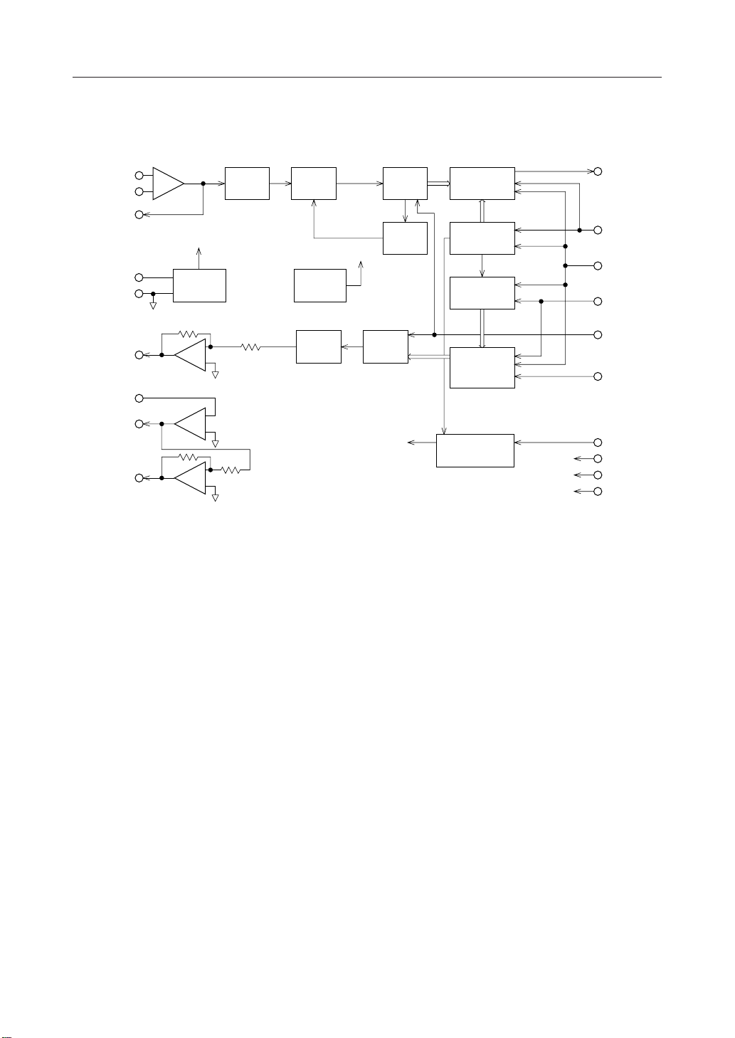
BLOCK DIAGRAM
AIN–
AIN+
GSX
SGC
SG
VFRO
PWI
AOUT–
AOUT+
–
+
SG
GEN
RC
LPF
–
+
–
+
–
+
8th
BPF
GEN
5th
LPF
VR
CONV.
AUTO
ZERO
D/A
CONV.
PWD
A/D
TCONT
PLL
RTIM
RCONT
PWD
Logic
PCMOUT
XSYNC
BCLK
RSYNC
(ALAW)
PCMIN
PDN
V
DD
AG
DG
2/19
¡ Semiconductor ML7000-01/02/03/ML7001-01/02/03
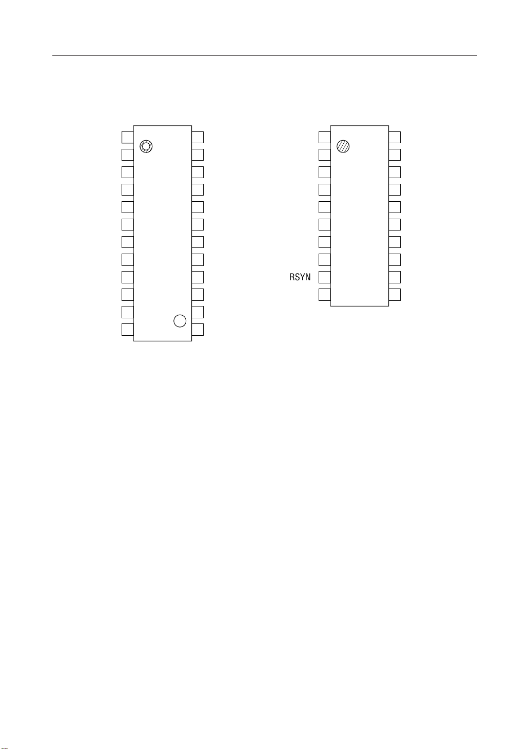
PIN CONFIGURATION (TOP VIEW)
1
SG
AOUT+
AOUT–
RSYNC
PCMIN
2
3
4
NC
5
PWI
6
VFRO
7
NC
8
V
DD
9
DG
10
PDN
11
12 13
24-Pin Plastic SOP
24
23
22
21
20
19
18
17
16
15
14
SGC
AIN+
AIN–
GSX
NC
NC
(ALAW)*
NC
AG
BCLK
XSYNC
PCMOUT
1
SG
AOUT+
AOUT–
RSYNC
PCMIN
2
3
4
PWI
5
VFRO
V
6
DD
7
DG
8
PDN
9
10 11
20-Pin Plastic SSOP
20
19
18
17
16
15
14
13
12
SGC
AIN+
AIN–
GSX
NC
(ALAW)*
AG
BCLK
XSYNC
PCMOUT
* The ALAW pin is only supported by the ML7000-01MA/ML7000-01MB/ML7001-01MA/
ML7001-01MB.
NC : No connect pin
3/19
¡ Semiconductor ML7000-01/02/03/ML7001-01/02/03
PIN FUNCTIONAL DESCRIPTION
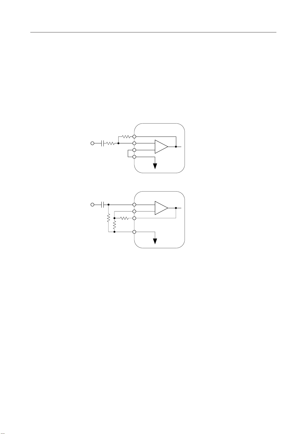
AIN+, AIN–, GSX
Transmit analog input and transmit level adjustment.
AIN+ is a non-inverting input to the op-amp; AIN– is an inverting input to the op-amp; GSX is
connected to the output of the op-amp.
The level adjustment should be performed using any of the methods shown below. During
power-saving and power-down modes, the GSX output is at AG voltage.
Analog input
Analog input
AG
Analog ground.
VFRO
C1
C2
R5
R1
R3
R4
R2
GSX
AIN–
AIN+
SG
AIN+
AIN–
GSX
SG
R1 : variable
–
+
+
–
R2 > 20 kW
C1 > 1/(2 ¥ 3.14 ¥ 30 ¥ R1)
R3 > 20 kW
R4 > 20 kW
R5 > 50 kW
C2 > 1/ (2 ¥ 3.14 ¥ 30 ¥ R5)
Receive filter output.
The output signal has an amplitude of 2.4 VPP for ML7000-xx and 2.0 VPP for ML7001-xx above
and below the signal ground voltage (SG) when the digital signal of +3 dBm0 is input to PCMIN
and can drive a load of 20 kW or more.
For driving a load of less than 20 kW, connect a resistor of 20 kW or more between the pins VFRO
and PWI.
During power-saving or power-down mode, the VFRO output is at an SG level.
When adjusting the receive signal on the basis of frequency characteristics, refer to the Frequency
Characteristics Adjustment Circuit.
4/19
¡ Semiconductor ML7000-01/02/03/ML7001-01/02/03
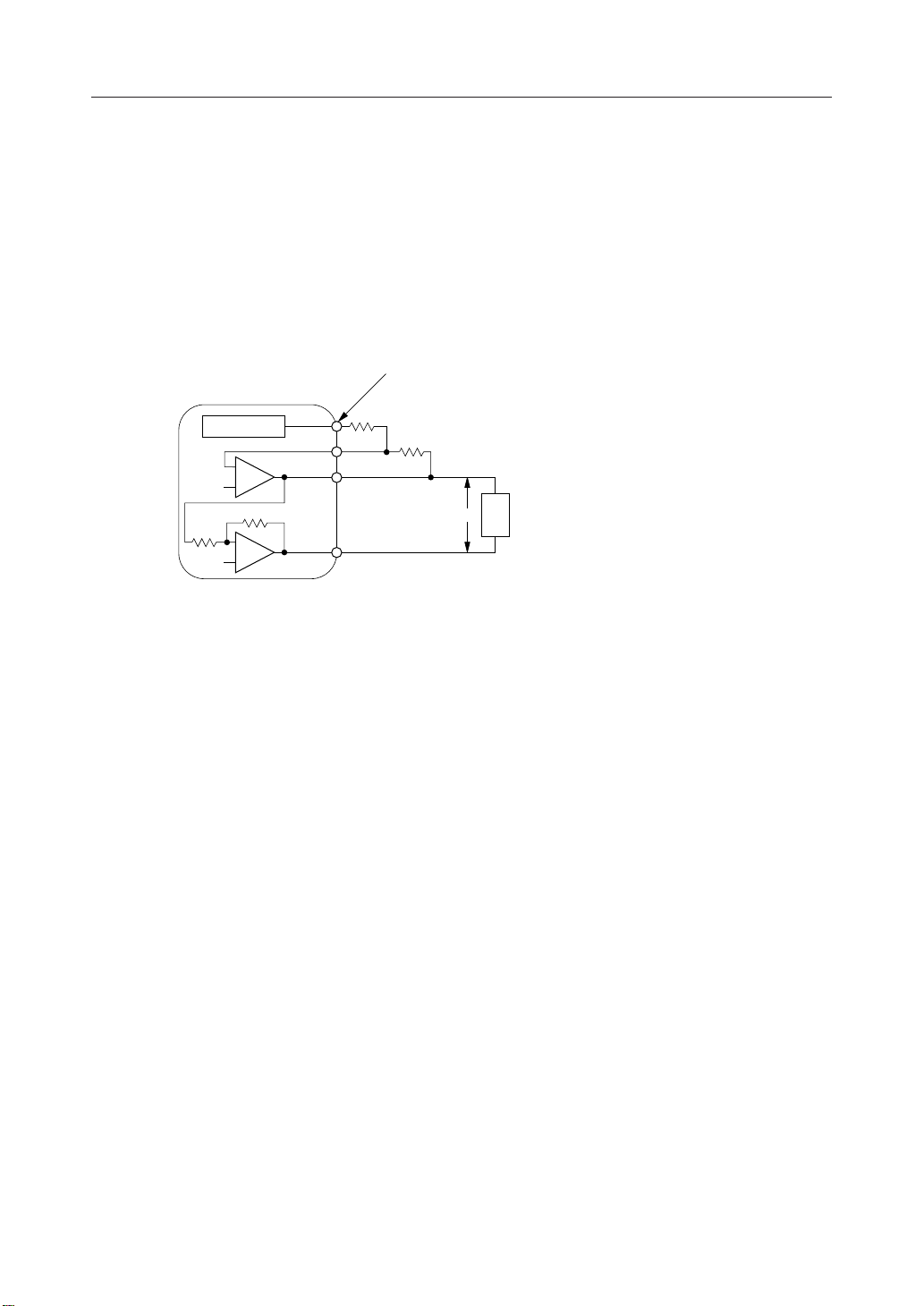
PWI, AOUT+, AOUT–
PWI is connected to the inverting input of the receive driver.
The receive driver output is connected to the AOUT– pin. Therefore, the receive level can be
adjusted with the pins VFRO, PWI, and AOUT–. During power-saving or power down-mode,
the outputs of AOUT+ and AOUT– are in a high impedance state. The output of AOUT+ is
inverted with respect to the output of AOUT–. Since these outputs provide differential drive of
an impedance of 1.2 kW, they can directly be connected to a handset using a piezoelectric
earphone or a line transformer. Refer to the application example.
VI
PWI
R6
R7
VO
ZL
Receive filter
–
+
SG
20 kW
–
+
SG
V
DD
VFRO
AOUT–
20 kW
AOUT+
R6 > 20 kW
ZL > 1.2 kW
Gain = VO/VI = 2 5 R7/R6 £ 2
Power supply for +5 V (ML7000-xx) or +3 V (ML7001-xx)
PCMIN
PCM data input.
A serial PCM data input to this pin is converted to an analog signal in synchronization with the
RSYNC signal and BCLK signal.
The data rate of PCM is equal to the frequency of the BCLK signal.
PCM signal is shifted in at the falling edge of the BCLK signal and latched into the internal
register when shifted by eight bits.
The start of the PCM data (MSD) is identified at the rising edge of RSYNC.
BCLK
Shift clock signal input for the PCMIN and PCMOUT signals.
The frequency, equal to the data rate, is 64, 96, 128, 192, 256, 384, 512, 768, 1024, 1536, 1544, or 2048
kHz. Setting this signal to logic "1" or "0" drives both transmit and receive circuits to the power
saving state.
5/19

¡ Semiconductor ML7000-01/02/03/ML7001-01/02/03
RSYNC
Receive synchronizing signal input.
Eight required bits are selected from serial PCM signals on the PCMIN pin by the receive
synchronizing signal.
Signals in the receive section are synchronized by this synchronizing signal. This signal must be
synchronized in phase with the BCLK. The frequency should be 8 kHz ±50 ppm to guarantee the
AC characteristics which are mainly the frequency characteristics of the receive section.
However, if the frequency characteristic of an applied system is not specified exactly, this device
can operate in the range of 6 to 9 kHz, but the electrical characteristics in this specification are not
guaranteed.
XSYNC
Transmit synchronizing signal input.
The PCM output signal from the PCMOUT pin is output in synchronization with this signal. This
synchronizing signal triggers the PLL and synchronizes all timing signals of the transmit section.
This synchronizing signal must be synchronized in phase with BCLK.
The frequency should be 8 kHz ±50 ppm to guarantee the AC characteristics which are mainly
the frequency characteristics of the transmit section. However, if the frequency characteristic of
an applied system is not specified exactly, this device operates in the range of 6 to 9 kHz, but the
electrical characteristics in this specification are not guaranteed.
Setting this signal to logic "1" or "0" drives both transmit and receive circuits to the power saving
state.
6/19
 Loading...