

OKI ML66Q515-RB, ML66Q517-GA, ML66514-RB, ML66517-GA Datasheet
PEDL66517-03
1
Semiconductor
This version: Nov. 1999
Previous version: Aug. 1999
ML66517 Family
Preliminary
16-Bit Microcontroller
1/28
GENERAL DESCRIPTION
The ML66517 family of highly function al CMOS 16-bit single chip m icrocontrollers utilizes the nX-8/500S, Ok i's
proprietary CPU core.
Each device includes capture input with an internal digital filter, 10-bit A/D converter, a number of timers, and
dedicated 3-phase PWM (6 outputs) function capable of generating and controlling of AC/DC motor driving
waveforms.
By means of the internal dedicated function for motor control, this general-purpose microcontroller is optimally
suited for DC and AC motor control applications for energy saving. And the internal hardware multiplier allows
high-speed arithmetic operations to be executed. And also the internal clock multiplication circuit can reduce the
source frequency noise so that high-speed operations can be performed.
The flash ROM versions (ML66Q517 and ML66Q515) programmable with a single 5V power supply are also
included in the family. These versions are easily adaptable to quick specification changes and to new product
versions.
APPLICATIONS
Air conditioner or inverter control
Motor control for FA equipment
ORDERING INFORMATION
Order Code or Product Name Package Remark
ML66514-RB 5 V mask ROM version
ML66Q515-RB
80-pin plastic QFP
(QFP 80-P-1420-0.80-BK)
5 V flash ROM version
ML66517-GA 5 V mask ROM version
ML66Q517-GA
64-pin plastic SDIP
(SDIP 64-P-750-1.778)
MSM66517 flash ROM version

PEDL66517-03
1
Semiconductor
ML66517 Family
2/28
FEATURES
Name ML66514 ML66517
Operating temperature –40°C to 85°C
Power supply voltage/
Maximum frequency
V
DD
= 4.5 to 5.5 V/f = 25 MHz
Minimum instruction
execution time
80 nsec @25 MHz
Internal ROM size
(max. external)
32 KB (64 KB) 64 KB (128 KB)
Internal RAM size
(max. external)
1 KB (64 KB) 2 KB (64 KB)
I/O ports
46 I/O pins (with pull-up resistors,
programmable at the bit level),
4 input pins
56 I/O pins (with pull-up resistors,
programmable at the bit level),
8 input pins
16-bit free-running counter × 1ch
Compare output/capture input × 2ch
16-bit timer (auto-reload/timer out) × 1ch
8-bit auto reload timer × 2ch
8-bit auto reload timer × 4ch (can
also be used as 16-bit auto reload
timer × 1ch and 8-bit auto reload
timer × 2ch)
Capture × 2ch
8-bit auto reload timer × 2ch
(also functions as serial communication baud rate generators)
8-bit auto reload timer × 1ch (also functions as a watchdog timer)
Timers
8-bit PWM × 2ch (can also be used as
16-bit PWM × 1ch)
8-bit PWM × 4ch (can al so b e used
as 16-bit PWM × 2ch)
Serial port Synchronous/UART × 2ch
A/D converter 10-bit × 4ch 10-bit × 8ch
3-phase PWM (AC motor control) Available
3-phase PWM (DC motor control) Available
External interrupt Non-Maskable × 1ch
Maskable × 2ch
Non-Maskable × 1ch
Maskable × 4ch
Interrupt priority 3 levels
Multiplexed address and data buses
Others
Multiplication calculator
Flash ROM version
ML66Q515
(ROM = 64 KB, RAM = 2 KB)
ML66Q517

PEDL66517-03
1
Semiconductor
ML66517 Family
3/28
SPECIAL FEATURES
1. High-performance CPU
The family includes the high-performance CPU, powerful bit manipulation instruction set, full symmetrical
addressing mode, and ROM WINDOW function, and also provides the best optimized C compiler support.
2. 3-phase PWM circuit for generating motor drive waveforms
The device includes a 16-bit three-phase PWM (six outputs) circuit designed specifically for generating AC
three-phase motor or DC three-phase brushless motor drive waveforms. PWM and level outputs can be switched
by compare and match circuitry and software, and the compare and match circuitry can switch the outputs in real
time.
The device has circuitry to fix the three-phase outputs at an inactive level by inputting malfunction signals from a
motor at the specific pin.
3. Capture inputs with digital filter f ilt ers
The device has two channels of capt ure inputs with 3/4 digital filters. T he device is best suited to event inter val
measurement, pulse width measurement, etc. in a high noise environment such as motor control. An optimum
filter can be selected according to noise width since a sampling interval of an input signal can be selected. A digital
filter OFF mode can also be selected.
4. High-speed multiplier
The device includes a dedicated high-speed multiplier.
The calculation time, 16 bits × 16 bits = 32 bits, is 200 ns (f = 25 MHz).
5. Clock multiplication circuit
The device includes a clock multiplication circuit in which the clock can be selected as a source clock (PLL OFF),
1 × clock, 2 × clock, or 4 × clock.
Therefore, the use of a low frequency oscillator (external clock) allows the device to internally operate at a high
speed, which achieves noise reduction and lower power consumption.
6. Flash memory version programmable wit h a single power supply
In addition to the mask ROM versions, the family includes the vers ions (ML 66Q517 and ML 66Q515) w ith 64 KB
flash memory that can be programmed with a single 5 V supply.
7. A high-precision A/D converter
The device has a high precision 10-bit A/D converter with eight channels.
An independent result register for each channel provides easy accessibility by software.
The A/D converter is activated in a channel select mode, and automatic conversion is also implemented in a scan
mode which sc ans from any designated channel to the last channel (ch 7).
8. Programmable pull-up resistors
Building the pull-up resistors into the chip contributes to overall design compactness. Making them
programmable on a per-bit basis allows co mplete flexibility in circuit board layout and system design. T hese
programmable pull-up resistors are available for all I/O pins not already assigned specific functions (such as the
oscillator connection pins).
PEDL66517-03
1
Semiconductor
ML66517 Family
4/28
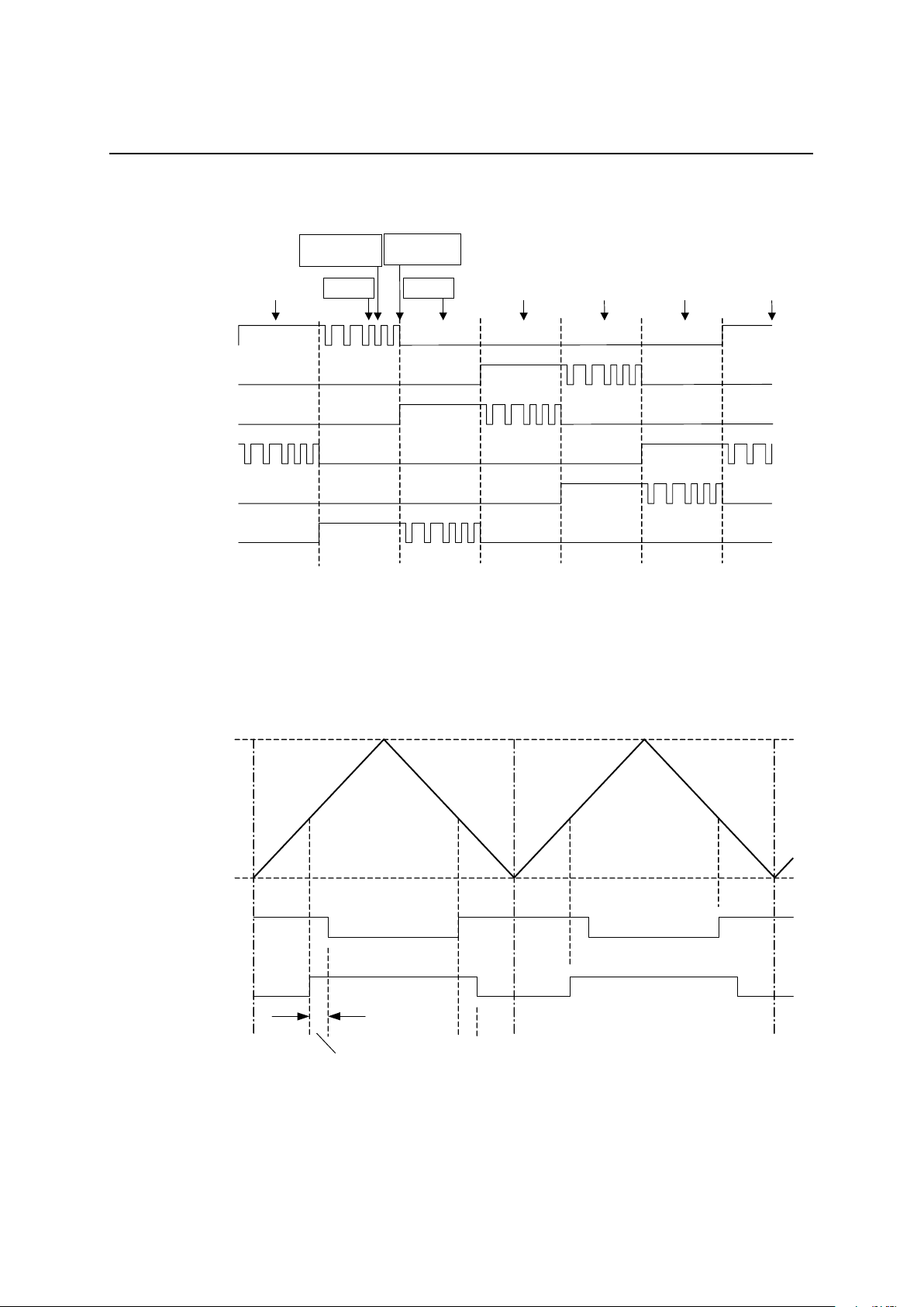
PWM output switching every 60°°°° of motor turn using the compare-out timer
PWM Output Timing (DC Motor Control)
PWM Output Timing (AC Motor Control)
PWM-U
PWM-UB
PWM-V
PWM-VB
PWM-W
PWM-WB
CAP input
Compare regist er
value setting
Compare-match
generation
CAP input
Period register
setting value
16-bit counter value
0000H
PWM-U
(U)
PWM-UB
(U)
Underflow counts up the counter
Set by 8-bit dead-time timer
(Only U and U output signals are indicated above)
PEDL66517-03
1
Semiconductor
ML66517 Family
5/28
BLOCK DIAGRAM
16-bit Timer0
ALU
Memory Control
Pointing Registers
Local Registers
Instruction
Decoder
RAM 2K
8-bit Timer6/WDT
Bus Port Control
System
Control
CPU Core
TM0OUT
TM0EVT
RES
CLKSEL1
CLKSEL0
OSC1
OSC0
EA
PSEN
WR
RD
ALE
3-phase
PWM
INACT
PWMVB
CAP
ROM
64K
A8 to A16
AD0 to AD7
Port Control
P0
P1
P2
P3
P5
P6
P7
P8
P10
P11
P12
TBC
SSP
Control
Registers
LRB
PSW
PC
CSRTSR
ALU Control
ACC
10-bit A/D
Converter
V
REF
AGND
AI0 to AI7
Interrupt
NMI
EXINT0
EXINT3
to
P15
P16
P17
Peripheral
8-bit Timer9
8-bit Timer4/BRG
8-bit Timer3/BRG
TM5EVT
8-bit Timer5
CLKOUT
TM1OUT
TM1EVT
TM2EVT
SIO6
(UART/SYNC)
RXD6
TXD6
RXC6
SIO1
(UART/SYNC)
RXD1
RXC1
TXC1
TXD1
8-bit PWM0
PWM0OUT
PWM2OUT
PWM1OUT
PWM3OUT
8-bit PWM1
8-bit Timer1
8-bit Timer2
TM2OUT
TXC6
PWMV
PWMW
PWMWB
PWMUB
PWMU
CAP/CMP
16-bit FRC
CMP
CAPF0
CAPF1
CPCMF0
CPCMF1
ML66517/ML66Q517 Block Diagram
PEDL66517-03
1
Semiconductor
ML66517 Family
6/28
16-bit Timer0
ALU
Memory Control
Pointing Registers
Local Registers
Instruction
Decoder
RAM
1K/2K
8-bit Timer6/WDT
Bus Port Control
System
Control
CPU Core
TM0OUT
TM0EVT
RES
CLKSEL1
CLKSEL0
OSC1
OSC0
EA
PSEN
WR
RD
ALE
ROM
32K/64K
A8 to A15
AD0 to AD7
Port Control
P0
P1
P3
P5
P6
P7
P8
P11
P12
TBC
SSP
Control
Registers
LRB
PSW
PC
ALU Control
ACC
P15
P16
P17
3-phase
PWM
INACT
PWMVB
CAP
10-bit A/D
Converter
V
AGND
AI4 to AI7
Interrupt
NMI
EXINT0
EXINT1
REF
to
Peripheral
8-bit Timer9
8-bit Timer4/BRG
8-bit Timer3/BRG
8-bit Timer5
CLKOUT
SIO6
(UART/SYNC)
RXD6
TXD6
RXC6
SIO1
(UART/SYNC)
RXD1
RXC1
TXC1
TXD1
8-bit PWM0
PWM0OUT
PWM1OUT
8-bit PWM1
TXC6
PWMV
PWMW
PWMWB
PWMUB
PWMU
CAP/CMP
16-bit FRC
CMP
CAPF0
CAPF1
CPCMF0
CPCMF1
*1
*2
*1 ML66Q515 has 2KB RAM, ML66514 has 1KB RAM
*2 ML66Q515 has 64KB ROM, ML66514 has 32KB ROM
ML66Q515/ML66514 Block Diagram
PEDL66517-03
1
Semiconductor
ML66517 Family
7/28
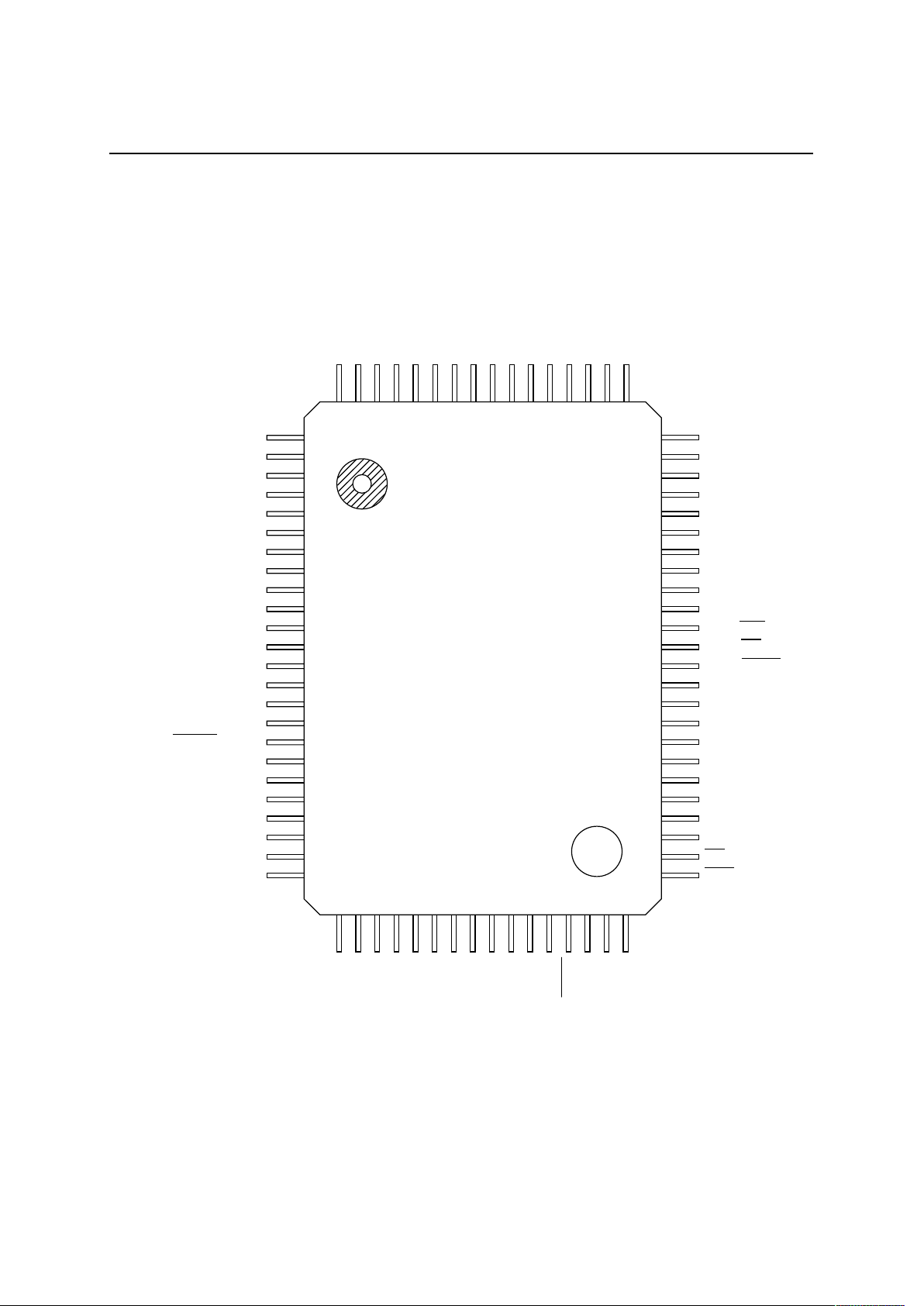
PIN CONFIGURATION (TOP VIEW)
TXC1/P8-3
PWM2OUT/P8-6
PWM3OUT/P8-7
PWM0OUT/P7-6
PWM1OUT/P7-7
V
DD
GND
PWMU/P16-0
PWMUB/P16-1
PWMV/P16-2
PWMVB/P16-3
PWMW/P16-4
PWMWB/P16-5
INACT/P16-6
NMI
CAPF0/P17-0
CAPF1/P17-1
CPCMF0/P17-2
CPCMF1/P17-3
EXINT0/P6-0
EXINT1/P6-1
P1-6/A14
P1-5/A13
P1-4/A12
P1-3/A11
P1-2/A10
P1-1/A9
P1-0/A8
GND
P3-3/WR
P3-2/RD
P3-1/PSEN
P3-0/ALE
P0-7/AD7
P0-6/AD6
P0-5/AD5
P0-4/AD4
P0-3/AD3
P0-2/AD2
P0-1/AD1
P0-0/AD0
EA
RES
CLKSEL1
CLKSEL0
V
DD
OSC1
OSC0
GND
P11-2/CLKOUT
P10-7/TM5EVT
P5-7/TM0EVT
P5-6/TM0OUT
P6-7/TM2OUT
P6-6/TM2EVT
P6-5/TM1OUT
P6-4/TM1EVT
P6-3/EXINT3
P6-2/EXINT2
V
DD
V
REF
AI0/P12-0
AI1/P12-1
AI2/P12-2
AI3/P12-3
AI4/P12-4
AI5/P12-5
AI6/P12-6
AI7/P12-7
AGND
GND
RXD6/P15-0
TXD6/P15-1
RXC6/P15-2
TXC6/P15-3
RXD1/P8-0
TXD1/P8-1
RXC1/P8-2
65707580
1
5
10
15
20
60
55
50
45
40353025
P1-7/A15
P2-0/A16
80-Pin Plastic QFP
ML66517/ML66Q517 Pin Config ur atio n
PEDL66517-03
1
Semiconductor
ML66517 Family
8/28
TXC1/P8-3
PWM0OUT/P7-6
PWM1OUT/P7-7
PWMU/P16-0
PWMUB/P16-1
PWMV/P16-2
PWMVB/P16-3
PWMW/P16-4
PWMWB/P16-5
INACT/P16-6
NMI
CAPF0/P17-0
CAPF1/P17-1
P1-3/A11
P1-2/A10
P1-1/A9
P1-0/A8
GND
P3-3/WR
P3-2/RD
P3-1/PSEN
P3-0/ALE
P0-7/AD7
P0-6/AD6
P0-5/AD5
P0-4/AD4
P0-3/AD3
P0-2/AD2
P0-1/AD1
P0-0/AD0
EA
RES
CLKSEL1
CLKSEL0
V
DD
OSC1
OSC0
GND
P11-2/CLKOUT
P5-7/TM0EVT
P5-6/TM0OUT
P6-1/EXINT1
P6-0/EXINT0
P17-3/CPCMF1
P17-2/CPCMF0
A12/P1-4
A13/P1-5
A14/P1-6
A15/P1-7
V
DD
V
REF
AI4/P12-4
AI5/P12-5
AI6/P12-6
AI7/P12-7
AGND
GND
RXD6/P15-0
TXD6/P15-1
RXC6/P15-2
TXC6/P15-3
RXD1/P8-0
TXD1/P8-1
RXC1/P8-2
496064
1
10
48
40
33
17 30
64-Pin Plastic QFP
ML66Q515/ML66514 Pin Config ur atio n

PEDL66517-03
1
Semiconductor
ML66517 Family
9/28
PSEN/P3-1
P3-0/ALE
P0-7/AD7
P0-6/AD6
P0-5/AD5
P0-4/AD4
P0-3/AD3
P0-2/AD2
P0-1/AD1
P0-0/AD0
EA
RES
CLKSEL1
CLKSEL0
V
DD
OSC1
OSC0
GND
P11-2/CLKOUT
P5-7/TM0EVT
P5-6/TM0OUT
P6-1/EXINT1
P6-0/EXINT0
P17-3/CPCMF1
P17-2/CPCMF0
P17-1/CAPF1
P17-0/CAPF0
NMI
P16-6/INACT
P16-5/PWMWB
P16-4/PWMW
P16-3/PWMVB
P16-2/PWMV
RD/P3-2
WR/P3-3
GND
A8/P1-0
A9/P1-1
A10/P1-2
A11/P1-3
A12/P1-4
A13/P1-5
A14/P1-6
A15/P1-7
V
DD
V
REF
AI4/P12-4
AI5/P12-5
AI6/P12-6
AI7/P12-7
AGND
GND
RXD6/P15-0
TXD6/P15-1
RXC6/P15-2
TXC6/P15-3
RXD1/P8-0
TXD1/P8-1
RXC1/P8-2
TXC1/P8-3
PWM0OUT/P7-6
PWM1OUT/P7-7
PWMU/P16-0
PWMUB/P16-1
64-Pin Plastic SDIP
ML66Q515/ML66514 Pin Config ur atio n
 Loading...