

D
ATA SHEET
O K I
G a A s
P R O D U C T S
10-Gbps GaAs Family
High-Speed Optical Communications System
April 1999

–––––––––––––––––––––––––––––––––––––––––––––––––––––––––––––––––––––––––––––––––––––––––––
■ ■
CONTENTS
10-GHz GaAs Family
.........................................................................................................................1
KGL4201
10-GHz 8:1 Multiplexer ............................................................................................................................. 3
KGL4202
10-GHz 1:8 Demultiplexer ........................................................................................................................ 7
GHDD4411
EX-OR Circuit.......................................................................................................................................... 11
GHDD4414
Decision Circuit with Phase Detector...................................................................................................... 15
Oki Semiconductor
10-GHz GaAs Family
fT (GHz)
Gate Delays
(ps)
Application
High-Speed Optical Communications Systems
INTRODUCTION
Oki’s 10-GHz logic devices are manufactured using a 0.2-µm, ion-implanted process, which is similar to
Oki’s familiar 0.5-µm telecommunications process. However, the 0.2-µm process uses a phase-shifting
edge line (PEL) masking method for gate fabrication. Gold-based, three-level metal interconnections are
used for high density and shorter wiring paths. Layers 1 and 2 are signal lines. Layer 3, which is formed
by electroplating, is used for ground or power supply lines because of its lower resistance. An optional
buried “p” channel structure is adopted for reducing short channel effects.
The following table shows the digital GaAs logic processes of the 10-GHz GaAs family.
GaAs Logic Processes
Basic FET Process
MESFET DCFL or SBFL I-line printing 0.5 30 25 < 2.4 Gbps standard cell
MESFET DCFL or SBFL PEL < 0.2 60 9 >12-Gbps hand-routed logic
Pseudomorphic-inverted HEMT DCFL or SBFL PEL 0.2 > 60 7 > 20-Gbps low-density logic
Pseudomorphic BP--MESFET Analog Deep UV 0.2 > 60 – Analog amplifier
Basic Gate
Circuit
Photo Masking
The key to operating reliably at 10 Gbps is logic circuitry that can easily manipulate data at over 13 Gbps.
The higher frequency overhead is required to meet the different clock skews encountered when designing and routing 10-Gbps data management hardware.
The logic is either direct-coupled FET logic (DCFL) or source-coupled FET logic (SCFL). The low-drive
disadvantage of DCFL can be improved by using super-buffer FET logic (SBFL). The basic speed of SBFL
is slower than DCFL, but SBFL is faster with higher fanouts and longer metal runs. A designer selects the
best performing logic for each logic element application. SBFLs used for clock distribution, output buffers, etc. Typical gate delays of 9 ps and power of 2 mW per gate are achieved. Register logic elements like
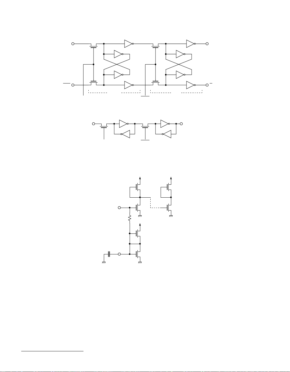
D-flip flops are assembled using memory cell flip flops (MCFF) as shown in Figure 1 .The operation speed
of a MCFF, which is about twice that of a conventional 6 NOR-gate circuit, operates at very low power.
To simplify device interconnections, AC-coupled clock and data input lines are created using the circuit
shown in Figure 2 .
Gate Length
(µm)
FEATURES
• 10-Gbps operation: highest speed available
• ECL level logic swings: easy interface to other
logic
• Inputs internally terminated: reduces noise and
phase jitter
• 50-Ω I/Os: easy to interconnect hardware
1Oki Semiconductor
10-GHz GaAs Family ■ ––––––––––––––––––––––––––––––––––––––––––––––––––––––––––––––––––––––––––
Data
Data
Master Slave
Clock Clock
Data
Clock Clock
Figure 1. Memory Cell Flip-Flops
Data or Clock In
Master/Slave Flip-Flop
Flip-Flop
Out
Q
■
Q
50Ω
Reference
Dummy Gate
Figure 2. AC-Coupled, Self-Biased Logic Input
Many 10-Gbps inputs are self-biased and 50coupled to drive 50-
Ω
ground terminated lines.
Ω
terminated, for capacitance coupling. The outputs are DC-
DATA SHEETS
This document contains data sheets for the KGL4201, KGL4202, GHDD4411, and GHDD4414 10-Gbps
GaAs High-Speed Optical Communication Systems.
Data sheets for other communication devices may be obtained from the Oki Semiconductor WEB site,
www.okisemi.com or from the local sales office.
2 Oki Semiconductor
KGL4201
10-GHz 8:1 Multiplexer
GENERAL DESCRIPTION
Oki’s KGL4201 is a 10-GHz 8:1 multiplexer designed to operate in 10-Gbps communication links. This
circuit synchronously merges eight 1.25-Gbps data streams, clocked at low frequency rates into a single
10-Gbps stream, clocked at the higher frequency. In the KGL4201 multiplexer, the 10-GHz master clock is
first divided by two, then by four. The lower frequency components are first multiplexed by four, then
the two groups are merged into a single data stream using the master 10-Gbps clock. Complementary
1/8 synchronous clock outputs are made available from the KGL4201 for use in synchronizing lower frequency logic.
All signal interfaces are 50-
1.25-Gbps clock outputs. The 10-Gbps data output and 10-GHz clock input are AC-capacitively-coupled
for ease of interfacing at microwave speeds and reducing ground noise induced phase jitter. All package
clock and data pins are separated by either ground or supply voltage pins to control the I/O impedance,
maintain signal isolation and reduce phase noise.
The KGL4201 is shipped in a 40-pin ceramic flat-package with impedance-controlling ground plane and
flush mounting bottom heat sink.
Ω
with direct DC coupling on the 1.25-Gbps data inputs and phase-locked
FEATURES
• AC-coupled 10 Gbps I/O: eliminates DC
coupled phase jitter
• 1/8 clock generated on chip: easy to
synchronize downstream logic
• 2 V, 2.4 W
• Isolated I/O pins: minimize noise and
impedance variation
• Packaged in 40-pin ceramic flat-package with
ground plane and heat sink.
3Oki Semiconductor
KGL4201 ■ –––––––––––––––––––––––––––––––––––––––––––––––––––––––––––––––––––––––––––––––––––
PIN CONFIGURATION
Pin Configuration
Pin
Name Pin Pin Name Pin Pin Name Pin Pin Name
1
11.43 SQ
10
14.84 SQ
13.01 SQ
10.67 SQ
40
11
1.27
40
1
31
14.84 SQ
20
13.01 SQ
11.0 SQ
30
21
31
30
0.7 ±0.05
0.9 ±.005
1.7 ±0.15
2 ±0.3
0.125 ±0.050.4 ±0.05
1 GND 11 GND 21 VDD 31 GND
2 Q 12 VDD 22 GND 32 VDD
3 GND 13 D0 23 GND 33 D7
4Q
5 GND 15 D2 25 GND 35 D5
6 GND 16 D4 26 GND 36 D3
14 GND 24 CK 34 GND
10
11
1.27
21
20
0.4 ±0.05
7 1/8CK 17 GND 27 RCK 37 GND
8 GND 18 D6 28 GND 38 D1
9 1/8CK
10 VB 20 GND 30 GND 40 VDD
BLOCK DIAGRAM
19 GND 29 GND 39 VB
2 ±0.3
1.7 ±0.15
0.9 ±.005
0.7 ±0.05
■
D0
D2
D4
D6
D1
D3
D5
D7
4 Oki Semiconductor
4:1 MUX
4:1 MUX
1/8CK 1/8CK
1/4 Divider CK
2:1
MUX
1/2
Divider
delay
Output
Latch
delay
Q
Q
––––––––––––––––––––––––––––––––––––––––––––––––––––––––––––––––––––––––––––––––––– ■ KGL4201 ■
ELECTRICAL CHARACTERISTICS
RECOMMENDED OPERATING CONDITIONS
Rated Value
Parameter
Power supply voltage for internal logic V
Power supply voltage for output buffer V
Operating temperature range at package base T
DD
B
S
Symbol
UnitMin Typ Max
1.9 2.0 2.1 V
1.9 2.0 2.1 V
0 – 70 °C
DC CHARACTERISTICS
V
= 2V ±0.1V, VB=2V ±0.1V Ts = 0 to 70°C
DD
Rated Value
Parameter Symbol Test Condition
UnitMin. Typ. Max.
Power dissipation P – 2.4 3.0 W
High-level 1/8 CK output voltage V
Low-level 1/8 CK output voltage V
Data output voltage swing V
Clock input voltage swing V
High-level data input voltage V
Low-level data input voltage V
OH
OL
OD
CK
IDH
IDL
50-
Ω
load 0.7 1.2 V
Capacitive coupling 0.5 0.9 V
0.85 1.3 V
0 0.3 V
P-P
P-P
0.8 1.3 V
0 0.3 V
AC CHARACTERISTICS
VDD = 2V ±0.1V, VB=2V ±0.1V Ts = 0 to 70°C
Rated Value
Parameter Symbol Test Condition
Minimum clock period
Setup time (Data to 1/8 CK ↓)t
Hold time (1/8 CK ↓ to Data) t
CK-D[7:0] phase margin
Rise time (Q, Q
Fall time (Q, Q
)t
)t
∆
t
C
PS
DH
∆
t
M
R
F
– – 100 ps
450 500 550 ps
-400 -350 -300 ps
Input clock period is 100 ps 550 650 ps
20 30 40 ps
20 30 40 ps
UnitMin. Typ. Max.
5Oki Semiconductor
■ KGL4201 ■ –––––––––––––––––––––––––––––––––––––––––––––––––––––––––––––––––––––––––––––––––––
INTERFACE TIMING
CK
D0
D1
D2
D3
D4
D5
D6
D7
Q
Q H1 G1 F1 E1 D1 C1 B1 A1 H2 G2 F2 E2 D2 C2 B2 A2 C3 B3 A3
1/8 CK
1/8 CK
A1 A2 A3 A4
B1 B2 B3 B4
C1 C2 C3 C4
D1 D2 D3 D4
E1 E2 E3 E4
F1 F2 F3 F4
G1 G2 G3 G4
H1 H2 H3 H4
H1G1F1E1D1C1B1A1 H2G2F2E2D2C2B2A2 C3B3A3
6 Oki Semiconductor

KGL4202
10-GHz 1:8 Demultiplexer
GENERAL DESCRIPTION
Oki’s KGL4202 is a 10-GHz 1:8 demultiplexer designed to operate in 10-Gbps communication links. This
circuit synchronously separates a single 10-Gbps data stream, clocked at up to 10 GHz, into eight lower
frequency data streams, clocked at lower frequency rates. In the KGL4202 demultiplexer, the 10-GHz
master clock is first divided by two, then by four. The 10-Gbps data stream is first divided into two synchronous serial paths, then these two data streams are separated into four each lower speed data streams
and brought out to data latched outputs. Complementary 1/8 synchronous clock outputs are made available from the KGL4202 for use in synchronizing lower frequency logic.
All signal interfaces are 50 Ω with all inputs internally terminated in 50 Ω. Direct DC coupling is used on
the 10-Gbps data input, the 1.25-Gbps data outputs and phase-locked 1.25-Gbps clock outputs. The 10GHz clock input is AC-capacitively-coupled for ease of interfacing at microwave speeds and reducing
ground noise induced phase jitter. The package 10-GHz clock and 10-Gbps data pins are separated by
ground pins to control the I/O impedance, maintain signal isolation and reduce phase noise. The eight
data outputs are distributed to opposite sides of the package to facilitate hardware layout and reduce
noise. Over one third of the chip power is due to the ten 50-Ω outputs.
The KGL4202 is shipped in a 40-pin ceramic flat-package with impedance-controlling ground plane and
flush-mounting bottom heat sink.
FEATURES
• AC-coupled 10 Gbps I/O: eliminates DC
coupled phase jitter
• 1/8 clock generated on chip: easy to
synchronize downstream logic
• Isolated I/O pins: minimizes noise and
impedance variation
• 2 V, 3.2 W
• Packaged in 40-pin ceramic flat-package with
ground plane and heat sink
7Oki Semiconductor

■ KGL4202 ■ –––––––––––––––––––––––––––––––––––––––––––––––––––––––––––––––––––––––––––––––––––
PIN CONFIGURATION
1
11.43 SQ
10
14.84 SQ
13.01 SQ
10.67 SQ
40
11
1.27
31
30
21
20
0.7 ±0.05
0.9 ±.005
1.7 ±0.15
2 ±0.3
0.125 ±0.050.4 ±0.05
Pin Configuration
Pin Name Pin Pin Name Pin Pin Name Pin Pin Name
1 GND 11 GND 21 VDD 31 GND
2 1/8CK
3 GND 13 Q1 23 GND 33 Q6
4 1/8CK 14 GND 24 CKIN 34 GND
5 RD 15 Q3 25 GND 35 Q4
6 GND 16 Q5 26 GND 36 Q2
7 N.C. 17 GND 27 RCK 37 GND
8 GND 18 Q7 28 GND 38 Q0
9 GND 19 VB 29 GND 39 VB
10 VB 20 GND 30 VB 40 VDD
12 VDD 22 GND 32 VDD
BLOCK DIAGRAM
8 Oki Semiconductor
Q0
D
CK
1:2
DEMUX
delay
1/2 Divider 1/4 Divider
1:4 DEMUX
1:4 DEMUX
1/8CK 1/8CK
Q2
Q4
Q6
Q1
Q3
Q5
Q7
1/8CK
1/8CK

––––––––––––––––––––––––––––––––––––––––––––––––––––––––––––––––––––––––––––––––––– ■ KGL4202 ■
ELECTRICAL CHARACTERISTICS
ABSOLUTE MAXIMUM RATINGS
Rated Value
Parameter Symbol
Supply voltage for internal logic V
Supply voltage for output buffer V
DD
B
-0.3 2.3 V
-0.3 2.3 V
UnitMin. Max.
Clock input CK -0.3 1.5 V
Data inputs D -0.3 1.5 V
Temperature at package base under bias T
Storage temperature T
S
ST
-45 100 °C
-45 125 °C
RECOMMENDED OPERATING CONDITIONS
Rated Value
Parameter Symbol
Power supply voltage for internal logic V
Power supply voltage for output buffer V
Operating temperature range at package base T
DD
B
S
1.9 2.0 2.1 V
1.9 2.0 2.1 V
0 – 70 °C
UnitMin. Typ. Max.
DC CHARACTERISTICS
VDD = 2 V ±0.1 V, VB=2 V ±0.1 V TS = 0 to 70°C
Rated Value
Parameter Symbol Test Condition
Power dissipation P 3.2 4.0 W
High-level 1/8CK output voltage V
Low-level 1/8CK output voltage V
Data input voltage swing V
Clock input voltage swing V
OH
OL
ID
ICK
50-Ω load 0.85 1.3 V
50-Ω load 0 0.3 V
Capacitive coupling 0.5 0.9 V
Capacitive coupling 0.5 0.9 V
AC CHARACTERISTICS
VDD = 2V ±0.1V, VB=2V ±0.1V Ts = 0 to 70°C
Rated Value
Parameter Symbol Test Condition
Minimum clock period ∆t
Setup time (D to CK ↓)t
Hold time (CK ↓ to D) t
CK-D phase margin ∆t
1/8CK ↑ to valid data delay t
DS
DH
C8Q
C
M
Input clock period is 100 ps 50 65 ps
-55 -45 -35 ps
70 80 90 ps
-40 -10 20 ps
100 ps
UnitMin. Typ. Max.
P-P
P-P
UnitMin. Typ. Max.
9Oki Semiconductor

■ KGL4202 ■ –––––––––––––––––––––––––––––––––––––––––––––––––––––––––––––––––––––––––––––––––––
INTERF ACE TIMING
CK
D
Q0
Q1
Q2
Q3
Q4
Q5
Q6
Q7
1/8 CK
1/8 CK
TIMING
CK
D
H1G1F1E1D1C1B1A1 H2G2F2E2D2C2B2A2
A1 A2 A3
B1 B2 B3
C1 C2 C3
D1 D2 D3
E1 E2 E3
F1 F2 F3
G1 G2 G3
H1 H2 H3
∆t
C
∆t
t
t
DH
DS
M
H3G3F3E3D3C3B3A3 D4C4B4A4
1/8 CK
1/8 CK
t
C8Q
Q[7:0] Valid Valid
10 Oki Semiconductor

GHDD4411
EX-OR Circuit
GENERAL DESCRIPTION
Oki’s GHDD4411 is a 10-GHz exclusive-OR/NOR circuit designed to function in 10-Gbps high-speed
communication serial bit streams. The EX-OR must operate from both rising and falling edges at an
equivalent speed of 20-Gbps non-return-to-zero (NRZ) signal to extract a 10-Gbps clock from a 10-Gbps
signal. Using closely matched Gilbert cell circuitry, this device operates at over 10 Gbps using DCFL and
SBFL logic from inverted HEMT technology. Internal input 50-Ω terminations and a self-referencing bias
voltage allow capacitive coupling, simplifying interconnections.
The GHDD4411 EX-OR circuit is high-speed in a 28-pin ceramic flat package with impedance-controlling
ground plane and flush-mounting bottom heat sink.
FEATURES
• EX-OR and EX-NOR: outputs optimized for
performance
• 1.5 V, 0.6 W: lowest power with 50-Ω interfaces
• Packaged in 28-pin ceramic flat package with
ground plane and heat sink
11Oki Semiconductor

■ GHDD4411 ■ ––––––––––––––––––––––––––––––––––––––––––––––––––––––––––––––––––––––––––––––––––
PIN CONFIGURATION
6 ±0.1
11
0.125
12 ±0.1
2
2
16 ±0.1
12
9.6 0.5
8
1
7
9
8.6
5
1.27
10.16
15
2028
146
0.3
2.1 ±0.1
0.5
0.5
19
15
Dimensions in mm
Pin Signal Function Pin Signal Function
1 IN1BS Input 1 bias input 15 VB Power supply (buffer)
2 N.C. No Connect 16 N.C. No Connect
3 IN1RF Input 1 bias reference output 17 IN2RF Input 2 bias reference output
4 N.C. No Connect 18 N.C. No Connect
5 VB Power supply (buffer) 19 IN2BS Input 2 bias input
6 GND Ground 20 GND Ground
7 EXOR EX-OR output 21 IN2 Data input 2
8 GND Ground 22 GND Ground
9 N.C. No Connect 23 VD Power supply (logic circuit)
10 N.C. No Connect 24 N.C. No Connect
11 N.C. No Connect 25 VD Power supply (logic circuit)
12 GND Ground 26 GND Ground
13 EXNOR EX-NOR output 27 IN1 Data input 1
14 GND Ground 28 GND Ground
12 Oki Semiconductor

––––––––––––––––––––––––––––––––––––––––––––––––––––––––––––––––––––––––––––––––– ■ GHDD4411 ■
BLOCK DIAGRAM
IN1
RF
IN1
IN2
IN2
IN1
IN2
EXNOR
BS
BS
RF
EXOR
13Oki Semiconductor

■ GHDD4411 ■ ––––––––––––––––––––––––––––––––––––––––––––––––––––––––––––––––––––––––––––––––––
ELECTRICAL CHARACTERISTICS
Absolute Maximum Ratings
Parameter Symbol Min Max Unit
Suuply voltage for internal logic V
Supply voltage for outpu buffer V
DD
B
Clock input CK -0.3 1.0 V
Data input D -0.3 1.0 V
Temperature at package base under bias T
Storage temperature T
S
ST
Recommended Operating Conditions
Parameter Symbol Min. Typ. Max. Unit
Suuply voltage for internal logic V
Supply voltage for output buffer V
Operating temperature range at package base T
V
= 1.5 V ±0.1, VB = 1.5 V ± 0.1, TS = 0 to 70 °C
DD
Parameter Symbol Condition Min. Typ. Max. Unit
Power dissipation P 0.6 W
Input bit rate B 10 Gb/s
Data input voltage amplitude V
Data output voltage amplitude V
Data output rise/fall time τ 20 ps
DD
B
S
ID
OD
Capacitive coupling 0.2 0.8 V
50-Ω load,
Capacitive coupling
-0.3 2.3 V
-0.3 2.3 V
-45 100 °C
-45 125 °C
1.4 1.5 1.6 V
1.4 1.5 1.6 V
070°C
P-P
0.7 V
P-P
OUTPUT WAVEFORM
14 Oki Semiconductor
I63A-7, DEC12,5-7, 25C, P
Horizontal - 20ps/Div, Vertical - 200 mV/div

GHDD4414
Decision Circuit with Phase Detectors
GENERAL DESCRIPTION
Oki’s GHDD4414 is a 10-GHz decision circuit designed to strip data from high-speed serial bit streams in
10-Gbps communication links. Using a clock input at up to 10 GHz and using D-flip-flops, EX-ORs, and
phase detectors, this circuit separates a 10-Gbps data stream into: clock output, data output, “phase”
variation output, and data density output.
A 10-GHz master clock drives two D-flip-flops in this circuit. Buffered input data is clocked through the
first flip-flop, then the second, “data out” is taken from the first flip-flop. The data input buffer is composed of a series of inverters to delay the signal and obtain a small decision ambiguity. A phase comparison is made of the buffered data and data from flip-flop one; a second phase comparison is made of the
output of flip-flops one and two. The phase detectors are modified EX-OR circuits with resistor summing
of the logic gates to permit analog measurement of their outputs. Any change in the timing relationships
between the clock and data is seen at the output of the first phase detector. The second flip-flop operates
as a 1-bit shift register with fixed 360-deg phase shift. The second phase detector output depends only
upon the transition density (speed of rise and fall transitions) of the input data signal.
All signal interfaces are 50-Ω with all inputs internally terminated in 50 Ω. The 10-GHz clock and data
inputs are AC capacitively-coupled for ease of interfacing at microwave speeds and reducing ground
noise induced phase jitter. Data and phase outputs are DC-coupled.
FEATURES
• Phase detectors on chip: verifies data integrity
• Isolated 10-Gbps input pins: minimizes noise
and impedance variation
• 1.5 V, 1 W: lowest power with 50-Ω interfaces
• 28-pin ceramic flat package with impedance
controlling ground plane and flush mount heat
sink
15Oki Semiconductor

■ GHDD4414 ■ ––––––––––––––––––––––––––––––––––––––––––––––––––––––––––––––––––––––––––––––––––
PIN CONFIGURATION
6 ±0.1
11
0.125
12 ±0.1
2
2
16 ±0.1
12
9.6 0.5
8
1
7
9
8.6
5
1.27
10.16
15
2028
146
0.3
2.1 ±0.1
0.5
0.5
19
15
Dimensions in mm
Pin Signal Function Pin Signal Function
1C
BS
Clock bias input 15 V
B
Power supply (buffer)
2 NC 16 P1 Phase detector output
3C
MB
Clock output duty monitor 17 P2 Phase detector ref. output 1
4 NC 18 P3 Phase detector ref. output 2
5V
B
Powr supply (buffer) 19 V
D
Power supply (logic circuit)
6 GND 20 GND
7D
OUT
Data output 21 D
IN
Data input
8 GND 22 GND
9NC 23D
10 NC 24 D
11 NC 25 V
BS
RF
D
Data bias input
Data bias reference output
Power supply (logic circuit)
12 GND 26 GND
13 C
OUT
Clock output 27 CK Clock input
14 GND 28 GND
16 Oki Semiconductor

––––––––––––––––––––––––––––––––––––––––––––––––––––––––––––––––––––––––––––––––– ■ GHDD4414 ■
BLOCK DIAGRAM
D
OUT
Phase Detector
PD
P
1
D
D
BS
D
RF
CK
C
BS
D Q
APPLICATION BLOCK DIAGRAM
Fiber Input
Pin-PD &
PreAmp
AGC Amp
Delay
D Q
Rectifier Filter
PD
PD
Phase
Shifter
LPF C
Limiting
Amp
P
2
P
3
MB
C
OUT
Decision
Circuit
Clock
Out
17Oki Semiconductor

■ GHDD4414 ■ ––––––––––––––––––––––––––––––––––––––––––––––––––––––––––––––––––––––––––––––––––
ELECTRICAL CHARACTERISTICS
VDD = 1.5 V ±0.1 V, VB = 1.5 V ±0.1 V, TS = 0° to 70°C
Parameter Symbol Condition Min. Max. Unit
Power dissipation P 1 W
Decision ambiguity V
IDEC
Phase margin ∆ θ 250 degree
Data input voltage amplitude V
Clock input voltage amplitude V
Data output voltage amplitude V
Clock output voltage amplitude V
Clock output duty cycle D
Clock to data delay τ
ID
IC
OD
OC
TYC
25 45 ps
CD
Phase detection sensitivity ∆ V θ 10 Gbps
10 Gbps
15
-1
PRBS: 2
Capacitive coupling 0.8 V
0.4 0.8 V
50Ω load
capacitive coupling
0.7 V
0.7 V
40 60 %
PRBS: 2
15
-1
0.28 mV/degree
0.05 V
P-P
P-P
P-P
P-P
P-P
Phase Detection Characteristics (DIN Amplitude = 0.7-V
P-P
)
CIN Delay (ps) P1 (V) P2 (V) P3 (V) Comments
+29 0.350 0.343 0.443 Maximum delay for ER <10
-10
0 0.383 0.340 0.443 Center of phase margin
-29 0.424 0.342 0.443 Minimum delay for ER <10
-10
PHASE DETECTOR CIRCUIT
Input 1
Output
Input 2
18 Oki Semiconductor

––––––––––––––––––––––––––––––––––––––––––––––––––––––––––––––––––––––––––––––––– ■ GHDD4414 ■
PHASE DETECTION BETWEEN SIGNAL AND CLOCK AT 10 Gbps
400
P1[mV]
P2[mV]
350
300
250
Output Voltage of PD (mV)
P3[mV]
TIMING
200
Error Free Range
-270 -180 -90 0 90 180 270
Phase Variation (degree)
Data
Clock
200mV/div
25ps/div
19Oki Semiconductor

■ GHDD4414 ■ ––––––––––––––––––––––––––––––––––––––––––––––––––––––––––––––––––––––––––––––––––
20 Oki Semiconductor

The information contained herein can change without notice owing to product and/or technical improvements.
Please make sure before using the product that the information you are referring to is up-to-date.
The outline of action and examples of application circuits described herein have been chosen as an explanation of the standard action
and performance of the product. When you actually plan to use the product, please ensure that the outside conditions are reflected in
the actual circuit and assembly designs.
Oki assumes no responsibility or liability whatsoever for any failure or unusual or unexpected operation resulting from misuse, neglect,
improper installation, repair, alteration or accident, improper handling, or unusual physical or electrical stress including, but not limited
to, exposure to parameters outside the specified maximum ratings or operation outside the specified operating range.
Neither indemnity against nor license of a third party's industrial and intellectual property right,etc.is granted by us in connection with
the use of product and/or the information and drawings contained herein. No responsibility is assumed by us for any infringement of a
third party's right which may result from the use thereof.
When designing your product, please use our product below the specified maximum ratings and within the specified operating ranges,
including but not limited to operating voltage, power dissipation, and operating temperature.
The products listed in this document are intended for use in general electronics equipment for commercial applications (e.g.,office
automation, communication equipment, measurement equipment, consumer electronics, etc.).These products are not authorized for
use in any system or application that requires special or enhanced quality and reliability characteristics nor in any system or application
where the failure of such system or application may result in the loss or damage of property or death or injury to humans. Such
applications include, but are not limited to: traffic control, automotive, safety, aerospace, nuclear power control, and medical, including
life support and maintenance.
Certain parts in this document may need governmental approval before they can be exported to certain countries. The purchaser
assumes the responsibility of determining the legality of export of these parts and will take appropriate and necessary steps, at their
own expense, for export to another country.
Copyright 1999 Oki Semiconductor
Oki Semiconductor reserves the right to make changes in specifications at anytime and without notice. This information furnished by
Oki Semiconductor in this publication is believed to be accurate and reliable. However, no responsibility is assumed by Oki
Semiconductor for its use; nor for any infringements of patents or other rights of third parties resulting from its use. No license is
granted under any patents or patent rights of Oki.
Oki Semiconductor

Northwest Area
785 N. Mary Avenue
Sunnyvale, CA 94086
Tel: 408/720-8940
Fax: 408/720-8965
North Central Area
300 Park Blvd.
Suite 365
Itasca, IL 60143
Tel: 630/250-1313
Fax: 630/250-1414
Northeast Area
138 River Road
Shattuck Office Center
Andover, MA 01810
Tel: 508/688-8687
Fax: 508/688-8896
Southwest Area
2302 Martin Street
Suite 250
Irvine, CA 92715
Tel: 714/752-1843
Fax: 714/752-2423
Southeast Area
1590 Adamson Parkway
Suite 220
Morrow, GA 30260
Tel: 404/960-9660
Fax: 404/960-9682
Oki Web Site:
http://www.okisemi.com
For Oki Literature:
Call toll free 1-800-OKI-6388
(6 a.m. to 5 p.m. Pacific Time)
Oki Stock No:
320000-002
Corporate Headquarters
785 N. Mary Avenue
Sunnyvale, CA 94086-2909
Tel: 408/720-1900
Fax: 408/720-1918
 Loading...