Electronic Components
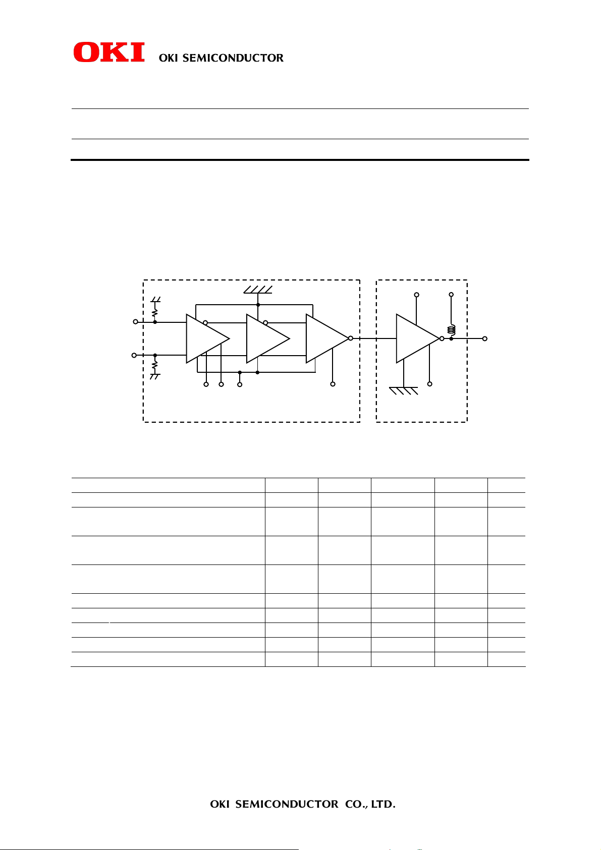
OUT IN
VB1 VB2 VS VC1
INB
VD
VCS
TO
October 1, 2008
ODHKGL4146-09
KGL4146
11.3 Gbps Modulator Driver IC
FEATURES
• High Output Voltage: Maximum Amplitude up to 6.0 Vpp
• X-Point Control Functio n
• Output Amplitude Control Function
• Integrated Bias Inductor
FUNCTION DIAGRAM
ABSOLUTE MAXIMUM RATINGS
Supply Voltage*1 VS -6.5 0.3 V
X-Point Control Voltage VB1
X-Point Reference Voltage VB2
Internal Amplitude Control Voltage VC1 -6.5
Cascode FET Gate Voltage VCS -1.0 0.3 x VD V
DC Bias for Output Stage Amplifier VD 0 5.5 V
Allowable Current of Output Stage ID_MAX 250 mA
Operating Temperature at Package Base Ts -10 100 °C
Storage Temperature Tst -40 125 °C
*1 Please keep VS below 0V, during power of VD supplied.
Pre-Driver
Parameter Symbol Min Max Unit Note
VS-4.5
(Min. -6.5)
VS-4.5
(Min. -6.5)
Booster-Amp
VS+2.4
(Max. 0.3)
VS+2.4
(Max. 0.3)
VS+1.2
(Max. 0.3)
V
V
V
1/6

ODHKGL4146-09
KGL4146
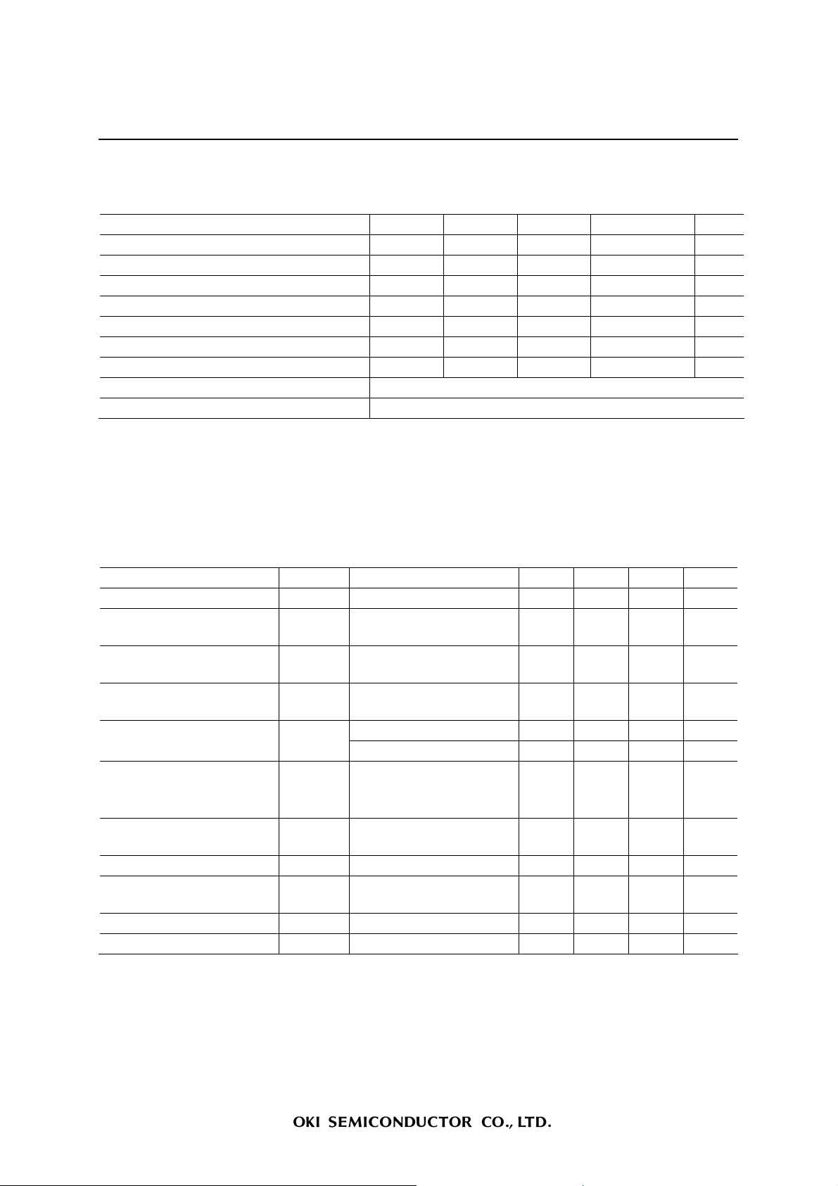
RECOMMENDED OPERATING CONDITIONS
Parameter Symbol Min Typ Max Unit
Supply Voltage VS -5.46 -4.94 V
X-Point Control Voltage VB1 VS+0.8 VS+1.7 V
X-Point Reference Voltage*1 VB2 -4.2 -3.95 -3.7 V
Internal Amplitude Control Voltage VC1 VS VS+1.0 V
Cascode FET Gate Voltage*2 VCS 0 0.25 x VD V
DC Bias for Output Stage Amplifier
Operating Temperature at Package Base Ts 0 85 °C
Input Interface AC coupled (External blocking capacitor is required)
Output Interface AC coupled (External blocking capacitor is required)
*3, 4
VD 0.5 5.0 V
*1 VB2 can be open.
For VB2 opened, VB2 is biased at about –3.95V (VS=-5.2V).
*2 VCS can be open.
For VCS opened, VCS is biased at about 1.2V (VD=5.0V).
*3 Output Amplitude can be tuned by control voltage VD.
*4 External inductor for low frequency is required.
ELECTRICAL CHARACTERISTICS
Parameter Symbol Condition Min Typ Max Unit
Maximum Input Data Rate NRZ 11.3 Gbps
Supply Current of VS Iss
Supply Current of VD*1 ID
Power Consumption Pwr
Input Amplitude Vin
Output Amplitude (Max) Vo (Max)
Output Amplitude (Min) Vo (Min)
X-Point Control Xp NRZ , 50 load 40 60 %
Output Rise/Fall Time Tr/Tf
Input Return Loss S11 100kHz–10 GHz 13 dB
Output Return Loss S22 100kHz–10 GHz 13 dB
*1 External inductor for low frequency is required
VC1=VS+1V, VCS: Open,
Xp=50%
VC1=VS+1V, VCS: Open,
Xp=50%
Vo=6Vpp, VC1=VS+1V,
VCS: Open, Xp=50%
Differential (AC Coupled) 0.2 1 Vpp
Single-Ended (AC Coupled)
50 load, AC Coupled,
VD=5V, VC1=VS+1V,
VCS : Open, Xp=50%
50 load, AC Coupled,
Xp=50%
50 load,
20%-80%
110 mA
180 mA
1.3 W
0.4 1 Vpp
5.5 6.0 Vpp
3.0 3.5 Vpp
40 ps
2/6
 Loading...