

Page 1
Electronic Components
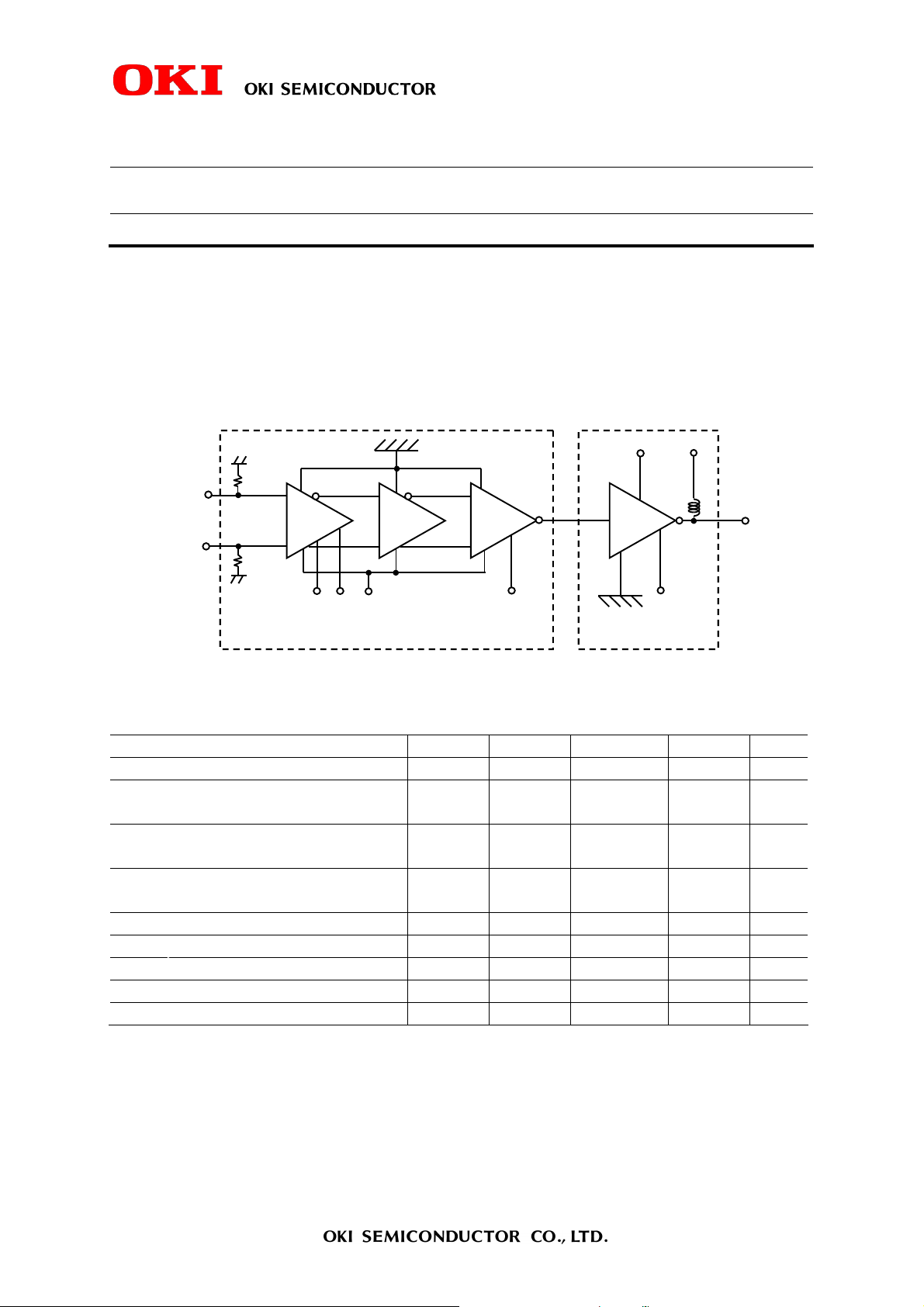
OUT IN
VB1 VB2 VS VC1
INB
VD
VCS
TO
October 1, 2008
ODHKGL4146-09
KGL4146
11.3 Gbps Modulator Driver IC
FEATURES
• High Output Voltage: Maximum Amplitude up to 6.0 Vpp
• X-Point Control Functio n
• Output Amplitude Control Function
• Integrated Bias Inductor
FUNCTION DIAGRAM
ABSOLUTE MAXIMUM RATINGS
Supply Voltage*1 VS -6.5 0.3 V
X-Point Control Voltage VB1
X-Point Reference Voltage VB2
Internal Amplitude Control Voltage VC1 -6.5
Cascode FET Gate Voltage VCS -1.0 0.3 x VD V
DC Bias for Output Stage Amplifier VD 0 5.5 V
Allowable Current of Output Stage ID_MAX 250 mA
Operating Temperature at Package Base Ts -10 100 °C
Storage Temperature Tst -40 125 °C
*1 Please keep VS below 0V, during power of VD supplied.
Pre-Driver
Parameter Symbol Min Max Unit Note
VS-4.5
(Min. -6.5)
VS-4.5
(Min. -6.5)
Booster-Amp
VS+2.4
(Max. 0.3)
VS+2.4
(Max. 0.3)
VS+1.2
(Max. 0.3)
V
V
V
1/6
Page 2
ODHKGL4146-09
KGL4146
RECOMMENDED OPERATING CONDITIONS
Parameter Symbol Min Typ Max Unit
Supply Voltage VS -5.46 -4.94 V
X-Point Control Voltage VB1 VS+0.8 VS+1.7 V
X-Point Reference Voltage*1 VB2 -4.2 -3.95 -3.7 V
Internal Amplitude Control Voltage VC1 VS VS+1.0 V
Cascode FET Gate Voltage*2 VCS 0 0.25 x VD V
DC Bias for Output Stage Amplifier
Operating Temperature at Package Base Ts 0 85 °C
Input Interface AC coupled (External blocking capacitor is required)
Output Interface AC coupled (External blocking capacitor is required)
*3, 4
VD 0.5 5.0 V
*1 VB2 can be open.
For VB2 opened, VB2 is biased at about –3.95V (VS=-5.2V).
*2 VCS can be open.
For VCS opened, VCS is biased at about 1.2V (VD=5.0V).
*3 Output Amplitude can be tuned by control voltage VD.
*4 External inductor for low frequency is required.
ELECTRICAL CHARACTERISTICS
Parameter Symbol Condition Min Typ Max Unit
Maximum Input Data Rate NRZ 11.3 Gbps
Supply Current of VS Iss
Supply Current of VD*1 ID
Power Consumption Pwr
Input Amplitude Vin
Output Amplitude (Max) Vo (Max)
Output Amplitude (Min) Vo (Min)
X-Point Control Xp NRZ , 50 load 40 60 %
Output Rise/Fall Time Tr/Tf
Input Return Loss S11 100kHz–10 GHz 13 dB
Output Return Loss S22 100kHz–10 GHz 13 dB
*1 External inductor for low frequency is required
VC1=VS+1V, VCS: Open,
Xp=50%
VC1=VS+1V, VCS: Open,
Xp=50%
Vo=6Vpp, VC1=VS+1V,
VCS: Open, Xp=50%
Differential (AC Coupled) 0.2 1 Vpp
Single-Ended (AC Coupled)
50 load, AC Coupled,
VD=5V, VC1=VS+1V,
VCS : Open, Xp=50%
50 load, AC Coupled,
Xp=50%
50 load,
20%-80%
110 mA
180 mA
1.3 W
0.4 1 Vpp
5.5 6.0 Vpp
3.0 3.5 Vpp
40 ps
2/6
Page 3

ODHKGL4146-09
1
12 9.3 9.9
10.9±0.3
13 19
18-0.65
4-0.65
20-0.3
2-7.5 20 31 32 38
20 31 19 13 12 1 32 38
0.9
0.9
K4146
INDEX
0.775
0.775
PACKAGE DIMENSIONS PIN ASSIGNMENT
4-0.5
10-0.2
(Lot No)
8-0.65
0.15
0.655
(Top View)
6.4
2- 4.6
7.0
2.5(max)
(Bottom View)
1.0
0.655
Symbol
No.
1 GND Ground
2 GND Ground
3 VC1
4 GND Ground
5 VCS
6 GND Ground
7 GND Ground
8.0±0.3
8 GND Ground
9 GND Ground
10 VD
11 GND Ground
12 GND Ground
13 GND Ground
14 GND Ground
15 GND Ground
16 GND Ground
17 GND Ground
18 Out Signal Output Port
19 GND Ground
20 GND Ground
21 GND Ground
22 GND Ground
23 GND Ground
24 GND Ground
25 TO
26 GND Ground
27 GND Ground
28 VS Supply Voltage Port
29 VB2
30 VB1 X-Point Control Port
31 GND Ground
32 GND Ground
33 INB Inverted Input Port
34 GND Ground
35 GND Ground
36 GND Ground
37 IN Signal Input Port
38 GND Ground
KGL4146
Note
Internal Amplitude
Control Port
Cascode FET Gate
Bias Port
Output Stage Amplifier
DC Bias Port
Output Termination
Port
X-Point Reference
Port
1.0
This package is non-hermetic.
Unit: mm
3/6
Page 4

ODHKGL4146-09
GND
VD
Su
pply Voltage
MZ Mod.
TYPICAL APPLICATION
Output Stage Amplifier DC Bias
typ. 150
Inductor
>100H
Inverted Data Input
Blocking
Capacitor
Ex. 0.1F
Data Input
INB
OUT
KGL4146
VB1
VC1 VB2
VS
TO
VCS
X-Point Control
Internal Amplitude Control
X-Point Reference
Cascode FET Gate Bias
Chip
Capacitor
0.1F
TO port: Do not connect voltage source and ground.
APPLICATION NOTE
1. For stable operation;
a) To prevent a dependence of “X-Point” on the supply voltage VS,
Case 1 : VB2 is open
VB2 is biased at about 0.76 x VS (-3.95V@VS=-5.2V) by the internal circuit.
Control VB1, so that the voltage difference “VB1–VB2” is constant.
Case 2 : VB2 is biased
Bias VB2 by using the external voltage source independent of VS.
Control VB1 by using the external voltage source independent of VS.
Blocking
Capacitor
Ex. 0.1F
KGL4146
50
4/6
Page 5

ODHKGL4146-09
b) To prevent a dependence of “Output amplitude” on the supply voltage VS
Control the voltage of “VC1”, so that the voltage difference “VC1–VS” is constant.
2. Power-up/shut-down sequence;
For power-up, supply control voltages (VB1, (VB2), VC1) at first, second VS, next VD then VCS.
For shut-down, VCS at first, next VD, next VS, then control voltages.
Customer does not need to care about the sequence for the control voltages (VB1, (VB2), VC1).
KGL4146
5/6
Page 6

ODHKGL4146-09
KGL4146
SAFETY AND HANDLING INFORMATION ON GaAs DEVICES
Arsenic Compound (GaAs Devices)
The product contains arsenic (As) as a compound.
This material is stable for normal use, however, its dust or vapor may be potentially hazardous to the human
body.
Avoid ingestion, fracture, burning or chemical treatment to the product.
• Do not put the product in your mouth.
• Do not burn or destroy the product.
• Do not perform chemical treatment for the product.
Keep laws and ordinances related to the disposal of the products.
ESD CONSIDERATIONS
This device can be da maged by ESD; t herefore appropriate precautions must be taken to avoid exposure to ESD
and EOS during handling, assembly, and testing of these devices. Failure to adhere to proper ESD/EOS
precautions during handling and assembly of these devices can damage or adversely affect device reliability.
NOTICE
1. The information contained herein can change without notice owing to product and/or technical improvements.
Before using the product, please make sure that the information being referred to is up-to-date.
2. The outline of action and examples for application circuits described herein ha ve been chosen as an
explanation for the standard action and performance of the product. When planning to use the product, please
ensure that the external conditions are reflected in the actual circuit, assembly, and program designs.
3. When designing your product, please use our pr oduct below the specified maximum ratings a nd within the
specified operating ranges including, but not limited to, operating voltage, power dissipation, and operating
temperature.
4. OKI SEMICONDUCTOR as sumes no responsibility or liability whatsoever for any failure or unusual or
unexpected operation resulting from misuse, neglect, improper installation, repair, alteration or accident,
improper handling, or unusual physical or electrical stress including, but not limited to, exposure to
parameters beyond the specified maximum ratings or operation outside the specified operating range.
5. Neither indemnity against nor license of a third party’s industrial and intellectual property right, etc. is
granted by us in connection with the use of the product and/or the information and drawings contained herein.
No responsibility is assumed by us for any infringement of a third party’s right which may result from the use
thereof.
6. The products listed in this document are intended for use in general electronics equipment for co mmercial
applications (e.g., o ffice auto mation, co mmunication e quipment, measurement equipment, co nsumer
electronics, etc.). These products are not authorized for use in any system or application that requires special
or enhanced quality and reliability characteristics nor in any system or application where the failure of s uch
system or application may result i n the l oss or damage of property, or death or injury to humans.
Such applications include, but are not limited to, traffic and automotive equipment, safety devices, aerospace
equipment, nuclear power control, medical equipment, and life-support systems.
7. Certain products in this document may need government approval before they can be exported to particular
countries. The purchaser assumes the responsibility of determining the legality of export of these products
and will take appropriate and necessary steps at their own expense for these.
8. No part of the contents contained herein may be reprinted or reproduced without our prior permission.
Copyright 2008 OKI SEMICONDUCTOR CO., LTD.
6/6
 Loading...