1
Electronic Components
ODHKGL4136HD-04
February 18, 2004
KGL4136HD
10.7 Gbps Differential Mach-Zehnder Modulator Driver IC
FEATURES
• Differential Output Voltag e: Maximum Ampl itude > 7.4 Vpp ( 3.7Vpp Each)
• X-Point Control Function
• Output Amplitude Control Function
APPLICATIONS
SONET OC-192 Transmission Systems up to 10.7 Gbps
DWDM Systems
Long Haul and Ultra Long Haul Transmission Systems
Optical Transmitters/Transceivers/Transponders
GENERAL DESCRIPTIONS
The KGL4136HD is a high perfo rmance Mach Zehnder Modul ator driver for SONET/SDH up to
10.7Gb/s. The device pr ov id es a Different ial o utp ut ampli t ud e > 7.4Vpp ( single ended >3.7Vpp
each ), output amplitude control, and duty cycle (X-Point) control.
The KGL4136HD data inp ut accepts single ende d or differential AC-coupl ed signals.
Capacitors for AC Termination and Blocking Capacitors are Required. External
BiasTees are Required to provide output DC Bias (VD). The device provides a minimum of
Differential 7.4Vpp output amplitude AC coupled to a 50-ohm load. The output ampl itude can be
tune d by va rying VC1.
The KGL4136HD is capable of adjusting the crossing point (X-point) from 40% to 60% of the
output eye diagram via the differential voltage between VB1 and VB2.
The KGL4136HD is packaged in a high performance 32-pin 7mm QFP package.
KGL4136HD BLOCK DIAGRAM
External
INB
IN
VB1 VB2 VS VC1
OUTB
OUT
1/9

1
Electronic Components
ABSOLUTE MAXIMUM RATINGS
Supply Voltage VS -6.5 0.3 V
X-Point Control Voltage VB1
X-Point Reference Voltage VB2
Output Amplitude Control Voltage VC1 -6.5
DC Bias for Output Stage Amplifier VD VS/2 0.3 V
Operating Temperature at Package Base Ts -10 100 °C
Storage Temperature Tst -40 125 °C
RECOMMENDED OPERATING CONDITIONS
Supply Voltage VS -5.46 -5.2 -4.94 V
Supply Voltage*1 VD Vs+3 -1.5 0 V
X-Point Control Voltage VB1 VS+0.8 VS+2.2 V
X-Point Reference Voltage
Output Amplitude Control Voltage VC1 VS VS+1.0 V
Input Amplitude ( Differential ) 0.25 1 Vpp
Input Amplitude ( Single Ended )
Operating Temperature at Package Base Ts 0 85 °C
Input Interface AC coupled (External blocking capacitor is required)
Output Interface AC coupled (External Bias-T is required for VD)
*1 VD is supplied at Output Port using External Bias-T.
*2 VB2 can be open or biased by the external circuit.
For VB2 opened, VB2 is biased at about –3.95V ( VS=-5.2V ).
ELECTRICAL CHARACTERISTICS
Parameter Symbol Condition Min Typ Max Unit
Input Data Rate NRZ 10.7 Gbps
Supply Current of VS Iss 200 250 mA
Supply Current of VD ID @VD=-1.5V 100 150 mA
Pwer Dissipation Pw 1 W
Output Amplitude (Max)
X-Point Control Xp NRZ, 50 Ω load 40 60 %
Output Rise/Fall Time Tr/Tf 50 Ω load, 20%-80% 40 ps
Input Return Loss S11 100kHz–10 GHz 13 dB
Note) Equation of power Dissipation is
Pw = |VS * I
*1 Output Amplitude (Max) is defined as each value of Out and Outb .
ODHKGL4136HD-04
KGL4136HD
Parameter Symbol Min Max Unit Note
VS-4.5
(Min. -6.5)
VS-4.5
(Min. -6.5)
Parameter Symbol Min Typ Max Unit
*2
VB2
Vin
*1
Vo (Max) @VC1=VS+1V,VD=-1.5V,Xp≅50% 3.7 4.0 Vpp
| – |VD * ID |
SS
-4.2 -3.95 -3.7
0.5 1 Vpp
VS+2.4
(Max. 0.3)
VS+2.4
(Max. 0.3)
VS+1.2
(Max. 0.3)
V
V
V
V
2/9

ODHKGL4136HD-04
∼∼∼∼
∼∼∼∼
y
y
y
y
∼∼∼∼
∼∼∼∼
y
1
Electronic Components
Power Suppl
KGL4136HD
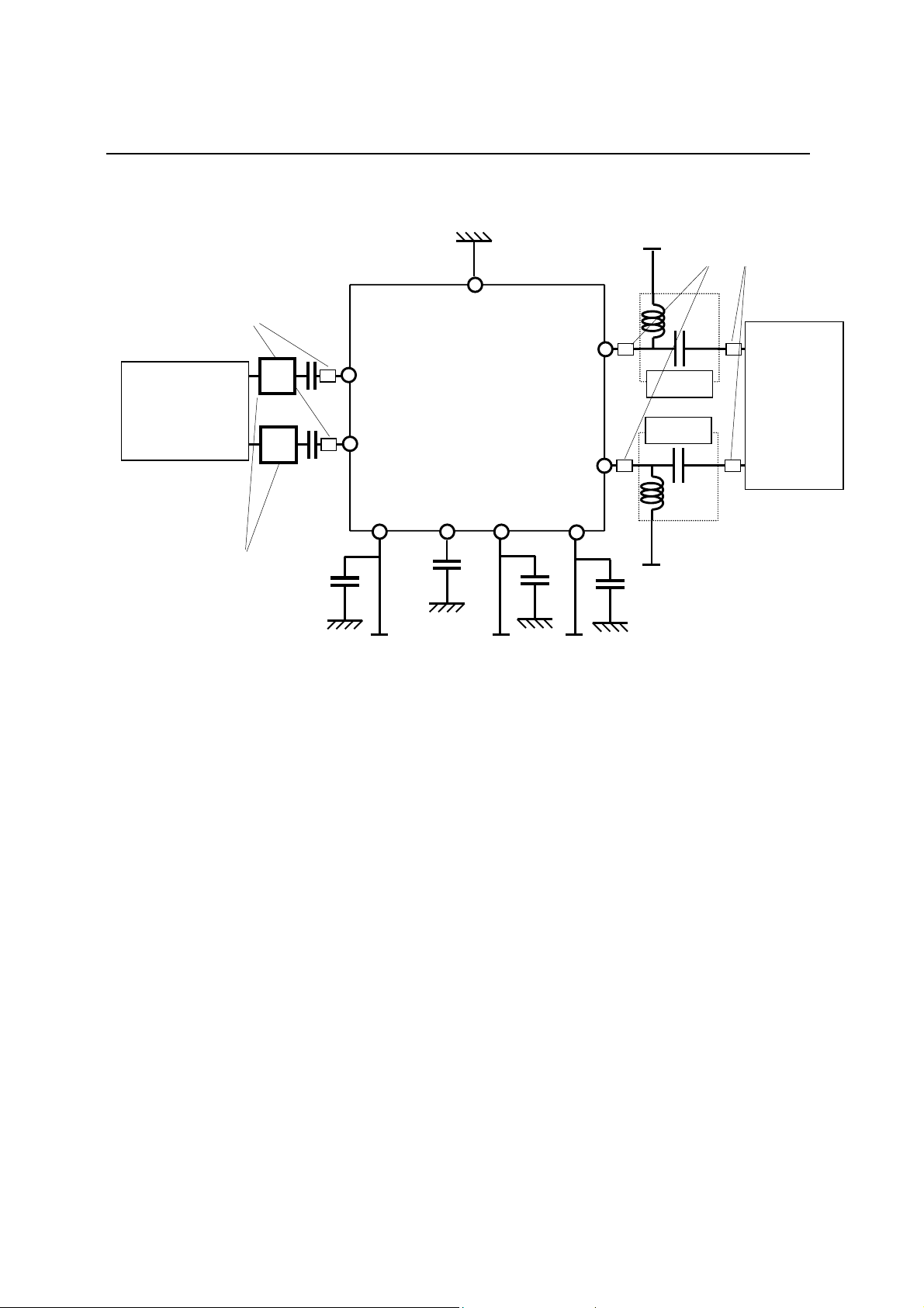
AC CHARACTERISTICS TEST CIRCUIT
50Ω Transmission Line
PULSE
PATTERN
GENERATOR
Blocking
Capacitor
Fc=7.5GHz
Bessel
Filter
0.1µF
VB1
0.1µF
(VB1)
Power Suppl
GND
KGL4136HD
VB2 VS VC1
0.1µF
(VS)
Power Suppl
Power Suppl
(VC1)
0.1µF
(VD)
(VD)
Power Suppl
Bias-T
Bias-T
50Ω Transmission Line
OSCILLO
-SCOPE
3/9
 Loading...