

Page 1

1
Electronic Components
ODHKGL4136HD-04
February 18, 2004
KGL4136HD
10.7 Gbps Differential Mach-Zehnder Modulator Driver IC
FEATURES
• Differential Output Voltag e: Maximum Ampl itude > 7.4 Vpp ( 3.7Vpp Each)
• X-Point Control Function
• Output Amplitude Control Function
APPLICATIONS
SONET OC-192 Transmission Systems up to 10.7 Gbps
DWDM Systems
Long Haul and Ultra Long Haul Transmission Systems
Optical Transmitters/Transceivers/Transponders
GENERAL DESCRIPTIONS
The KGL4136HD is a high perfo rmance Mach Zehnder Modul ator driver for SONET/SDH up to
10.7Gb/s. The device pr ov id es a Different ial o utp ut ampli t ud e > 7.4Vpp ( single ended >3.7Vpp
each ), output amplitude control, and duty cycle (X-Point) control.
The KGL4136HD data inp ut accepts single ende d or differential AC-coupl ed signals.
Capacitors for AC Termination and Blocking Capacitors are Required. External
BiasTees are Required to provide output DC Bias (VD). The device provides a minimum of
Differential 7.4Vpp output amplitude AC coupled to a 50-ohm load. The output ampl itude can be
tune d by va rying VC1.
The KGL4136HD is capable of adjusting the crossing point (X-point) from 40% to 60% of the
output eye diagram via the differential voltage between VB1 and VB2.
The KGL4136HD is packaged in a high performance 32-pin 7mm QFP package.
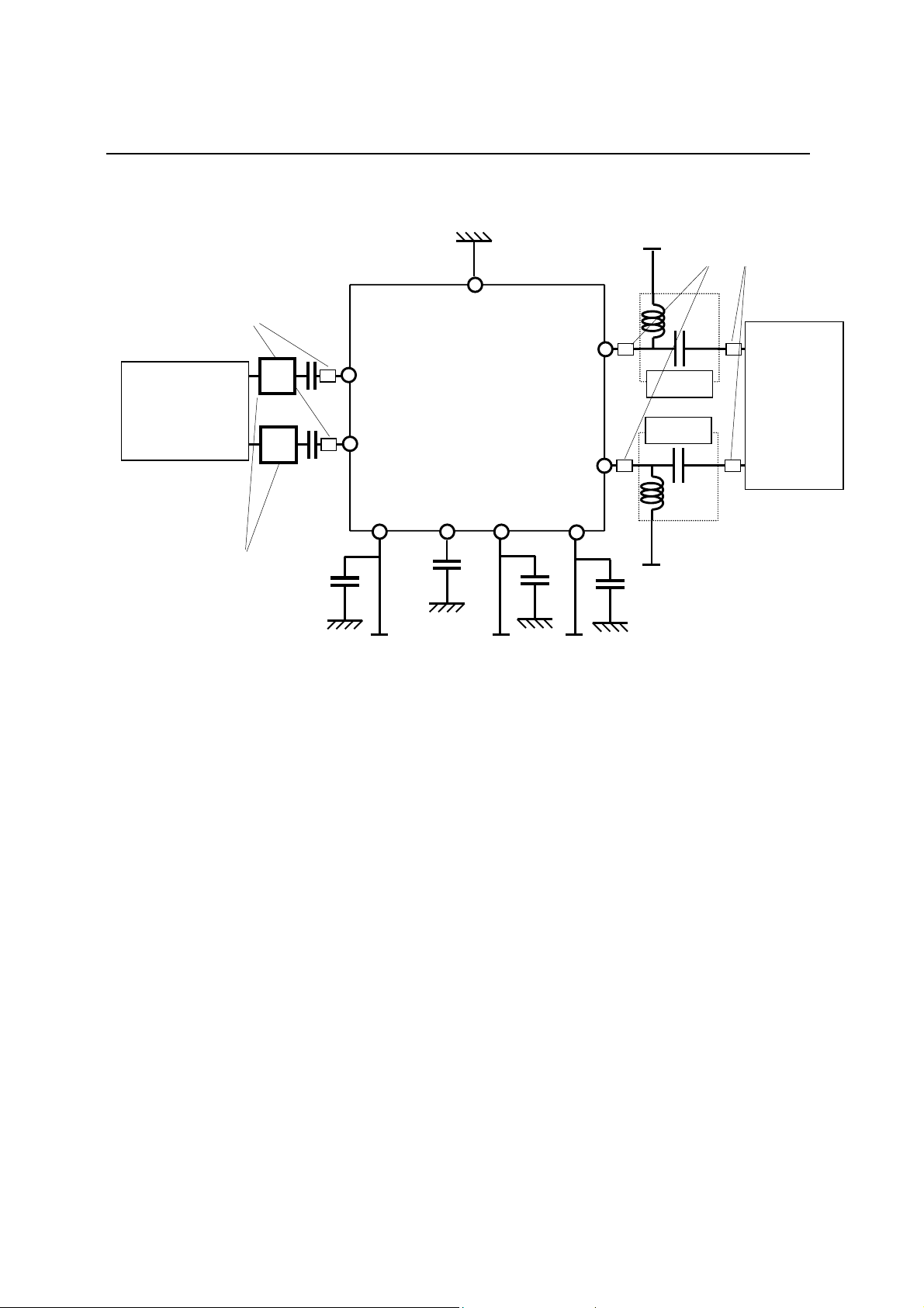
KGL4136HD BLOCK DIAGRAM
External
INB
IN
VB1 VB2 VS VC1
OUTB
OUT
1/9
Page 2
1
Electronic Components
ABSOLUTE MAXIMUM RATINGS
Supply Voltage VS -6.5 0.3 V
X-Point Control Voltage VB1
X-Point Reference Voltage VB2
Output Amplitude Control Voltage VC1 -6.5
DC Bias for Output Stage Amplifier VD VS/2 0.3 V
Operating Temperature at Package Base Ts -10 100 °C
Storage Temperature Tst -40 125 °C
RECOMMENDED OPERATING CONDITIONS
Supply Voltage VS -5.46 -5.2 -4.94 V
Supply Voltage*1 VD Vs+3 -1.5 0 V
X-Point Control Voltage VB1 VS+0.8 VS+2.2 V
X-Point Reference Voltage
Output Amplitude Control Voltage VC1 VS VS+1.0 V
Input Amplitude ( Differential ) 0.25 1 Vpp
Input Amplitude ( Single Ended )
Operating Temperature at Package Base Ts 0 85 °C
Input Interface AC coupled (External blocking capacitor is required)
Output Interface AC coupled (External Bias-T is required for VD)
*1 VD is supplied at Output Port using External Bias-T.
*2 VB2 can be open or biased by the external circuit.
For VB2 opened, VB2 is biased at about –3.95V ( VS=-5.2V ).
ELECTRICAL CHARACTERISTICS
Parameter Symbol Condition Min Typ Max Unit
Input Data Rate NRZ 10.7 Gbps
Supply Current of VS Iss 200 250 mA
Supply Current of VD ID @VD=-1.5V 100 150 mA
Pwer Dissipation Pw 1 W
Output Amplitude (Max)
X-Point Control Xp NRZ, 50 Ω load 40 60 %
Output Rise/Fall Time Tr/Tf 50 Ω load, 20%-80% 40 ps
Input Return Loss S11 100kHz–10 GHz 13 dB
Note) Equation of power Dissipation is
Pw = |VS * I
*1 Output Amplitude (Max) is defined as each value of Out and Outb .
ODHKGL4136HD-04
KGL4136HD
Parameter Symbol Min Max Unit Note
VS-4.5
(Min. -6.5)
VS-4.5
(Min. -6.5)
Parameter Symbol Min Typ Max Unit
*2
VB2
Vin
*1
Vo (Max) @VC1=VS+1V,VD=-1.5V,Xp≅50% 3.7 4.0 Vpp
| – |VD * ID |
SS
-4.2 -3.95 -3.7
0.5 1 Vpp
VS+2.4
(Max. 0.3)
VS+2.4
(Max. 0.3)
VS+1.2
(Max. 0.3)
V
V
V
V
2/9
Page 3
ODHKGL4136HD-04
∼∼∼∼
∼∼∼∼
y
y
y
y
∼∼∼∼
∼∼∼∼
y
1
Electronic Components
Power Suppl
KGL4136HD
AC CHARACTERISTICS TEST CIRCUIT
50Ω Transmission Line
PULSE
PATTERN
GENERATOR
Blocking
Capacitor
Fc=7.5GHz
Bessel
Filter
0.1µF
VB1
0.1µF
(VB1)
Power Suppl
GND
KGL4136HD
VB2 VS VC1
0.1µF
(VS)
Power Suppl
Power Suppl
(VC1)
0.1µF
(VD)
(VD)
Power Suppl
Bias-T
Bias-T
50Ω Transmission Line
OSCILLO
-SCOPE
3/9
Page 4

1
Electronic Components
ODHKGL4136HD-04
KGL4136HD
PACKAGE DIMENSIONS
24 17
4.445
32-0.2
25
32
K4136
HD
Index
1 8
7.0±0.2
Note) This package is non-hermetic.
(Top View)
28-0.635
1.5±0.25
Unit : mm
16
9
Lot No.
0.62
0.125
7.0±0.2
0.4
PIN CONNECTIONS
No. Symbol Note
1 GND Ground
2 GND Ground
3 GND Ground
4 GND Ground
5 GND Ground
6 GND Ground
7 GND Ground
8 GND Ground
9 GND Ground
10 OUT Signal Output Port
11 GND Ground
12 GND Ground
13 OUTB Inverted Signal Output Port
14 GND Ground
15 GND Ground
16 GND Ground
17 GND Ground
18 GND Ground
19 VC1 Output Amplitude Control Port
20 VS Supply Voltage Port
21 VS Supply Voltage Port
22 VB2 Input Termination Port
23 VB1
0.75±0.2
24 GND Ground
25 GND Ground
26 GND Ground
27 GND Ground
28 INB Inverted Input Port
29 GND Ground
1.12±0.2
30 GND Ground
31 IN Signal Input Port
32 GND Ground
X-Point Control and Inverted
Input Termination Port
4/9
Page 5

1
Electronic Components
TYPICAL OPERATING CHARACTERISTICS
Measured Condition
Display Factor V : 1.0V/div, H : 20 ps/div, Offset : 0.0V
Input Signal
Waveform of OUT
Waveform of OUTB
ODHKGL4136HD-04
KGL4136HD
Operating Speed : 10.7Gbps
Input Amplitude : Differential 0.25Vpp , NRZ PRBS31 Through 7.5GHz Bessel Filter
Vs : -5.2V Is : 212.5mA
Vb1 : -3.929V
Vc1 : -4.2V
Vd : -1.5V Id : 111.0mA
Power : 0.938W
X-Point : 51.3%
Amplitude:
4.536pp
Tr : 32.9ps
Tf : 28.5ps
-
X-Point : 54.4%
Amplitude:
4.443Vpp
Tr : 29.3ps
Tf : 30.7ps
JitterP-P : 12.6ps
5/9
Page 6

1
µ
µ
. 0.
p
µ
h
h
Electronic Components
ODHKGL4136HD-04
KGL4136HD
TYPICAL APPLICATION CIRCUIT
NOTE: EXTERNAL BLOCKING CAPACITORS ARE REQUIRED FOR THE DATA INPUTS (IN/INB).
TERMINATION CAPACITORS ARE REQUIRED BETWEEN THE CONTROL VOLTAGES
(VB1/VB2) AND GROUND.
Supply Voltage of VD, or connect toground via resistor : 20-30
value depends on output amplitude.
Ω
whic
Chip
Capacitor
≥ 0.1
X-Point Control
F
VB1
GND
KGL4136HD
50Ω
OUTB
Inverted Data In
Blocking
Capacitor
Ex
1µF
ut
INB
Bias-T
Bias-T
MZ Mod.
Chip
Capacitor
≥ 0.1
F
VB2
VS
VC1
OUT
50Ω
value depends on output amplitude.
Supply Voltage of VD, or connect t o
ground via resistor : 20-30
Chip
Capacitor
≥ 0.1
F
Supply Voltage of VS
Output
Control
Amplitude
Ω
whic
6/9
Page 7

ODHKGL4136HD-04
1
Electronic Components
APPLICATION NOTES
KGL4136HD
1. EXTERNA L BLOCKING CAPACITORS ARE REQUIRED FOR THE DATA INPUTS
(IN/INB). TERMINATION CAPACITORS ARE REQUIRED BETWEEN THE
CONTROL VOLTAGES (VB1/VB2) AND GROUND.
2. To minimize the dependence of the “X-Point” on the supply voltage VS
a : VB2 is open
VB2 is biased at about 0.76 x VS (-3.8V@VS=-5.2V) by the internal circuit.
Control VB1, so that the voltage difference “VB1–VB2” is constant.
b : VB2 is biased
Bias VB2 at about 1.2V by using the external voltage source independent of VS.
Control VB1 by using the external voltage source independent of VS.
3. To minimize the dependence of “Output amplitude” on the supply voltage VS
Control the voltage of “VC1”, so that the voltage difference “VC1–VS” is constant.
4. Power-up/shut-down sequence
a. For manual power-up, turn on supply control voltages (VB1, VB2, VC1) at
first, next VS, then VD. For shutdown, turn off VD first, then VS, then
control voltages. The sequence for the control v oltages (VB1, VB2, VC1 ) is
not critical.
b. For simultaneous start up it is recommended that the delay between the
supply control voltages (VB1, VB2, VC1) and VS b e minimized, or that all
voltages be applied at the same time.
7/9
Page 8

ODHKGL4136HD-04
1
Electronic Components
Assembly and ESD Considerations
KGL4136HD
Mounting Process:
The heat sink on the backside of IC package is recommended to have a good thermal path to
the electrically grounding metal on the PC board using a conductive adhesive, such as silver
paste. If conductive adhesive is not used, a thin thermal and electrically conductive film is
recommended to between the IC and PC board.
Soldering Process:
Soldering such that the heating area is spatially confined only in the vicinity of IC leads is
recommended.
The soldering condition is either shorter than 10 seconds at the lead temperature of lower
than 260 degC, or shorter than 3 seconds at the temperature of lower than 310 degC.
During soldering, pre-heating of PC board is required. The recommended temperature is in
the range between 120 degC and 150 degC. If the temperature is lower than that, "solder
balls" may occur.
A soldering iron with electrical isolation higher than 10M ohm as well as a small leakage
voltage is recommended.
ESD Considerations:
This device can b e damaged by ESD; therefore appropriate precautions m ust be taken to
avoid exposure to ESD and EOS during handling, assembly, and testing of these devices.
Failure to adhere to prop er ESD/EOS precautions during handlin g and assembly of these
devices can damage or adversely affect device reliability.
SAFETY AND HANDLING INFORMATION FOR GaAs DEVICES
Arsenic Compound (GaAs Devices)
The product contains arsenic (As) as a compound.
This material is stable for normal use; however, its dust or vapor may be potentially hazardous to the human
body.
Avoid inge stion, fracture, bur n ing or chemical treatment to the prod uct.
• Do not put the product in your mouth.
• Do not burn or destroy the product.
• Do not perform chemical treatment for the product.
Keep la ws and ordinances related to the dispos al of the pr oducts.
8/9
Page 9

ODHKGL4136HD-04
1
Electronic Components
KGL4136HD
NOTICE
1. The information contained herein can change without notice owing to product and/or technical improvements.
Before using th e pr oduct, plea se ma k e su r e that the information being re fe rred to is up- to -date.
2. The outline of action and examples for application circuits descr ibed herein have been chose n as an explanation f or
the standard action and performance of the product. When planning to use the product, please ensure that the
external conditions are reflected in the actual circuit, assembly, and program designs.
3. When designing your product, please use our product below the specified maximum ratings and within the
specified operating ranges including, but not limited to, operating voltage, power dissipation, and operating
temperature.
4. Oki assumes no responsibility or liability whatsoever for any failure or unusual or unexpected operation resulting
from misuse, neglect, improper installation, repair, alteration or accident, improper handling, or unusual physical
or electrical stress including, but not limited to, exposure to parameters beyond the specified maximum ratings or
operation outside the specified operating range.
5. Neither indemnity against nor license of a third party’s industrial and intellectual property right, etc. is granted by
us in connection with the use of the product and/or the information and drawings contained herein. No
responsibility is assumed by us for any infringement of a third party’s right which may result from the use thereof.
6. The products listed in this document are intended for use in general electronics equipment for commercial
applications (e.g., office automation, communication equipment, measurement equipment, consumer electronics,
etc.). These products are not authorized for use in any system or application that requires special or enhanced
quality and reliability characteristics nor in any system or application where the failure of such system or
application may result in the loss or damage of property, or death or injury to humans.
Such applications include, but are not limited to, traffic and automotive equipment, safety devices, aerospace
equipment, nuclear power control, medical equipment, and life-support systems.
7. Certain products in this document may need government approval before they can be exported to particular
countries. The purchaser a ssumes the respons ibility of determining the lega lity of ex port of these product s and wil l
take appropriate and necessary steps at their own expense for these.
8. No part of the contents contained herein may be reprinted or reproduced without our prior permission.
Copyright 2004 Oki Electric Industry Co., Ltd.
9/9
 Loading...