1
Electronic Components
KGL4126FA
10.7 Gbps Mach-Zehnder Modulator Driver IC
FEATURES
ODHKGL4126FA-03
October 29, 2003
• High Output Voltage: Maximum Amplitude > 6.0 Vpp
• X-Point Control Function
• Output Amplitude Control Function
APPLICATIONS
! SONET OC-192 and SDH STM-64 Transmission Systems up to 10.7 Gbps
! DWDM Systems
! Optical Transmitters/Transceivers/Transponders
! SONET/SDH Test Equipment
GENERAL DESCRIPTION
The KGL4126FA is a high performance Mach Zehnder Modulator driver for SONET/SDH and
10GbE applications up to 10.7Gb/s. The device provides a single-ended output voltage > 6Vpp,
output amplitude control, and duty cycle (X-Point) control.
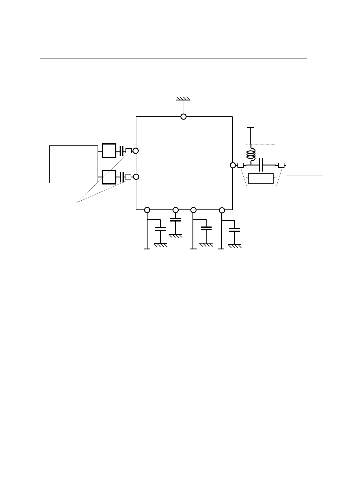
The KGL4126FA data input accepts single ended or differential AC-coupled signals. External
Capacitors for AC Termination and Blocking Capacitors are Required.
The device
provides a minimum of 6 Vpp output voltage AC coupled to a 50-ohm load. The output amplitude
can be tuned by varying VD, which is supplied at the output port using an external Bias-T.
The KGL4126FA is capable of adjusting the crossing point (X-point) from 45% to 55% of the
output eye diagram via the differential voltage between VB1 and VB2. The device specifications
are guaranteed for all crossing points from 45% to 55%.
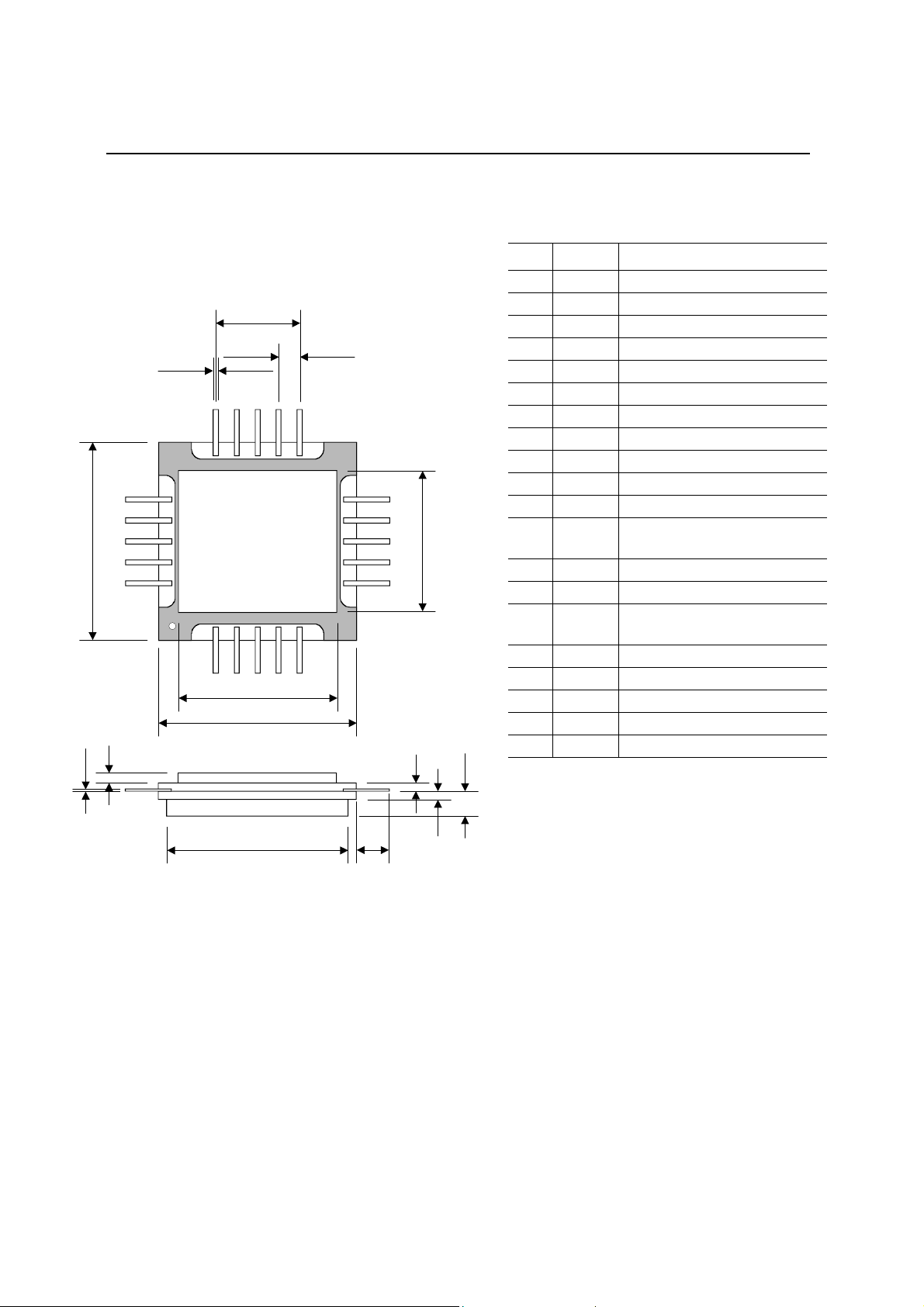
The KGL4126FA is packaged in a high performance 20-pin 12mm QFP package.
KGL4126FA B LOCK DIAGRAM
INB
IN
VB1 VB2 VS VC1
OUT
1/14

1
Electronic Components
ODHKGL4126FA-03
KGL4126FA
ABSOLUTE MAXIMUM RATINGS
Parameter Symbol Min Max Unit Note
Supply Voltage VS -6.5 0.3 V
X-Point Control Voltage VB1
Current Source FET Gate Bias Voltage VC1 -6.5
DC Bias for Output Stage Amplifier VD 0 5.0 V
Operating Temperature at Package Base Ts -10 100 °C
Storage Temperature Tst -40 125 °C
VS-4.5
(Min. -6.5)
VS+2.0
(Max. 0.3)
VS+1.2
(Max. 0.3)
V
V
RECOMMENDED OPERATING CONDITIONS
Parameter Symbol Min Typ Max Unit
Supply Voltage VS -5.46 -4.94 V
DC Bias for Output Stage Amplifier
X-Point Control Voltage VB1 VS+1.1 VS+1.5 V
Current Source FET Gate Bias Voltage
: Single – Ended
Operating Temperature at Package Base Ts 0 70 °C
Input Interface AC coupled (External blocking capacitor is required)
Output Interface AC coupled (External Bias-T is required for VD)
*1,2
VD 2.0 4.0 V
*1,3
VC1 VS VS+0.85 VS+1.0 V
Vin
0.25 1 Vpp Input Amplitude : Differential
0.5 1 Vpp
*1 Output amplitude can be tuned by control voltage VD.
*2 VD is supplied at Output Port using External Bias-T.
*3 It is recommended to set VC1 to a fixed value between VS+0.7V and VS+1.0V.
ELECTRICAL CHARACTERISTICS
Parameter Symbol Condition Min Typ Max Unit
Input Data Rate NRZ 10.7 Gbps
Supply Current of VS Iss X-Point : 45% - 55% 210 250 mA
Supply Current of VD ID Supply DC Bias by Bias-T 90 130 mA
Output Amplitude (Max) Vo (Max) 50 Ω load,(AC Coupled) 6.0 Vpp
X-Point Control Xp NRZ, 50 Ω load 45 55 %
Output Rise/Fall Time Tr/T f
Input Return Loss S11 100kHz–10 GHz 13 dB
50 Ω load
20%-80%
40 ps
2/14

1
∼∼∼∼
∼∼∼∼
y
y
y
∼∼∼∼
∼∼∼∼
y
Electronic Components
ODHKGL4126FA-03
KGL4126FA
AC CHARACTERISTICS TEST CIRCUIT
Power Suppl
Fc=7.5GHz
Bessel
Filter
GND
(VD)
PULSE
PATTERN
GENERATOR
KGL4126FA
OSCILLO
-SCOPE
Bias-T
50Ω Transmission Line
Blocking
Capacitor
VB1
VB2 VS VC1
0.1µF
0.1µF
0.1µF
50Ω Transmission Line
0.1µF
(VB1)
Power Suppl
(VS)
Power Suppl
Power Suppl
(VC1)
3/14

1
Electronic Components
ODHKGL4126FA-03
KGL4126FA
PACKAGE DIMENSIONS
20-0.3
15
16
12±0.2
20
KGL4126FA
1
JAPAN
XXX
1
0.6
0.125
5.08
9.6
12±0.2
PIN CONNECTIONS
No. Symbol Note
1 GND Ground
16-1.27
11
5
(Top View)
10
6
8.6
0.5
1.5
2 GND Ground
3 GND Ground
4 GND Ground
5 GND Ground
6 GND Ground
7 GND Ground
8 GND Ground
9 OUT. Signal Output and DC Bi as Port
10 GND Ground
11 GND Ground
12 VC1
13 VS Supply Voltage Port
14 VB2 Input Termination Port
15 VB1
16 GND Ground
17 INB Inverted Input Port
18 GND Ground
19 IN Signal Input Port
20 GND Ground
Current Source FET Gate Bias
Voltage
X-Point Control and Inverted
Input Termination Port
11
2±0.3
(Unit: mm)
0.5
4/14

1
p
Electronic Components
ODHKGL4126FA-03
KGL4126FA
TYPICAL OPERATING CHARACTERISTICS
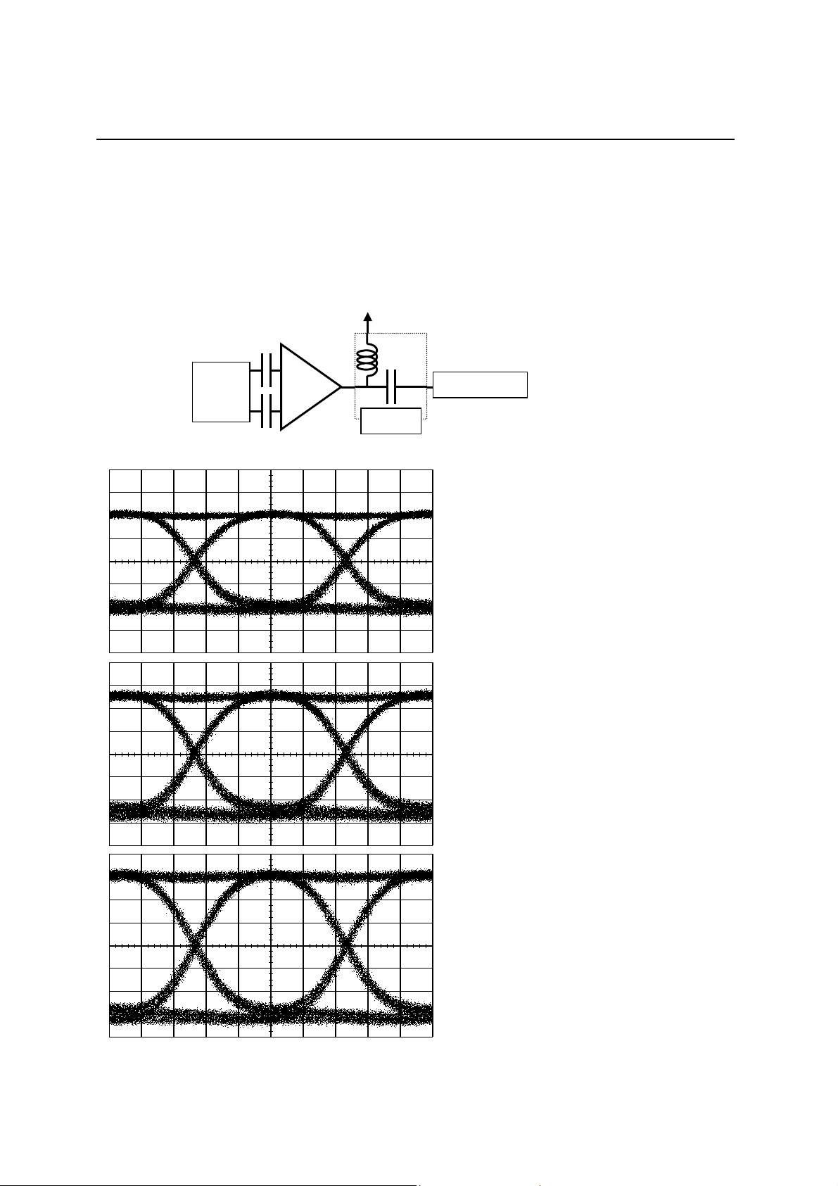
Measured Condition
Display Factor V : 1.0V/div, H : 20 ps/div, Offset : 0V
Input Signal
Tr/Tf(20-80%)≅36ps
10.7Gbps, NRZ , PN31, Diff erential 0.25Vpp, AC Coupled
( through 7.5GHz Bessel Filters )
Vd
PPG
KGL4126FA
Bias-T
Oscilloscope
Waveform @10.7Gbps Operate
Vs : -5.0V Is : 209.4mA
Vb1 : -3.8 00V Crossing-Point : 50. 3%
Vc1 : -4.0V
Vd : 2.39V Id : 55.5mA
Power : 1.180W
Amplitude:
4.007Vpp
Tr : 28.4ps
Tf : 27.6ps
JitterP-P : 10.4ps
Vs : -5.0V Is : 209.4mA
Vb1 : -3.785V Crossing-Point [%] : 50.6%
Vc1 : -4.0V
Vd : 3.04V Id : 72.3mA
Power : 1.267W
Amplitude:
5.009Vpp
Tr : 28.9ps
Tf [ps] : 28.9ps
JitterP-P : 10.2
s
Vs : -5.0V Is : 209.3mA
Vb1 : -3.7 60V Crossing-Point : 49. 8%
Vc1 : -4.0V
Vd : 3.78V Id : 89.1mA
Power : 1.383W
Amplitude:
6.004Vpp
Tr : 30.2ps
Tf : 31.6ps
-
Note Jitter(p-p) means “ 6 × Jitter(RMS) “.
5/14
 Loading...