

Page 1
1
Electronic Components
KGL4126FA
10.7 Gbps Mach-Zehnder Modulator Driver IC
FEATURES
ODHKGL4126FA-03
October 29, 2003
• High Output Voltage: Maximum Amplitude > 6.0 Vpp
• X-Point Control Function
• Output Amplitude Control Function
APPLICATIONS
! SONET OC-192 and SDH STM-64 Transmission Systems up to 10.7 Gbps
! DWDM Systems
! Optical Transmitters/Transceivers/Transponders
! SONET/SDH Test Equipment
GENERAL DESCRIPTION
The KGL4126FA is a high performance Mach Zehnder Modulator driver for SONET/SDH and
10GbE applications up to 10.7Gb/s. The device provides a single-ended output voltage > 6Vpp,
output amplitude control, and duty cycle (X-Point) control.
The KGL4126FA data input accepts single ended or differential AC-coupled signals. External
Capacitors for AC Termination and Blocking Capacitors are Required.
The device
provides a minimum of 6 Vpp output voltage AC coupled to a 50-ohm load. The output amplitude
can be tuned by varying VD, which is supplied at the output port using an external Bias-T.
The KGL4126FA is capable of adjusting the crossing point (X-point) from 45% to 55% of the
output eye diagram via the differential voltage between VB1 and VB2. The device specifications
are guaranteed for all crossing points from 45% to 55%.
The KGL4126FA is packaged in a high performance 20-pin 12mm QFP package.
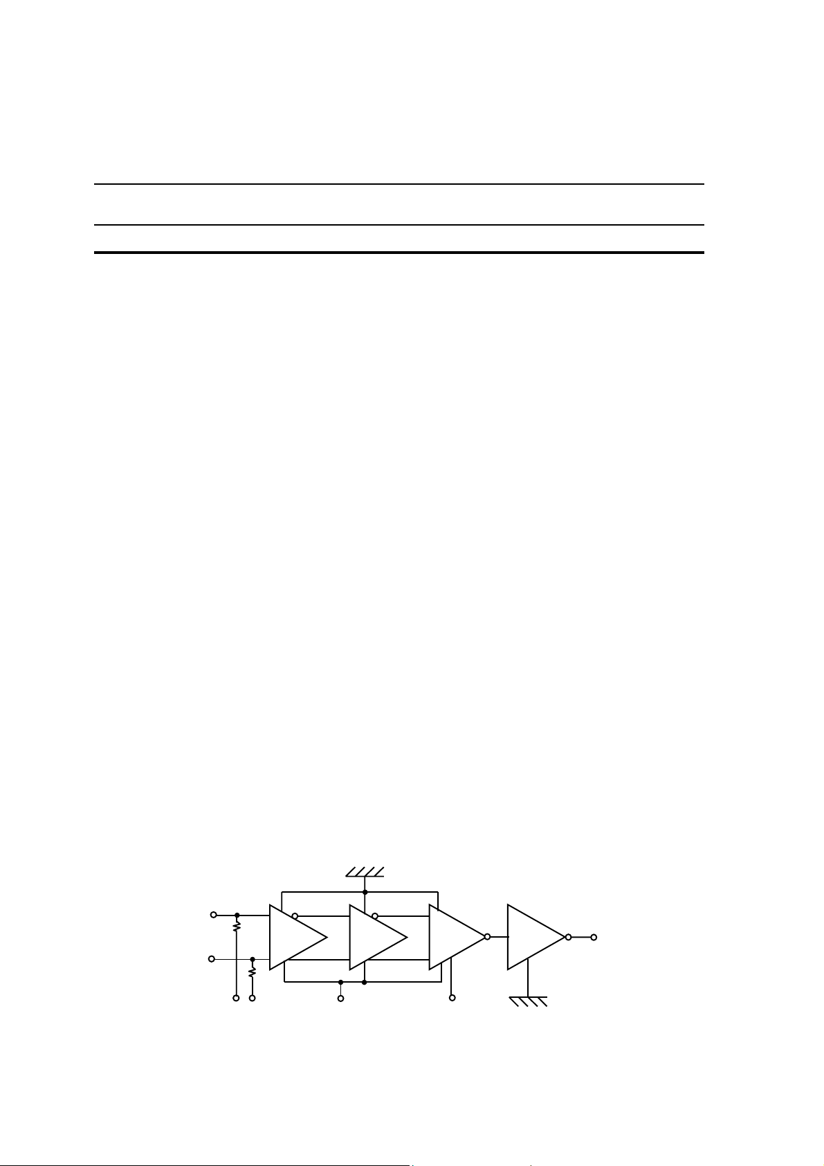
KGL4126FA B LOCK DIAGRAM
INB
IN
VB1 VB2 VS VC1
OUT
1/14
Page 2
1
Electronic Components
ODHKGL4126FA-03
KGL4126FA
ABSOLUTE MAXIMUM RATINGS
Parameter Symbol Min Max Unit Note
Supply Voltage VS -6.5 0.3 V
X-Point Control Voltage VB1
Current Source FET Gate Bias Voltage VC1 -6.5
DC Bias for Output Stage Amplifier VD 0 5.0 V
Operating Temperature at Package Base Ts -10 100 °C
Storage Temperature Tst -40 125 °C
VS-4.5
(Min. -6.5)
VS+2.0
(Max. 0.3)
VS+1.2
(Max. 0.3)
V
V
RECOMMENDED OPERATING CONDITIONS
Parameter Symbol Min Typ Max Unit
Supply Voltage VS -5.46 -4.94 V
DC Bias for Output Stage Amplifier
X-Point Control Voltage VB1 VS+1.1 VS+1.5 V
Current Source FET Gate Bias Voltage
: Single – Ended
Operating Temperature at Package Base Ts 0 70 °C
Input Interface AC coupled (External blocking capacitor is required)
Output Interface AC coupled (External Bias-T is required for VD)
*1,2
VD 2.0 4.0 V
*1,3
VC1 VS VS+0.85 VS+1.0 V
Vin
0.25 1 Vpp Input Amplitude : Differential
0.5 1 Vpp
*1 Output amplitude can be tuned by control voltage VD.
*2 VD is supplied at Output Port using External Bias-T.
*3 It is recommended to set VC1 to a fixed value between VS+0.7V and VS+1.0V.
ELECTRICAL CHARACTERISTICS
Parameter Symbol Condition Min Typ Max Unit
Input Data Rate NRZ 10.7 Gbps
Supply Current of VS Iss X-Point : 45% - 55% 210 250 mA
Supply Current of VD ID Supply DC Bias by Bias-T 90 130 mA
Output Amplitude (Max) Vo (Max) 50 Ω load,(AC Coupled) 6.0 Vpp
X-Point Control Xp NRZ, 50 Ω load 45 55 %
Output Rise/Fall Time Tr/T f
Input Return Loss S11 100kHz–10 GHz 13 dB
50 Ω load
20%-80%
40 ps
2/14
Page 3
1
∼∼∼∼
∼∼∼∼
y
y
y
∼∼∼∼
∼∼∼∼
y
Electronic Components
ODHKGL4126FA-03
KGL4126FA
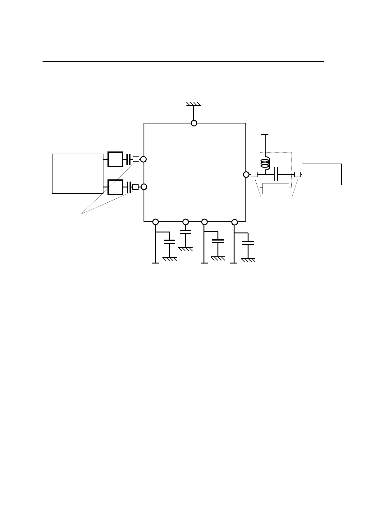
AC CHARACTERISTICS TEST CIRCUIT
Power Suppl
Fc=7.5GHz
Bessel
Filter
GND
(VD)
PULSE
PATTERN
GENERATOR
KGL4126FA
OSCILLO
-SCOPE
Bias-T
50Ω Transmission Line
Blocking
Capacitor
VB1
VB2 VS VC1
0.1µF
0.1µF
0.1µF
50Ω Transmission Line
0.1µF
(VB1)
Power Suppl
(VS)
Power Suppl
Power Suppl
(VC1)
3/14
Page 4
1
Electronic Components
ODHKGL4126FA-03
KGL4126FA
PACKAGE DIMENSIONS
20-0.3
15
16
12±0.2
20
KGL4126FA
1
JAPAN
XXX
1
0.6
0.125
5.08
9.6
12±0.2
PIN CONNECTIONS
No. Symbol Note
1 GND Ground
16-1.27
11
5
(Top View)
10
6
8.6
0.5
1.5
2 GND Ground
3 GND Ground
4 GND Ground
5 GND Ground
6 GND Ground
7 GND Ground
8 GND Ground
9 OUT. Signal Output and DC Bi as Port
10 GND Ground
11 GND Ground
12 VC1
13 VS Supply Voltage Port
14 VB2 Input Termination Port
15 VB1
16 GND Ground
17 INB Inverted Input Port
18 GND Ground
19 IN Signal Input Port
20 GND Ground
Current Source FET Gate Bias
Voltage
X-Point Control and Inverted
Input Termination Port
11
2±0.3
(Unit: mm)
0.5
4/14
Page 5
1
p
Electronic Components
ODHKGL4126FA-03
KGL4126FA
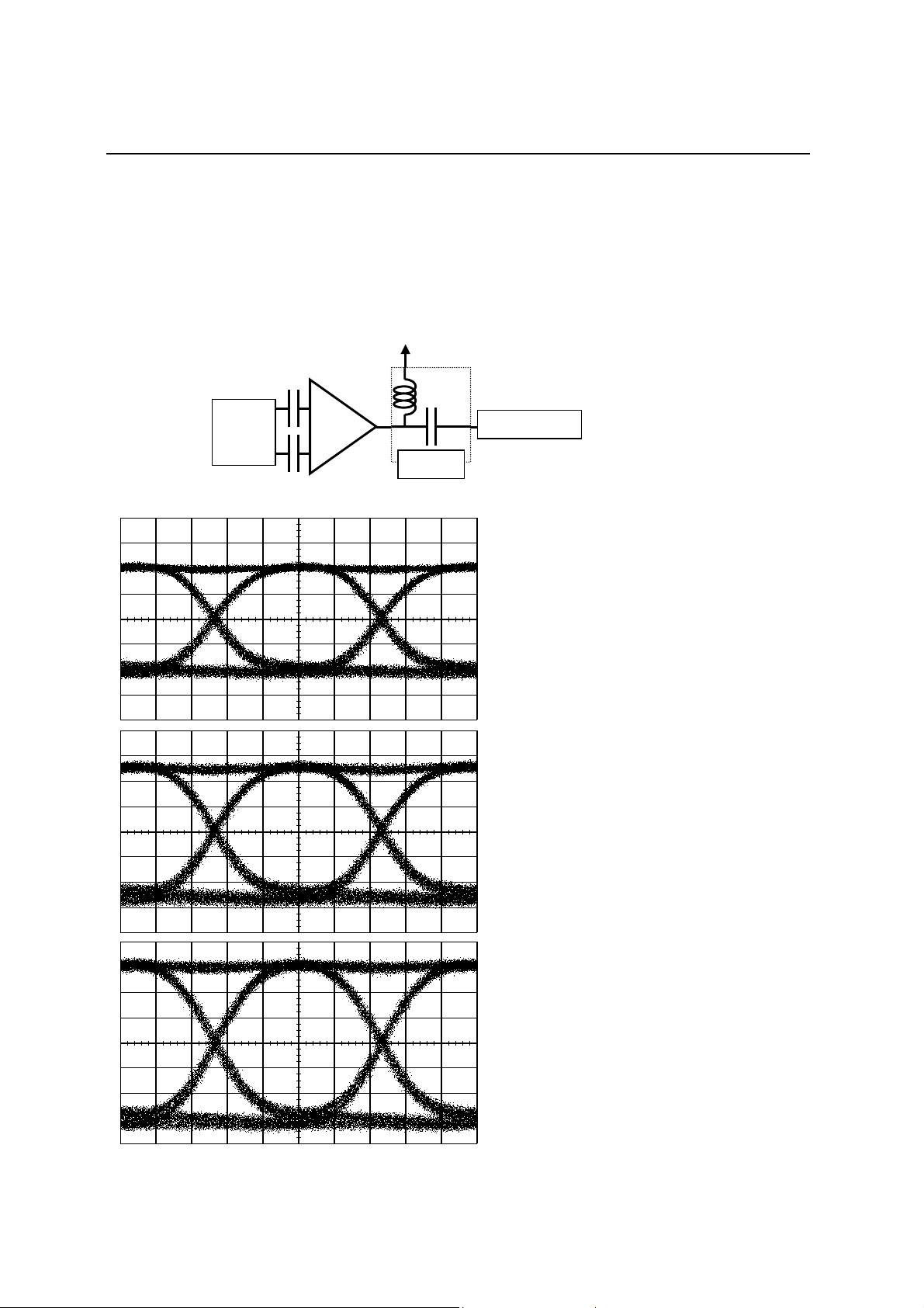
TYPICAL OPERATING CHARACTERISTICS
Measured Condition
Display Factor V : 1.0V/div, H : 20 ps/div, Offset : 0V
Input Signal
Tr/Tf(20-80%)≅36ps
10.7Gbps, NRZ , PN31, Diff erential 0.25Vpp, AC Coupled
( through 7.5GHz Bessel Filters )
Vd
PPG
KGL4126FA
Bias-T
Oscilloscope
Waveform @10.7Gbps Operate
Vs : -5.0V Is : 209.4mA
Vb1 : -3.8 00V Crossing-Point : 50. 3%
Vc1 : -4.0V
Vd : 2.39V Id : 55.5mA
Power : 1.180W
Amplitude:
4.007Vpp
Tr : 28.4ps
Tf : 27.6ps
JitterP-P : 10.4ps
Vs : -5.0V Is : 209.4mA
Vb1 : -3.785V Crossing-Point [%] : 50.6%
Vc1 : -4.0V
Vd : 3.04V Id : 72.3mA
Power : 1.267W
Amplitude:
5.009Vpp
Tr : 28.9ps
Tf [ps] : 28.9ps
JitterP-P : 10.2
s
Vs : -5.0V Is : 209.3mA
Vb1 : -3.7 60V Crossing-Point : 49. 8%
Vc1 : -4.0V
Vd : 3.78V Id : 89.1mA
Power : 1.383W
Amplitude:
6.004Vpp
Tr : 30.2ps
Tf : 31.6ps
-
Note Jitter(p-p) means “ 6 × Jitter(RMS) “.
5/14
Page 6

1
Electronic Components
TYPICAL OPERATING CHARACTERISTICS CONTINUED -
Output Amplitude De pe nde nce on Input Amplitude
(Vs=-5.2V,VB1:Xp≅50%@VD=4.0V,Vc1=-4.2V,VD=4.0V)
7.0
6.5
6.0
Am pl i t ude (V pp )
5.5
5.0
0 0.2 0.4 0.6 0.8
Rise Depende nce on I nput Ampli tude
(Vs=-5.2V,VB1:Xp≅50%@VD=4.0V,Vc1=-4.2V,VD=4.0V)
40
Input Amplitude (Vpp)
35
30
Tr (p s)
25
20
0 0.2 0.4 0.6 0.8
Is Dependence on Input Amplitude
(Vs=-5.2V,VB1:Xp≅50%@VD=4.0V,Vc1=-4.2V,VD=4.0V)
250
Input A m pl i t ude (V pp)
240
230
220
210
Supply Current : Is (mA)
200
0 0.2 0.4 0.6 0.8
Measured Condition
Input A m pl i t ude (V pp)
Input Signal -
10.7Gbps, NRZ, PN31, Differential 0.25Vpp, AC Coupled, Tr/Tf (20-80%)≅36ps
LotA
LotB
LotC
ODHKGL4126FA-03
KGL4126FA
Jitter Depende nce on I nput Amplitude
(Vs=-5.2V,VB1:Xp≅50%@VD=4.0V,Vc1=-4.2V,VD=4.0V)
20
15
10
JitterP-P (ps)
5
0
0 0.2 0.4 0.6 0.8
Input Ampl itu de (Vpp)
Fal l Ti m e De pe nde nce on I nput Amplitude
(Vs=-5.2V,VB1:Xp≅50%@VD=4.0V,Vc1=-4.2V,VD=4.0V)
40
35
30
Tf ( p s)
25
20
0 0.2 0.4 0.6 0.8
Input Ampl itu de (Vpp)
ID Dependence on Input Amplitude
(Vs=-5.2V,VB1:Xp≅50%@VD=4.0V,Vc1=-4.2V,VD=4.0V)
120
110
(mA )
D
100
90
80
Supply Current : I
70
0 0.2 0.4 0.6 0.8
Input Ampl itu de (Vpp)
LotA
LoyB
LotC
6/14
Page 7

1
)
A
Electronic Components
ODHKGL4126FA-03
KGL4126FA
TYPICAL OPERATING CHARACTERISTICS CONTINUED -
Output Amplitude De pe nde nce on V
(Vs=-5.2V,VB1:Xp≅50%@VD=4.0V,Vc1=-4.2V)
7.0
6.5
6.0
5.5
5.0
4.5
Am pl i t ude (V pp)
4.0
3.5
3.0
2.0 2.5 3.0 3.5 4.0
(V)
V
D
D
20
15
10
JitterP-P (ps)
5
0
2.0 2.5 3.0 3.5 4.0
Jitter Depende nce on V
(Vs=-5.2V,VB1:Xp≅50%@VD=4.0V,Vc1=-4.2V)
(V)
V
D
40
Rise Tim e Depende nce on V
(Vs=-5.2V,VB1:Xp≅50%@VD=4.0V,Vc1=-4.2V)
D
Fal l Ti m e Depende nce on V
(Vs=-5.2V,VB1:Xp≅50%@VD=4.0V,Vc1=-4.2V)
40
35
35
30
Tr (p s)
30
Tf (ps)
25
25
20
2.0 2.5 3.0 3.5 4.0
V
(V)
D
20
2.0 2.5 3.0 3.5 4.0
V
(V)
D
ID Dependence on V
50%@VD=4.0V,Vc1=-4.2V)
≅
250
240
230
(Vs=-5.2V,VB1:Xp
Is De pende nce on V
50%@VD=4.0V,Vc1=-4.2V)
≅
D
150
(mA
100
D
(Vs=-5.2V,VB1:Xp
220
210
Supply Current :Is (m
50
Suppl y Current : I
200
2.0 2.5 3.0 3.5 4.0
V
(V)
D
0
2.0 2.5 3.0 3.5 4.0
VD (V)
Input Signal -
10.7Gbps, NRZ, PN31, Differential 0.25Vpp, AC Coupled, Tr/Tf(20-80%)≅36ps
D
D
D
7/14
Page 8

1
)
Electronic Components
ODHKGL4126FA-03
KGL4126FA
TYPICAL OPERATING CHARACTERISTICS CONTINUED -
Tem pe rature Depe ndence of Output Amplitude
(Vs=-4.94V,VC1=-3.94V,VB1@Xp@50%,VB2=Open,VD=4V)
7.0
(Vs=-4.94V,VC1=-3.94V,VB1@Xp@50%,VB2=Open,VD=4V)
20
Tem pe rature Depende nce of Jitter
6.5
15
Am pl i t ude (V pp)
6.0
5.5
10
JitterP-P (ps)
5
5.0
-25 0 25 50 75 100
Temperature(°C)
0
-25 0 25 50 75 100
Temperature(°C)
Tempera ture De pe ndence of Rise Tim e
(Vs=-4.94V,VC1=-3.94V,VB1@Xp@50%,VB2=Open,VD=4V)
40
Tem pera ture De pendence of Fall Time
(Vs=-4.94V,VC1=-3.94V,VB1@Xp@50%,VB2=Open,VD=4V)
40
35
35
30
Tr (p s)
30
Tf (ps)
25
25
20
-25 0 25 50 75 100
Temperature(°C)
20
-25 0 25 50 75 100
Temperature(°C)
(Vs=-4.94V,VC1=-3.94V,VB1@Xp@50%,VB2=Open,VD=4V)
240
Tem pe ra ture Depe nde nce of I
S
(Vs=-4.94V,VC1=-3.94V,VB1@Xp@50%,VB2=Open,VD=4V)
Tem pera ture De pendence of I
120
D
230
220
110
(mA)
D
100
210
90
200
Supply Current :Is (mA
190
-25 0 25 50 75 100
Input Signal -
Temperature(°C)
10.7Gbps, NRZ, PN31, Differential 0.25Vpp, AC Coupled, Tr/Tf (20-80%)≅36ps
80
Suppl y Current : I
70
-25 0 25 50 75 100
Temperature(°C)
8/14
Page 9

1
Electronic Components
ODHKGL4126FA-03
KGL4126FA
TYPICAL OPERATING CHARACTERISTICS CONTINUED -
Output Amplitude De pe nde nce on Vs
(VC1=-3.94V,VB1@Xp@50%,VB2=Open,VD =4V)
7.0
6.5
(VC1=-3.94V,VB1@Xp@50%,VB2=Open,VD=4V)
20
15
Jitter Depende nce on Vs
Am pl i t ude (V pp)
6.0
5.5
10
JitterP-P (ps)
5
5.0
-5.5 -5.4 -5.3 -5.2 -5.1 -5.0 -4.9 -4.8 -4.7
40
Rise Tim e Depende nce on Vs
(VC1=-3.94V,VB1@Xp@50%,VB2=Open,VD =4V)
Vs (V)
0
-5.5 -5.4 -5.3 -5.2 -5.1 -5.0 -4.9 -4.8 -4.7
Vs (V)
Fal l Ti m e De pe nde nce on V s
(VC1=-3.94V,VB1@Xp@50%,VB2=Open,VD=4V)
40
35
35
30
Tr (p s)
25
30
Tf ( p s)
25
20
-5.5 -5.4 -5.3 -5.2 -5.1 -5.0 -4.9 -4.8 -4.7
Vs (V)
20
-5.5 -5.4 -5.3 -5.2 -5.1 -5.0 -4.9 -4.8 -4.7
Vs (V)
240
230
220
(VC1=-3.94V,VB1@Xp@50%,VB2=Open,VD =4V)
Is Dependence on Vs
(VC1=-3.94V,VB1@Xp@50%,VB2=Open,VD=4V)
120
110
(mA)
D
100
ID Dependence on Vs
210
90
200
Supply Current :Is (mA)
80
Suppl y Current : I
190
-5.5 -5.4 -5.3 -5.2 -5.1 -5.0 -4.9 -4.8 -4.7
Vs (V)
70
-5.5 -5.4 -5.3 -5.2 -5.1 -5.0 -4.9 -4.8 -4.7
Vs (V)
Input Signal -
10.7Gbps, NRZ, PN31, Differential 0.25Vpp, AC Coupled, Tr/Tf (20-80%)≅36ps
9/14
Page 10

1
0.
µ
. 0.
0.
Electronic Components
TYPICAL APPLICATION CIRCUIT
NOTE: EXTERNAL BLOCKING CAPACITORS ARE REQUIRED FOR THE DATA INPUTS (IN/INB).
TERMINATION CAPACITORS ARE REQUIRED BETWEEN THE CONTROL VOLTAGES (VB1/VB2) AND
GROUND.
Chip
Capacitor
≥
1µF
X-Point Control
Inverted Da ta Input
Blocking
Capacitor
Ex
1µF
Chip
Capacitor
F
≥ 0.1
VB2
KGL4126FA
GND
VS VC1
Supply Vo ltage of VS
Supply Voltage of VC1
Supply Vo ltage of VD
Bias-T
Chip
Capacitor
≥
1µF
ODHKGL4126FA-03
KGL4126FA
MZ Mod.
50
Ω
10/14
Page 11

1
Electronic Components
APPLICATION NOTES
ODHKGL4126FA-03
KGL4126FA
1. EXTERNAL BLOCKING CAPACITORS ARE REQUIRED FOR THE DATA INPUTS (IN/INB).
TERMINATION CAPACITORS ARE REQUIRED BETWEEN THE CONTROL VOLTAGES
(VB1/VB2) AND GROUND.
2. To minimize the dependence of the “X-Point” on the supply voltage VS
a. Use an external voltage source of –3.8V for “VB2”, or
b. Control the voltage of “VB1”, so that the voltage difference “VB1–VB2” is constant.
3. To minimize the dependence of “Output amplitude” on the supply voltage VS
a. It is recommended to set “VC1” to a fixed value between VS+0.7V and VS+1.0V. Control the
voltage of “VC1”, so that the voltage difference “VC1–VS” is constant.
b. The Output Amplitude can be tuned by adjusting VD; VD is supplied at the Output Port using an
External Bias-T.
4. Power-up/shut-down sequence
a. For manual power-up, turn on supply control voltages (VB1, VB2, VC1) at first, next
VS, then VD. For shutdown, turn off VD first, then VS, then control voltages. The
sequence for the control voltages (VB1, VB2, VC1) is not critical.
b. For simultaneous start up it is recommended that the delay between the supply
control voltages (VB1, VB2, VC1) and VS be minimized, or that all voltages be
applied at the same time.
11/14
Page 12

1
Electronic Components
ODHKGL4126FA-03
KGL4126FA
TYPICAL PWB LAYOUT and LAYOUT CONSIDERATIONS
To minimize crosstalk and signal losses, keep the connections between the KGL4126FA and the MZ
modulator as short as possible. Circuit boards should be manufactured wi th low-loss dielectrics. Use good
high frequency layout techniques and multi-layer boards with solid ground plane to minimize crosstalk and
EMI. Controlled impedance lines are required for the data inputs and output.
Board Material : Nelco4000_13S
(t=12mil, εr=3.3)
CPW gap:0.67mm
CPW width:0.6mm
Lead pitch:1.27mm
Lead width:0.3mm
Lead length:ex.L=2.0mm
In-B a r = >
In =>
KGL4126FA
CPW length:ex.L+0.15mm
(CPW nealy50
0.6mm
Ω)
=> OUT
It provides the area which
changes from the CPW
width into the MSL width.
Foot print of board
=15 to 45 degrees
θ
0.713mm
(MSLnealy 50
MSL w idth:0.713mm(28.07mil)
:Sign a l lin e
:Po w er line
:Ground line/plane
Ω)
12/14
Page 13

ODHKGL4126FA-03
1
Electronic Components
KGL4126FA
Assembly and ESD Considerations
Mounting Process:
! The heat sink on the backside of IC package is recommended to have a good thermal path to the
electrically grounding metal on the PC board using a conductive adhesive, such as silver paste. If
conductive adhesive is not used, a thin thermal and electrically conductive film is recommended to
between the IC and PC board.
Soldering Process:
! Soldering such that the heating area is spatially confined only in the vicinity of IC leads is
recommended.
! The soldering condition i s either shorter than 10 s econds at the l ead t emperature of lower than 260
degC, or shorter than 3 seconds at the temperature of lower than 310 degC.
! During soldering, pre-heating of PC board is required. The recommended temperature is in the
range between 120 degC and 150 degC. If the temperature is lower than that, "solder balls" may
occur.
! A soldering iron with electrical isolation higher than 10M ohm as well as a small leakage voltage is
recommended.
ESD Considerations:
! This device can be damaged by ESD; therefore appropriate precautions must be taken to avoid
exposure to ESD and EOS during handling, assembly, and testing of these devices. Failure to
adhere to proper ESD/EOS precautions during handlin g and assembl y of these devices can dama ge
or adversely affect device reliability.
13/14
Page 14

ODHKGL4126FA-03
1
Electronic Components
KGL4126FA
SAFETY AND HANDLING INFORMATION FOR GaAs DEVICES
Arsenic Compound (GaAs Devices)
The product contains arsenic (As) as a compound.
This material is stable for normal use; however, its dust or vapor may be potentially hazardous to the human body.
Avoid inge stion, fracture, burning or chemical trea tm e nt to the pro du ct.
• Do not put the product in your mouth.
• Do not burn or destroy the product.
• Do not perform chemical treatment for the product.
Keep la ws and ordin ances rel ated to the disposal of the produ cts.
NOTICE
1. The information contained herein can change without notice owing to product and/or technical improvements. Before using the
product, please make sure that the information being referred to is up-to-date.
2. The outline of action and examples for application circuits described herein have been chosen as an explanation for the standard
action and performance of the product. When planning to use the product, please ensure that the externa l conditions are reflected in
the actual circuit, assembly, and program designs.
3. When designing your product, please use our product below the specified maximum ratings and within the specified operating
ranges including, but not limited to, operating voltage, power dissipation, and operati ng temperature.
4. Oki assumes no responsibility or liability whatsoever for any failure or unusual or unexpected operation resulting from misuse,
neglect, improper installation, repair, alteration or accident, improper handling, or unusual physical or electrical stress including,
but not limited to, exposure to parameters beyond the specified maximum ratings or operation outside the specified operating
range.
5. Neither indemnity against nor license of a third par ty’s indu strial and inte llectual proper ty right, etc. is g ranted by us in con nection
with the use of the product and/or the information and drawings contained herein. No responsibility is assumed by us for any
infringement of a third party’s right which may result from the use thereof.
6. The products listed in this doc ument are intended for use in general e lectronics e quipment f or commercial ap plications (e.g., office
automation, communication equipment, measurement equipment, consumer electronics, etc.). These products are not authorized
for use in any system or application that requires special or enhanced quality and reliability characteristics nor in any system or
application where the failure of such system or application may result in the loss or damage of property, or death or injury to
humans.
Such applications include, but are not limited to, traffic and automotive equipment, safety devices, aerospace equipment, nuclear
power control, medical equipment, and life-support systems.
7. Certain products in this document may need government approval before they can be exported to particular countries. The
purchaser assumes the responsibility of determining the legality of export of these products and will take appropriate and
necessary steps at their own expense for these.
8. No part of the contents contained herein may be reprinted or reproduced without our prior permission.
Copyright 2002 Oki Electric Industry Co., Ltd.
14/14
 Loading...