

Page 1
E2Q0056-18-73
(
)
This version: Jul. 1998
Previous version: —
KGF2236¡ electronic components
¡ electronic components
KGF2236
Dual Monolithic GaAs Power FET
GENERAL DESCRIPTION
The KGF2236, housed in a SMD-type plastic package, is a dual monolithic GaAs power FET that
features high efficiency at 3 V. Since the KGF2236 is made up of Driver FET and Power FET, that
is good to develop smaller and lighter. The KGF2236 specifications are guaranteed to fixed
matching circuit of 3.5 V and 835 MHz; external impedance-matching circuit are also required.
The KGF2236 provides high efficiency 60% (typical) with a 31.5 dBm (min. @Pin=7 dBm) output
at 3.5 V. The device is optimized for transmitter-final-stage amplifiers in Portable Handy Phones
(PHPs) and other 3 V analog cellular phone.
FEATURES
• Dual monolithic GaAs Power FET
• High efficiency: 60% (typ.)
• High gain: 25 dB
• Specifications guaranteed to a fixed matching circuit at 3.5 V, 835 MHz
• Package: 16PSSOP
PACKAGE DIMENSIONS
5.5±0.12
16
6.4±0.2
5.0±0.120.70±0.2
1
0.65±0.1
(4.55)
0.22±0.1
9
8
0.25±0.1
1.1
(2.6)
(2.6)
(3.0)
Unit: mm
1/9
Page 2
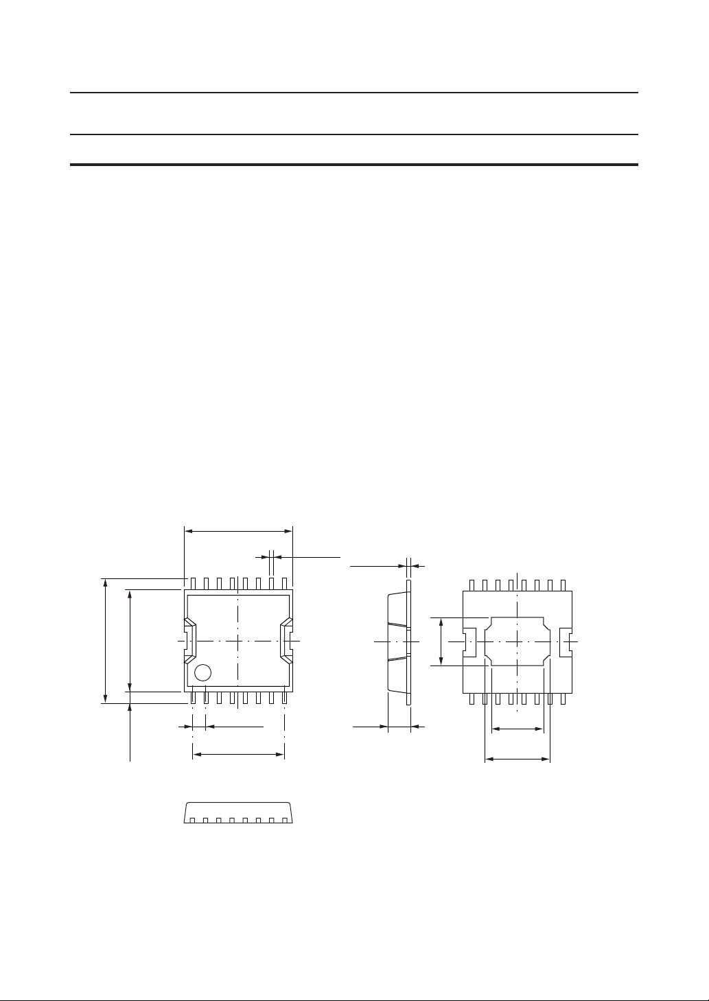
MARKING
KGF2236¡ electronic components
(16) (9)
CIRCUIT
K2236
X X X X
Index
(1) (8)
(3)
(1)
Q1
Production Name
Lot Number
Monthly Lot Number
Production Month (1–9, X, Y, Z)
Production Year (Lowest Digit)
(4)
(6)
Q2
(2)
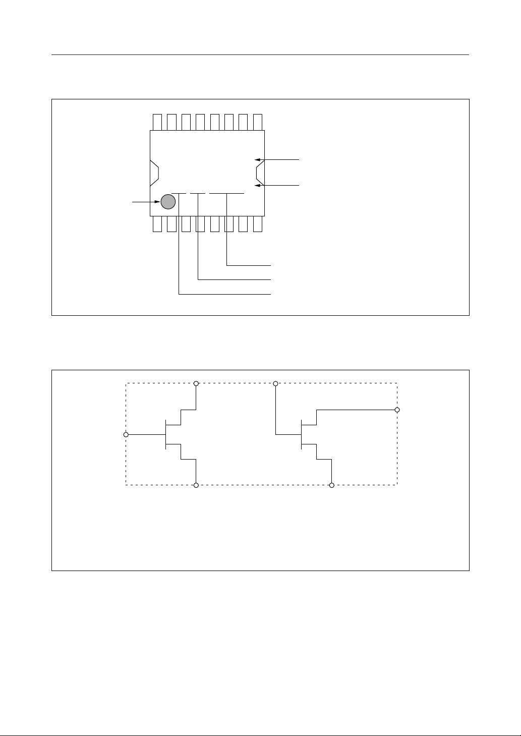
Q1: First stage (Driver-FET)
(1) Gate
(2) Source
(3) Drain
(5)
Q2: Final stage (Power-FET)
(4) Gate
(5) Source
(6) Drain
2/9
Page 3
KGF2236¡ electronic components
ABSOLUTE MAXIMUM RATINGS
Item Symbol Conditions Unit Min. Max. Notes
Drain-source voltage Q1V
Gate-source voltage Q1V
Drain current Q1I
Total power dissipation Q1P
Channel temperature Q1T
Drain-source voltage Q2V
Gate-source voltage Q2V
Drain current Q2I
Total power dissipation Q2P
Channel temperature Q2T
Storage temperature T
DSI
GSI
DSI
tot1
ch1
DS2
GS2
DS2
tot2
ch2
stg
Ta = 25°C V — 8.0
Ta = 25°C V –6.0 0.4
Ta = 25°C A — 1.0
Ta = Tc = 25°C W — 2.0
— °C — 150
T a= 25°C V — 8.0
Ta = 25°C V –6.0 0.4
Ta = 25°C A — 5.0
Ta = Tc = 25°C W — 5.0
— °C — 150
— °C –45 150
ELECTRICAL CHARACTERISTICS
Item Symbol Conditions Unit Min. Typ. Notes
Gate-source leakage current Q1I
Gate-drain cut-off voltage Q1V
Drain current Q1I
Gate bias Q point Q1V
Thermal resistance Q1R
Gate-source leakage current Q2I
Gate-drain cut-off voltage Q2V
Drain current Q2I
Gate bias Q point Q2V
Thermal resistance Q2R
GSS1
GDO1
DSS1
GSQ1
th1
GSS2
GDO2
DSS2
GSQ2
th2
Output Power P
Power added efficiency PAE *1 % 55 60
VGS = –6 V mA — —
IGD = –0.3 mA V –15 —
VDS = 1.5 V, VGS = 0 V A 0.4 —
VDS = 3.5 V, IDS = 80 mA V –2.5 —
Channel to Case °C/W — —
VGS = –6 V mA — —
IGD = –2.4 mA V –15 —
VDS = 1.5 V, VGS = 0 V A 4.0 —
VDS = 3.5 V, IDS = 200 mA V –2.8 —
Channel to Case °C/W — —
*1 dBm 31.5 — —
O
(Ta=25°C)
(Ta=25°C)
Max.
0.1
—
—
–1.5
50
0.1
—
—
–1.8
20
—
Q1+Q2
Q1+Q2
*1 Condition: f = 835 MHz, VDS = 3.5 V, I
DSQ1
= 80 mA, I
= 200 mA, PIN = 7 dBm
DSQ2
3/9
Page 4

RF CHARACTERISTICS
p
]
]
Macthing condition
KGF2236
G
G
G
S2
L2
Normalized source impedance of 1st-stage GS1 = 0.323 + j0.940
Normalized load impedance of 1st-stage GL1 = 0.046 + j0.487
Normalized source impedance of final-stage GS2 = 0.032 + j0.124
Normalized load impedance of final-stage GL2 = 0.088 + j0.035
Po and P.A.E. vs. Pin
33 80
31 70
29 60
27 50
Vds = 3.5 V
IdsQ1 = 80 mA
IdsQ2 = 200 mA
freq = 835 MHz
G
S1
L1
KGF2236¡ electronic components
25 40
23 30
21 20
Output Power Pout [dBm]
19 10
17
–12
33 70
32.5 67
32 64
31.5 64
31 58
Output Power Pout [dBm]
30.5 55
30
2.7
–7 –2
In
ut Power Pin [dBm
Pout and P.A.E. vs. Vds
f = 835 MHz
IdsQ1 = 80 mA
IdsQ2 = 200 mA
Macthing Condition:
(Refer to SS.3)
2.9 3.1 3.3 3.5 3.7 3.9
Drain Voltage Vds [V
Pout
P.A.E
38
[%]
Power Added Efficiency P.A.E.
0
[%]
Power Added Efficiency P.A.E.
52
4/9
Page 5

Typical S Parameters
a) 1st-stage
Freq(MHz)
1000.0
1050.0
1100.0
1150.0
1200.0
1250.0
1300.0
1350.0
1400.0
1450.0
1500.0
1550.0
1600.0
1650.0
1700.0
1750.0
1800.0 0.600 151.68 3.253 39.97
1850.0 0.606 147.99 3.181 37.21
1900.0 0.609 144.76 3.097 35.04
1950.0 0.614 141.40 3.033 32.51
2000.0 0.620 137.98 2.955 30.37
2050.0 0.626 134.71 2.893 27.94
2100.0 0.627 131.47 2.840 25.92
2150.0 0.631 128.46 2.767 23.48
2200.0 0.639 125.40 2.728 21.30
2250.0 0.643 122.49 2.647 19.14
2300.0 0.647 119.51 2.605 16.82
2350.0 0.648 116.88 2.545 14.68
2400.0 0.653 114.19 2.495 12.24
2450.0 0.658 111.77 2.442 10.22
2500.0 0.663 108.94 2.392 7.97
2550.0 0.670 106.67 2.358 5.94
2600.0 0.675 103.73 2.315 3.78
2650.0 0.681 101.35 2.262 1.54
2700.0 0.684 98.90 2.221 –0.49
2750.0 0.691 96.57 2.176 –2.76
2800.0 0.692 93.89 2.139 –4.80 –4.83 0.238 113.31
2850.0 0.699 91.72 2.094 –7.13 –5.96 0.242 110.89
2900.0 0.697 89.29 2.046 –9.00 –7.10 0.247 109.43
2950.0 0.703 87.18 2.014 –11.13 0.142 –7.83 0.252 106.83
3000.0 0.704 85.20 1.979 –12.55 0.142 –9.30 0.257 105.71
MAG(S11) ANG(S11) MAG(S21) ANG(S21) MAG(S12) ANG(S12) MAG(S22) ANG(S22)
500.0
550.0
600.0
650.0
700.0
750.0
800.0
850.0
900.0
950.0
0.803
0.777
0.754
0.732
0.710
0.691
0.674
0.655
0.640
0.626
0.611
0.602
0.607
0.598
0.598
0.598
0.594
0.592
0.592
0.592
0.592
0.592
0.593
0.594
0.593
0.596
–79.65
–86.44
–93.06
–99.64
–105.83
–111.89
–117.77
–123.68
–129.02
–134.49
–139.49
–143.59
–148.59
–153.79
–158.09
–163.18
–168.09
–172.47
–176.86
178.45
174.30
170.06
166.28
162.20
158.65
154.86
7.551
7.283
6.995
6.747
6.478
6.264
6.014
5.775
5.581
5.377
5.205
5.067
4.916
4.748
4.602
4.461
4.314
4.201
4.051
3.939
3.811
3.726
3.607
3.522
3.418
3.351
121.80
116.97
112.87
108.50 50.71
104.68
100.72
97.15
93.37
90.29
86.80
84.01
80.87
77.49
74.25
71.33
68.12
65.39
62.23
59.76
56.99
54.54
51.72
49.47
46.92
44.71
42.10
0.046
0.049
0.052
0.055
0.058
0.061
0.063
0.066
0.068
0.071
0.073
0.075
0.077
0.080
0.082
0.084
0.086
0.088
0.089
0.091
0.093
0.095
0.097
0.098
0.101
0.103
0.105
0.106
0.108
0.110
0.112
0.114
0.115
0.116
0.118
0.119
0.120
0.122
0.124
0.126
0.127
0.130
0.131
0.133
0.133
0.136
0.136
0.140
0.139
V
= 3.5 V, I
ds
57.85
55.44
52.83
0.161
0.155
0.150
0.146
48.67
46.84
45.03
43.36
41.84
40.27
38.66
37.29
35.94
34.55
33.12
31.80
30.33
29.00
27.66
26.33
25.17
23.91
22.90
21.69
20.74
19.56
0.141
0.137
0.133
0.129
0.127
0.124
0.123
0.121
0.120
0.120
0.120
0.121
0.122
0.123
0.125
0.126
0.128
0.131
0.133
0.135
0.137
0.140
18.35 0.144 165.25
16.97 0.149 162.39
15.80 0.153 158.55
14.40 0.158 155.75
12.96 0.162 152.56
11.70 0.167 148.91
10.45 0.171 145.65
9.53 0.175 142.86
8.31 0.180 139.92
7.45 0.183 137.25
6.18 0.187 134.67
5.37 0.190 132.42
4.30 0.196 130.47
3.24 0.199 128.17
2.27 0.207 126.08
0.90 0.210 123.59
–0.17 0.219 121.43
–1.51 0.221 119.29
–2.57 0.228 117.30
–3.64 0.232 115.04
KGF2236¡ electronic components
dsq
= 80 mA
–65.54
–70.86
–77.12
–82.97
–88.49
–94.20
–99.73
–105.03
–110.72
–115.88
–121.70
–126.59
–131.98
–136.85
–142.33
–147.08
–152.73
–157.16
–162.68
–166.83
–171.69
–175.90
179.98
176.35
172.09
168.92
5/9
Page 6

Typical S Parameters
V
= 3.50 (V), I
ds
= 80.0 (mA)
ds
Frequency : 0.5 to 3.0 GHz
Z0 = 50 W
KGF2236¡ electronic components
6/9
Page 7

Typical S Parameters
V
= 3.5 V, I
7.83
8.18
8.56
7.58
6.45
6.59
6.25
6.01
6.05
6.16
5.69
5.59
5.87
5.61
4.89
5.15
3.90
3.53
3.15
2.82
3.65
3.25
3.78
4.32
3.88
4.24
4.11
4.12
1.93
0.40
–2.41
–3.07
–1.81
–2.53
–2.33
–1.71
2.70
4.08
2.75
0.37
–2.00
–3.24
–3.49
–3.90
–4.74
–5.58
–5.23
–5.65
–4.77
–5.26
ds
0.822
0.819
0.817
0.819
0.819
0.820
0.818
0.819
0.821
0.820
0.819
0.821
0.820
0.819
0.820
0.819
0.819
0.819
0.821
0.822
0.820
0.822
0.820
0.819
0.818
0.815
0.817 145.28
0.818 144.31
0.819 143.21
0.819 142.17
0.814 140.99
0.819 139.85
0.817 138.84
0.817 137.56
0.818 136.51
0.814 135.35
0.808 134.29
0.810 133.62
0.810 132.58
0.814 131.47
0.813 130.45
0.812 129.12
0.813 128.21
0.814 126.97
0.816 125.91
0.814 124.68
0.814 123.64
0.813 122.24
0.810 121.19
0.815 119.99
b) final-stage
Freq(MHz)
1000.0
1050.0
1100.0
1150.0
1200.0
1250.0
1300.0
1350.0
1400.0
1450.0
1500.0
1550.0
1600.0
1650.0
1700.0
1750.0
1800.0 0.969
1850.0 0.972
1900.0 0.975
1950.0 0.974
2000.0 0.980
2050.0 0.984
2100.0 0.985
2150.0 0.983
2200.0 0.990
2250.0 0.990
2300.0 0.989
2350.0 0.992
2400.0 0.992
2450.0 0.997
2500.0 0.997
2550.0 1.001
2600.0 1.005
2650.0 1.004
2700.0 1.006
2750.0 1.010
2800.0 1.007 114.93
2850.0 1.009 113.64
2900.0 1.004 112.58
2950.0 1.008 111.30 –3.25 0.033
3000.0 1.009 110.46 –3.75 0.032 0.813 119.20
MAG(S11) ANG(S11) MAG(S21) ANG(S21) MAG(S12) ANG(S12) MAG(S22) ANG(S22)
500.0
550.0
600.0
650.0
700.0
750.0
800.0
850.0
900.0
950.0
0.935
0.937
0.937
0.940
0.938
0.941
0.943
0.945
0.947
0.950
0.953
0.952
0.949
0.952
0.951
0.948
0.953
0.951
0.952
0.954
0.957
0.961
0.963
0.967
0.967
0.967
–176.65
–179.20
178.60
176.23
174.29
172.33
170.53
168.81
166.92
165.31
163.44
161.67
160.21
158.74
157.35
155.83
154.54
153.00
151.80
150.48
149.14
147.76
146.50
145.17
143.78
142.22
141.10
139.76
138.43
137.14
135.81
134.56
133.22
131.84
130.51
129.43
127.82
126.66
125.26
124.30
122.90
121.62
120.23
119.10
117.76
116.36
2.455
2.237
2.055
1.899
1.772
1.658
1.560
1.467
1.402
1.330
1.279
1.240
1.177
1.125
1.081
1.025
0.991
0.955
0.919
0.881
0.856
0.829
0.807
0.780
0.766
0.745
0.724
0.703
0.685
0.671
0.656
0.642
0.631
0.615
0.603
0.591
0.578
0.570
0.559
0.554
0.542
0.536
0.526
0.517
0.508
0.503
0.492
0.486
0.474
81.67
79.34
77.42
75.32 7.49
73.37
71.64
69.69
68.06
66.37
64.65
62.95
60.83
57.95
56.33
53.90
52.12
50.63
48.50
46.93
45.41
43.84
42.24
40.73
39.28
37.55
35.85
34.14
32.47
30.83
29.25
27.87
26.22
24.64
22.99
21.33
20.03
18.51
16.64
15.34
13.50
11.91
10.21
8.64
6.84
5.39
3.18
1.89
–0.12
–1.35
0.022
0.022
0.022
0.022
0.023
0.023
0.023
0.023
0.023
0.023
0.023
0.024
0.024
0.024
0.024
0.025
0.025
0.025
0.025
0.025
0.025
0.025
0.025
0.025
0.026
0.027
0.027
0.027
0.028
0.029
0.029
0.029
0.028
0.028
0.028
0.027
0.027
0.027
0.029
0.031
0.031
0.032
0.031
0.032
0.032
0.033
0.032
0.032
0.032
0.469
0.460
KGF2236¡ electronic components
= 200 mA
dsq
172.25
171.09
170.05
168.82
167.93
166.84
165.89
164.70
163.80
162.61
161.59
160.67
159.87
158.52
157.56
156.47
155.72
154.52
153.49
152.42
151.50
150.42
149.33
148.04
147.19
146.40
7/9
Page 8

Typical S Parameters
V
= 3.50 (V), I
ds
= 200.0 (mA)
ds
Frequency : 0.5 to 3.0 GHz
Z0 = 50 W
KGF2236¡ electronic components
8/9
Page 9

Test Circuit Board for KGF2236
KGF2236¡ electronic components
Test Circuit
L4
C10
100000pF
C2
10pF
33nH
C9
10pF
C3
10pFC410.5pF
1
GND
2
V
D2
3
V
D2
4
V
D2
KGF2236
5
GND GND
6
GND GND
7
GND V
8
V
G1
GND
V
V
GND
GND
16
15
G2
14
G2
13
12
11
10
D1
9
L3
56nHR2100W
C8
C7
7pF
15pF
L2
33nH
RF
V
V
RF
D2
out
C11
39pF
G1
in
R1
100WL156nH
C1
39pF
Remarkable
Power Up
1) Begin by setting all power supplies to zero volts, and input power to –30 dBm.
2) Make sure that the RF input power is turned off.
3) Turn on VG1 (Pin 8) and VG2 (Pin 14 and 15) to (–) 3.3 V.
4) Adjust VD1 (Pin 10) and VD2 (Pin 2, 3 and 4) to V
5) Adjust VG1 and VG2 to I
= 80 mA and I
DSQ1
DSQ2
DS1
= V
= 3.5 V, respectively.
DS2
= 200 mA, respectively.
6) Turn RF on and adjust input power (Pin = 7 dBm) to get Pout = 31.5 dBm.
C5
100000pF
C6
39pF
V
G2
V
D1
Power down
To power down the device follow the above procedure in reverse order.
9/9
 Loading...