


E2Q0039-38-71
This version: Jul. 1998
Previous version: Jan. 1998
KGF1322S¡ electronic components
¡ electronic components
KGF1322S
Power FET (Ceramic Package Type)
GENERAL DESCRIPTION
The KGF1322S, housed in a SMD-type ceramic package, is a discrete UHF-band power FET that
features high efficiency, high output power, and low current operation. The KGF1322S specifications are guaranteed to a fixed matching circuit for 5.8 V and 850 MHz; external impedancematching circuits are also required. Because of its high efficiency, high output power (more than
33 dBm), and SMD package, the KGF1322S is ideal as a transmitter-final-stage amplifier for
personal handy phones, such as digital cellular phones.
FEATURES
• High output power: 33 dBm (min.)
• High efficiency: 60% (min.)
• Low thermal resistance: 18°C/W (typ.)
• Package: 3PFP
1/7
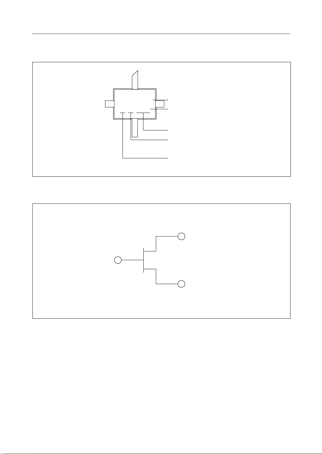
MARKING
KGF1322S¡ electronic components
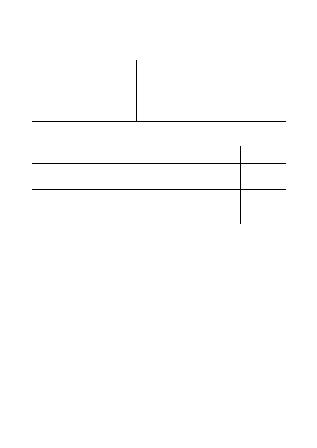
(1)
CIRCUIT
(2)
Gate(1)
K1322S
X X X X
(3)
PRODUCT NAME
LOT NUMBER
MONTHLY LOT NUMBER
PRODUCTION MONTH
(1-9,X,Y,Z)
PRODUCTION YEAR
(LOWEST DIGIT)
Drain(3)
(1) Gate
(2) Source
(3) Drain
Source(2)
2/7
ABSOLUTE MAXIMUM RATINGS
KGF1322S¡ electronic components
Item
Drain-source voltage
Gate-source voltage
Drain current I
Total power dissipation
Channel temperature
Storage temperature T
Symbol Condition Max.Unit
V
DS
V
GS
DS
P
tot
T
ch
stg
Ta = 25°C
Ta = 25°C
V
V
Ta = 25°C 3A —
Ta = Tc = 25°C
—
W
°C
— 125°C
Min.
—
–6.0
—
—
–45
ELECTRICAL CHARACTERISTICS
Item
Gate-source leakage current 0.1mA —VGS = –6 V —
Gate-drain leakage current 0.5mA —VGD = –16 V —
Drain-source leakage current 1.5mA —VDS = 10 V, VGS = –6 V —
Drain current —A 2.0VDS = 1.5 V, VGS = 0 V —
Gate-source cut-off voltage –2.6V –3.6VDS = 3 V, IDS = 4 mA —
Output power —dBm
Thermal resistance R
*1 Condition: f = 850 MHz, V
Symbol Condition Max.Unit
I
GSS
I
GDO
I
DS(off)
I
DSS
V
GS(off)
P
O
D
th
= 5.8 V, I
DS
(*1), P
(*1), P
= 22 dBm
IN
= 22 dBm %
IN
= 240 mA
DSQ
°C/W ——18Channel to case
Min.
33.0
60
Typ.
—
—Drain efficiency h
10
0.4
5
150
(Ta = 25°C)
—
3/7

RF CHARACTERISTICS
KGF1322S¡ electronic components
4/7

Typical S Parameters
Freq(MHz)
1000.0
1100.0
1200.0
1300.0
1400.0
1500.0
1600.0
1700.0
1800.0
1900.0
2000.0
2100.0
2200.0
2300.0
2400.0
2500.0
2600.0
2700.0
2800.0
2900.0
3000.0
MAG(S11) ANG(S11) MAG(S21) ANG(S21) MAG(S12) ANG(S12) MAG(S22) ANG(S22)
500.0
600.0
700.0
800.0
900.0
0.943
0.944
0.942
0.942
0.942
0.941
0.940
0.940
0.938
0.938
0.937
0.936
0.933
0.931
0.933
0.926
0.929
0.927
0.927
0.925
0.920
0.921
0.920
0.917
0.912
0.919
–153.04
–157.98
–161.54
–164.34
–166.64
–168.72
–170.35
–171.81
–173.25
–174.54
–175.88
–177.17
–178.32
–179.53
179.35
178.33
176.84
175.82
174.60
173.16
172.29
170.85
169.67
168.50
167.06
166.01
4.260
3.585
3.097
2.748
2.449
2.206
2.010
1.857
1.719
1.604
1.504
1.416
1.335
1.269
1.205
1.149
1.098
1.055
1.013
0.978
0.945
0.915
0.890
0.863
0.839
0.821
93.86
90.21
86.61
83.68
81.07
78.36
76.08
73.71
71.28
69.12
66.93
64.58
62.71
60.49
58.57
56.56
54.26
52.60
50.44
48.46
46.58
44.62
43.21
41.46
39.76
38.08
0.031
0.031
0.032
0.033
0.033
0.034
0.034
0.035
0.035
0.036
0.037
0.038
0.038
0.039
0.040
0.041
0.042
0.042
0.042
0.043
0.043
0.045
0.045
0.046
0.046
0.047
19.02
18.11
17.24
16.97
16.92
16.90
16.95
17.22
17.36
17.23
17.43
17.16
16.98
17.41
17.46
17.41
17.19
16.54
17.14
16.90
16.80
16.89
16.48
16.41
16.76
17.11
V
DS
= 5.8 V, I
0.694
0.694
0.694
0.704
0.704
0.699
0.698
0.704
0.704
0.703
0.701
0.699
0.699
0.703
0.701
0.701
0.698
0.700
0.699
0.695
0.700
0.701
0.710
0.709
0.704
0.703
KGF1322S¡ electronic components
= 240 mA
DS
–175.73
–177.31
–178.07
–178.36
–179.24
179.92
179.22
178.93
178.24
177.44
176.59
176.20
175.71
175.32
174.50
173.76
173.06
172.48
171.55
171.19
170.62
169.84
169.06
168.12
167.03
166.26
5/7

Typical S Parameters
V
= 5.8 V, I
DS
= 240 mA
DS
Frequency : 0.5 to 3.0 GHz
Z0 = 50 W
KGF1322S¡ electronic components
6/7

PACKAGE DIMENSIONS
KGF1322S¡ electronic components
3.8±0.15
3.5±0.15
1.9± 0.15
3.0±0.15
6.3±0.15
0.5±0.05
4.4±0.15
0.125±0.05
5.6 MAX
1.1±0.2
0.51±0.15
4.2±0.15
1.5±0.15
3.7±0.15
2.80
2.05
2.85
METALIZATION
2.0
(Unit: mm)
3.4
Package material
Lead frame material
Pin treatment
plate thickness
Al20
3
Fe-Ni-Co alloy
Ni/Au plating
Au:1.0 mm or more
7/7
 Loading...