

GTD-18453 Rev1.0
Electronic Components
KGA4217L
Preliminary
This version: Nov.
2001
Limiting Amplifier IC
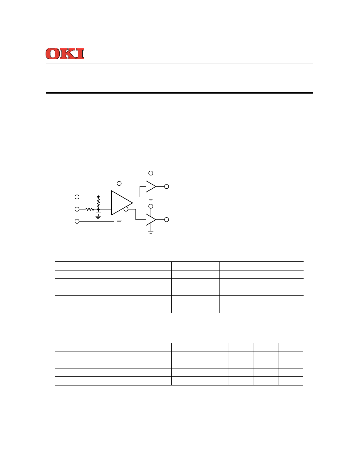
DESCRIPTION
KGA4217L, limiting Amplifier IC with 0.18 µm gate length GaAs MESFETs, has been designed for 10 Gb/s
digital communication systems. By using DCFL(Direct C
oupled FET Logic), high speed operation of 10 Gb/s
and low power dissipation have been realized. Capacitive coupling is recommended for I/O connections.
FUNCTION DIAGRAM
V
DD
V
DIN
DR1
DR2
5Ω
50Ω
DD
Q
V
DD
QN
DIN: Data Input
DR1: RF Bypass for data threshold stability
DR2: Data Threshold Control (Duty Cycle Control)
Q, QN: Complimentary Data Outputs
: Power Supply
V
DD
ABSOLUTE MAXIMUM RATINGS
Items Symbol Min. Max. Units
Supply Voltage V
Applied Voltage at DIN, DR1 VDI —0.3 1.5 V
Applied Voltage at DR2 VRI —2.5 2.5 V
Temperature at Package Base under Bias Ts —45 100 ¡C
Storage Temperature Tst —45 125 ¡C
DD
—0.3 2.3 V
ELECTRICAL CHARACTERISTICS
VDD = 2 V ±0.1 V, Ts = 0 to 70°C
Items Symbol Min. Typ. Max. Units
Maximum Operating Data Bit Rate DAR 10 Gb/s
Power Dissipation PW 0.25 0.35 W
Data Input Voltage Swing VI 0.035 0.6 Vpp
Data Output Voltage Swing VO 0.4 0.6 0.9 Vpp
GTD-18453 REV 1.0
5
)
)
)
)
5
5
4
5
5
)
5
0
G
N
1
Electronic Components KGA4217L
PAD LAYOUT
(—600 +25/0, 450 +0/—25)
(—495, 345)
(—495, 195)
(—495, 45)
(—495, —10
(—495, —255 )
GND
QN
GND
Q
(—405, —19
GND
(—245, 345
(—280, 255
(—405, 105
(—405, —4
(—280, —34
VDD
(—155, 255
(—245, —25
DR2
(—155, —3
Y
(0, 0)
X Y
(255, 345)
(345, 255)
X
(380, 345)
VDD
(405, 255)
(405, 95)
(405, —30)
(405, —255
Unit: µm
(495, 345)
GND
(495, 130)
DIN
(495, 5)
GND
(495, —22
DR1
(495, —34
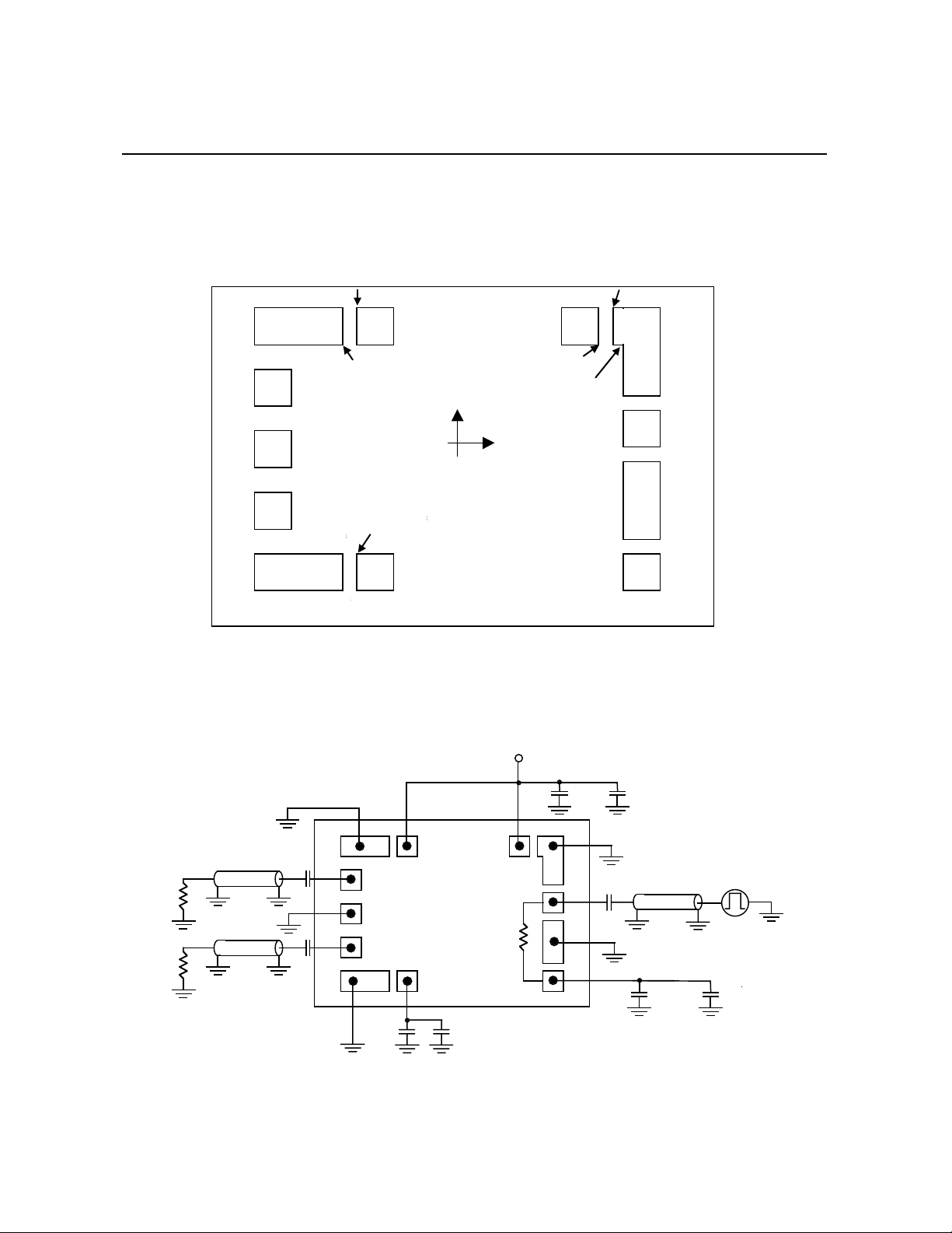
CONNECTION EXAMPLE
Z0=50Ω
50Ω
Z0=50Ω
50Ω
0.1µF
0.1µF
GND
QN
ND
Q
GND
220pF
VDD
DR2
0.1µF
50Ω
2.0V
VDD
GND
DIN
GND
DR1
0.1µF
(600 +0/—25, —450 +25/0)
0.1µF220pF
Z0=50Ω
220pF 0.1µF
OTE
- Capacitive coupling is recommended for high speed I/O terminals ( DIN, Q, QN).
- DR1 is RF bypass terminal for data threshold level stability and should be connected to
ground through RF bypass capacitors (220pF and 0.1 µF). The data threshold level is fixed by

GTD-18453 REV 1.0
1
Electronic Components KGA4217L
TYPICAL CHARACTERISTICS
Sensitivity vs. Data Bit Rate
Measurement condition : PRBS 231-1, BER=10
14
12
10
8
6
4
2
VDD=1.8V
VDD=2.0V
VDD=2.2V
Output Waveforms
-9
Measurement condition : DAR=10Gb/s,
31
PRBS 2
-1, VDD=2V, PW=250mW
VI=10 mVp-p
Minimum Input Voltage Swing [mVp-p]
0
2 4 6 8 10 12 14
Input Data Bit Rate [Gb/s]
Output Voltage Swing vs. Input Voltage Swing
700
600
500
400
300
200
Measurement condition : PRBS 231-1, BER=10
-9
VI=35 mVp-p
VI=600 mVp-p
Vert.: 120 mV/div, Horiz.: 25 ps/div
100
Output Voltage Swing ( mVp-p )
0
1 10 100 1000
Input Voltage Swing ( mVp-p )

GTD-18453 REV 1.0
l
)
1
Electronic Components KGA4217L
Duty Cycle vs. Data Threshold Contro
60
Input Voltage Swing
55
50
Duty Cycle [%]
45
40
0 0.2 0.4 0.6 0.8 1.0
Data Threshold Control Voltage V
35 mVp-p
m
-
DR2 [V]
Input Stage of KGA4217L
Sign Wave
DIN
DR1
DR2
IC Boundary
VDR2
EXAMPLE OF DIE MOUNTING
GND
QN
GND
Q
GND
VDD
GND
KGA
4217L
DR1
DR2
Cabity Floor ( Ground )
Bonding Wire ( Au : 30 micron
Micro-chipcapacitor ( 220pF )
50 ohm Transmission Line ( for DIN, Q,QN
n
n
DIN
GND
φ )

GTD-18453 REV 1.0
1
Electronic Components KGA4217L
 Loading...