

Page 1

Electronic Components
October 1, 2008
ODHKGA4163-02
KGA4163
10 Gbps Transimpedance Amplifier IC
GENERAL DESCRIPTION
Oki’s 10Gbps transimpedance amplifier is fabricated 0.1 m gate length P-HEMTs for high-speed optical
communication. The IC has high sensitivity and overload performance.
FEATURES
Transimpedance : 1.4kOhm (Differential)
Sensitvity : -20.5dBm
Overload : +2dBm
Chip Size : 0.80×1.09mm2
+3.3V Single Power Supply
ABSOLUTE MAXIMUM RATINGS (Ta = 25°C)
Parameters Symbol Units Rating
Supply Voltage V
Input Current I(IN) mA +4
Storage Temperature Range TST °C –40 to +125
RECOMMENDED OPERATING CONDITIONS
Parameters Symbol Units Min. Typ. Max.
Supply Voltage Vd V +3.05 +3.30 +3.55
Operating Temperature Range *1)
*1) At backside of die.
Ts °C -10 — +90
V 0 to +4
d
1/8
Page 2

ODHKGA4163-02
KGA4163
ELECTRICAL CHARACTERISTICS
(Ta= 25°C, Vd= +3.30V, C(diode) 0.15pF, unless otherwise noted )
Parameters Units Min. Typ. Max.
Transimpedance (Differential Output, I
Transimpedance (Single Ended Output, I
Maximum Single Ended Output Swing mVpp 300 450 570
Small Signal Bandwidth (–3 dB) GHz 9.0 11.0 —
Optical Sensitivity *1)
Optical Overload *1)
Output Return Loss ( f < 10 GHz ) dB — — -10
Input Bias Voltage (I
= 0 mA) *2), *3)
(IN)
Supply Current *2)
Power Consumption *2)
*1) Measured at 10
ratio of transmitter of 13dB.
*2) Under the recommended operating conditions (-10°C < Ta < 90°C, 3.05V < Vd < 3.55V)
*3) The input bias voltage will increase in the value, according to the input current. At I
1.0V.
-12
BER with a 231-1 PRBS at 10Gbps, assuming responsivity of photo diode of 1.0 A/W and extinction
<50 µA) 750 1400 1900
(IN)
<50 µA)
(IN)
375 700 950
dBm — -20.5 -19.8
dBm +1.0 +2.0 —
V +0.58 +0.75 +0.92
mA — 64 79
W — 0.20 0.28
= 2.5mA, the value is about
(IN)
2/8
Page 3
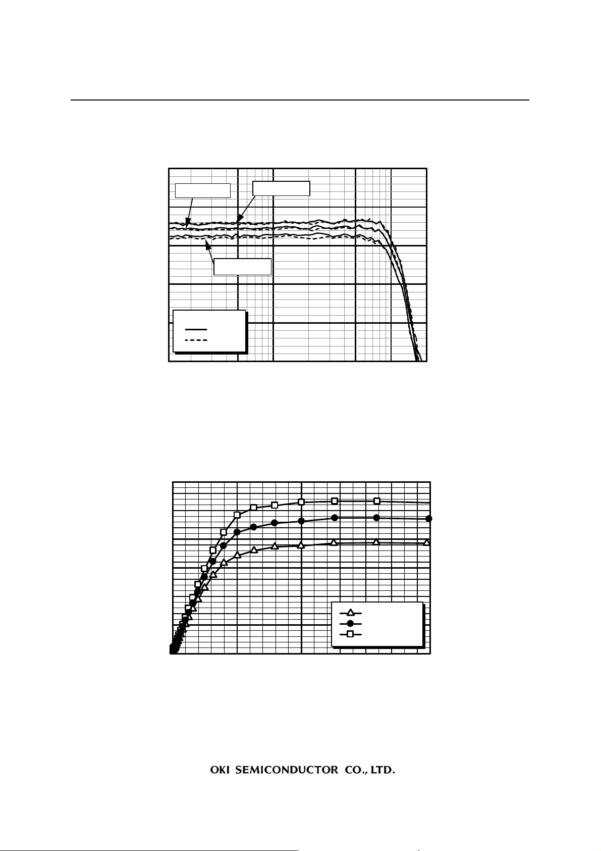
FREQUENCY RESPONSE (TYP.)
(Ta= 25°C, C(diode) 0.15 pF)
65
ODHKGA4163-02
KGA4163
Vd = 3.30V
Vd = 3.55V
60
55
Vd = 3.05V
50
Pin = -20dBm
45
OUTP
OUTN
Transim pedance [ dB]
40
0.13 20
0.5 1 5 10
Frequency [GHz]
OUTPUT VOLTAGE VS. INPUT CURRENT (TYP.)
(Ta= 25°C, Extinction ratio of optical input signal: 13dB)
600
500
400
300
200
Vd=3.05 V
100
Vd=3.30 V
Vd=3.55 V
Output Amplitude [mVpp]
0
0 0.5 1.0 1.5 2.0
Inpu t DC Current [mA]
3/8
Page 4

EYE DIAGRAMS (TYP.)
(Ta= 25°C, Optical Input Signal: PRBS 231-1 at 10Gbps, Extinction ratio of optical input signal: 13dB)
Vd = +3.05V
OUTP
OUTP
OUTP
OUTP
X:20ps/div,Y:100mV/div
OUTP
Input –21dBm
X:20ps/div,Y:5mV/div
Input –15dBm
X:20ps/div,Y:10mV/div
Input –10dBm
X:20ps/div,Y:50mV/div
Input -5dBm
Input -3dBm
Vd = +3.30V
OUTP
OUTP
X:20ps/div,Y:10mV/div
OUTP
X:20ps/div,Y:50mV/div
OUTP
X:20ps/div,Y:100mV/div
OUTP
Input –21dBm
X:20ps/div,Y:5mV/div
Input –15dBm
Input –10dBm
Input –5dBm
Input –3dBm
ODHKGA4163-02
Vd = +3.55V
OUTP
OUTP
X:20ps/div,Y:10mV/div
OUTP
X:20ps/div,Y:50mV/div
OUTP
X:20ps/div,Y:100mV/div
OUTP
Input –21dBm
X:20ps/div,Y:5mV/div
Input –15dBm
Input –10dBm
Input –5dBm
Input –3dBm
KGA4163
X:20ps/div,Y:100mV/div
OUTP
X:20ps/div,Y:100mV/div
X:20ps/div,Y:100mV/div
Input -1dBm
Input +1dBm OUTP
X:20ps/div,Y:100mV/div
OUTP
X:20ps/div,Y:100mV/div
X:20ps/div,Y:100mV/div
Input -1dBm
Input +1dBm OUTP
X:20ps/div,Y:100mV/div
OUTP
X:20ps/div,Y:100mV/div
X:20ps/div,Y:100mV/div
Input -1dBm
Input +1dBm OUTP
4/8
Page 5

BIT ERROR RATE CHARACTERISTICS (TYP.)
(Ta= 25°C, C(diode) 0.15pF, Extinction ratio of optical input signal: 13dB)
-3
10
10Gbps
PRBS:231-1
= 1 A/W
PD
ODHKGA4163-02
KGA4163
10
10
10
Bit Error Rate
10
10
10
10
-4
-5
-6
-7
-8
-9
-10
Vd=3.05V
Vd=3.30V
Vd=3.55V
-11
10
-12
10
-26 -24 -22 -20
+1 +2 +3 +4 +5
Optical Input Power [dBm]
5/8
Page 6

GROUP DELAY (TYP.)
(Ta= 25°C, Vd= +3.3V, C(diode) 0.15 pF)
OUTP
40
30
20
10
0
-10
ODHKGA4163-02
KGA4163
Pin = +1 dBm
Pin = 0 dBm
Pin = -1 dBm
Pin = -2 dBm
PAD LAYOUT
Group Delay [ps]
-20
Pin = -20 ~ -3 dBm
-30
-40
0 5 10 15 20
Frequency [GHz ]
Vd1
Vd2
GND1
OutP
GND2
In
GND1
CapGND2
All dimensions are in mm. Die thickness is 0.22mm(typ.)
Vth
GND2
GND2
OutN
6/8
Page 7

Vd
BLOCK DIAGRAM AND APPLICATION OUTLINES
0.1µF
220pF
V(PD)
ODHKGA4163-02
KGA4163
Photo
Diode
KGA4163
Vd1
Vd2
OUTP
Blocking
Capacitor
IN
OUTN
OP Amp.
6pF
50kohm
-
50kohm
+
6pF
Vth
GND2
Output Offset
Adjustment Circuit
GND1
Cap
150kohm
20pF
2200pF
GND1, GND2: Ground.
Vd1, Vd2: Power supply.
IN: Input; Connect to photo detector anode.
OUTP: Positive output.
OUTN: Negative output.
Cap: Pad for external capacitor to ground; The low frequency cutoff is reduced by
adding external capacitors. KGA4163 has on-chip 150k resistors with shunt
20pF capacitors to ground. With 2200pF external capacitors, the low frequency
cutoff will be about 30kHz.
Vth: Pad for output offset adjustment. This pad can be left floating;
[If use this function] Before using this pad, please refer the additional
information.
ASSEMBLY AND ESD CONSIDERATION
The product has air-bridge structures on the die surface. Do not use a vac uum tool to pick-up the product
and do not touch the product surface, in order not to damage to the air-bridges.
The product is recommended to be used in a hermetic environment, because the humidity stress test is not
performed. In a non-hermetic environment, the long term reliability is not guaranteed.
The product can be damaged by ESD. Therefore appropriate precautions must be taken to avoid exposure
to ESD and EOS during handling, assembly and testing of the product.
7/8
Page 8

ODHKGA4163-02
KGA4163
SAFETY AND HANDLING INFORMATION ON GaAs DEVICES
Arsenic Compound (GaAs Devices)
The product contains arsenic (As) as a compound.
This material is stable for normal use, however, its dust or vapor may be potentially hazardous to the
human body.
Avoid ingestion, fracture, burning or chemical treatment to the product.
• Do not put the product in your mouth.
• Do not burn or destroy the product.
• Do not perform chemical treatment for the product.
Keep laws and ordinances related to the disposal of the products.
NOTICE
1. The information contained herein can change without notice o wing to product and/or technical
improvements. Before using the product, please make sure that the infor mation being referred to is
up-to-date.
2. The outline of action and examples for application circuits describ ed herein have been chosen as an
explanation for the standard action and performance of the product. W hen planning to use the product,
please ensure that the external conditions are reflected in the actual circuit, assembly, and program designs.
3. When designing your product, please use our product below the specified maximum ratings and within the
specified operating ranges including, but not limit ed to, operating voltage, power dissipation, and operating
temperature.
4. OKI SEMICONDUCTOR assumes no responsibility or liability whatsoever for any failure or unusual or
unexpected operation resulting from misuse, neglect, improper installation, repair, alteration or accident,
improper handling, or unusual physical or electrical stress including, but not limited to, exposure to
parameters beyond the specified maximum ratings or operation outside the specified operating range.
5. Neither indemnity against nor license of a third party’s industrial and intellectual property right, etc. is
granted by us in connection with the use of the product and/or the information and drawings contained
herein. No responsibility is assu med by us for any infringement of a third party’s right which may result
from the use thereof.
6. The products listed in this document are intended for use in general electronics equipment for commercial
applications (e.g., office automation, communication equipment, measurement equipment, consumer
electronics, etc.). These products are not authorized for use in any system or application that requires
special or enhanced quality and reliab ility characteristics nor in any system or application where the failure
of such system or application may result in the loss or damage of property, or death or injury to humans.
Such applications include, but are not limited to, traffi c and automotive equipment, safety devices,
aerospace equipment, nuclear power control, medical equipment, and life-support systems.
7. Certain products in this document may need government approval before they can be exported to particular
countries. The purchaser assumes the responsibility of determining the legality of export of these products
and will take appropriate and necessary steps at their own expense for these.
8. No part of the contents contained herein may be reprinted or reproduced without our prior permission.
Copyright 2008 OKI SEMICONDUCTOR CO., LTD.
8/8
 Loading...