


UM10741
Fm+ development kit OM13320
Rev. 1 — 1 April 2014 User manual
Document information
Info Content
Keywords I2C-bus, Fm+, development tool, PCA9672, PCA9955
Abstract User manual for the Fm+ development board (OM13260) kit (OM13320).

NXP Semiconductors
UM10741
Fm+ development kit OM13320
Revision history
Rev Date Description
1.0 20140401 User manual; initial release
Contact information
For more information, please visit: http://www.nxp.com
For sales office addresses, please send an email to: salesaddresses@nxp.com
UM10741 All information provided in this document is subject to legal disclaimers. © NXP B.V. 2014. All rights reserved.
User manual Rev. 1 — 1 April 2014 2 of 61

NXP Semiconductors
1. Introduction
UM10741
Fm+ development kit OM13320
The Fm+ Development Kit (OM13320) is intended for several different tasks: from a
hands-on introduction, understanding, and use of the I
bus), to I
shows and sales pitches).
The kit has a core Printed-Circuit Board (PCB) assembly, and three add-on PCBs. Other
PCBs are available for advanced use or to support newly-released I
as they are introduced to the market.
The Fm+ Development Kit (OM13320) is supported by a Graphics User Interface (GUI)
software program that runs on a Pe rsonal Com pute r ( PC) u nder the Microso ft Windows 7
Operation System. In some uses the GUI is not required, and the Fm+ Development Kit
(OM13320) can be run as a standalone demonstration, requiring only an external power
adapter (not included).
2. Key features
I2C-bus masters
2
2
C device evaluation, and as a simple product demonstration platfo rm (for trade
Self-contained PCB with two independent I
2
Bus 1: On-card I
C MCU master (NXP LPC1343)
2
C buses
C-bus (Inter-Integrated Circuit
2
C-bus components
Bus 2: NXP LPC Xpresso MCU module (not included), and NXP PCA9665 bus
controller
USB interface to on-card MCU (for connection to a PC running the GUI software)
2
C-bus slaves
I
General Purpose Input/Output (GPIO): PCA9672 (one each on Bus1 and Bus2)
LED driver, with 16 constant current outputs: PCA9955 (with four RGB and four White
LEDs on Bus1)
Accessory sockets
Connectors for up to four daughter cards, each providing power, Bus1 and Bus2 I
2
signals
Connector for the Bus Buffer Board OM13398 (supplied) containing two PCA9617A bus
buffers
2
Connector for a third-party I
C-bus logger or I2C-bus controller (Beagle and Aardvark,
from Total Phase)
2
C buses
I
2
C-bus voltage: jumper select 5 V (external) or 3.3 V (on-card 3.3 V regulator)
I
2
C-bus pull-up resistors: jumper select of ‘high’, ‘med’ or ‘low’ loading
I
C
UM10741 All information provided in this document is subject to legal disclaimers. © NXP B.V. 2014. All rights reserved.
User manual Rev. 1 — 1 April 2014 3 of 61

NXP Semiconductors
Other features
SPI ports: One for on-card MCU, two more for LPC Xpresso
Serial Com Port: EIA232 with voltage level shifter and con nection to the LPC Xpresso
LED blinker: NXP PCA9901 one-wire with on-card LED
INT (Interrupt) and RST (Reset) Bus signal monitor LEDs (buffered)
Logic probe: Utility LEDs (buffered) to monitor signals by user jumper wire connection
External DC input (6 V DC maximum)
Prototype area: Uncommitted 8 × 8 100 mil pitch tie points for end user component
attachment
Test points and ground: for probe attachment to major signals
2
Connection of both I
C buses together (supplied 2-wire jumper)
3. Fm+ development kit quick tour
3.1 Kit contents
UM10741
Fm+ development kit OM13320
Before using the kit for the first time, please familiarize yourself with the various
components listed in Table 1
. See Figure 1.
Remark: Each PCB assembly is shipped in an anti-static bag. After the first use, these
may be discarded to simplify future storage.
a. Top layer b. Bottom layer
Fig 1. Fm+ development kit
UM10741 All information provided in this document is subject to legal disclaimers. © NXP B.V. 2014. All rights reserved.
User manual Rev. 1 — 1 April 2014 4 of 61

NXP Semiconductors
Table 1. Fm+ development kit contents
Components
Fm+ development board (OM13260)
GPIO target board (OM13303)
PCA9617A bus buffer demo board (OM13398)
Bridge board (OM13399)
Cable, USB Type A to Type B
Ribbon cable, 10 position (bag of two)
Jumper wires with female terminals (bag of ten)
Shorting jumpers (bag of twenty)
Hardware (bag of M3 screws and standoffs)
3.1.1 Box contents
The Fm+ Development Kit (OM13320) contains four PCB assemblies, cables, and loose
hardware. These should be retained in the box for future access. Depending upon the
desired use, some of the PCB assemblies may be attached to each other, either by plug
connection or by ‘stacking’ the GPIO PCB assemblies above the Fm+ Development
Board (OM13260), using the supplied ribbon cables and hardware.
UM10741
Fm+ development kit OM13320
UM10741 All information provided in this document is subject to legal disclaimers. © NXP B.V. 2014. All rights reserved.
User manual Rev. 1 — 1 April 2014 5 of 61

NXP Semiconductors
3.2 Supplied PCB assemblies
There are four PCB assemblies in the kit. Each has a spe cific function an d n ot all of th em
are used at the same time.
3.2.1 Fm+ Development Board (OM13260)
The large PCB, Figure 2, contains two separate I2C-bus structures, together with
supporting circuitry . Each bus has a bus master, one or more bus slaves, and user options
to change the bus voltage and bus pull-up resistors. Adjusting these changes the
operation of the buses to suit various goals. In addition, the two buses may be linked
together to operate a one I
(supplied) or the Bus Buffer Board OM133998 (supplied). See figure 3.5. Four identical
ports provide access for add-on boards that cont ain additional I
UM10741
Fm+ development kit OM13320
2
C-bus structure. This can be done with a two-wire jumper
2
C-bus devices.
Fig 2. OM13260 Fm+ development board PCB assembly
UM10741 All information provided in this document is subject to legal disclaimers. © NXP B.V. 2014. All rights reserved.
User manual Rev. 1 — 1 April 2014 6 of 61

NXP Semiconductors
3.2.2 GPIO target board (OM13303)
Outputs from the GPIO devices on the Fm+ Development Board (OM13260), and those
when using GPIO daughter cards (not supplied in the kit), require the GPIO Target Board
(OM13303). Each one has eight channels of LED indicator and push-button switches for
user input. See Figure 3
Fig 3. OM13303 GPIO target board PCB assembly
3.2.3 PCA9617A bus buffer demo board (OM13398)
Bus buffers bridge two I2C-bus segments, which are provided on the Fm+ Development
Board (OM13260) by Bus1 and Bus2. Bus buffer daughter ca rd s, such as th e PCA9 617 A
Bus Buffer Demo Board (OM13398) (supplied in the kit) can be installed directly on Port E
(CN12). See Figure 4
UM10741
Fm+ development kit OM13320
.
.
Fig 4. OM13260 bus buffer PCB assembly
UM10741 All information provided in this document is subject to legal disclaimers. © NXP B.V. 2014. All rights reserved.
User manual Rev. 1 — 1 April 2014 7 of 61

NXP Semiconductors
3.2.4 Bridge board (OM13398)
Some existing Demo Boards used a single row connector with nine pins. To use these
with the Fm+ Development Kit requires the Bridge Board (OM13399, supplied in the kit).
See Figure 5
UM10741
Fm+ development kit OM13320
.
Fig 5. OM13399 bridge board PCB assembly
3.2.5 Daughter cards (not supplied in the kit)
These are not in the OM13230 kit, and should be obtained separately. Daughter cards
hedge against obsolescence so that the Fm+ Development Kit (OM13320) can be used
with future devices by adding newly released daughter cards as they become available.
An example daughter card is shown in Figure 6
Fig 6. Example daughter card PCB assembly
.
UM10741 All information provided in this document is subject to legal disclaimers. © NXP B.V. 2014. All rights reserved.
User manual Rev. 1 — 1 April 2014 8 of 61

NXP Semiconductors
Fm+ development kit OM13320
4. First time setup: Fm+ development board kit (OM13320)
4.1 Before you begin
To use the Fm+ Development Kit (OM13320) for the first time requires some hardware
setup and installation of both firmware (on the Fm+ Developmen t Board OM13260) and
software on the attached computer.
The following three steps must be completed:
UM10741
1. Install Jumpers on the Fm+ Development Board (OM13260) (see Section 4.3
2. Install Firmware on the Fm+ Development Board (OM13260) (see Section 4 .6
3. Install the NXP GUI Software on the computer to be used with the kit
(see Section 4.7
).
4.2 First time setup of the Fm+ development board (OM13260)
Several jumpers must be installed before using the Fm+ Develop ment Board (OM13260)
PCB. The on-board microcontroller (MCU) must contain the appropriate firmware.
To install the firmware requires the connection to a Personal Computer (PC) running
Microsoft Windows 7/64 Operating System and a USB port.
4.3 OM132680 jumpers
The jumpers and their function are shown in Table 2. Using Figure 7 and the table data,
install the jumpers.
Table 2. OM13260 jumpers
Jumper Label Function First time
JP1 XPRESSO POWER Close
JP2 HDD Open
JP3 CONNECT Close
JP4 RST Open
JP5 PCA9955 address GND
JP6 ISP Open
JP7 SPI SEL 1
JP10 PCA9672 address GND
JP11 SDA1 pull-up A
JP12 SCL1 pull-up A
JP13 Bus1 bus voltage 3V3
JP20 PCA9672 address GND
JP21 SDA2 pull-up A
JP22 SCL2 pull-up A
JP23 Bus2 bus voltage 3V3
).
).
UM10741 All information provided in this document is subject to legal disclaimers. © NXP B.V. 2014. All rights reserved.
User manual Rev. 1 — 1 April 2014 9 of 61

NXP Semiconductors
UM10741
Fm+ development kit OM13320
Fig 7. OM13260 test point locations
4.4 OM13260 Port E bypass
Depending up the intended operation of the Fm+ Development Board (OM1326 0),
Port E (CN12) should be left open, or linked with a jumper wire, or for the attachm ent of a
Bus Buffer Board. The PCA9617A Bus Buf fer Demo Board (OM13398) is supplied in the
kit.
For the purpose of this quick setup section, install the two-wire jumper (supplied) as
shown in Figure 8
Remark: The two-wire jumper requires a twist, as shown. The diagonally opposite pins
are linked.
.
UM10741 All information provided in this document is subject to legal disclaimers. © NXP B.V. 2014. All rights reserved.
User manual Rev. 1 — 1 April 2014 10 of 61

NXP Semiconductors
Fig 8. OM13260 Port E jumper
4.5 OM13260 mounting hardware
To prevent damage to the table surface, it is recommended that met a l hardware (supplied
in the kit) is installed in the four mounting holes. This raises the PCB assembly about
6mm. See Figure 9
UM10741
Fm+ development kit OM13320
.
Fig 9. OM13260 mounting hardware
Remark: Save the completed Fm+ Development Board, now install the NXP USB Driver.
UM10741 All information provided in this document is subject to legal disclaimers. © NXP B.V. 2014. All rights reserved.
User manual Rev. 1 — 1 April 2014 11 of 61

NXP Semiconductors
4.6 NXP firmware installation
The micro on the Fm+ Development Board needs firmware running on it to interface with
the GUI running on a Windows 7 PC over USB. The board is shipped with a blank
microprocessor, so user action is necessary for proper operation.
UM10741
Fm+ development kit OM13320
An installation user manual UM10785 (Ref. 1
the process. A quick overview is presented here.
1. Download NXP_Fm+_Eval_Board_V1_0_firmware.zip from
www.nxp.com/demoboard/OM13320.html#documentation
2. Connect a USB cable from the PC USB port to CN5.
3. Install the Connect (JP3) jumper to connect the USB communications.
4. Install the ISP (JP6) jumper to put the MCU into In-System Programming mode.
5. Install and then remove RST (JP4) jumper to reset the MCU.
6. The MCU will enumerate on the PC as a disk drive called CRP_DISABLD.
7. Delete the file on the MCU (size may vary — up to 32 kB).
8. Copy the new firmware file NXP_Fm_Eval_Board_V1_0.bin, extracted from the
zip file to the MCU.
9. Remove the ISP (JP6) jumper.
10. Install and then remove RST (JP4) jumper to reset the MCU.
) is available at for a complete explanation of
4.7 NXP GUI installat ion
A Graphical User Interface (GUI) is provided which allows easy manipulation of the
devices included on the Fm+ Development Board and ma ny others that can be connected
to the board via daughter cards.
An installation user manual UM10785 (Ref. 1
the process. A quick overview is presented here.
1. Download NXP_Fm_Board_V1_0_Installation.zip from
www.nxp.com/demoboard/OM13320.html#documentation
2. Extract NXP Fm+ Board V1.0 Installation.exe and run.
3. Follow the instruction prompts. Select the default answers.
This GUI uses a USB Human Interface Driver (HID), so no driver installation is required.
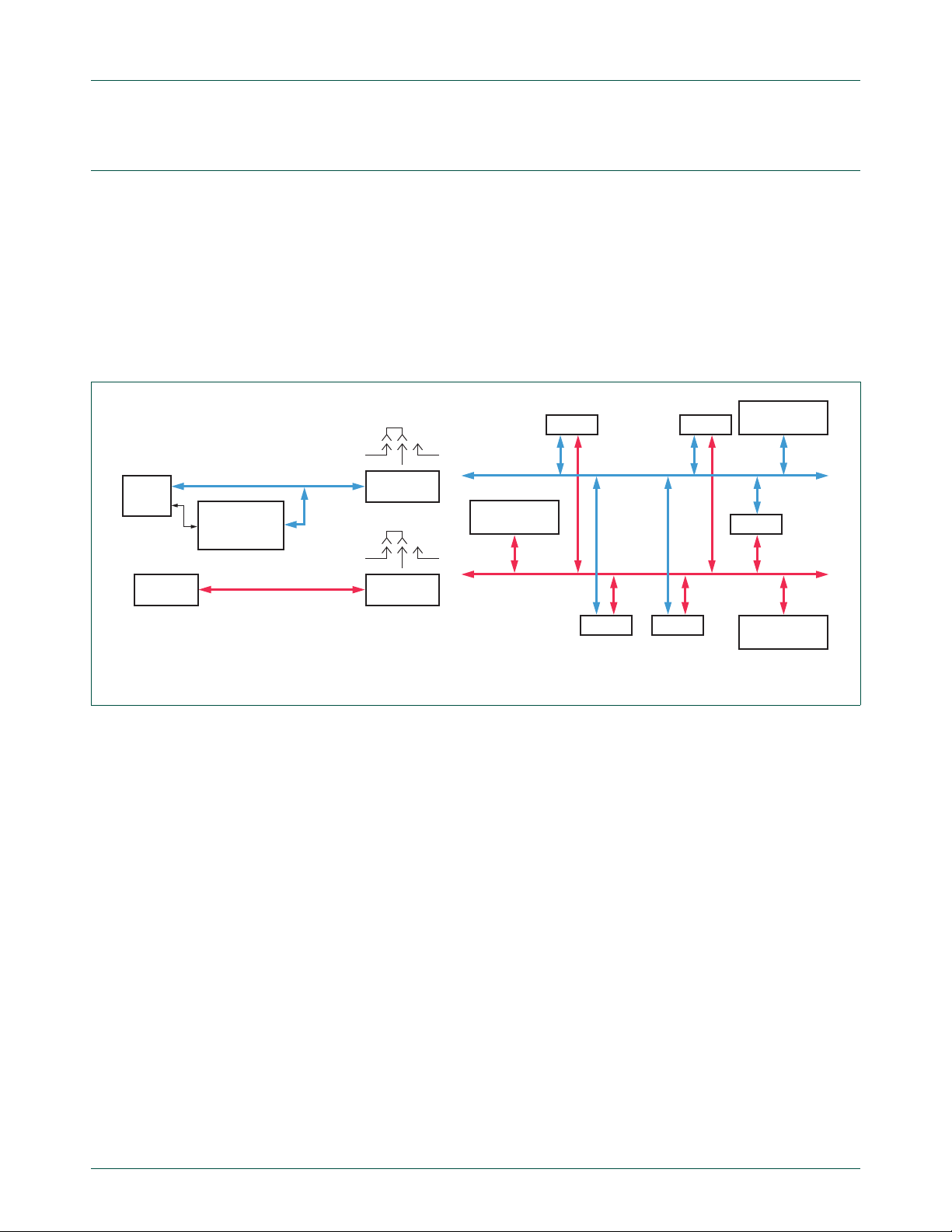
If the firmware and GUI installs are successful, an Fm+ Development Board block
diagram is displayed when the GUI executes (Figure 10
UM10741 All information provided in this document is subject to legal disclaimers. © NXP B.V. 2014. All rights reserved.
User manual Rev. 1 — 1 April 2014 12 of 61
) is available for a complete explanation of
).
NXP Semiconductors
aaa-012039
PCA9672
8-channel GPIO
Port B
Port E
Port A
PCA9672
8-channel GPIO
I2C-bus 1
I
2
C-bus 2
5 V
5 V
Port C
Port D
PCA9955
16-channel LED
3.3 V
PULL-UP
RESISTORS
3.3 V
PULL-UP
RESISTORS
I2C-bus 1
PCA9665
BUS
CONTROLLER
LPC1343
MCU
I
2
C-bus 2
parallel port
LPC
XPresso
5. Fm+ development board (OM13260)
The Fm+ Development Board (OM13260) PCB assembly is self- contained, requiring only
DC power to operate. Depending upon the firmware installed on the Fm+ Development
Board (OM13260), it can also operate with a connected Personal Computer (PC) via a
USB cable.
The modular design of the kit and this board in par ticular allows accessory boards to be
easily connected.
5.1 Theory of operation
UM10741
Fm+ development kit OM13320
Fig 10. Fm+ development board bus structure
An I2C-bus requires a Master and one or more Slaves. The two bus signals, clock SCL
and data SDA, are wired-OR and require pull-ups to a DC power supply. Two similar but
separate I
2
C buses each support one Master and at least one Slave device on the bo ard .
The two buses may be linked by either a Bus Buffer Board (OM13398 supplied in the kit)
or a wire jumper, at the Port E connector (CN12).
The signals from both buses are available simultaneously at each of four connectors,
Port A through Port D (CN1 through CN4, respectively). These are intended for
2
attachment of accessory daughter cards, which will be made available as future I
C-bus
devices are released.
The size of the pull-up resistors can be changed by moving shorting jumpers (JP1, JP2,
JP1 1, and JP12), providing selection of ‘Low’ ‘Med’ and ‘High’ resistor values scaled to the
2
C-bus drive strength. When both buses are joine d by a jump er wire, the pull- ups
Fm+ I
are effectively in parallel, and have one-half the stated resistance values.
UM10741 All information provided in this document is subject to legal disclaimers. © NXP B.V. 2014. All rights reserved.
User manual Rev. 1 — 1 April 2014 13 of 61
Operating voltage of the I
that select either 3.3 V or 5 V connected to the pull-up resistors. Compliant I
devices can tolerate 5.5 V (maximum), regardless of the device operating voltage.
2
C-bus depends upon the shorting jumpers (JP13 and JP23)
2
C-bus

NXP Semiconductors
Each bus has a GPIO 8-bit Slave device (PCA9672, IC10 an d IC2 0), an d Bus 1 also has
an LED Driver 16-channel device (PCA9955, IC6). All sixteen outputs are connected to
LEDs, for visual indication. The 8-bit GPIOs require connection of GPIO Target Boards
(OM13303, supplied in the kit) to both indicate the output using eight LEDs and a llow user
input from eight push switches.
An NXP LPC1343 Microcontroller (MCU) serves as both the Bus 1 Master, and the USB
link. The firmware on the MCU can be replaced by the In-System Programming (ISP)
mode, with data sent over the USB link (CN5).
Bus 2 has a Parallel to I
an optional NXP LPC Xpresso module (not supplied). That module is also an I
and connected to Bus 2.
Remark: Although Bus 2 has more than one I
The remaining circuitry is to support the I
PC over a USB link.
UM10741
Fm+ development kit OM13320
2
C-bus Controller device (PCA9665, IC6), which is to be driven by
2
C Master, only one is active at any time.
2
C devices, and provide communications with the
2
C Master
The main operating voltage on th e Fm+ Development Boa rd (OM13260) is 3.3 V supplied
2
from a linear regulator (IC1). Some circuits and the op tional I
C-bus pull-ups may run from
5 V derived either from the USB host (typically a PC) or an AC-DC power supply (not
supplied in the kit). The actual voltage is seldom 5 V, due to cable losses, plus an
additional drop in a series connected diode used to OR the two input s. Wh ichever has th e
highest voltage has priority.
A shunt Zener diode (6.2 V) protects the board from reverse polarity and overvoltage at
the DC Power connector (CN6).
To aid in understanding digital signal levels on the board, two ‘logic probe’ circuits are
provided. These are buffered LEDs (Green, D6 and Red, D7), which light if their
respective inputs (CN11) are grounded.
2
Two global digital signal nets, called INT (interrupt) and RST (reset) connect all I
C-bus
devices on the board and also the Port A – Port E Daughter Card connectors. These are
also connected to the Master (MCU, IC5) on Bus 1, the Master (Bus Controller, IC4), and
the LPC Xpresso module.
2
Remark: The I
only reset the I
The test points provide monitoring of interrup ts (usually generated by I
software reset of Fm+ class I
C global Reset is not the same as the MCU Reset. Resetting the MCU will
2
C-bus if the MCU firmware is intended to create a global reset.
2
2
C-bus devices that have that feature.
C-bus Slaves) and
Additional buffered LEDs are provided (D19, RST and D20, Interrupt) on the Fm+
Development Board (OM13260) for visual indication.
V arious MCU and LPC Xpresso signals are made a vailable through additional connectors.
These include a serial Port (CN7) with EIA232 volta ge level translation (I C2) and SPI Bus
signals (SP0, CN9 and SP1, CN8) from the LPC Xpresso module, together with SPI Bus
(SP2, CN16) from the MCU (IC5).
A prototyping area is provided for solder connection of components that may be required
by an application circuit beyond this board’s design. Power supplies and other sign als are
readily available.
UM10741 All information provided in this document is subject to legal disclaimers. © NXP B.V. 2014. All rights reserved.
User manual Rev. 1 — 1 April 2014 14 of 61

NXP Semiconductors
UM10741
Fm+ development kit OM13320
On the Fm+ Development Board (OM13260) V3.0 there is an LED Blinker device
(PCA9901, IC3) and LED indicator (D10), while not strictly an I
one-wire protocol, it belongs to the NXP I
Remark: The PCA9901 will be made obsolete, and will not be present on future versions
of the Fm+ Development Board (OM13260).
The operation of the Fm+ Development Board (OM13260) is greatly enhanced by
third-party tools (not supplied in the kit) that may be attached to either I
dedicated connectors (Bus1, CN17 and Bus2, CN18), labeled ‘TESTER’.
5.2 Circuit description
The schematic diagram has multiple sheets. For clarification, only fragments of the
schematic are shown here. The full schematic should be downloaded if required. The
following pages are divided in to several sections covering the powe r supply, USB
interface, Bus1, Bus2, and support circuits.
5.2.1 Power supply
The Fm+ Development Board (OM13260) operates from DC, either from the USB Host
connector (CN5) or an optional external AC-DC power adapter (not supplied in the kit) via
connector (CN6). See Figure 11
automatic, using ORing diodes (D1 and D2). The main power on the Fm+ Development
Board (OM13260) is 3.3 V from a linear regulator (IC1), but some of the circuits are
powered directly from the incoming supply, which is a nominal 5 V. Linear regulator (IC1)
uses the PCB bottom layer copper as a heat sink. The Fm+ Development Board
(OM13260) external DC input is protected against reverse polarity or overvoltage by
Zener diode (D3). Both input sources are scaled by resistor dividers (R1, R2 and R39,
R40) and fed to the MCU (IC5) Port1 ADC inputs for voltage leve l monitoring. The VBUS
from the USB Host is fed to the MCU Port 0 so that the MCU can detect that a USB
connection is available. Green LED (D4) confirms 5 V, and Green LED (D5) confirms
3.3 V.
2
2
C-bus product portfolio.
and Figure 12. Selection of the power source is
C device as it uses a
2
C-bus through
UM10741 All information provided in this document is subject to legal disclaimers. © NXP B.V. 2014. All rights reserved.
User manual Rev. 1 — 1 April 2014 15 of 61
NXP Semiconductors
aaa-011872
VBUS
R2
10 kΩ
R1
10 kΩ
USB_V
GND
R4
10 kΩ
R3
10 kΩ
MCU_VBUS
GND
D2
STPS2L40U
GND
C2
100 pF/10 V
+5V
R5
820 Ω
D4
LTST-C170KGKT GRN
+5 V
5
HS1
PCBPAD
67489
10
1
23
HS1
HS6
HS5
HS4
ADVTAB
HS3
HS2
IN OUT
GND
IC1
ZLDO1117G33TA
C1
100 pF/10 V
+3V3
R6
820 Ω
D5
LTST-C170KGKT GRN
+3.3 V
GND
3V3 REGULATOR
R40
20 kΩ
R390
10 kΩ
EXT_V
GND
D1
STPS2L40U
Max input 6.2 V DC
GNDGND
EXT POWER
D3
1SMB5920BT3
6V2
CN6
DD-JACK-GMT
UM10741
Fm+ development kit OM13320
Fig 11. Power supply
UM10741 All information provided in this document is subject to legal disclaimers. © NXP B.V. 2014. All rights reserved.
User manual Rev. 1 — 1 April 2014 16 of 61
Fig 12. Power supply and USB section
NXP Semiconductors
5.2.2 USB interface
The USB Host connector (CN5) provides DC power and USB connectivity using the MCU
(IC5) hardware interface, see Figure 12
resistors (R27 and R28) and protected by an ESD network (IC7). To signal to the host that
the USB connection is required, the USB signal DP is pulled to 3.3 V via a resistor (R18)
and a transistor (Q1). USB Connection is contro lled by the MCU (IC5) via signal CON_EN
and can be disabled by removing a jumper (JP3) ‘CONNECT’. Whe n the MCU requests a
USB connection, and the jumper (JP3) is installed, the green LED (D9) is ON. MCU
activity is displayed by the Heart Beat green LED (D8), which is set to blink at about
one per second.
UM10741
Fm+ development kit OM13320
and Figure 13. USB data lines are terminated by
+3V3
IC5G$8
USB_DP
USB_Dm
LPC134X_HVQFN32
14
13
Fig 13. USB interface
5.3 Bus one (Bus1)
R17
820 Ω
D9
10 kΩ
2.2 kΩ
SOFTCONNECT
VBUS
Q1
PDTA123YT
R18
1.5 kΩ
GND
DP
DM
VBUS
GND
GND
5
GND
6
CN5-3
CN5-2
CN5-1
CN5-4
LTST-C170KGKT GRN
R27
R28
33 Ω
33 Ω
GND
D8
CONFIG
USB_LED
CON_EN
IC7
2
IO1
1
GND
PRTR5V0U2X
R20
820 Ω
LTST-C170KGKT GRN
JP3-1
USB_CONNECT
3
IO2
4
VCC
CONNECT
JP3-2
USB PORTUSB INTERFACE
aaa-011873
There are two almost identical I2C buses on the Fm+ Development Board (OM13260),
called Bus1 and Bus2. These share a ground and power connection but may be operated
independently.
2
Remark: The bus voltage for each I
2
I
C-bus, 5 V for the other I2C-bus).
C may be different (for example 3.3 V for one
5.3.1 Bus1 master (MCU LPC1343)
Microcontroller (MCU) (LPC1343, IC5) serves as the Bus1 Master and the USB Bridge.
Firmware installed on the Fm+ Development Board (OM13260) is stored in non-volatile
memory, which has a limit of 32 kB. The MCU may be programmed through the USB por t
or the JTAG connector (CN 19), using Single Wire Debug (SWD), see Figure 14
Figure 15
UM10741 All information provided in this document is subject to legal disclaimers. © NXP B.V. 2014. All rights reserved.
User manual Rev. 1 — 1 April 2014 17 of 61
.
and
NXP Semiconductors
aaa-011874
R38
10 kΩ
JP4-1
LPC SWD PROG CONNECTOR
R37
100 kΩ
JP4-2
RST
GND
+3V3+3V3
GND
MCU_SCLK
SWDIO
SWD_RESET
CN19-10
CN19-9
CN19-8
CN19-7
CN19-6
CN19-5
CN19-4
CN19-3
CN19-2
CN19-1
During programming or at other times it may be necessary to reset the MCU, by briefly
shorting JP4 (see Figure 15
Remark: An MCU Reset is not the same as an I
affect the I
it is reset.
UM10741
Fm+ development kit OM13320
).
2
2
C-bus, unless the MCU firmware is designed to issue an I2C Bus Reset when
C Bus Reset. Resetting the MCU will not
Fig 14. MCU SWD interface
Fig 15. MCU SWD interface section
MCU Port0 and Port1 provide most of the signals used by the Fm+ Development Board
(OM13260), see Figure 16
and Figure 17. I2C Bus1 is connected to the MCU Port0 via
RC edge rate control networks that provide bus fall time control (SCL1: R42 and C18;
UM10741 All information provided in this document is subject to legal disclaimers. © NXP B.V. 2014. All rights reserved.
User manual Rev. 1 — 1 April 2014 18 of 61
SDA1: R43 and C17).
NXP Semiconductors
aaa-011876
LPC134X_HVQFN32
IC5G$2
22
23
24
25
26
30
31
32
7
12
20
27
EXT_V
USB_V
SWDIO
RESET
+3V3
R41
10 kΩ
GND
JP2-1
JP2-2
HDD
R/PIO1_0/ADC1/CT32B1_CAP0
R/PIO1_1/ADC2/CT32B1_MAT0
R/PIO1_2/ADC3/CT32B1_MAT1
SWDIO/PIO1_3/ADC4/CT32B1_MAT2
PIO1_4/ADC5/CT32B1_MAT3/WAKEUP
PIO1_5/UART_RTS/CT32B0_CAP0
PIO1_6/UART_RXD/CT32B0_MAT0
PIO1_7/UART_TXD/CT32B0_MAT1
PIO1_8/CT16B0_CAP0
PIO1_9/CT16B1_MAT0
PIO1_10/ADC6/CT16B1_MAT1
PIO1_11/ADC7
LPC134X_HVQFN32
IC5G$4
28
PIO3_2
LPC134X_HVQFN32
IC5G$3
1
PIO2_0/UART_DTR
UM10741
Fm+ development kit OM13320
+3V3
LPC134X_HVQFN32
PIO0_1/CLKOUT/CT32B0_MAT2/USB_TOGGLE
PIO0_2/SSP_SSEL/CT16B0_CAP0
PIO0_3/USB_VBUS
PIO0_6/USB_CONNECT/SCK
PIO0_8/SSP_MISO/CT16B0_MAT0
PIO0_9/SSP_MOSI/CT16B0_MAT1/SWD
SWCLK/PIO0_10/SSP_CLK/CT16B0_MAT2
R/PIO0_11/ADC0/CT32B0_MAT3
IC5G$1
Fig 16. IC5 MCU Port0
RESET/PIO0_0
PIO0_4/I2C_SCL
PIO0_5/I2C_SDA
PIO0_7/CTS
2
SWD_RESET
3
8
MCU_SSN
9
MCU_VBUS
10
SCL1A
11
SDA1A
15
CON_EN
16
USB_LED
17
MCU_MISO
18
MCU_MOSI
19
MCU_SCLK
21
INT
R43
100 Ω
R33
10 kΩ
GND
100 Ω
GND
ISP
R42
C17
10 pF
JP6-1
JP6-2
TF EDGE RATE CONTROL
GND
SCL1
SDA1
C18
10 pF
aaa-011875
UM10741 All information provided in this document is subject to legal disclaimers. © NXP B.V. 2014. All rights reserved.
User manual Rev. 1 — 1 April 2014 19 of 61
Fig 17. IC5 MCU Port1
The HVQN32 package has a thermal pad grou nd connection, and ope rates from the main
3.3 V supply. The MCU operates with a 12.00 MHz crystal controlled oscillator. The
frequency value and accuracy is necessary for correct USB timing (see Figure 18
).

NXP Semiconductors
LPC134X_HVQFN32
GND9
GND8
GND7
GND6
GND5
GND4
GND3
GND2
GND1
IC5G$7
UM10741
Fm+ development kit OM13320
LPC134X_HVQFN32
4
XTALIN
XTALOUT
41
40
39
38
37
36
35
34
33
GND
LPC134X_HVQFN32
VDDIO_EXT_1
VDDMAIN_EXT
IC5G$6
5
IC5G$5
15 pF
6
29
C8
GND
C9
100 nF
12 MHz
GND
XE1
NX5032GA
GND
+3V3
GND
aaa-011877
C7
15 pF
C6
100 nF
Fig 18. IC5 MCU Port1, oscillator and power supply
5.3.2 Bus1 pull-up resistors
The Bus1 is pulled up to either the 3.3 V or 5 V supplies via JP13. Three different value
pull-up resistors are provided by jumper selection, JP11 and JP12. The values of the
pull-up resistors are shown in Table 3
SDA signal lines. Bus2 has a similar arrangement. See Figure 19
+3V3
JP13-1
JP13-2
JP13-3
+5V
. Separate pull-ups are provided for the SCL and
and Figure 20.
1.1 kΩ
GND
R16
634 Ω
R15
324 Ω
R14
1.1 kΩ
R13
634 Ω
R12
324 Ω
R11
C10
100 nF
JP12-6
JP12-4
JP12-2
JP11-6
JP11-4
JP11-2
JP12-5
JP12-3
JP12-1
JP11-5
JP11-3
JP11-1
SCL1
SDA1
I2C BUS-1 PULL-UP RESISTOR NETWORK
aaa-011878
Fig 19. Bus1 pull-ups and bus voltage selector
UM10741 All information provided in this document is subject to legal disclaimers. © NXP B.V. 2014. All rights reserved.
User manual Rev. 1 — 1 April 2014 20 of 61

NXP Semiconductors
UM10741
Fm+ development kit OM13320
Fig 20. Bus1 pull-ups section
T able 3. Bus pull-up resistors
Strength Position Value Bus1 SCL Bus1 SDA Bus2 SCL Bus2 SDA
LOW A 1.1 kΩ R16 R13 R26 R23
MID B 634 Ω R15 R12 R25 R22
HIGH C 324 Ω R14 R11 R24 R21
5.3.3 LED driver slave (PCA9955)
Bus1 is also used to control the LED Driver (PCA9955, IC6). Th e LED Driver has constant
current outputs and is directly connected to the LEDs, without customary series resistors.
The LEDs are powered directly from the 5 V supply, thus avoiding further power
dissipation in the 3.3 V linear regulator, IC1. The sixteen channels drive eight LED
clusters consisting of four White LEDs (LED12 – LED15) and four RGB LED clusters
(LED0 – LED11). The maximum current available for each channel is set by R35 and the
variable resistor R36. The LEDs use the PCB top metal for heat dissipation, the LED
driver is in the HTSSOP28 package has a thermal pad ground connection, and operates
from the main 3.3 V supply. See Figure 21
and Figure 22.
UM10741 All information provided in this document is subject to legal disclaimers. © NXP B.V. 2014. All rights reserved.
User manual Rev. 1 — 1 April 2014 21 of 61

NXP Semiconductors
38
37
36
35
34
33
32
31
30
29
GND10
GND9
GND8
GND7
GND6
GND5
GND4
GND3
GND2
GND1
GND
IC6G$2
PCA9955PW
aaa-011879
GND
C5
22 pF/16 V
+3V3
R35
820 Ω
PCA9955 Address:
0xC0h or 0xD0h
GND
JP5-1
JP5-2
JP5-3
Iset
GND
R36
10 kΩ
GND
LED MAX BRT
1
2
3
4
5
6
7
8
9
10
REXT
A0
A1
A2
OE/A3
LED0
LED1
LED2
LED3
VSS
LED0
LED1
LED2
LED3
11
12
13
14
LED4
LED5
LED6
LED7
LED4
LED5
LED6
LED7
PCA9955PW
IC6G$1
LED[0..11]
PCA9955 16-ch CONSTANT
CURRENT LED DRIVER
VDD
SDA
SCL
RESET
VSS
LED15
LED14
LED13
LED12
VSS
LED11
LED10
LED9
LED8
28
27
26
25
24
23
22
21
20
19
18
17
16
15
GND
+3V3
SDA1
SCL1
RESET
LED15
LED14
LED13
LED12
LED11
LED10
LED9
LED8
GND
RGB LEDs
LED[12..15]
LED9
LED10
LED11
D14R
D14G
D14B
+5V
LED6
LED7
LED8
D13R
D13G
D13B
LED3
LED4
LED5
D12R
D12G
D12B
LED0
LED1
LED2
D11R
D11G
D11B
+5V
WHITE LEDs
LED15
D18
LED14
D17
LED13
D16
LED12
D15
+5V
UM10741
Fm+ development kit OM13320
Fig 21. Bus1 LED driver 16-channel
UM10741 All information provided in this document is subject to legal disclaimers. © NXP B.V. 2014. All rights reserved.
Operation of all sixteen LEDs at maximum current will overheat the LED driver, which is
protected by an internal thermal limiter. The device will shut down and recover when the
temperature has fallen.
When powered from the USB port (CN5) the USB Host is typically limited to 500 mA, and
it will shut down before the LEDs reach maximum current. Operation from an external DC
power supply connection (CN6) is required to drive the LEDs to the maximum current per
channel of 57 mA, for a total of approximately 1 A.
User manual Rev. 1 — 1 April 2014 22 of 61
Fig 22. Bus1 LED driv er 16-channel section

NXP Semiconductors
The recommended AC-DC adapter is Digikey PN: 62-1132-ND (not supplied).
See Figure 23
UM10741
Fm+ development kit OM13320
.
Fig 23. AC-DC adapter, 6 V, 2 A
The Slave address is set by JP5, summarized in Table 4.
Remark: The PCB is marked with hexadecimal (8-bit) address data, but data sheets and
the NXP GUI use the 7-bit address values. See Table 4
Table 4. LED driver address selection
JP5 connected to Hexad ecimal 8-bit address NXP 7-bit address
Address MSB LSB Address MSB LSB
GND 0xC0 1100 0000 0x60 110 0000
V
CC
0xD0 1101 0000 0x68 110 1000
5.3.4 GPIO slave (PCA9672)
The GPIO (PCA9672, IC10) is connected to Bus1, and provides eight input/output
channels at CN10. Jumper JP10 sets the device address to one of four options,
depending on whether the A0 pin is connected to GND, V
similar arrangement for a second GPIO (PCA9672, IC20). See Figure 24
Remark: The PCB is marked with hexadecimal (8-bit) address data, but data sheets and
the NXP GUI use the 7-bit address values. This is summarized in Table 5
.
, SCL, or SDA. Bus2 has a
CC
and Figure 25.
.
UM10741 All information provided in this document is subject to legal disclaimers. © NXP B.V. 2014. All rights reserved.
User manual Rev. 1 — 1 April 2014 23 of 61

NXP Semiconductors
UM10741
Fm+ development kit OM13320
+3V3
JP10-1
JP10-3
JP10-5
JP10-7
GND
SDA1
SCL1
JP10-2
JP10-4
JP10-6
JP10-8
Fig 24. Bus1 GPIO 8-bit
Table 5. LED driver address selection
A0 connected to He xadecimal 8-bit address NXP 7-bit addres s
GND 0x44 0100 0100 0x22 010 0010
V
SCL 0x54 0101 0100 0x2A 010 1010
SDA 0x56 0101 0110 0x2B 010 1011
PCA9672 addresses:
VDD = 0x46h
SDA1 = 0x56h
SCL1 = 0x54h
GND = 0x44h
CC
+3V3
SDA1
SCL1
INT
RESET
15
SDA
14
SCL
13
INT
3
RESET
2
A1
1
A0
IC10
PCA9672PW
+3V3
16
8
GND
VDD
GND
IO0
IO1
IO2
IO3
IO4
IO5
IO6
IO7
4
5
6
7
9
10
11
12
GPIO1_0
GPIO1_1
GPIO1_2
GPIO1_3
GPIO1_4
GPIO1_5
GPIO1_6
GPIO1_7
GPIO1_[0..7]
GPIO1_7
GPIO1_6
GPIO1_5
GPIO1_4
GPIO1_3
GPIO1_2
GPIO1_1
GPIO1_0
+3V3
GND
PCA9672 8-bit GPIO (Bus1)
Address MSB LSB Address MSB LSB
0x46 0100 0110 0x23 010 0011
CN10-10
CN10-9
CN10-8
CN10-7
CN10-6
CN10-5
CN10-4
CN10-3
CN10-2
CN10-1
aaa-012040
Fig 25. Bus1 GPIO 8-bit section
UM10741 All information provided in this document is subject to legal disclaimers. © NXP B.V. 2014. All rights reserved.
User manual Rev. 1 — 1 April 2014 24 of 61

NXP Semiconductors
5.4 Bus two (Bus2)
The second I2C bus on the Fm+ Development Board (OM13260) requires the addition of
an NXP LPC Xpresso Module (not included in the kit) to either be the Master, or drive the
bus controller (PCA9665, IC4).
There are two almost identical I
called Bus1 and Bus2. These share a ground and power connection, but may be o perated
independently.
Remark: The bus voltage for each I
5 V for the other I
5.4.1 Bus2 master (LPC Xpresso — MCU LPC1343)
The LPC Xpresso Module contains an NXP LPC1343 MCU (similar to the one on Bus 1)
and support circuits called LPC-Link. See Figure 26
that is loaded through either the LPC-Link and USB Bridge, or JTAG Single Wire Debug
(SWD) connector.
Remark: The LPC Xpresso is not compatible with the NXP GUI, and requires the
installation of an IDE for code development.
2
C bus).
UM10741
Fm+ development kit OM13320
2
C buses on the Fm+ Development Board (OM13260),
2
C maybe different (for example 3.3 V for one I2C bus,
. The LPC Xpresso requires firmware
Fig 26. Fm+ development board with LPC Xpresso installed
The LPC-Link may be powered from the Fm+ Development Board (OM13260), or from a
USB Host (connected to the LPC-Link port). There is a possible conflict that the LC P-Link
3.3 V supply will compete with the Fm+ Development Board (OM13260) 3.3 V supply.
To avoid this issue the LPC Xpresso Module can provide its own 3.3 V power by removing
jumper JP1 on the Fm+ Development Board (OM13260). See Figure 27
2
C Bus2 is connected to the MCU Port0 via RC edge rate control networks that provide
I
bus fall time control (SCL2: R45 and C23; SDA1: R44 and C19). See Figure 28
UM10741 All information provided in this document is subject to legal disclaimers. © NXP B.V. 2014. All rights reserved.
User manual Rev. 1 — 1 April 2014 25 of 61
.
.

NXP Semiconductors
aaa-012041
GND
C23
10 pF
GND
C19
10 pF
SDA2
SCL2
100 Ω
100 Ω
R45
R44
TF EDGE RATE CONTROL
GND
SDA2A
SCL2A
A0
A1
RESET
INT
LPCXPRESSO
SOCKET
CN14-1
CN14-2
CN14-3
CN14-4
CN14-5
CN14-6
CN14-7
CN14-8
CN14-9
CN14-10
CN14-11
CN14-12
CN14-13
CN14-14
CN14-15
CN14-16
CN14-17
CN14-18
CN14-19
CN14-20
CN14-21
CN14-22
CN14-23
CN14-24
CN14-25
CN14-26
CN14-27
JP1-2
XPRESSO PWR
JP1-1
+3V3
GND
D6
D7
D4
D5
D3
CN13-1
CN13-2
CN13-3
CN13-4
CN13-5
CN13-6
CN13-7
CN13-8
CN13-9
CN13-10
CN13-11
CN13-12
CN13-13
CN13-14
CN13-15
CN13-16
CN13-17
CN13-18
CN13-19
CN13-20
CN13-21
CN13-22
CN13-23
CN13-24
CN13-25
CN13-26
CN13-27
RD
WR
CE
SSN1
D2
D1
D0
P0.7
RXD
TXD
SSN0
SCLK
MISO
MOSI
GND
Fig 27. LPC Xpresso power (JP1)
UM10741
Fm+ development kit OM13320
UM10741 All information provided in this document is subject to legal disclaimers. © NXP B.V. 2014. All rights reserved.
Fig 28. Bus2 master (LPC Xpresso)
User manual Rev. 1 — 1 April 2014 26 of 61

NXP Semiconductors
aaa-011880
GND
C21
10 pF
GND
C22
10 pF
SDA2
SCL2
100 Ω
100 Ω
R47
R46
TF EDGE RATE CONTROL
+3V3
GND
C11
100 nF
PIN20
PIN19
PIN18
SDA2B
SCL2B
GND
PIN9
PIN10
VDD
SDA
SCL
NC
VSS
PCA9665PW
IC4
D0
D1
D2
D3
D4
D5
D6
D7
CE
RD
WR
A0
A1
RESET
INT
D0
D1
D2
D3
D4
D5
D6
D7
CE
RD
WR
A0
A1
RESET
INT
PIN1
PIN2
PIN3
PIN4
PIN5
PIN6
PIN7
PIN8
PIN13
PIN12
PIN11
PIN14
PIN15
PIN17
PIN16
PCA9665 I2C BUS CONTROLLER
5.4.2 Bus2 bus master (PCA9665)
UM10741
Fm+ development kit OM13320
A second Bus Master is connected to Bus2 using a dedicated Bus Controller device
(PCA9665 Fm+ parallel bus to I
connected to the LPC Xpresso module (LPC1343 PIO2 and PIO3). The I
2
C-bus controller) (IC4). The parallel port side is
2
C side is
connected via RC edge rate control networks that provide bus fall time control (SCL2: R47
and C21; SDA2: R46 and C22). See Figure 29
and Figure 30. Note IC4 is physically
underneath the LPC Xpresso module.
Fig 29. Bus2 master (PCA9665)
UM10741 All information provided in this document is subject to legal disclaimers. © NXP B.V. 2014. All rights reserved.
User manual Rev. 1 — 1 April 2014 27 of 61
Fig 30. Bus2 master (PCA9665) section

NXP Semiconductors
aaa-011881
I2C BUS-2 PULL-UP
RESISTOR NETWORK
GND
C10
100 nF
JP23-3
JP23-2
JP23-1
+3V3
+5V
1.1 kΩ
R26
634 Ω
R25
324 Ω
R24
1.1 kΩ
R23
634 Ω
R22
324 Ω
R21
JP22-2
JP22-4
JP22-6
JP21-2
JP21-4
JP21-6
JP22-1
JP22-3
JP22-5
JP21-1
JP21-3
JP21-5
SCL2
SDA2
5.4.3 Bus2 pull-up resistors
The Bus2 is pulled up to either the 3.3 V or 5 V supplies, via JP23. Three different value
pull-up resistors are provided by jumper selection, JP21 and JP22. The values of the
pull-up resistors are shown in Table 6
SDA signal lines. See Figure 31
Section 5.3.2
UM10741
Fm+ development kit OM13320
. Separate pull-ups are provided for the SCL and
and Figure 32. Bus1 has a similar arrangement (see
).
Fig 31. Bus2 pull-ups and bus voltage selector
UM10741 All information provided in this document is subject to legal disclaimers. © NXP B.V. 2014. All rights reserved.
User manual Rev. 1 — 1 April 2014 28 of 61
Fig 32. Bus2 pull-ups section

NXP Semiconductors
T able 6. Bus pull-up resistors
Strength Position Value Bus1 SCL Bus1 SDA Bus2 SCL Bus2 SDA
LOW A 1.1 kΩ R16 R13 R26 R23
MID B 634 Ω R15 R12 R25 R22
HIGH C 324 Ω R14 R11 R24 R21
5.5 Daughter card ports
Accessory circuit cards called Daughter Cards may be att ached to any ports (P ort A – Port
D), connectors CN1 – CN4 respectively, see Figure 34
signals, regardless of physical location. Daughter Cards have jumpers to select whether
connection to Bus1 or Bus2 is required. Port A is shown in Figure 33
identical, and effectively in parallel.
UM10741
Fm+ development kit OM13320
. Each port carries the same
; Port B – Port D are
Fig 33. Port A
SCL1
SDA2
INT
RESET
+5V
+3V3
GND
GND
+3V3
+5V
RESET
INT
SDA1
SCL2
CN1-14
CN1-13
CN1-12
CN1-11
CN1-10
CN1-9
CN1-8
CN1-7
CN1-6
CN1-5
CN1-4
CN1-3
CN1-2
CN1-1
SCL BUS1
SDA BUS2
INT
RESET
+5V
+3V3
GND
GND
+3V3
+5V
RESET
INT
SDA BUS1
SCL BUS2
aaa-012042
Fig 34. Daughter ca rd connectors (Port A and Port B shown)
UM10741 All information provided in this document is subject to legal disclaimers. © NXP B.V. 2014. All rights reserved.
User manual Rev. 1 — 1 April 2014 29 of 61

NXP Semiconductors
5.6 Port E
UM10741
Fm+ development kit OM13320
The two independent I2C Buses (Bus1 and Bus2) can be joined electrically to create a
single I
2
C-bus. The link may be made by wire jumper or by an add-on board with an I2C
Bus Buffer device installed. The PCA9617A Bus Buffer Demo Board (OM13398) (supplied
in the kit) is an example. The Fm+ Development Board (OM13260) may also be operated
with nothing connected to Port E (CN12).
The Port E signal pins are arranged to be symmetrical, permitting the card to be rotated
180°, effectively changing the direction of the signals th rough the ca rd. See Figure 35
Figure 36
.
Remark: When linked together by wire jumper, the pull-up resistors on each bus are
effectively in parallel. The resulting value is therefore one-half of the original value. Pull-up
2
resistors of low value will overload the I
C drivers, and effectively stop the bus from
operating.
5.6.1 Linking both buses together (with a jumper)
and
Fig 35. Port E with wire jumper
UM10741 All information provided in this document is subject to legal disclaimers. © NXP B.V. 2014. All rights reserved.
User manual Rev. 1 — 1 April 2014 30 of 61

NXP Semiconductors
aaa-012043
JP7-1
JP7-2
JP7-3
SSN0
SSN1
BUS2 TEST BUS1 TEST
D21
GRN
CN18-10
GND
CN18-9
CN18-8
MOSI
CN18-7
SCLK
CN18-6
3V3_1
CN18-5
MISO
CN18-4
CN18-3
SDA2
CN18-2
GND
CN18-1
SCL2
R34
D22
GRN
CN17-10
GND
CN17-9
CN17-8
MCU_MOSI
CN17-7
MCU_SCLK
CN17-6
3V3_2
CN17-5
MCU_MISO
CN17-4
CN17-3
SDA1
CN17-2
GND
CN17-1
SCL1
R48
MCU_SSN
5.6.2 Linking both buses together (with a bus buffer board)
UM10741
Fm+ development kit OM13320
Fig 36. Port E with bus buffer card (OM13398) installed
5.7 Tester connectors (for third-party tools)
Bus1 may be connected to third-party test equipment via CN17. Bus2 has a similar and
independent connection at CN18. See Figure 37
Remark: Refer to Section 9 “
UM10741 All information provided in this document is subject to legal disclaimers. © NXP B.V. 2014. All rights reserved.
User manual Rev. 1 — 1 April 2014 31 of 61
Fig 37. Bus1 and Bus 2 tester connectors
Third-party tools” of this user manual.
, Figure 38 and Figure 39.

NXP Semiconductors
Fig 38. Bus1 tester connectors
UM10741
Fm+ development kit OM13320
Fig 39. Bus2 tester connectors
5.8 Serial communication port
The LCP Xpresso module has a serial comms (communications) port, EIA232 standards
compliant using IC2, a voltage level translator. See Figure 40
connection to I
2
C Bridge devices that require Serial Communications.
To save space on the PCB, a small mini-DIN connector (CN7) replaces the standar d 9-pin
DE shell connector . For connection to standard serial comms cables an adapter is
required, see Figure 41
PN: AE1393-ND (not supplied) See Figure 42
. The recommended Mini-DIN to DE-9 Adapter is Digikey
.
. This is provided for
UM10741 All information provided in this document is subject to legal disclaimers. © NXP B.V. 2014. All rights reserved.
User manual Rev. 1 — 1 April 2014 32 of 61

NXP Semiconductors
UM10741
Fm+ development kit OM13320
+3V3
C12
100 nF
C13
100 nF
TXD
RXD
+3V3
GND
IC2
2
C1+
4
C1−
5
C2+
6
C2−
11
T1IN
9
R1OUT
1
EN
16
FORCEOFF
12
FORCEON
ICL3221CVZ
SERIAL COMMS
Fig 40. Bus2 tester connectors
15
V+
VDD
V−
T1OUT
R1IN
INVALID
GND
14
GND
3
7
13
8
10
GND
C15
100 nF
GND
C14
100 nF
MINI-DIN6PTH
1
2
3
4
5
6
CN7
GND
aaa-012044
Fig 41. Serial Com section
Fig 42. Serial Com dongle
UM10741 All information provided in this document is subject to legal disclaimers. © NXP B.V. 2014. All rights reserved.
User manual Rev. 1 — 1 April 2014 33 of 61

NXP Semiconductors
5.9 SPI ports
Both the Bus1 Master MCU and the Bus2 Master LPC Xpress o Mo d ule suppo rt SPI
communications. The Bus1 MCU has one SPI port (SPI2) (CN16) and the LPC Xpresso
has two SPI ports (SPI0 and SPI1) (CN9 and CN8, respectively). See Figure 43
Figure 44
the tester connector (for third-party tools) with the SPI ports.
UM10741
Fm+ development kit OM13320
,
and Figure 45. Also refer to Section 9 of this user manual for details on using
INT
GND
SSN0
RESET
SCLK
MOSI
+3V3
MISO
Fig 43. SPI connectors
CN9-8
CN9-7
CN9-6
CN9-5
CN9-4
CN9-3
CN9-2
CN9-1
INT
GND
SSN1
RESET
SCLK
MOSI
+3V3
MISO
SPI 0
SPI DAUGHTER CARD
EXPANSION CONNECTORS
CN8-8
CN8-7
CN8-6
CN8-5
CN8-4
CN8-3
CN8-2
CN8-1
SPI 1
INT
GND
MCU_SSN
RESET
MCU_SCLK
MCU_MOSI
+3V3
MCU_MISO
CN16-8
CN16-7
CN16-6
CN16-5
CN16-4
CN16-3
CN16-2
CN16-1
SPI 2
aaa-012046
Fig 44. SPI 2 (Bus1 MCU) connector
Fig 45. SPI 0 and SPI 1 (Bus2 LPC Xpresso) connectors
UM10741 All information provided in this document is subject to legal disclaimers. © NXP B.V. 2014. All rights reserved.
User manual Rev. 1 — 1 April 2014 34 of 61

NXP Semiconductors
aaa-012047
UTILITY LED INDICATORS
GND
CN11-3
CN11-2
CN11-1
CN11-4
Q2
SI2325DS
R29
10 kΩ
R30
820 Ω
GND
R32
820 Ω
GND
D6
LTST-C170KGKT GRN
GRN
D7
LTST-C170CKT RED
RED
R31
10 kΩ
Q3
SI2325DS
+5V
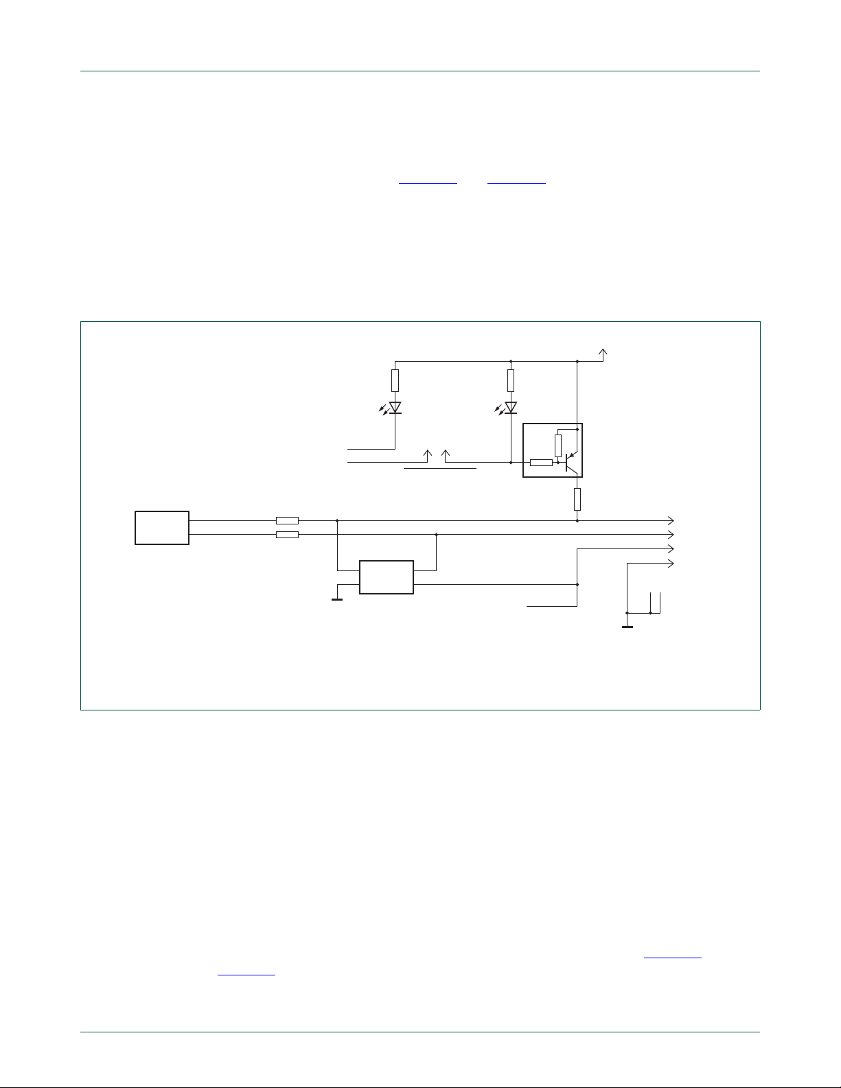
5.10 Logic probe
Most of the I2C-bus slaves produce logic signals on their input/output ports. It is necessa ry
to know a logic state. To facilitate this test there are two LEDs with buffers that may be
used as a simple ‘logic probe’.
UM10741
Fm+ development kit OM13320
To prevent circuit loading the LEDs are buffered by FETs as shown in Figure 46
. Green
LED (D6) is driven by FET (Q2) when CN11-1 is at or near ground. When CN11-1 is open
(or logic 1) the FET is non-conducting, and the LED is off. Red LED (D7) is driven by FET
(Q3) when CN11-4 is at or near ground. When CN11-4 is open (or logic 1) the FET is
non-conducting, and the LED is off. See Figure 47
Note that the threshold voltage (V
) of the FET is 2.5 V to 4.5 V to ensure it operates
th
.
correctly on both 3.3 V and 5 V logic levels. The FET source is tied to 5 V, and the gate
must therefore be at 2.5 V or lower relative to ground, to turn on the FET and light the
LED.
Fig 46. Logic probe circuit
UM10741 All information provided in this document is subject to legal disclaimers. © NXP B.V. 2014. All rights reserved.
User manual Rev. 1 — 1 April 2014 35 of 61

NXP Semiconductors
UM10741
Fm+ development kit OM13320
Fig 47. Logic probe section (shown monitoring two GPIO channels from Bus1)
5.11 INT and RST indicators
Two global digital signal nets, called INT (interrupt) and RST (reset), connect all I2C-bus
devices on the board and also the Port A – Port E daughter card connectors. These are
also connected to the Master (MCU, IC5) on Bus1, the Master (Bus Controller, IC4), and
the LPC Xpresso module. See Figure 48
Additional buffered LEDs are provided (D19, RST and D20, Interrupt) on the Fm+
Development Board (OM13260) for visual indication. These buffered LEDs operate in the
same fashion as the logic probe (see Section 5.10 “
+3V3
INT
10 kΩ
R9
Q4
SI2325DS
+5V
R8
820 Ω
D20
LTST-C170CKT RED
RED
INT LED
GND
and Figure 49.
Logic probe”).
+3V3
R10
10 kΩ
RESET
Q5
SI2325DS
+5V
R7
820 Ω
D19
LTST-C170CKT RED
RED
RST LED
GND
aaa-012048
Fig 48. INT an d RST indicators circuit
UM10741 All information provided in this document is subject to legal disclaimers. © NXP B.V. 2014. All rights reserved.
User manual Rev. 1 — 1 April 2014 36 of 61

NXP Semiconductors
UM10741
Fm+ development kit OM13320
Fig 49. INT and RST indicators section
5.12 Prototype area
Additional circuits may be required to for an application beyond the intended scope of the
Fm+ Development Board (OM13260). For e xample, using dif f erent value p ull-up resistors
than those supplied, or other circuit experiments.
The prototype area is available, and consists of pads and holes on a 100 mil (2.54 mm)
grid. Power for these components is made available at several connector points (CN15 is
ground, CN21 is +3.3 V, and CN22 is +5 V). See Figure 50
and Figure 51.
UM10741 All information provided in this document is subject to legal disclaimers. © NXP B.V. 2014. All rights reserved.
User manual Rev. 1 — 1 April 2014 37 of 61

NXP Semiconductors
aaa-012049
UTILITY POWER
+5V
CN22-4
CN22-2
CN22-3
CN22-1
+3V3
CN21-4
CN21-2
CN21-3
CN21-1
CN15-4
CN15-2
CN15-3
CN15-1
GND
UM10741
Fm+ development kit OM13320
Fig 50. Prototype area circuit
Fig 51. Prototype area section
UM10741 All information provided in this document is subject to legal disclaimers. © NXP B.V. 2014. All rights reserved.
User manual Rev. 1 — 1 April 2014 38 of 61

NXP Semiconductors
5.13 LED blinker (PCA9901)
UM10741
Fm+ development kit OM13320
On the Fm+ Development Board (OM13260) V3.0 there is an LED Blinker device
(PCA9901, IC3) and LED indicator (D10). While not strictly an I
one-wire protocol, it belongs to the NXP I
2
C-bus product portfolio.
2
C-bus device, as it uses a
Remark: The PCA9901 will be made obsolete, and will not be present on future versions
of the Fm+ Development Board (OM13260).
Refer to the PCA9901 data sheet for det ails of th is device. Note that it is not connected to
2
either I
C Bus on the Fm+ Development Board (OM13260). It is connected to the LPC
Xpresso module (PIO_0.7), and that module must be present (and programmed) to drive
the PCA9901 device. See Figure 52
GND
D10
LTST-C170CKT RED
GND
and Figure 53.
IC3
1
GND
2
LEDOUT
4
ISET
R19
PCA9901DP
47 kΩ
GND
PCA9901 LED BLINKER
VDD
TEST1
CTRL
8
7
5 P0.7
GND
aaa-012137
Fig 52. LED blinker (PCA9901)
Fig 53. LED blinker (PCA9901) section
UM10741 All information provided in this document is subject to legal disclaimers. © NXP B.V. 2014. All rights reserved.
User manual Rev. 1 — 1 April 2014 39 of 61

NXP Semiconductors
6. GPIO target board (OM13303)
The GPIO Target Board (OM13303) is used to monitor the Input/Output (I/O) signals from
a GPIO. The board has eight channels, each with a push switch and an LED indicator.
See Figure 54
Fig 54. OM13303 GPIO target board PCB assembly (front side)
6.1 Theory of operation
.
UM10741
Fm+ development kit OM13320
Each of the eight channels operates independently and in the same way. The voltage
applied to the input pin is compared in a Windows comparator, which in tur n drives a d ua l
color LED. The thresholds for the comparators are set to one-third (logic zero) and
two-thirds (logic one) of the supply voltage. These values correspond to the I
threshold voltages for the I
2
C-bus specification.
2
C-bus logic
When a push button is pressed, a logic zero is applied the channel, which can be r ead by
the GPIO device to which the GPIO Target Board is attached. A 2 × 5 header is used to
connect to the Fm+ Development Board (OM13260) or a GPIO daughter card with a flat
ribbon cable (supplied in the kit).
Two connectors are installed, one on each end of the board, and on opposite sides of the
PCB to aid in connection without the cables blocking the buttons or LEDs.
There are no option jumpers and no adjustments on the GPIO Target Board (OM13303).
Unlike other PCB assemblies in the Fm+ Development Kit (OM13320), the GPIO Target
Board (OM13303) has components on both sides of the PCB. See Figure 55
.
Fig 55. OM13303 GPIO target board PCB assembly (back side)
UM10741 All information provided in this document is subject to legal disclaimers. © NXP B.V. 2014. All rights reserved.
User manual Rev. 1 — 1 April 2014 40 of 61

NXP Semiconductors
6.2 Circuit description
The schematic diagram has multiple sheets. For clarification, only fragments of the
schematic are shown here. The full schematic should be downloaded if required. The
following pages are divided in to several sections covering the win dow comparator, push
switches, bias circuit, and connectors.
6.2.1 Window comparator
Channel 0 is shown; channels 1 through 7 are identical. The input signal is applied to two
comparators, (IC01A and IC01B).
UM10741
Fm+ development kit OM13320
If the input (IO0) is higher than the threshold set by V
and resistor divider (R03 and
IH
R04), the output of the comparator (IC01A) switches to near ground. This turns on the
green LED (D01). Resistor (R04) applies positive feedback hysteresis (about 150 mV) to
the comparator, shifting the trip point to a slightly lower voltage, to stop the circuit from
oscillation around the switch point.
The input (IO0) is attenuated slightly by a resistor divider (R07 and R08), if the resulting
voltage is lower than the threshold set by V
, the output of the comparator (IC1B)
IL
switches to near ground. This turns on the red LED (D01). Resistor (R08) applies positive
feedback hysteresis (about 125 mV) to the comparator, shifting the trip point to a slightly
higher voltage, to stop the circuit from oscillation around the switch point.
LED current is limited by resistors R05 and R09, which are selected to give approximately
equal brightness to the green and red LED elements. See Figure 56
.
The operation of the window circuit is shown by applying a ramp waveform, see Figure 57
and Figure 58
.
+3V3
R02
VH
IO0
VL
10 kΩ
R03
51 kΩ
R06
10 kΩ
R07
51 kΩ
2
3
6
5
R04
1 MΩ
LMV358MM
1
IC01A
LMV358MM
1
IC01B
R05
330 Ω
GR
DUAL_LEDLTST
D01
R08
1 MΩ
R09
820 Ω
aaa-012138
Fig 56. Window comparator (Channel 0 shown)
UM10741 All information provided in this document is subject to legal disclaimers. © NXP B.V. 2014. All rights reserved.
User manual Rev. 1 — 1 April 2014 41 of 61

NXP Semiconductors
Fig 57. Input ramp (yellow trace), green LED drive (green trace)
UM10741
Fm+ development kit OM13320
Fig 58. Input ramp (yellow trace), red LED drive (green trace)
UM10741 All information provided in this document is subject to legal disclaimers. © NXP B.V. 2014. All rights reserved.
User manual Rev. 1 — 1 April 2014 42 of 61

NXP Semiconductors
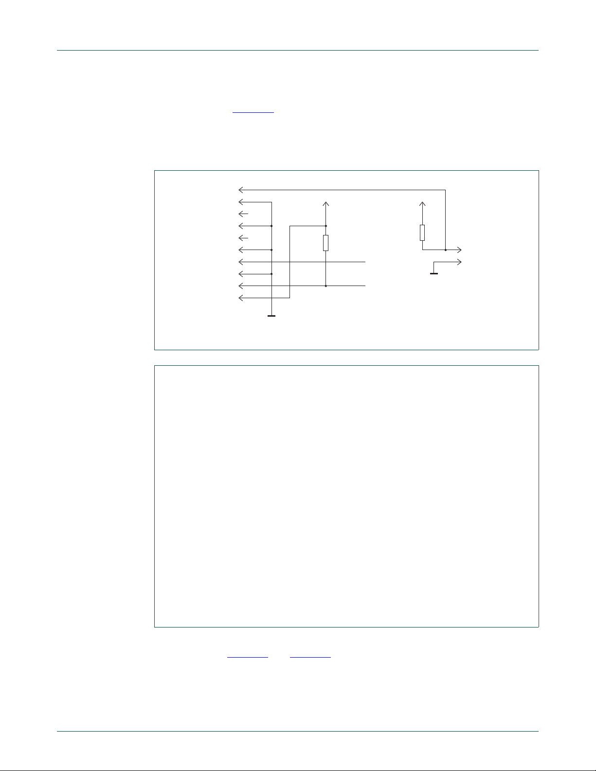
6.2.2 Push switches
Each channel has a push switch (S01 through S71) that connects the appropriate IO pin
to ground when pressed. Series resistors (R01 th rough R71) lim it the current, in the event
that the IO pin is being driven HIGH (by the connected GPIO device) when the push
switch is closed. Each input is biased to VC (one-half the supply volt age), in the event that
the IO pin is left open. This extinguishes both the green and red LEDs of that channel,
preventing false readings. See Figure 59
UM10741
Fm+ development kit OM13320
.
VC
R102
IO0
R01
1
2
3
4
S01
GND
Fig 59. Push switches
6.2.3 Bias circuit
Each channel requires three reference voltag es (VL, VC, and VH), from the bias circuit.
A resistor divider chain (R01, R02, R0 3, and R04) divides the supply voltage to produce
one-third (VL), one half (VC) and two-thirds (VH). Each value is buffered by an op amp
(sections of IC80). Test points are provided as PCB pads for VH (high), VC (center), and
VL (low). The fourth section of the quad op amp (IC80) is not used. Noise spikes on each
bias supply are removed by capacitors (C89, C90, and C91), powe r supply variations are
removed by capacitors (C86 and C87). See Figure 60
10 kΩ
270 Ω
S11
IO1
R112
R11
1
3
GND
10 kΩ
270 Ω
S31
IO3
R132
R31
1
3
GND
2
4
R122
10 kΩ
IO2
R21
270 Ω
1
S21
3
GND
2
4
2
4
10 kΩ
270 Ω
S41
IO4
1
3
GND
R142
R41
2
4
10 kΩ
270 Ω
S51
IO5
R152
R51
1
3
GND
2
4
10 kΩ
270 Ω
S61
IO6
R162
R61
1
3
GND
2
4
10 kΩ
270 Ω
R172
IO7
R71
1
2
3
4
S71
GND
aaa-012139
10 kΩ
270 Ω
.
UM10741 All information provided in this document is subject to legal disclaimers. © NXP B.V. 2014. All rights reserved.
User manual Rev. 1 — 1 April 2014 43 of 61

NXP Semiconductors
+3V3
R81
R82
R83
R84
GND
10 kΩ
5.1 kΩ
GND
5.1 kΩ
10 kΩ
GND
13
12
C87
4.7 μF, 6.3 V
C86
4.7 μF, 6.3 V
VL
10
6
5
2
3
9
14
IC80D
LMV324MZ
7
IC80B
LMV324MZ
1
IC80A
LMV324MZ
8
IC80C
LMV324MZ
UM10741
Fm+ development kit OM13320
TP3
VH
VH
C89
100 nF
GND
TP4
VC
VC
C90
100 nF
GND
TP2
VL
VL
C91
100 nF
GND
aaa-012140
Fig 60. Bias circuit
6.2.4 Connectors
The GPIO Target Board (OM13303) is intended to be connected to the Fm+ Development
Board (OM13260) (or other GPIO daughter cards) via a 10-pin ribbon cable. There are
two identical connectors, one on each end of the GPIO Target Board to allow connection
without blocking the push switches or the LEDs. See Figure 61
Fig 61. Connectors
GND
+3V3
+3V3
GND
IO0
IO1
IO2
IO3
IO4
IO5
IO6
IO7
CN1-1
CN1-2
CN1-3
CN1-4
CN1-5
CN1-6
CN1-7
CN1-8
CN1-9
CN1-10
GND
+3V3
+3V3
GND
IO0
IO1
IO2
IO3
IO4
IO5
IO6
IO7
, Figure 62 and Figure 63.
CN2-1
CN2-2
CN2-3
CN2-4
CN2-5
CN2-6
CN2-7
CN2-8
CN2-9
CN2-10
aaa-012141
UM10741 All information provided in this document is subject to legal disclaimers. © NXP B.V. 2014. All rights reserved.
User manual Rev. 1 — 1 April 2014 44 of 61

NXP Semiconductors
UM10741
Fm+ development kit OM13320
Fig 62. Ribbon cables attached to underside of the GPIO target board (OM13303)
Fig 63. Ribbon cables attached to the topside of the GPIO target board (OM13303)
UM10741 All information provided in this document is subject to legal disclaimers. © NXP B.V. 2014. All rights reserved.
User manual Rev. 1 — 1 April 2014 45 of 61

NXP Semiconductors
7. Bus buffer demo board (OM13398)
The Bus Buffer Board (OM13398) (supplied in the kit) provides a method to link both the
2
I
C buses on the Fm+ Development Board (OM1326 0) by attachment to Port E, in place
of the wire jumper used earlier (see Section 5.6.1 “
jumper)”. See Figure 64 and Figure 65.
UM10741
Fm+ development kit OM13320
Linking both buses together (with a
Fig 64. Bus buffer board (OM13398)
Fig 65. Bus buffer board (OM13398) attached to the Fm+ development board (OM13260)
UM10741 All information provided in this document is subject to legal disclaimers. © NXP B.V. 2014. All rights reserved.
User manual Rev. 1 — 1 April 2014 46 of 61

NXP Semiconductors
7.1 Theory of operation
Two identical bus buffer devices are connected in series between the Bus1 and Bus2
segments on the Fm+ Development Board (OM13260). Ea ch Bus Buf fer has two identica l
channels, one for I
will be described in detail.
UM10741
Fm+ development kit OM13320
2
C clock (SCL) and the second for I2C data (SDA). Only one channel
Each PCA9617A bus buffer device has two p ower supply conn ections, V
to allow voltage level shifting between one I
2
C-bus segment and another I2C-bus
CC(A)
segment. Jumpers on the Bus Buffer Boar d ( OM133 98 ) select th e voltage source of each
of the two device power supplies. To demonstrate the voltage level translator ability the
link between the two bus buffers is supplied from a variable voltage regulator, which in
turn can be set by the user anywhere between 1.0 V and 3.2 V.
The pull-up resistor on the Low Voltage Bus section is selected by jumpers.
7.2 Circuit description
The schematic diagram has multiple sheets. For clarification, only fragments of the
schematic are shown here. The full schematic should be downloaded if required. The
following pages are divided in to several sections covering the Bu s1 Bus Buf fer, Bus2 Bus
Buffer, Supply select jumpers, Adjustable Voltage Regulator , and Connectors. A block
diagram will assist understanding. See Figure 66
5 V
ADJUSTABLE
VOLTAGE
REGULATOR
1.0 V to 3.2 V
V
CC(B)
V
V
CC(A)
JP2
CC(A)
3.3 V
PULL-UP
RESISTORS
V
CC(A)
.
5 V
JP1
3.3 V
V
CC(B)
V
CC(A)
V
CC(B)
and V
CC(B)
,
BUS1
BA
PCA9617A
low
voltage
bus
AB
PCA9617A
BUS2
aaa-012142
Fig 66. Block diagram for the bus buffer board (OM13398)
UM10741 All information provided in this document is subject to legal disclaimers. © NXP B.V. 2014. All rights reserved.
User manual Rev. 1 — 1 April 2014 47 of 61

NXP Semiconductors
7.2.1 Bus1 bus buffer (PCA9617A)
I2C-bus signals from the Fm+ Development Board (OM13260), called SCL1 an d SDA1,
are applied to the high voltage or ‘B’ Side of IC1 (PCA9617A). The required pull-up
resistors on this section of Bus1 are on the Fm+ Development Board (OM13260).
Signals on the low voltage or ‘A’ Side of IC1 are connected to a selection of pull-up
resistors selected by either JP5 (for SCL) or JP3 (for SDA), and the low voltage or ‘A’ Side
of the second PCA9617A, IC3.
Loading capacitors, C31 for SCL and C51 SDA, can be place d on the low voltage section
of the bus. To accommodate two different footprints IC1 (TSSOP8) and IC2 (HWSON8)
are connected in parallel, but only one part is installed. Installing JP4 disables the Bus
Buffer. See Figure 67
UM10741
Fm+ development kit OM13320
.
V
DD(A)
TP1
SCL1
SDA1
TSSOP8
HWSON8
SDA VDD(A) PULL-UP
C7
100 nF
TP2
6
SCL1
7
SDA1
C9
100 nF
SCL1
SDA1
4
5
DO NOT PLACE
SDAB
SCLB
SDAB
SCLB
V
DD(A)
V
DD(B)
1
8
VDD(B)
VDD(A)
GND
4
PCA9617ADP
GND
V
DD(A)
V
DD(B)
7
6
VDD(B)
VDD(A)
GND
2
PCA9617ATP
GND
SDAA
SCLA
EN
SDAA
SCLA
EN
IC1
32SCLA
5
IC2
1
8
3
C52
100 nF
C8
GNDGND
C10
GNDGND
GND
100 nF
SDAA
100 nF
R51
JP3-2
JP3-1
SCLA
SDAA
R52
240 Ω
GND
ENABLE
524 Ω
JP3-4
JP3-3
R53
JP4-1
JP4-2
3.0 kΩ
JP3-6
JP3-5
JP3-8
JP3-7
C51
100 pF
GND
aaa-012143
Fig 67. Bus1 bus buffer
UM10741 All information provided in this document is subject to legal disclaimers. © NXP B.V. 2014. All rights reserved.
User manual Rev. 1 — 1 April 2014 48 of 61

NXP Semiconductors
7.2.2 Bus2 bus buffer (PCA9617A)
I2C-bus signals on the low voltage bus are also connected to the A side of the second
PCA9617A Bus Buffer device, IC3. To accommodate two different footprints, IC3
(TSSOP8) and IC4 (HWSON8) are connected in parallel, but only one device is installed.
Installing JP6 disables the bus buffer. See Figure 68
2
C-bus signals from the high voltage or ‘B’ side of IC3 (PCA9617A) are passed back to
I
the Fm+ Development Board (OM13260). The required pull-up resistors on this section of
Bus1 are on the Fm+ Development Board (OM13260).
V
DD(A)
UM10741
Fm+ development kit OM13320
.
TP3
SCLA
C32
100 nF
SDAA
GND
TP4
R31
240 Ω
JP5-2
JP5-1
R32
524 Ω
JP5-4
JP5-3
JP6-1
JP6-2
ENABLE
R33
3.0 kΩ
JP5-6
JP5-5
GND
SCL VDD(A) PULL-UP
C31
JP5-8
JP5-7
SCLA
SDAA
100 pF
GND
GND GND
SCLA
SDAA
GND GND
V
DD(A)
C4
100 nF
IC3
3
SDAA
2
SCLA
5
EN
PCA9617ADP
V
DD(A)
C6
100 nF
IC4
1
SDAA
8
SCLA
3
EN
PCA9617ATP
V
DD(B)
1
VDD(A)
GND
V
DD(B)
7
VDD(A)
GND
8
SDAB
VDD(B)
SCLB
GND
4
6
SDAB
VDD(B)
SCLB
GND
2
DO NOT PLACE
C3
6
7
C5
4
5
100 nF
SCL2
SDA2
TSSOP8
100 nF
SCL2
SDA2
HWSON8
TP5
SCL2
TP6
SDA2
aaa-012144
Fig 68. Bus2 bus buffer
UM10741 All information provided in this document is subject to legal disclaimers. © NXP B.V. 2014. All rights reserved.
User manual Rev. 1 — 1 April 2014 49 of 61

NXP Semiconductors
aaa-012145
GND
JP1-1
JP1-2
JP1-3
V
DD(B)
+5V
+3V3
SEL VDD(B) VOLTAGE
JP2-1
JP2-2
JP2-3
V
DD(A)
+3V3
+5V +5V
SEL VDD(A) VOLTAGE
D2
LTST-C170TBKT(BLU)
10 kΩ
R6
820 Ω
R2
V
DD(A)
TP7
51 kΩ
R3
C1
22 pF/16 V
1.64 kΩ
R7
BLU
GND
Q1
BSH111
VDD(A) ON
+5V
R4
50 kΩ
22 kΩ
R5
GND
GND
IC5
FAN2558ADJ
1
3
2
VIN
EN
GND
VOUT
ADJ
PG
6
5
4
VDD(A) LDO
1.0 V to 3.2 V
VAR ADJ
7.2.3 Supply select jumpers
The ‘B Side’ (high voltage side of the voltage level translator) of each PCA9617A can be
either 3.3 V or 5 V as selected by JP1. The ‘A Side’ (low voltage side of the voltage level
translator) of each PCA9617A can be either 3.3 V or a var iable voltage between 1.0 V and
3.2 V as selected by JP2. See Figure 69
UM10741
Fm+ development kit OM13320
.
UM10741 All information provided in this document is subject to legal disclaimers. © NXP B.V. 2014. All rights reserved.
User manual Rev. 1 — 1 April 2014 50 of 61
Fig 69. Supply select jumpers
7.2.4 Variable voltage regulator
.
The low voltage bus bias is generated by an LDO (Low Drop Out) voltage regulator, IC5.
The output voltage is set by resistor divider R3, R4, and R5, and provides a range of 1.0 V
to 3.2 V. The LDO provides a ‘Power Good’ signal, which is pulled HIGH by R6, and
buffered by Q1. When the LDO is working correctly, the blue LED (D2) is turned ON.
See Figure 69

NXP Semiconductors
aaa-012146
CN1-14
SCL1
CN1-13
CN1-12
INT
CN1-11
RESET
CN1-10
+5V
CN1-9
+3V3
CN1-8
CN1-7
GND
CN1-6
+3V3
CN1-5
+5V
SDA2
GND
CN1-4
CN1-3
INT
CN1-2
SDA1
CN1-1
SCL2
RESET
Fm+ BOARD PORT E
aaa-012147
135791113
2 4 6 8 10 12 14
SCL2
INT
5V
GND
3V3
RESET
SDA2
SDA1
RESET
3V3
GND
5V
INT
SCL1
7.2.5 Connector
The connector on the Bus Buffer Board (OM13398) matches the Port E connector on the
Fm+ Development Board (OM13260). See Figure 70
The signals are arranged to be symmetrical so that the Bus Buffer Board (OM13398) can
be rotated 180°, causing the signals from the Fm+ Development Board (OM13260) to flow
in the opposite direction. For example, from Bu s1 to Bus2, or from Bus2 to Bus1 when the
Bus Buffer Board (OM13398) is rotated in th e Port E connector . See Figure 71
to reverse the signal flow is necessary when examining differ ent I
one NXP device to a non-NXP device.
UM10741
Fm+ development kit OM13320
and Figure 71.
2
C buffers, or comparing
. The ability
UM10741 All information provided in this document is subject to legal disclaimers. © NXP B.V. 2014. All rights reserved.
User manual Rev. 1 — 1 April 2014 51 of 61
Fig 70. Bus buffer board connector
Fig 71. Fm+ development board Port E connector

NXP Semiconductors
8. Bridge board (OM13399)
UM10741
Fm+ development kit OM13320
The Bridge Board (OM13399) (supplied in the kit) provides attachment of old style with a
9-pin, in-line, non-polarized connector NXP designed I
2
C demo boards to the
Fm+ Development Board (OM13260). The Bridge Board (OM13399) can attach to any
daughter card Port (A – D) inclusive. See Figure 72
and Figure 73.
Fig 72. Bridge boar d (OM13399 attached to the Fm+ development board (OM13260)
Fig 73. Bridge boar d (OM13399)
UM10741 All information provided in this document is subject to legal disclaimers. © NXP B.V. 2014. All rights reserved.
User manual Rev. 1 — 1 April 2014 52 of 61
NXP Semiconductors
8.1 Theory of operation
UM10741
Fm+ development kit OM13320
The Bridge Board is mostly a mechanical platform for the old style with a 9-pin, in-line,
non-polarized connector of NXP designed I
position connector. Previous NXP I
2
C demo boards were released with both vertical and
2
C demo boards that use a non-polarized nine
horizontal mounting, and both male pins and female sockets. The Bridge Board
(OM13399) therefore has both styles. There is also a ‘Tester’ connector that allows direct
connection of the third-party tools (see Section 9
non-polarized nine-circuit connector had only one I
). The old style with a 9-pin, in-line,
2
C-bus, with SCL and SDA signals.
The Fm+ Development Board Daughter Card ports have two I
signals. One or other I
2
C Bus can be selected by jumpers. The power source may also be
selected by jumper.
8.2 Circuit description
The schematic diagram has a single sheet. For clarification, only fragments of the
schematic are shown here. The full schematic should be downloaded if required. The
circuit is simple.
8.2.1 Fm+ development board (OM13260) connector (CN3)
CN3-14
CN3-13
CN3-12
CN3-11
CN3-10
CN3-9
CN3-8
CN3-7
CN3-6
CN3-5
CN3-4
CN3-3
CN3-2
CN3-1
Fm+ BOARD
SCL1
SDA2
INT
RESET
+5V
+3V3
GND
GND
+3V3
+5V
RESET
INT
SDA1
SCL2
SCL
SDA
2
C Buses (Bus1 and Bus2)
JP2-3
JP2-2
JP2-1
JP3-3
JP3-2
JP3-1
SEL Fm+ BUS
1
2
1
2
aaa-012148
Fig 74. Fm+ development board (OM13260) connector (CN3)
The connector on the Bridge Board (OM13399) matches the Port connectors on the
Fm+ Development Board (OM13260) See Figure 74
. A Bridge Board (OM13399) can be
attached to any Port A – Port D inclusive. It cannot be connected to Port E due to
mechanical arrangement of the Port E connector.
2
The Fm+ Development Board has two separate I
C buses (Bus1 and Bus2) and one of
these is selected by two jumpers, JP2 for SCL and JP3 for SDA.
UM10741 All information provided in this document is subject to legal disclaimers. © NXP B.V. 2014. All rights reserved.
User manual Rev. 1 — 1 April 2014 53 of 61
NXP Semiconductors
aaa-012149
SEL POWER SOURCE
JP4-2
JP4-1
JP4-3
+3V3
VDD
JP1-1
JP1-3
JP1-2
PWRVDD
+5V
5V_TSTR
aaa-012150
CN1-1
+5V
CN1-2
CN1-3
+3V3
CN1-4
+3V3SW
CN1-5
SCL
CN1-6
GND
CN1-7
CN1-8
CN1-9
+5VSW
SDA
9POS FEMALE SOCKET
RESET
INT
CN2-1
+5V
CN2-2
CN2-3
+3V3
CN2-4
+3V3SW
CN2-5
SCL
CN2-6
GND
CN2-7
CN2-8
CN2-9
+5VSW
SDA
9POS MALE HEADER
RESET
INT
8.2.2 Power supply select (JP1 and JP4)
Fig 75. Power supply selector
There are two power sources available to the Bridge Board (OM13399) depending upon
whether it is connected to the Fm+ Development Board (OM13260) or powered by a
third-party tool (see Section 9
UM10741
Fm+ development kit OM13320
).
The Tester socket provides 5 V and the Fm+ Development Board (OM13260) provides
both 3.3 V or 5 V. Jumper JP1 selects the source of the 5 V power. JP4 selects either
3.3 V or 5 V as needed.
Remark: When the Bridge Board (OM13399) is not attached to the Fm+ Development
Board and powered by the Tester, the only option is 5 V.
8.2.3 9-position connectors (CN1 and CN2)
Fig 76. 9-position connectors (CN1 and CN2)
UM10741 All information provided in this document is subject to legal disclaimers. © NXP B.V. 2014. All rights reserved.
User manual Rev. 1 — 1 April 2014 54 of 61
Two 9-position connectors are provided; both carry exactly the same signals. CN1 is
female, CN2 is male.
Remark: These connectors are not polarized or keyed. Take care to make connection
correctly.

NXP Semiconductors
aaa-012151
CN4-10
GND
CN4-9
CN4-8
CN4-7
CN4-6
5V_TSTR
CN4-5
CN4-4
CN4-3
SDA
CN4-2
GND
CN4-1
SCL
I2C TESTER
PWR
aaa-012152
RESET
INT
R5
10 kΩ
GND
D2
R2
820 Ω
VDD
INT
LTST-C150KRKT(RED)
D1
R1
820 Ω
VDD
LTST-C150KGKT(GRN)
VDD1
SDA
SCL
R3
10 kΩ
VDD
R4
10 kΩ
VDD
8.2.4 Tester connector (CN4)
Fig 77. Tester connection (CN4)
The 10-position (2 × 5) shrouded header connector (CN4) mates with third-party tools
(see Section 9
UM10741
Fm+ development kit OM13320
). Only I2C-bus signals and available 5 V power ar e co nn ec te d.
Remark: The Tester’s bus signals are connected to the two 9-position connectors and,
depending upon the position of JP2 and JP3, to the Fm+ Development Board Bus1 or
2
Bus2. Take care to avoid double termination of the I
C buses.
8.2.5 LED indicators and pull-ups
Fig 78. LED indicators and pull-ups
UM10741 All information provided in this document is subject to legal disclaimers. © NXP B.V. 2014. All rights reserved.
User manual Rev. 1 — 1 April 2014 55 of 61
Two LEDs provide indication of power (D1, Green) and INT (interrupt) status (D2, Red). To
prevent malfunction of the I
does not have pull-up on either SCL or SDA, there are weak pull-ups (R3, R4). These may
2
C-bus if the Bridge Board (OM13399) is used in manner that
be replaced with lower value resistors (or removed), as needed.

NXP Semiconductors
8.3 Example using PCA9632 (OM13269)
UM10741
Fm+ development kit OM13320
Fig 79. Bridge boar d (OM13399) used to attach a PCA9632 (OM13269)
The Bridge Board (OM13399) (supplied in the kit) provides attachment of old style with a
9-pin, in-line, non-polarized connector NXP designed I
2
C demo boards to the
Fm+ Development Board (OM13260).
UM10741 All information provided in this document is subject to legal disclaimers. © NXP B.V. 2014. All rights reserved.
User manual Rev. 1 — 1 April 2014 56 of 61

NXP Semiconductors
9. Third-party tools
Generation, inspection and logging of I2C-bus data is easily achieved with third-party
development tools from a number of suppliers: SB Solutions, Inc. (www.i2ctools.com
Total Phase (www.totalphase.com
SB Solutions supplies a range of tools driven from USB and outputs to I
user interface is very similar to the Fm+ Development Board GUI, and a DLL is provided
for custom development. These tools are not supplied in the kit, and must be purchased
directly from the vendor.
Total Phase supplies two tools called Aardvark (host adapter) and Beagle (bus logger)
that connect directly to the Fm+ Development Board (OM13260). These tools are not
supplied in the kit, and must be purchased directly from the vendor.
UM10741
Fm+ development kit OM13320
) and
).
2
C and SPI. The
Fig 80. SB Solutions USB-to-I2C Pro connected to an Fm+ Develop ment Board
daughter card
Fig 81. Aardvark Host Adapter connected to the Fm+ development board (OM13260)
UM10741 All information provided in this document is subject to legal disclaimers. © NXP B.V. 2014. All rights reserved.
User manual Rev. 1 — 1 April 2014 57 of 61

NXP Semiconductors
UM10741
Fm+ development kit OM13320
Fig 82. Beagle Bus Logger connected to the Fm+ development board (OM13260)
UM10741 All information provided in this document is subject to legal disclaimers. © NXP B.V. 2014. All rights reserved.
User manual Rev. 1 — 1 April 2014 58 of 61

NXP Semiconductors
10. Abbreviations
Table 7. Abbreviations
Acronym Description
DLL Dynamic Link Library
EVM Evaluation Module
FET Field-Effect Transistor
Fm+ Fast-mode Plus
GPIO General Purpose Input/Output
GUI Graphical User Interface
HID Human Interface Driver
2
C-bus Inter-Integrated Circuit-bus
I
I/O Input/Output
ISP In-System Programmable
JTAG Joint Test Action Group
LDO Low Drop-Out
LED Light-Emitting Diode
MCU MicroController Unit
OS Operating System
PC Personal Computer
PCB Printed-Circuit Board
RC Resistor-Capacitor network
RGB Red/Green/Blue
SPI Serial Peripheral Interface
SWD Single Wire Debug
USB Universal Serial Port
UM10741
Fm+ development kit OM13320
11. References
[1] UM10785, “Fm+ Demo Board Software Installation Guide” —
NXP Semiconductors; 25 February 2014;
www.nxp.com/documents/user_manual/UM10785.pdf
UM10741 All information provided in this document is subject to legal disclaimers. © NXP B.V. 2014. All rights reserved.
User manual Rev. 1 — 1 April 2014 59 of 61

NXP Semiconductors
12. Legal information
UM10741
Fm+ development kit OM13320
12.1 Definitions
Draft — The document is a draft version only. The content is still under
internal review and subject to formal approval, which may result in
modifications or additions. NXP Semiconductors does not give any
representations or warranties as to the accuracy or completeness of
information included herein and shall have no liability for the consequences of
use of such information.
12.2 Disclaimers
Limited warranty and liability — Information in this document is believed to
be accurate and reliable. However, NXP Semiconductors does not give any
representations or warranties, expressed or implied, as to the accuracy or
completeness of such information and shall have no liability for the
consequences of use of such information. NXP Semiconductors takes no
responsibility for the content in this document if provided by an information
source outside of NXP Semiconductors.
In no event shall NXP Semiconductors be liable for any indirect, incidental,
punitive, special or consequential damages (including - without limitation - lost
profits, lost savings, business interruption, costs related to the removal or
replacement of any products or rework charges) whether or not such
damages are based on tort (including negligence), warranty, breach of
contract or any other legal theory.
Notwithstanding any damages that customer might incur for any reason
whatsoever, NXP Semi conductors’ aggregat e and cumulative liabil ity towards
customer for the products described herein shall be limited in accordance
with the Terms and conditions of commercial sale of NXP Semiconductors.
Right to make changes — NXP Semiconductors reserves the right to make
changes to information published in this document, including without
limitation specifications and product descriptions, at any time and without
notice. This document supersedes and replaces all information supplied prior
to the publication hereof.
Suitability for use — NXP Semiconductors products are not designed,
authorized or warranted to be suitable for use in life support, life-critical or
safety-critical systems or equipment, nor in applications where failure or
malfunction of an NXP Semiconductors product can reasonably be expected
to result in personal injury, death or severe property or environmental
damage. NXP Semiconductors and its suppliers accept no liability for
inclusion and/or use of NXP Semiconductors products in such equipment or
applications and therefore such inclusion and/or use is at the cu stomer’s own
risk.
Applications — Applications that are described herein for any of these
products are for illustrative purposes only. NXP Semiconduct ors makes no
representation or warranty that such applications will be suitable for the
specified use without further testing or modification.
Customers are responsible for the design and operation of their applications
and products using NXP Semiconductors product s, and NXP Semiconductors
accepts no liability for any assistance with applications or customer product
design. It is customer’s sole responsibility to determine whether the NXP
Semiconductors product is suitable and fit for the customer’s applications and
products planned, as well as for the planned application and use of
customer’s third party customer(s). Customers should provide appropriate
design and operating safeguards to minimize the risks associated with their
applications and products.
NXP Semiconductors does not accept any liability related to any default ,
damage, costs or problem which is based on any weakness or default in the
customer’s applications or products, or the application or use by customer’s
third party customer(s). Customer is responsible for doing all necessary
testing for the customer’s applications and products using NXP
Semiconductors products in order to avoid a default of the applications and
the products or of the application or use by customer’s third part y
customer(s). NXP does not accept any liability in this respect.
Export control — This document as well as the item(s) described herein
may be subject to export control regulations. Export might require a prior
authorization from competent authorities.
Evaluation products — This product is provided on an “as is” and “with all
faults” basis for evaluation purposes only. NXP Semiconductors, its affiliates
and their suppliers expressly disclaim all warranties, whet her express, implied
or statutory, including but not limited to the implied warranties of
non-infringement, merchantability and fitness for a particular purpose. The
entire risk as to the quality, or arising out of the use or performance, of this
product remains with customer.
In no event shall NXP Semiconductors, its affiliates or their su ppliers be liable
to customer for any special, indirect, consequential, punitive or incidental
damages (including without limitation damages for l oss of bu siness, busi ness
interruption, loss of use, loss of data or information, and the like) arising out
the use of or inability to use the product, whether or not based on tort
(including negligence), strict liability, breach of contract, breach of warranty or
any other theory , even if advised of the possibility of such damages.
Notwithstanding any damages that customer might incur for any reason
whatsoever (including without limitation, all damages referenced above and
all direct or general damages), the entire liability of NXP Semiconductors, its
affiliates and their suppliers and customer’s exclusive remedy for all of the
foregoing shall be limited to actual damages incurred by customer based on
reasonable reliance up to the greater of the amount actually paid by customer
for the product or five dollars (US$5.00). The foregoin g limita tions, exclusions
and disclaimers shall apply to the maximum extent permitted by applicable
law, even if any remedy fails of its essential purpose.
Translations — A non-English (translated) version of a document is for
reference only. The English version shall prevail in case of any discrepancy
between the translated and English versions.
12.3 Trademarks
Notice: All referenced brands, prod uct names, service names and trademarks
are the property of their respective owners.
2
I
C-bus — logo is a trademark of NXP Semiconductors N.V.
UM10741 All information provided in this document is subject to legal disclaimers. © NXP B.V. 2014. All rights reserved.
User manual Rev. 1 — 1 April 2014 60 of 61

NXP Semiconductors
13. Contents
UM10741
Fm+ development kit OM13320
1 Introduction . . . . . . . . . . . . . . . . . . . . . . . . . . . . 3
2 Key features. . . . . . . . . . . . . . . . . . . . . . . . . . . . 3
I2C-bus masters . . . . . . . . . . . . . . . . . . . . . . . . .3
I2C-bus slaves . . . . . . . . . . . . . . . . . . . . . . . . . .3
Accessory sockets . . . . . . . . . . . . . . . . . . . . . . .3
2
C buses . . . . . . . . . . . . . . . . . . . . . . . . . . . . . .3
I
Other features. . . . . . . . . . . . . . . . . . . . . . . . . . .4
3 Fm+ development kit quick tour. . . . . . . . . . . . 4
3.1 Kit contents. . . . . . . . . . . . . . . . . . . . . . . . . . . . 4
3.1.1 Box contents. . . . . . . . . . . . . . . . . . . . . . . . . . . 5
3.2 Supplied PCB assemblies . . . . . . . . . . . . . . . . 6
3.2.1 Fm+ Development Board (OM13260) . . . . . . . 6
3.2.2 GPIO target board (OM13303). . . . . . . . . . . . . 7
3.2.3 PCA9617A bus buffer demo board
(OM13398) . . . . . . . . . . . . . . . . . . . . . . . . . . . . 7
3.2.4 Bridge board (OM13398) . . . . . . . . . . . . . . . . . 8
3.2.5 Daughter cards (not supplied in the kit) . . . . . . 8
4 First time setup: Fm+ development board kit
(OM13320). . . . . . . . . . . . . . . . . . . . . . . . . . . . . . 9
4.1 Before you begin . . . . . . . . . . . . . . . . . . . . . . . 9
4.2 First time setup of the Fm+ development board
(OM13260) . . . . . . . . . . . . . . . . . . . . . . . . . . . . 9
4.3 OM132680 jumpers . . . . . . . . . . . . . . . . . . . . . 9
4.4 OM13260 Port E bypass. . . . . . . . . . . . . . . . . 10
4.5 OM13260 mounting hardware . . . . . . . . . . . . 11
4.6 NXP firmware installation . . . . . . . . . . . . . . . . 12
4.7 NXP GUI installation. . . . . . . . . . . . . . . . . . . . 12
5 Fm+ development board (OM13260) . . . . . . . 13
5.1 Theory of operation . . . . . . . . . . . . . . . . . . . . 13
5.2 Circuit description. . . . . . . . . . . . . . . . . . . . . . 15
5.2.1 Power supply . . . . . . . . . . . . . . . . . . . . . . . . . 15
5.2.2 USB interface . . . . . . . . . . . . . . . . . . . . . . . . . 17
5.3 Bus one (Bus1). . . . . . . . . . . . . . . . . . . . . . . . 17
5.3.1 Bus1 master (MCU LPC1343) . . . . . . . . . . . . 17
5.3.2 Bus1 pull-up resistors. . . . . . . . . . . . . . . . . . . 20
5.3.3 LED driver slave (PCA9955). . . . . . . . . . . . . . 21
5.3.4 GPIO slave (PCA9672) . . . . . . . . . . . . . . . . . 23
5.4 Bus two (Bus2) . . . . . . . . . . . . . . . . . . . . . . . . 25
5.4.1 Bus2 master
(LPC Xpresso — MCU LPC1343) . . . . . . . . . 25
5.4.2 Bus2 bus master (PCA9665) . . . . . . . . . . . . . 27
5.4.3 Bus2 pull-up resistors. . . . . . . . . . . . . . . . . . . 28
5.5 Daughter card ports . . . . . . . . . . . . . . . . . . . . 29
5.6 Port E . . . . . . . . . . . . . . . . . . . . . . . . . . . . . . . 30
5.6.1 Linking both buses together (with a jumper). . 30
5.6.2 Linking both buses together (with a bus buffer
board) . . . . . . . . . . . . . . . . . . . . . . . . . . . . . . . 31
5.7 Tester connectors (for third-party tools). . . . . 31
5.8 Serial communication port . . . . . . . . . . . . . . . 32
5.9 SPI ports . . . . . . . . . . . . . . . . . . . . . . . . . . . . 34
5.10 Logic probe . . . . . . . . . . . . . . . . . . . . . . . . . . 35
5.11 INT and RST indicators . . . . . . . . . . . . . . . . . 36
5.12 Prototype area. . . . . . . . . . . . . . . . . . . . . . . . 37
5.13 LED blinker (PCA9901) . . . . . . . . . . . . . . . . . 39
6 GPIO target board (OM13303) . . . . . . . . . . . . 40
6.1 Theory of operation . . . . . . . . . . . . . . . . . . . . 40
6.2 Circuit description . . . . . . . . . . . . . . . . . . . . . 41
6.2.1 Window comparator. . . . . . . . . . . . . . . . . . . . 41
6.2.2 Push switches . . . . . . . . . . . . . . . . . . . . . . . . 43
6.2.3 Bias circuit . . . . . . . . . . . . . . . . . . . . . . . . . . . 43
6.2.4 Connectors. . . . . . . . . . . . . . . . . . . . . . . . . . . 44
7 Bus buffer demo board (OM13398) . . . . . . . . 46
7.1 Theory of operation . . . . . . . . . . . . . . . . . . . . 47
7.2 Circuit description . . . . . . . . . . . . . . . . . . . . . 47
7.2.1 Bus1 bus buffer (PCA9617A). . . . . . . . . . . . . 48
7.2.2 Bus2 bus buffer (PCA9617A). . . . . . . . . . . . . 49
7.2.3 Supply select jumpers . . . . . . . . . . . . . . . . . . 50
7.2.4 Variable voltage regulator . . . . . . . . . . . . . . . 50
7.2.5 Connector . . . . . . . . . . . . . . . . . . . . . . . . . . . 51
8 Bridge board (OM13399). . . . . . . . . . . . . . . . . 52
8.1 Theory of operation . . . . . . . . . . . . . . . . . . . . 53
8.2 Circuit description . . . . . . . . . . . . . . . . . . . . . 53
8.2.1 Fm+ development board (OM13260)
connector (CN3). . . . . . . . . . . . . . . . . . . . . . . 53
8.2.2 Power supply select (JP1 and JP4) . . . . . . . . 54
8.2.3 9-position connectors (CN1 and CN2). . . . . . 54
8.2.4 Tester connector (CN4) . . . . . . . . . . . . . . . . . 55
8.2.5 LED indicators and pull-ups. . . . . . . . . . . . . . 55
8.3 Example using PCA9632 (OM13269) . . . . . . 56
9 Third-party tools . . . . . . . . . . . . . . . . . . . . . . . 57
10 Abbreviations . . . . . . . . . . . . . . . . . . . . . . . . . 59
11 References. . . . . . . . . . . . . . . . . . . . . . . . . . . . 59
12 Legal information . . . . . . . . . . . . . . . . . . . . . . 60
12.1 Definitions . . . . . . . . . . . . . . . . . . . . . . . . . . . 60
12.2 Disclaimers . . . . . . . . . . . . . . . . . . . . . . . . . . 60
12.3 Trademarks . . . . . . . . . . . . . . . . . . . . . . . . . . 60
13 Contents. . . . . . . . . . . . . . . . . . . . . . . . . . . . . . 61
Please be aware that important notices concerning th is document and the product(s)
described herein, have been included in section ‘Legal information’.
© NXP B.V. 2014. All rights reserved.
For more information, please visit: http://www.nxp.com
For sales office addresses, please send an email to: salesaddresses@nxp.com
Date of release: 1 April 2014
Document identifier: UM10741
 Loading...