

Page 1
1 Introduction
To enhance the feature set of uPSD Turbo Family, the USB Microcontroller Development Kit
DK3400 has been released from STMicroelectronics. The kit is a demo board for the
uPSD3400 family which is a series of 8051 class microcontrollers (MCUs) that contain a fast
Turbo Plus 8032 core with 16-bit code fetch path, full-speed USB port, a large Dual Bank Flash
memory, a large SRAM, many peripherals, programmable logic and a JTAG Debug / In System
Programming (ISP) port. The DK3400 kit consists of an ED3K4 module and DK3400
motherboard as well as all the items needed to explore the uPSD3400 MCU. There are also
demonstration application examples along with an evaluation copy of the tools needed to
develop and compile code for the uPSD3400
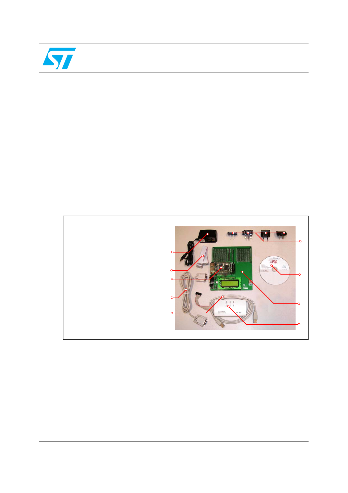
Figure 1. DK3400 Contents
UM0131
USER MANUAL
Turbo Plus uPSD DK3400 Development Kit
.
1. DK3400 Motherboard
2. ED3K4 uPSD3400 module
3. DK3400 CD
4. 110V/220V AC adapter
5. Plug adapters
6. RS232 Serial Cable
7. USB ULINK Adapter
8. USB Cables (x2, only 1 shown):
1 for ULINK, 1 for uPSD
9. 14-pin female-female ribbon
cable (JTAG)
10. Quick Start Flyer (not shown)
5
4
9
2
6
8
3
1
7
Rev 1
March 2005 UM0131 1/32
32
Page 2

Contents Turbo Plus uPSD DK3400 Development Kit
Contents
1 Introduction . . . . . . . . . . . . . . . . . . . . . . . . . . . . . . . . . . . . . . . . . . . . . . . . . . 1
2 DK3400 Hardware Features . . . . . . . . . . . . . . . . . . . . . . . . . . . . . . . . . . . . . 3
3 ED3K4 Hardware and Operation Mode . . . . . . . . . . . . . . . . . . . . . . . . . . . . 6
3.1 ED3K4 Hardware Architecture . . . . . . . . . . . . . . . . . . . . . . . . . . . . . . . . . . . . 6
3.1.1 ED3K4 Jumpers Diagram . . . . . . . . . . . . . . . . . . . . . . . . . . . . . . . . . . . . . . . . 7
3.1.2 Jumpers Description . . . . . . . . . . . . . . . . . . . . . . . . . . . . . . . . . . . . . . . . . . . . 8
3.1.3 Connector Description . . . . . . . . . . . . . . . . . . . . . . . . . . . . . . . . . . . . . . . . . . 10
3.1.4 ED3K4 Top connection capabilities . . . . . . . . . . . . . . . . . . . . . . . . . . . . . . . . 13
3.1.5 LEDs on ED3K4 . . . . . . . . . . . . . . . . . . . . . . . . . . . . . . . . . . . . . . . . . . . . . . 15
3.2 ED3K4 Operation Mode . . . . . . . . . . . . . . . . . . . . . . . . . . . . . . . . . . . . . . . . 15
3.2.1 Operation Mode 1: USB Mass Storage Mode . . . . . . . . . . . . . . . . . . . . . . . . 15
3.2.2 Operation Mode 2: uPSD+E-RLINK Mode . . . . . . . . . . . . . . . . . . . . . . . . . . 16
3.2.3 Operation Mode 3: Stand-alone RLINK mode . . . . . . . . . . . . . . . . . . . . . . . . 17
3.2.4 Operation Mode 4: uPSD+ULINK mode . . . . . . . . . . . . . . . . . . . . . . . . . . . . 18
3.2.5 Operation Mode 5: ED3K4+DK3400 Motherboard mode . . . . . . . . . . . . . . . 19
4 DK3400 Motherboard Hardware Architecture . . . . . . . . . . . . . . . . . . . . . . 20
4.1 Jumper description . . . . . . . . . . . . . . . . . . . . . . . . . . . . . . . . . . . . . . . . . . . . 20
4.2 Connector description . . . . . . . . . . . . . . . . . . . . . . . . . . . . . . . . . . . . . . . . . . 21
5 Getting Started With DK3400 . . . . . . . . . . . . . . . . . . . . . . . . . . . . . . . . . . . 22
Appendix A ED3K4 Schematic . . . . . . . . . . . . . . . . . . . . . . . . . . . . . . . . . . . . . . . 23
Appendix B DK3400 Motherboard Schematic . . . . . . . . . . . . . . . . . . . . . . . . . . . 30
6 Revision History . . . . . . . . . . . . . . . . . . . . . . . . . . . . . . . . . . . . . . . . . . . . . 31
2/32 UM0131
Page 3

Turbo Plus uPSD DK3400 Development Kit DK3400 Hardware Features
2 DK3400 Hardware Features
The DK3400 comprises both the ED3K4 board and DK3400 motherboard. ED3K4 is able to
work as an uPSD3400 module independently or work together with DK3400 motherboard. The
DK3400 motherboard works as a base board for the ED3K4. It is possible to upgrade the
motherboard with extension boards (for example, ED3K3 and DKMMX which are currently in
development).
The DK3400 motherboard itself has a variety of hardware capabilities built-in. A number of
hardware features on the DK3400 are provided to enable exploration by the user and for future
demo application software, including (see Figure 2 and Figure 3):
● Two selectable power sources of ED3K4: USB cable and 5V wall adapter
● Dual USB port for E-RLINK and uPSD USB users respectively
● Total of 100 pins for extension connector
● One JTAG port
● One RS232 connector
● One small regulated 5V power jack on ED3K4 and one 9V power jack on the DK3400
motherboard
● 128 Mbit NAND Flash
● Very small QFN package RTC from STMicroelectronics
● 8 Mbit SPI interface Flash
● 16 Kbit I2C interface EEPROM
● Embedded debug tools RLINK
● IrDA transceiver
● 122*32 Dot Matrix LCD with Chinese font support
● PS/2 standard keyboard connector
UM0131 3/32
Page 4
DK3400 Hardware Features Turbo Plus uPSD DK3400 Development Kit
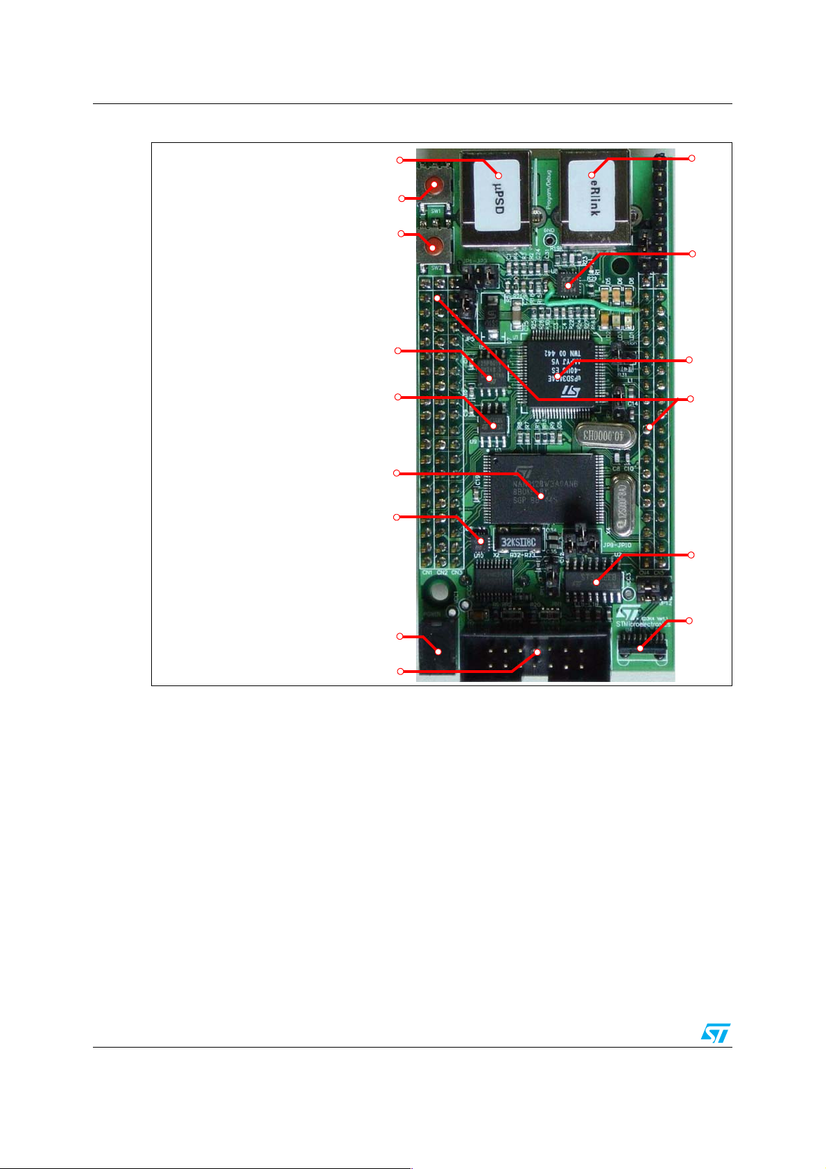
Figure 2. ED3K4 Board Features
1. USB port for E-RLINK
2. USB port for uPSD user
3. Power-on Switch
4. Reset Switch
5. 5V power jack
6. 14-pin JTAG Connector
7. uPSD34XX
8. Expansion Connectors
9. IrDA Transceiver
10. NAND flash
11. Real-Time Clock
12. I2C interface EEPROM
13. SPI interface Flash
14. RS232 transceiver
15. Power management
13
12
10
11
2
1
4
3
15
7
8
14
9
5
6
4/32 UM0131
Page 5
Turbo Plus uPSD DK3400 Development Kit DK3400 Hardware Features
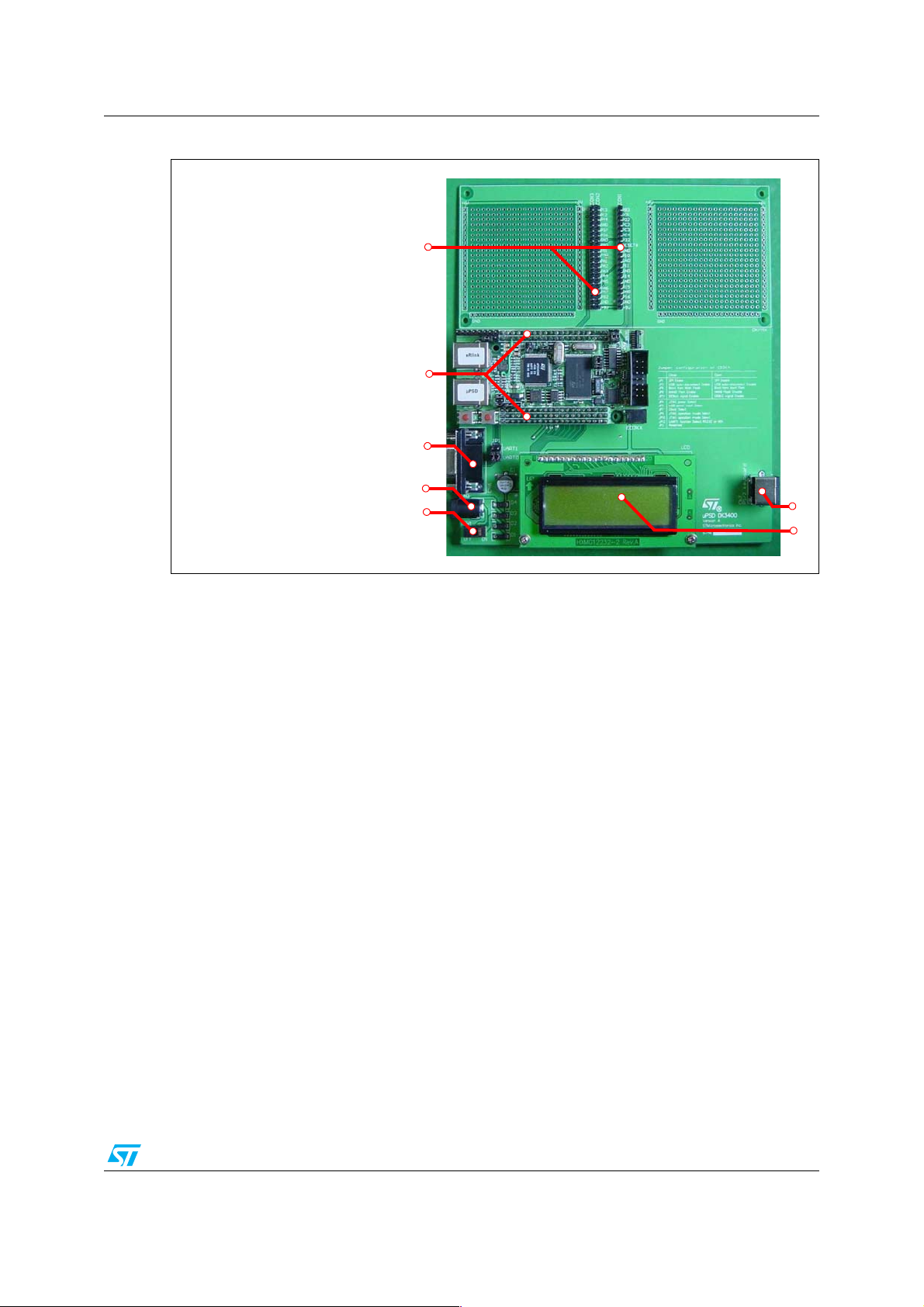
Figure 3. DK3400 Motherboard Features
7
1. Power Switch
2. 9V Power Input
3. Dot Matrix LCD
4. RS232 connector
5. PS/2 connector
6. Connectors for ED3Kx
7. Connectors for DKMMX
6
4
2
1
5
3
UM0131 5/32
Page 6

ED3K4 Hardware and Operation Mode Turbo Plus uPSD DK3400 Development Kit
3 ED3K4 Hardware and Operation Mode
The ED3K4 is a very low cost uPSD3400 evaluation module with full-speed USB support,
embedded debug tools RLINK and 128-Mbit NAND flash. Depending on different application
purposes, ED3K4 can be configured to one of the following 5 operation modes:
● Mode1: USB mass storage mode
● Mode2: uPSD3400+E-RLINK mode
● Mode3: Stand-alone RLINK mode
● Mode4: uPSD3400+ULINK mode
● Mode5: ED3K4+DK3400 motherboard mode
The 5 operation modes will be introduced in detail later.
3.1 ED3K4 Hardware Architecture
The jumpers and connectors definitions on ED3K4 board are detailed in this chapter.
6/32 UM0131
Page 7
Turbo Plus uPSD DK3400 Development Kit ED3K4 Hardware and Operation Mode
3.1.1 ED3K4 Jumpers Diagram
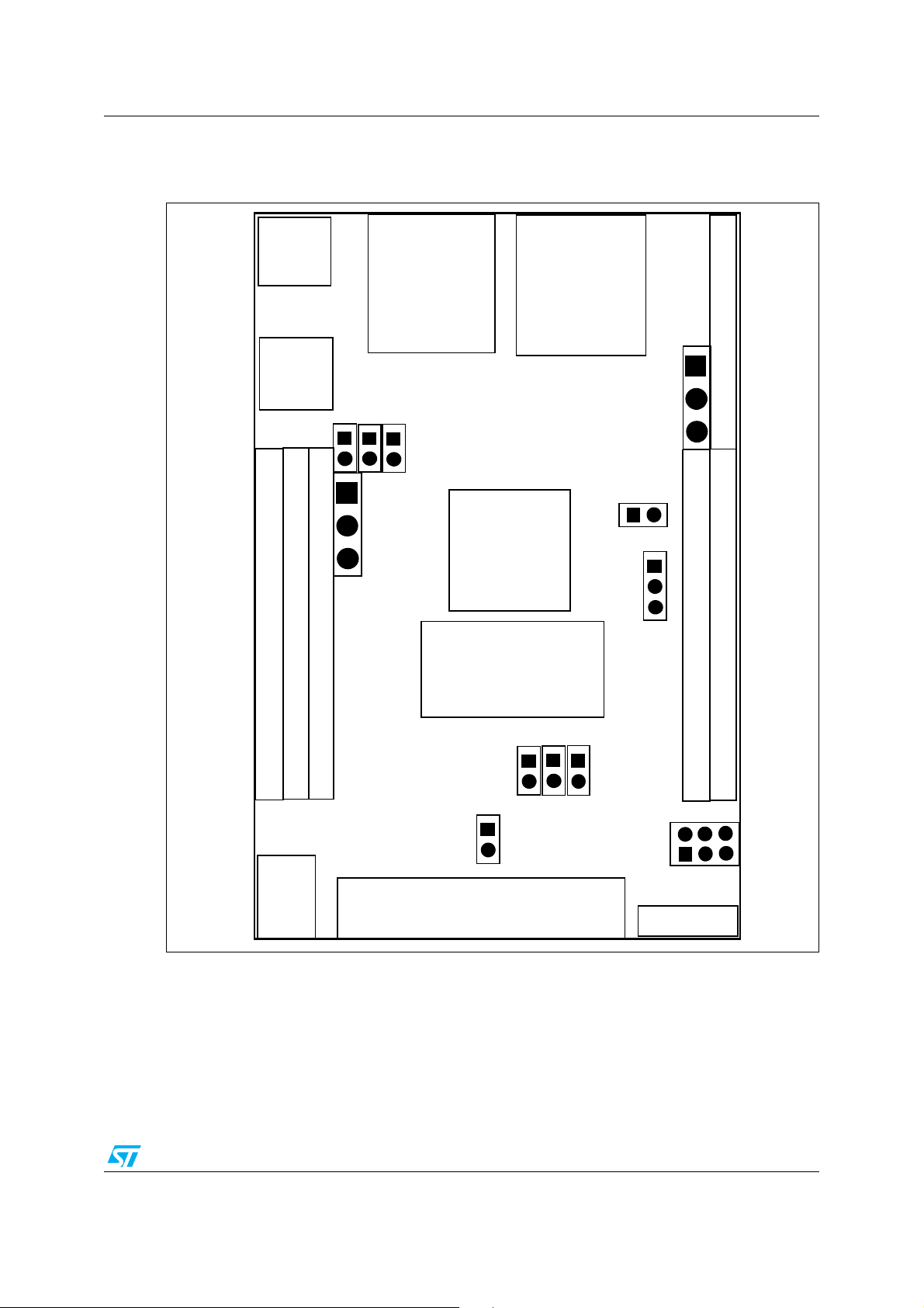
Figure 4. Block diagram layout of the jumper positions of the ED3K4 board
SW1
SW2
Extension connector CN1
Extension connector CN2
Extension connector CN3
JP1 JP2
1
2
3
JP5
uPSD
JP3
1
2
eRlink
uPSD3400
128Mbit NAND Flash
JP8 JP9 JP10
JP6
1 2
1
2
3
JP7
1
2
3
JP4
Extension connector CN4
Extension connector CN5
Power
1
2
JP11
1
2
JTAG connector
JP12
2 4 6
1 3 5
IrDA
UM0131 7/32
Page 8
ED3K4 Hardware and Operation Mode Turbo Plus uPSD DK3400 Development Kit
3.1.2 Jumpers Description
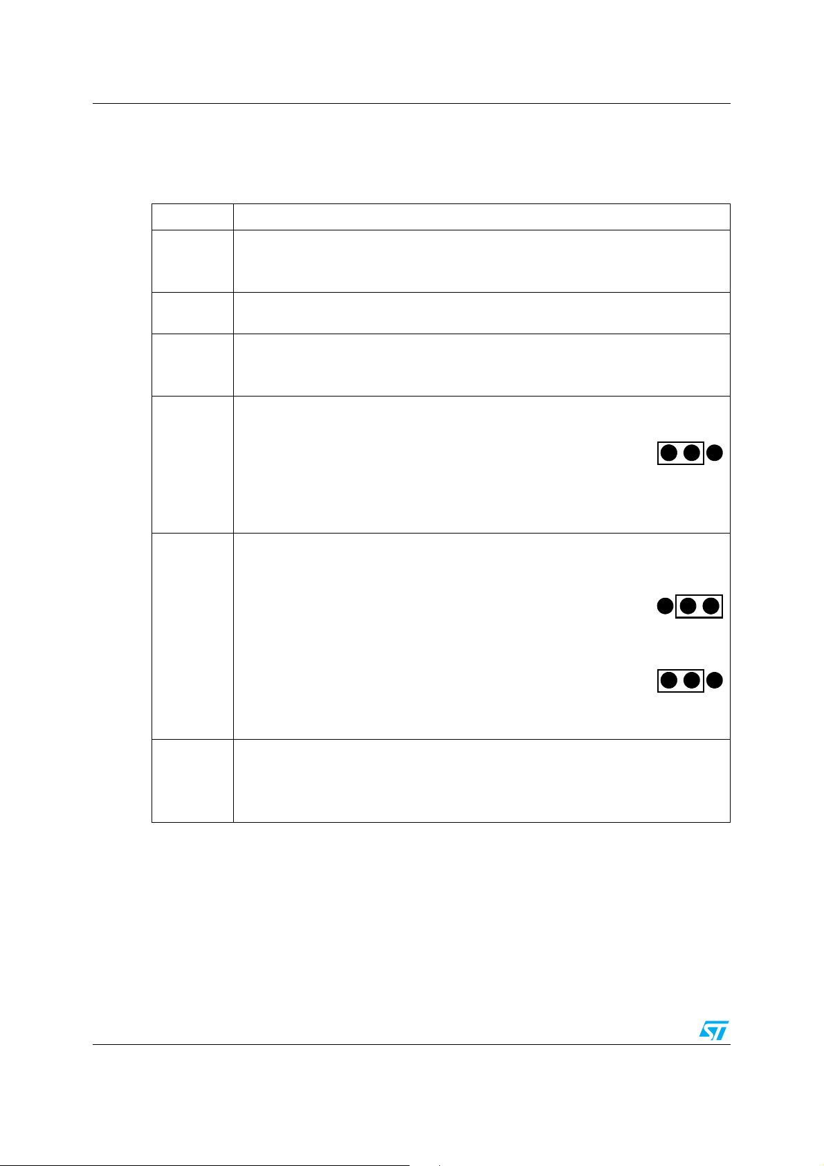
The definitions of the jumpers on ED3K4 board are listed in Ta b le 1 :
Table 1. Description of jumpers on ED3K4 board
Jumper Description
JP1 is used to enable SPI interface Flash M25P80.
JP1
JP2
JP3
M25P80 is enabled when JP1 is closed.
Default status: closed
Reserved. Please keep this jumper on open.
Default status: open
JP3 is used to enable USB auto-disconnect function.
USB auto-disconnect function is enabled when JP3 is closed.
Default status: closed
JP4 is used to select a power source for JTAG port.
Keep JP4 on following status when ED3K4 works on Mode1, 2, 4 and 5:
JP4
JP5
JP6
123
Keep JP4 on open when ED3K4 works on Mode 3.
Default status: JP4.1 connected to JP4.2
JP5 is used to select which power source will be used as USB power input of power
management circuit, power from E-RLINK USB cable or power from uPSD USB cable.
Keep JP5 on following status when ED3K4 powered from RLINK USB cable:
123
Keep JP5 on following status when ED3K4 powered from uPSD USB cable:
123
Default status: JP5.1 connected to JP5.2
JP6 is used to provide a boot option for ED3K4 board.
ED3K4 boot from internal main flash when JP6 is closed.
ED3K4 boot from internal boot flash when JP6 is open.
Default status: open
8/32 UM0131
Page 9
Turbo Plus uPSD DK3400 Development Kit ED3K4 Hardware and Operation Mode
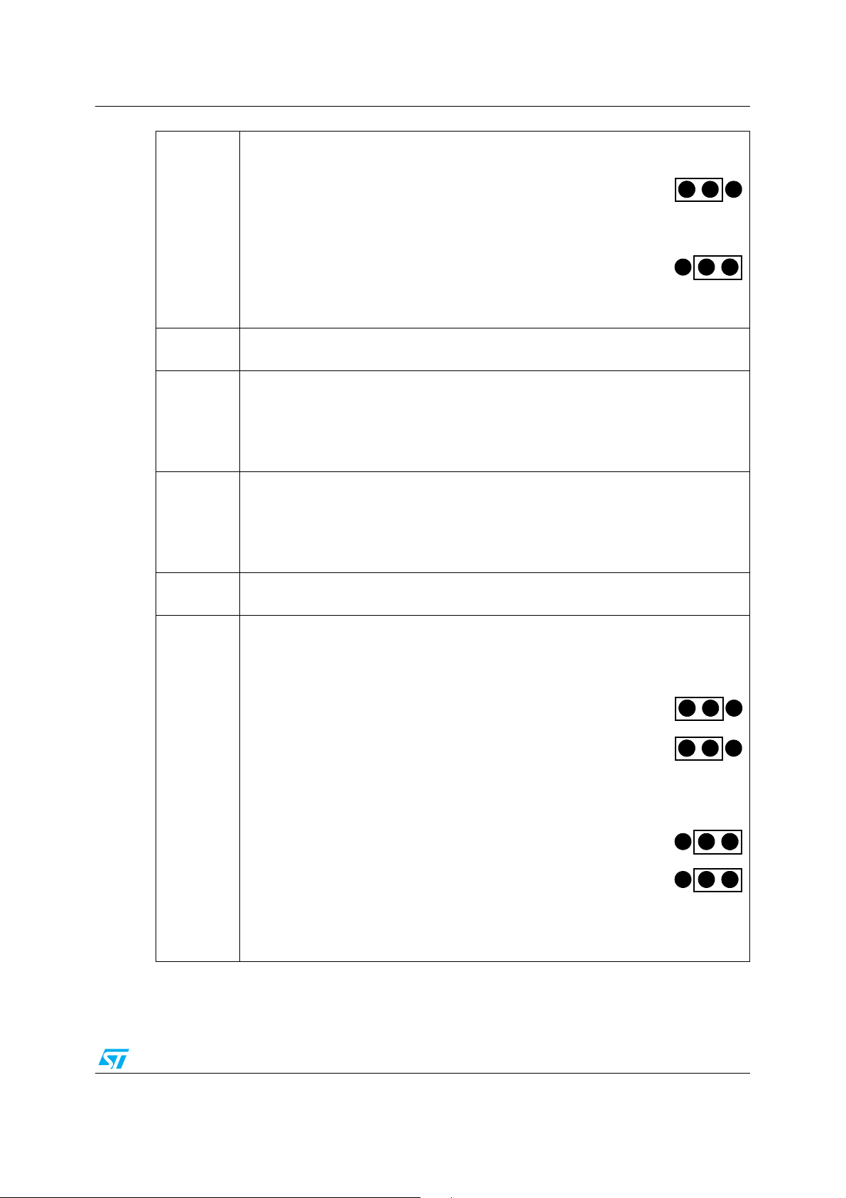
JP7 is used to select clock generation source, external clock or internal clock.
ED3K4 works with internal clock when JP7 is set as following:
123
JP7
JP8
JP9
JP10
JP11
ED3K4 works on external clock mode when JP4 is set as following:
123
Default status: JP7.1 connected to JP7.2
JP8 is used to enable NAND Flash. 128Mbit NAND flash is enabled when JP8 is closed.
Default status: closed
JP9 is used to select JTAG circuit operation mode along with JP10 depending on
operation mode of ED3K4.
Keeps JP9 on closed when ED3K4 works on mode 1, 2, 3 and 5.
Keeps JP9 on open when ED3K4 works on mode 4.
Default status: closed
JP10 is used to select JTAG circuit operation mode along with JP9 depending on
operation mode of ED3K4.
Keeps JP10 on closed when ED3K4 works on mode 1, 2, 4 and 5.
Keeps JP10 on open when ED3K4 works on mode 3.
Default status: closed
JP11 is used to enable DEBUG signal. DEBUG signal is enabled when JP11 is closed.
Default status: open
JP12 is used to select which transceiver will be connected to UART1 port,
RS232 transceiver or IrDA transceiver.
UART1 is connected to RS232 transceiver when JP12 is set as following:
246
JP12
135
UART1 is connected to IrDA transceiver when JP12 is set as following:
246
135
Default status JP12.2 connected to JP12.4;
Default status JP12.1 connected to JP12.3.
UM0131 9/32
Page 10

ED3K4 Hardware and Operation Mode Turbo Plus uPSD DK3400 Development Kit
3.1.3 Connector Description
The definitions of connectors on ED3K4 board are listed in Ta b le 2 and Ta bl e 3:
Table 2. Description of connectors on ED3K4 board
Connector Description
POWER
USER USB USB port connected to uPSD3400 on board.
E-RLINK USB USB port for embedded RLINK
JTAG JTAG port used for debugging and programming
CN1, 2, 3, 4 and 5 100 pins Extension connectors for user.
Regulated 5V power jack.
Note: The absolute Maximum voltage on this jack is 6V.
10/32 UM0131
Page 11

Turbo Plus uPSD DK3400 Development Kit ED3K4 Hardware and Operation Mode
Table 3. Description of the 100-pin extension connector CN1,2,3,4 and 5
Connector Signal Name Pins Description
RD# 1 READ signal
WR# 2 WRITE signal
3,4,5,6,7,8
9,10,11
Ground
GPIO/PLD Output or Input/SRAM standby
voltage input(Vstby)
External 5V wall adapter power source (56V)
CN1
CN2
GND
MCU_AD0 12 Multiplexed Address/Data bus A0/D0
MCU_AD1 13 Multiplexed Address/Data bus A1/D1
MCU_AD2 14 Multiplexed Address/Data bus A2/D2
MCU_AD3 15 Multiplexed Address/Data bus A3/D3
MCU_AD4 16 Multiplexed Address/Data bus A4/D4
MCU_AD5 17 Multiplexed Address/Data bus A5/D5
MCU_AD6 18 Multiplexed Address/Data bus A6/D6
MCU_AD7 19 Multiplexed Address/Data bus A7/D7
PSEN# 20 PSEN signal external bus
PC2/VSTBY 1
GND 2,19 Ground
VCC1 3,4,5,6,7,8
PA7 9 GPIO on port A
PA6 10 GPIO on port A
PA5 11 GPIO on port A
PA4 12 GPIO on port A
PWR_DOWN 13,17 Reserved
PA3 14 GPIO on port A
PA2 15 GPIO on port A
P34/C0 16 GPIO/Counter 0 input
VBATT 18 Reserved
EXT_CLK 20 External clock input
UM0131 11/32
Page 12

ED3K4 Hardware and Operation Mode Turbo Plus uPSD DK3400 Development Kit
PC3/TSTAT 1 GPIO/optional JTAG status(TSTAT)
MCU_SPI_SEL 2 SPI slave select signal
MCU_SPI_TXD 3 SPI TXD signal
MCU_SPI_RXD 4 SPI RXD signal
MCU_SPI_CLK 5 SPI clock signal output
P42/TCM2 6 GPIO/PCA0-TCM2/UART1 RXD signal
P41/TCM1 7 GPIO/PCA0-TCM1/Timer 2 trigger input
P40/TCM0 8 GPIO/PCA0-TCM0/Timer 2 counter input
P32/INT0 9 GPIO/External interrupt0 input
CN3
CN4
P33/INT1 10 GPIO/External interrupt1 input
P11/T2X 11 GPIO/Timer 2 trigger input/ADC channel 1
GND 12,17 Ground
TXD1_232 13 UART1 TXD signal on RS232 voltage level
RXD1_232 14 UART1 RXD signal on RS232 voltage level
PA1 15 GPIO on port A
PA0 16 GPIO on port A
P36/SDA 18 GPIO/I2C Bus serial data
P37/SCL 19 GPIO/I2C Bus clock
VCC3 20 3.3V power
CPU_DEBUG 1 I/O to the MCU Debug Unit
PC7 2 GPIO/PLD input and output
PD1 3 GPIO/PLD IO
PB0 4 GPIO/PLD IO/Address Latch output
P31/TXD0 5 GPIO/UART0 transmit TXD signal
P30/RXD0 6 GPIO/UART0 receive RXD signal
GND
TXD0_232 8 UART0 TXD signal on RS232 voltage level
RXD0_232 9 UART0 TXD signal on RS232 voltage level
PC4/TERR# 10 GPIO/Optional JTAG status(TERR)
P35/C1 11 GPIO/Counter1 input
VCC2 12 5V power
P17/AD7 14 GPIO/SPI slave select/ADC channel 7
P15/AD5 16 GPIO/SPI receive/ADC channel 5
P13/AD3 18
RESET# 20 System reset signal
7,13,15,17
19
Ground
GPIO/UART1 or IrDA transmit/ADC
channel 3
12/32 UM0131
Page 13

Turbo Plus uPSD DK3400 Development Kit ED3K4 Hardware and Operation Mode
ALE 1 Address latch signal
PD2 2 GPIO/PLD input and output
PB0 13 GPIO/PLD IO/Address Latch output
PB1 3,12 GPIO/PLD IO/Address Latch output
PB2 4,11 GPIO/PLD IO/Address Latch output
PB3 5,10 GPIO/PLD IO/Address Latch output
PB4 6 GPIO/PLD IO/Address Latch output
PB5 7 GPIO/PLD IO/Address Latch output
CN5
PB6 8 GPIO/PLD IO/Address Latch output
PB7 9 GPIO/PLD IO/Address Latch output
VCC2 14 5V power
P16/ADC6 15 GPIO/SPI transmit/ADC channel 6
VCC3 16,18 3.3V power
P14/ADC4 17 GPIO/SPI clock output/ADC channel 4
P12/ADC2 19
P10/ADC0 20
GPIO/UART1 or IrDA receive/ADC channel
2
GPIO/Timer 2 counter input/ADC channel
0
3.1.4 ED3K4 Top connection capabilities
Various external connectivity is provided based on 100-pin connector on ED3K4, including 7
channels of ADC, 6 channels of PWM/SERVO output, 3 channels of Timing capture, SRAM
backup power input, UART1 RS232 level, UART0 digital level, POWER-DOWN input, External
battery, External clock, I2C and External RESET. All possible top connection capabilities have
been listed in following Tab le 4.
Table 4. ED3K4 Top connection capabilities
Capabilities Signals name Headers
SRAM backup power
PWM/SERVO OUTPUT1
PWM/SERVO OUTPUT2
PWM/SERVO OUTPUT3
PWM/SERVO OUTPUT4
PC2/VSTBY CON2.1
GND CON2.2
GND CON1.3
VCC1 CON2.3
MCU_SPI_TXD CON3.3
GND CON1.4
VCC1 CON2.4
MCU_SPI_RXD CON3.4
GND CON1.5
VCC1 CON2.5
MCU_SPI_CLK CON3.5
GND CON1.6
VCC1 CON2.6
P42/TCM2 CON3.6
UM0131 13/32
Page 14

ED3K4 Hardware and Operation Mode Turbo Plus uPSD DK3400 Development Kit
GND CON1.7
PWM/SERVO OUTPUT5
PWM/SERVO OUTPUT6
TIMING CAPTURE 1
TIMING CAPTURE 2
TIMING CAPTURE 3
UART1 RS232 level
POWER-DOWN
EXTERNAL BATTERY CONNECTION
EXTERNAL CLOCK INPUT
I2C BUS WITH GND+POWER
UART0 DIGITAL LEVEL
ADC channel 1
ADC channel 2
ADC channel 3
ADC channel 4
ADC channel 5
ADC channel 6
VCC1 CON2.7
P41/TCM1 CON3.7
GND CON1.8
VCC1 CON2.8
P40/TCM0 CON3.8
GND CON1.9
PA 7 C ON 2. 9
P32/INT0 CON3.9
GND CON1.10
PA6 CON2.10
P33/INT1 CON3.10
GND CON1.11
PA5 CON2.11
P11/T2X CON3.11
TXD1_232 CON3.13
RXD1_232 CON3.14
PWR_DOWN CON2.17
GND CON3.17
VBATT CON2.18
GND CON2.19
EXT_CLK CON2.20
GND CON2.19
GND CON3.17
P36/SDA CON3.18
P37/SCL CON3.19
VCC3 CON3.20
P31/TXD0 CON4.5
P30/RXD0 CON4.6
GND CON4.7
P11/T2X CON3.11
GND CON3.12
P12/ADC2 CON5.19
GND CON4.19
P13/ADC3 CON4.18
GND CON4.19
P14/ADC4 CON5.17
GND CON4.17
P15/ADC5 CON4.16
GND CON4.17
P16/ADC6 CON5.15
GND CON4.15
14/32 UM0131
Page 15

Turbo Plus uPSD DK3400 Development Kit ED3K4 Hardware and Operation Mode
ADC channel 7
EXTERNAL RESET
3.1.5 LEDs on ED3K4
There are 7 LEDs to indicate the work status on ED3K4 board. D5 and D8 are driven by Power
management chips. LD1, LD2 and LD3 are used to indicate the work status of the embedded
Rlink. D2 is used to indicate the JTAG operation. D6 is a user LED that can be driven by uPSD
PD1. All the LEDs D5, D6, D8, LD1, LD2 and LD3 are located on the area near by the eRlink
USB port. D2 is located on the area near the POWER connector. Please find the detailed
information in Ta bl e 5 .
Table 5. LED description
LED Color Usage
D2 red JTAG operation indicator LED
D5 red Power indicator LED
D8 red Low battery indicator LED
LD1 green eRlink Power indicator LED
LD2 red eRlink BUSY indicator LED
LD3 green eRlink RUN indicator LED
D6 red User LED that can be driven by uPSD3434E on board
P17/ADC7 CON4.14
GND CON4.13
RESET# CON4.20
GND CON4.19
3.2 ED3K4 Operation Mode
The ED3K4 is a versatile uPSD3400 module with 5 user operation modes. You may treat it as a
uPSD3400 user target board, standalone debug tools RLINK or an integrated uPSD3400
development platform with embedded SW evaluation capability depending on the relative
configuration and usage. The 5 operation modes will be introduced in the following chapter one
by one.
3.2.1 Operation Mode 1: USB Mass Storage Mode
The ED3K4 module may be used as a low speed USB device with file storage function on
operation mode1. Connected to PC with WinXP via a USB cable, it can be used to download
and upload files to or from the ED3K4 module.
UM0131 15/32
Page 16

ED3K4 Hardware and Operation Mode Turbo Plus uPSD DK3400 Development Kit
Figure 5. ED3K4 operation mode 1 connection
-A
PC HOST
(2x)
eRlink
3400
uPSD
TOP SIDE
-A
USB-B
Hardware connection on Mode 1
Please refer to Figure 5 for the connection on operation mode 1.
Configuration of jumpers on Mode 1
Please refer to Ta bl e 6 for detailed information about jumper configuration on operation mode 1.
Table 6. Jumper configuration on Mode 1
Jumper Status Jumper Status Jumper Status
JP1 closed JP5 1<->2 JP9 closed
JP2 open JP6 closed JP10 closed
JP3 closed JP7 1<->2 JP11 open
JP4 1<->2 JP8 closed JP12 1<->3;2<->4
3.2.2 Operation Mode 2: uPSD+E-RLINK Mode
NAND
JTAG
The ED3K4 module may be used as integrated uPSD3400 development platform with
embedded RLINK on operation mode2. You can build the small uPSD3400 platform by simply
connecting the ED3K4 to a PC with RIDE via a USB cable.
Figure 6. ED3K4 operation mode 2 connection
-A
PC HOST
debug
(2x)
eRlink
3400
uPSD
TOP SIDE
-A
user
USB-B
16/32 UM0131
NAND
JTAG
Page 17

Turbo Plus uPSD DK3400 Development Kit ED3K4 Hardware and Operation Mode
Hardware connection on Mode 2
Please refer to Figure 6 for the connection on operation mode 2.
Configuration of jumpers on Mode 2
Please refer to Ta bl e 7 for detailed information about jumper configuration on operation mode 2.
Table 7. Jumper configuration on Mode 2
Jumper Status Jumper Status Jumper Status
JP1 closed JP5 2<->3 JP9 closed
JP2 open JP6 closed JP10 closed
JP3 closed JP7 1<->2 JP11 open
JP4 1<->2 JP8 closed JP12 1<->3;2<->4
3.2.3 Operation Mode 3: Stand-alone RLINK mode
The ED3K4 module may be used as a stand-alone uPSD debug tool like RLINK on operation
mode3. Only the embedded RLINK is active on ED3K4 board on this operation mode.
Figure 7. ED3K4 operation mode 3 connection
-A
PC HOST
-A
debug
USB-B
(2x)
eRlink
uPSD
NAND
3400
ED3K4
uPSD
JTAG
Standard
14-pin cable
JTAG
uPSD Target Board
Hardware connection on Mode 3
Please refer to Figure 7 for the connection on operation mode 3.
Configuration of jumpers on Mode 3
Please refer to Ta bl e 8 for detailed information about jumper configuration on operation mode 3.
Table 8. Jumper configuration on Mode 3
Jumper Status Jumper Status Jumper Status
JP1 closed JP5 1<->2 JP9 closed
UM0131 17/32
Page 18

ED3K4 Hardware and Operation Mode Turbo Plus uPSD DK3400 Development Kit
JP2 open JP6 closed JP10 open
JP3 closed JP7 1<->2 JP11 open
JP4 open JP8 closed JP12 1<->3;2<->4
3.2.4 Operation Mode 4: uPSD+ULINK mode
The ED3K4 module may be treated as a uPSD target board on operation mode4. The
embedded RLINK on board is disabled in this mode. You may connect ED3K4 with another
JTAG-based uPSD debug tools like ULINK from Keil in this mode.
Figure 8. ED3K4 operation mode 4 connection
-A
PC HOST
-A
user
eRlink
uPSD
NAND
3400
JTAG
USB-B
(2x)
debug
ED3K4
JTAG
Standard
14-pin cable
ULINK
Hardware connection on Mode 4
Please refer to Figure 8 for the connection on operation mode 4.
Configuration of jumpers on Mode 4
Please refer to Table 9 for detailed information about jumper configuration on operation mode
4.
Table 9. Jumper configuration on Mode 4
Jumper Status Jumper Status Jumper Status
JP1 closed JP5 1<->2 JP9 open
JP2 open JP6 closed JP10 closed
JP3 closed JP7 1<->2 JP11 open
JP4 1<->2 JP8 closed JP12 1<->3;2<->4
18/32 UM0131
Page 19

Turbo Plus uPSD DK3400 Development Kit ED3K4 Hardware and Operation Mode
3.2.5 Operation Mode 5: ED3K4+DK3400 Motherboard mode
The ED3K4 module is capable of working together with the DK3400 motherboard in operation
mode 5. The dot-matrix LCD, RS232 connector and PS/2 Keyboard are available for use in this
operation mode. The default DK3400 will be delivered with mode 5. You are allowed to program
and debug DK3400 using alternative JTAG debug tools, embedded Rlink or external ULINK on
mode 5. Please make sure that the jumper configuration of JP9 and JP10 is compatible with
requirement in mode 2 when you select eRlink as debug tools. Please also make sure that the
jumper configuration of JP9 and JP10 is compatible with requirement in mode 4 when you
select external ULINK as debug tools.
Hardware connection on Mode 5
Just plug ED3K4 module in the ED3Kx socket on DK3400 motherboard.
Configuration of jumpers on Mode 5
Please refer to Tab le 1 0 for detailed information about jumper configuration on operation mode
5.
Table 10. Jumper configuration on Mode 5
Jumper Status Jumper Status Jumper Status
JP1 closed JP5 open JP9 closed
JP2 open JP6 open JP10 closed
JP3 closed JP7 1<->2 JP11 open
JP4 1<->2 JP8 closed JP12 1<->3;2<->4
UM0131 19/32
Page 20

DK3400 Motherboard Hardware Architecture Turbo Plus uPSD DK3400 Development Kit
4 DK3400 Motherboard Hardware Architecture
The DK3400 motherboard can be used as a base board for both the uPSD module ED3K4 and
ED3K3. The power supply, LCD, RS232 interface and PS/2 Keyboard interface are available on
this board.
4.1 Jumper description
The jumper definitions on the DK3400 motherboard are listed in Tab l e 11 .
Table 11. Description of jumpers on DK3400 motherboard
Jumper Description
JP1 is used to select which UART port is connected to RS232 connector on DK3400
motherboard.
UART0 is connected to RS232 connector when JP1 is set as following:
246
JP1
135
UART1 is connected to RS232 connector when JP1 is set as following:
246
135
Default status:
JP1.3 connected to JP1.5;
JP1.4connected to JP1.6.
20/32 UM0131
Page 21

Turbo Plus uPSD DK3400 Development Kit DK3400 Motherboard Hardware Architecture
4.2 Connector description
The connector definitions on the DK3400 motherboard are listed in Ta bl e 12 .
Table 12. Description of connectors on DK3400 motherboard
Connector Description
CN0 9V power jack.
CN1,2,3,4 and 5 Connectors for ED3Kx module
CN6 RS232 connector (female)
CN7 PS/2 standard Keyboard connector
DKMMX_CON1 Connector for DKMMX board
DKMMX_CON2 Connector for DKMMX board
DKMMX_CON3 Connector for DKMMX board
UM0131 21/32
Page 22

Getting Started With DK3400 Turbo Plus uPSD DK3400 Development Kit
5 Getting Started With DK3400
The DK3400 is delivered in default operation mode 5 with the RTC demonstration application.
Please follow the steps below to get started using the DK3400:
Check with Jumper configuration
Please check the jumper configuration to guarantee that all jumper status are the same as
those listed in Ta bl e 1 0 (ED3K4 operation mode 5).
Connecting DK3400 board for RTC demo
1. Connect the AC adapter to the DK3400 board. The DK3400 AC adapter will work on either
110V or 220V, and contains several different plug adapters to fit popular European AC
outlets. Please set up your AC adapter to fit your AC plug type and plug in the AC adapter.
Then plug the small power plug into the DK3400 9V DC input.
2. Connect a PS/2 standard Keyboard to PS/2 connector on DK3400 motherboard.
Step 3 - Try Your DK3400 Board with RTC demo.
Turn DK3400 on. Your DK3400 board will boot from RTC demo application.
You should see the DK3400 RTC demo running in the LCD window. The RTC time can be
updated by pressing keys “up”, “down”, “left”, “right” and “enter” on the Keyboard.
Additional Information
The uPSD3400 series design guide application notes for DK3400 using RIDE or KEIL's
software tools are available for download from the ST website:
http://www.st.com/psm
22/32 UM0131
Page 23

Turbo Plus uPSD DK3400 Development Kit Getting Started With DK3400
Appendix A ED3K4 Schematic
D
C
B
A
1.1
432
ED3K4
Number RevisionSize
A4
Title
Date: 2 3-Feb-2005
SCH
RLINK
Power
Power.
SCH
IO
IO.
1
D
RLINK.SCH
SCH
JTAG
JTAG.SCH
U.SCH
MC U
MC
C
Peripherals
Peripherals.
B
A
2 3 4
1
UM0131 23/32
Page 24

Getting Started With DK3400 Turbo Plus uPSD DK3400 Development Kit
D
C
B
A
1.1
4321
12345678910111213141516171819
CN5
ALE
PD2
PB1
PB2
PB3
PB4
PB5
PB6
PB7
12345678910111213141516171819
CN4
CPU_DEBUG
PC7
PD1
PB0
P31/TXD0
P30/RXD0
TXD0_232
RXD0_232
GND
12345678910111213141516171819
CN3
ADC6
VCC2
P16/
C1
PC4/TERR#
P35/
GND
VCC2
GND
P17/ADC7
VCC3
P15/ADC5
P14/ADC4
GND
VCC3
P13/ADC3
P12/ADC2
GND
20
CON20
ADC0
P10/
CONNECTOR
Number RevisionSize
A4
Title
20
CON20
R1
RESET#
20
CON20
1k5
5V_RLINK
Date: 23-Feb-2005
0
TCM
P42/TCM 2
VCC1
GND
P41/TCM 1
VCC1
GND
P40/
VCC1
GND
P32/INT0
PA7
GND
P33/INT1
PA6
GND
T2X
P11/
PA5
GND
GND
PA4
U_AD0MCU_AD1
MC
TXD1_232
RXD1_232
R_DOWN
PW
PA3
MC U_AD2
PA1
PA2
U_AD3
MC
PC3/TSTAT
MCU_ SPI_CLK
MC U_SPI_TXD
MC U_SPI_RXD
MCU_ SPI_SEL
12345678910111213141516171819
CN2
PC2/VSTBY
GND
VCC1
VCC1
VCC1
12345678910111213141516171819
CN1
RD#
WR#
GND
GND
GND
RLINK_USBD-
RLINK_USBD+
1D-2D+3
4
VCC
R2
1D-2D+3
VCC
U_USBD-
MC
22R322
6
GND
SHELL5SHELL
U_USBD+
MC
4
6
GND
SHELL5SHELL
31
VCC3
R34
5V_UDI SK
B
USB-
1
2
JP3
PC7
510
R4
R5
1K
T1
9013
10K
R35
36K
2
1 2 3 4
PA0
VCC3
P36/SDA
P37/SCL
GND
20
CON20
R_DOWN
GND
P34/C0
EXT_CLK
PW
VBATT
5V_UDISK
20
CON20
U_AD5MCU_AD6
MC U_AD4
MC
MC U_AD7
PSEN#
5V_RLINK
Program/Debug
C1
104
B
User USB
USB-
D
C
24/32 UM0131
B
A
Page 25

Turbo Plus uPSD DK3400 Development Kit Getting Started With DK3400
D
C
B
A
1.1
4321
RR2
10K
VCC2
6
7
8
6
7
8
4 5
3
2
1
RR1
10K
4 5
3
2
1
JTAG_VCC
C2
104
1
3
5
7
9
11
13
TDI
JEN
VCC
TM S
TCK
TDO
GND
TRST
CNTL
TSTAT
RST
GND
GND
TERR
JTAG
14
2
4
6
8
10
12
RED
D2
VCC2
JTAG_CNTL
RLINK_TRST
RLINK_CNTL
RLINK_JEN
JTAG
Number RevisionSize
A4
Title
Date: 2 3-Feb-2005
R6
470
CPU_DEBUG
1
BAT54S
JP4
12233
TDI
PC0/TM S
PC1/TCK
PC5/
RESET#
RLINK_TDO
RLINK_TSTAT
RLINK_TERR
1Y1181Y2161Y3141Y4
0
2
JTAG_VCC
1A121A241A361A4
U10
PC3/TSTAT
PC4/TERR#
D
C
3
9
12
2Y352Y272Y1
2Y4
VCC
8
TDO
GND
PC6/
GND
10
1 E
2 E
2A4172A3152A2132A1
74VHC244T
1
19
11
RLINK_RST
RLINK_TM S
RLINK_TCK
RLINK_TDI
1
2
JP10
JTAG_VCC
R33
1
2
JP9
B
VCC2
5V_RLINK
JTAG_VCC
4K7
4K7
R32
1 2 3 4
A
UM0131 25/32
Page 26

Getting Started With DK3400 Turbo Plus uPSD DK3400 Development Kit
D
C
B
A
1.1
4321
2uH
L1
2.
20pf
C14
103
123
JP7
CON3
EXT_CLK
VCC2
MC U_X1
R31
4K7
CSTCW-X
RESET#
Reset button
4 3
5
1 2
SW1
Delete RC reset circuit
1
2
JP6
BOOT Option
GND
PB3
Title
MCU
Number RevisionSize
A4
Date: 23 -Feb-2005
VCC3
VCC2
VCC2
20pf
X3
40MHZ
13
GND
X1
U_X2
MC
C10
2
C8
104
C4
104
C3
104
C5
MC U_AD1
MC U_AD0
36
P0.1/AD137P0.2/AD238P0.3/AD339P0.4/AD441P0.5/AD543P0.6/AD645P0.7/AD7
P0.0/AD0
uPSD3400-80
X1
U1
48X249
MC U_X1
S
VSTBY
U_AD7
MC U_AD2
MC U_AD3
MC U_AD4
MC U_AD5
MC U_AD6
MC
47
53
57
P2.0/A851P2.1/A9
P2.2/A1055P2.3/A11
RESET_I N
DEBUG
8
68
U_X2
RESET#
MC
P30/RXD0
CPU_DEBUG
JTAG_CNTL
1
2
JP11
RXD/P3. 075TXD/P3. 177EXINT0/ GATE0/P3. 279EXINT1/ GATE1/P3. 3
P32/INT0
P31/TXD0
PSEN#
ALE
RD#
PA0
PA1
PA2
PA3
PA4
PA5
PA6
PA7
PB0
PB1
PB2
PB4
PB5
PB6
64
ADC7
P17/
PB7
66
AVC C
AGND+P SDGND
Vref
72
70
69
GND
AVC C
WR#
65
62
63
4
ALE(PD0)
CTRL1/ RD
CTRL0/ WR
CTRL2/ PSEN
I2CSDA/P3.6
T0/P3.4
I2CSCL/ P3.7
T1/P3.5
2
44
46
40
42
C1
P33/INT1
P34/C0
P35/
P36/SDA
P37/SCL
32
PA035PA328PA426PA5
PA134PA2
ADC0
P10/
22
24
21
PB080PB178PB276PB374PB473PB571PB667PB7
PA6
PA7
ADC0/ T2/ P1.052ADC1/ T2x/ P1.154ADC 2/RXD2/ P1.256ADC 3/TXD2/ P1.358ADC4/ SPISCLK/ P1.459ADC 5/SPIRXD/P1. 560ADC 6/SPITXD/P1. 661ADC7/ SPISSEL/P1.7
ADC2
P13/ADC3
P14/ADC4
P15/ADC5
P16/ADC6
P11/T2X
P12/
TERR#
PD1
PD2
PC6/TDO
PC5/TDI
PC1/TCK
PC0/TM
20
17
TM S/PC0
33
2
P40/TCM 0
P41/TCM 1
P42/TCM
PC3/TSTAT
PC2/
15
16
TCK/ PC1
Vstby/ PC2
R_DOWN
M CU_SPI_CL K
PW
PC7
PC4/
9
7
6
5
3
1
PC7
PD1
TDI/ PC5
TDO/PC6
TSTAT/PC3
TERR / VBATON/ PC4
SPISSEL/ PCA1/ P4.718SPITXD/ TCM 5/P4.619SPIRXD/ TCM 4/P4.523SPISCLK/ TCM 3/P4.425TXD2/ PCA0/ P4.327RXD2/ TCM 2/P4.230T2x/ TCM 1/P4.131T2/TCM 0/ P4.0
L
MC U_SPI_TXD
MC U_SPI_RXD
M CU_SPI_SE
U_USBD+
PD2
MC U_USBD-
MC
USB-
4
1
USB+
1
1
GND
9
2
GND
3
1
VDD
5
0
VDD
1
2
VCC
0
1
VCC3
VCC2
1 2 3 4
D
C
26/32 UM0131
B
A
Page 27

Turbo Plus uPSD DK3400 Development Kit Getting Started With DK3400
4321
VCC3
VCC3
VCC3
RS232, IrDA
1Gbit NAND Flash
D
C
B
A
1.1
105
C16
T1out
T1i n
IO643IO5
RXD0_232
13
12
P30/RXD0
P14/ADC4
P15/ADC5
42
41NC40NC39NC38
R1in
R1out
IO4
TXD1_232
7
T2out
T2i n
10
VCC3
RXD1_232
8
R2in
R2out
9
37
36NC35NC34NC33
Vss
Vcc
15
GND
V-
ST3232
6
C18
105
T
6
SW2-SPD
4
P13/ADC3
P13/ADC3
P12/ADC2
31
IO332IO2
152
JP12
ADC0
P11/T2X
P10/
30
29NC28NC27NC26NC25
IO1
IO0
3
P12/ADC2
TXD0_232
14
4
5
16
C2-
C2+
VCC
C1+
V+
2
105
104
1
C17
48NC47NC46NC45
NC
C1-
3
11
105
P31/TXD0
P16/ADC6
P17/ADC7
44
IO7
U2
C15
C12
TxD
RxD
SD
U4
5
3
4
IrDA Interface Circuit (disable shutdown)
+
C7
D9
1N4148
I2C interface RTC and EEPROM
VCC3
X2
GND
Anode (VCC2)1Cathode
VCC16Vlogic
TFDU4300
8
2
7
C23
R11
5
R12
VCC3
22F
0.
41T6X
U6
M
1
4
C35
6pf
C306
M
C34
6pf
104
7uF
C21
4.
PERIPHERALS
47
C22
104
7uF
C20
4.
TP1
RESET#
RTC_ALARM
11
4
TP2
SQW
IRQ/OUT
Vss
5
VCC
Vss
3
SCL
SDA
XI
1XO2
9
3K
10
R14
4.
R13
4.3K
SCL
P36/SDA
P37/
Number RevisionSize
A4
Title
Date: 2 3-Feb-2005
1
SCL
P36/SDA
P37/
P41/TCM
VCC3
5
6WC7
8
Vcc
SCL
SDA
24CXX
E0
Vss
U9
VCC3
VCC3
1E12E23
M
4
C9
104
_TXD
M CU_SPI_CL K
E
R/B7/RE8/C
NC
P42/TCM 2
9
P32/INT0
P33/INT1
Vcc12Vss13NC14NC15CLE16ALE17/WE
10NC11
1
2
NC
U3
1NC2NC3NC4NC5NC6
10K
R9
R8
10K
R7
10K
VCC3
C11
104
VCC3
D
/WP
18
19NC20NC21NC22NC23NC24
C1
P36/SDA
P34/C0
P35/
C19
104
P37/SCL
JP8
C
1GW3A
NAND0
SPI Interface code Flash
B
C13
104
VCC3
R10
10K
VCC3
MC U_SPI
VCC3
5C6
7
8
D
Vcc
HOLD
25P80
S
Vss
U5
M CU_SPI_SEL
JP1
2
1Q2W3
SPI_SEL
1
M
4
MC U_SPI_RXD
VCC3
A
1 2 3 4
UM0131 27/32
Page 28

Getting Started With DK3400 Turbo Plus uPSD DK3400 Development Kit
D
4321
C33
104
C32
22u
L4
100uH
VCC3 AVCC
C
1K
R16
12
43
5
RED
D5
2
SW
3K Vm ax
VCC3
R19
RTC_ALARM
R20
1M
RESET#D7
Vm ax
PWR_DOWN
21
15
19
22
20
23ON24
14
VCC2
L2
13
VCC2
TP3
10uF
C27
1K
R23
423.
10pF
C30
7uH
4.
12
B
VCC3
TP4
VCC3
C28
10uF
R26
80.6K
DK)
18
L2/L3 NL322522T
-4R7J(T
249K
R29
10pF
C31
7uH
L3
4.
7
1
A
1.1
POWER
Number RevisionSize
A4
Title
Date: 23-Feb-2005
6K
TP5
GND
R27
80.
25
HSI
HSO
SW2
CHRG
4
RED
D6
C26
y
D Schottk
R21
1
10uF
R22
R17
32K
3.
C29
105
TP6
D
VCC1
123
POWER
RST
ON2
HOSN
MODE
PWRON
PBSTAT
USB
SUSPEND6USBHP5Vm ax
U8
8
10
10K
R15
ax
VCC1
ER
POW
Vm
5V_RLINK
5V_UDI SK
5V_USB
123
JP5
CON3
VCC1 Vmax
C
28/32 UM0131
FB2
TI MER
WALLFB
PROG
3
2
11
1K
1
2
JP2
49K
R25
2.
C24
104
24K
R24
1.
B
SW1
Vbat
9
e
Jumper for charg
VBATT
FB1
GND
AO
LTC3455
17AI16
RED
D8
R18
1K
49M
R28
2.
7uF
C25
4.
806K
R30
1 2 3 4
A
Page 29

Turbo Plus uPSD DK3400 Development Kit Getting Started With DK3400
D
C
B
A
1.1
GND
GND
GND
DNG_ ICCDATA
DNG_ ICCCLK
122334455667788
1
RLINK_TDI
RLINK_TDO
27
28
29
44
SO
PC0 (HS) / MCO / SS
PC3 (H S) / DTC / SCK
PC1 (HS) / D TC / MI
PC2 (HS) / D TC / MOSI
5V_RLINK
g
ammin
ST7_RESET
DNG_ VPP
Dongl eprogr
CON8
RLINK
Number RevisionSize
A4
Title
Date: 23-Feb-2005
5V_RLINK
12
LD2
VDDF_MES
40
41
42
P1
PD6 / AI N243PD7 / AI N3
PD4 / OCM
PD5 / OCMP2
12
een
LD3
Red
LR2
330
PD037PD138PD239PD3
Gr
330
LR3
RxT1
ST7265xA
VSS2
2
6
VSS1
32
VSSA
6
1
VSSf
7
4321
VDDF_MES
LR11
100k
1
RLINK_TRST
RLINK_TSTAT
26
VDD2
VDD1
VDDA
VDDf
2
een
LD1
Gr
JTAG_CNTL
RLINK_TERR
RLINK_RST
RLINK_JEN
RLINK_TMS
PB1 / D TC12PB2 / D TC13PB3 / D TC14PB4 / D TC15PB5 / D TC16PB6 / D TC17PB7 / D TC18PA0 / DTC19PA1 / DTC20PA2 / DTC21PA3 / DTC22PA4 / DTC23PA5 / DTC24PA6 / DTC25PA7 / DTC
RLINK
RLINK_TCK
11
30
36
PC4 / D TC33PC5 / D TC34PC6 / D TC35PC7 / D TC
PB0 / D TC
5V_RLINK
LC6
104
12
LC10
10uF
LR10
100k
JTAG_VCC
330
LR1
5V_RLINK
100k
LR9
10k
LR8
LR7
10k
LR6
JTAG_VCC
USB interface
5V_RLINK
10k
LR5
10k
LR4
10k
9
5
3
1
60
6
5V_RLINK
LC8
104
12
104
LC5
12
LC4
104
D
JTAG_VCC
mA
VDDF = 2. 8, 3.3, 3.4, 3.5Ilo ad max = 50
LU1
1
12
USBEN
S) /
OSCIN
USBDM2USBDP
USBVCC4USBVDD
USBVSS
USBVCC
OSCOUT
RESET51VPP / ICCSE L
3
5
63
64
50
RLINK_USBD-
5V_RLINK
LC7
104
ST7_RESET
X4
DNG_ VPP
12
12
LC12
HC-49 / 12MHz
12
LC13
LC11
103
33pF
33pF
RLINK_USBD+
C
PE6 (HS) / D TC9PE7 (HS) / D TC
10
PE0 (HS) / AIN4 / DTC
PE1 (HS) / AIN5 / DTC46PE2 (HS) / AIN6 / DTC47PE3 / PW M0 / A IN7 / D TC48PE4 / PWM 149PE5 (HS) / D TC
8
45
58
ICCDATA
DNG_
B
PF5 (HS) / ICCCLK57PF6 (H S) / ICCD ATA
56
DNG_ ICCCLK
PF0 (HS) / SCL
PF1 (HS) / SD A53PF2 / AIN054PF3 / AIN155PF4 (H
52
1 2 3 4
A
UM0131 29/32
Page 30

Getting Started With DK3400 Turbo Plus uPSD DK3400 Development Kit
Appendix B DK3400 Motherboard Schematic
D
12345678910111213141516171819
4321
DKMMX_ CON3
12345678910111213141516171819
DKMMX_ CO N2
GND
P36/SDA
P12/ADC2
P13/ADC3
GND
P37/SCL
PA0
PA1
INT0
P32/
PB5
GND
PA2
PB0
PB1
RESET#
GND
P11/T2X
P10/ADC0
GND
PB6
PB7
PB3
PB1
PB2
TXD0_232
RXD0_232
PC4/TERR#
P35/C1
VCC2_5V
MCU_SPI_ CLK
12345678910111213141516171819
DKMMX_ CO N1
TERR#
PB3
PD1
PD2
PC2/VSTBY
PC3/TSTAT
PC4/
12345678910111213141516171819
CN5
ALE
PD2
PB1
PB2
PB3
PB4
12345678910111213141516171819
CN4
CPU_DEBUG
PC7
PD1
PB0
P31/TXD0
P30/RXD0
PA3
GND
PB0
GND
C
B
MMX
Hole Array
20
CON20
12345678910111213141516171819
Hole_6V_2
12345678910111213141516171819
Hole_6 V_1
20
CON20
12345678910111213141516171819
Hole_6 V_4
GND
PA4
PA5
PA6
PA7
+9V
PB2
12345678910111213141516171819
Hole_6V_3
20
CON20
12345678910111213141516171819
ADC6
P14/ADC4
+9V
P15/ADC5
P16/
GND
GND
GND
Hol e_GND2
12345678910111213141516171819
Hole_G ND1
20
+6VVCC1_6V
20
+6VVCC1_6V
20
+6VVCC1_6V
GND3+5V4CLK5NC
Data
CN7
20
+6VVCC1_6V
1NC2
6
20
GND
20
GND
VCC2_5V
A
1.0
PS2-KEYBOARD
INT1
P34/C0
P33/
DK3400_BASE
DIN6_F
Number RevisionSize
A4
Title
Date: 23-Feb-2005
R2
4.7K
VCC2_5V
7K
R1
4.
UARTLCD
CN6
ED3K4
20
CON20
ADC0
P16/ADC6
GND
P10/
VCC3
P14/ADC4
VCC3
P12/ADC2
20
CON20
P15/ADC5
GND
P13/ADC3
GND
RESET#
VCC2_5V
P17/ADC7
104P
C3
3
VCC1_6V
Vout
GND
2
Vin
U1
L7806
1
104P
C2
25V
C1
100uF/
+9V
POWER
162738495
4
JP1
6
TXD0_232
TXD1_232
RXD0_232
DB9
GND
3
T
UAR
152
RXD1_232
12345678910111213141516171819
CN3
PC3/TSTAT
P42/TCM2
P41/TCM1
P40/TCM0
P32/INT0
P33/INT1
P11/T2X
GND
TXD1_232
PA7
GND
PA6
GND
PA5
GND
RXD1_232
R_DOWN
PA3
PA4
PW
MCU_AD 0
MCU_AD 1
MCU_AD 2
MCU_SPI_ CLK
MCU_SPI_ TXD
MCU_SP I_RXD
MCU_SPI_ SEL
12345678910111213141516171819
CN2
PC2/VSTBY
GND
VCC1_6V
VCC1_6V
VCC1_6V
VCC1_6V
VCC1_6V
VCC1_6V
12345678910111213141516171819
CN1
RD#
WR#
GND
GND
GND
GND
GND
GND
D
20
CON20
PA1
PA0
VCC3
P36/SDA
P37/SCL
GND
20
CON20
VBATT
PA2
P34/C0
EXT_CLK
PWR_DOWN
GND
20
CON20
MCU_AD 3
MCU_AD 4
MCU_AD 5
MCU_AD 6
MCU_AD 7
PSEN#
C
D3
1N4004D41N4004
1
2
3
SW1
CN0
30/32 UM0131
D2
1N4004
1N4004
D1
B
104P
C4
VCC2_5V
D0
LCD
10D111D212D313D414D515D616D717
PA0
PA1
PA2
PA3
PA4
PA5
PA6
VCC2_5V
7
PA7
3
2
1
18
5
NC
V0
NC
VSS
RST
VDD
12232SL
D/I(A 0)
E2
R/W
6E18
PB4
LCD_GXM
9
4
PB5
PB6
PB7
A
1 2 3 4
Page 31

Turbo Plus uPSD DK3400 Development Kit Revision History
6 Revision History
Date Revision Changes
01-Mar-2005 1 First Release
UM0131 31/32
Page 32

Revision History Turbo Plus uPSD DK3400 Development Kit
If you have any questions or suggestions concerning the matters raised in this document,
please send them to the following electronic mail addresses:
[email protected] (for general enquiries)
Please remember to include your name, company, location, telephone number and fax number.
Information furnished is believed to be accurate and reliable. However, STMicroelectronics assumes no responsibility for the consequences of use of such information nor for
any infringement of patents or other rights of third parties which may result from its use. No license is granted by implication or otherwise under any patent or patent rights of
STMicroelectronics. Specifications mentioned in this publication are subject to change without notice. This publication supersedes and replaces all information previously
supplied. STMicroelectronics products are not authorized for use as critical components in life support devices or systems without express written approval of
STMicroelectronics.
The ST logo is a registered trademark of STMicroelectronics.
All other names are the property of their respective owners
© 2005 STMicroelectronics - All rights reserved
Australia – Belgium - Brazil - Canada - China – Czech Republic - Finland - France - Germany - Hong Kong - India - Israel - Italy - Japan - Malaysia - Malta - Morocco - Singapore
- Spain - Sweden - Switzerland - United Kingdom - United States of America
STMicroelectronics group of companies
www.st.com
32/32 UM0131
 Loading...