

Page 1
Programmable
Encoder/Decoder
Single chip contains both Encoder and Decoder.
3V to 11 V operation.
On chip oscillator uses non-critical RC components.
Cross interference of
is virtually eliminated
by circuitry which requires 4 valid words to be received,
each within 64ms of the other.
General Description
The UM3750 Encoder/Decoder is a CMOS/LSI digital
code Transmitter-Receiver system. Working in the transmit (encoder) mode, the
and transmit 12 bits of input. Each of the 12 bits may
be 1 or 0 to allow 4096 different codes.
In the receive (decoder) mode, the incoming signal is
compared to the local code
an error IS detected the system
a sequential manner
reset and beain its
Once
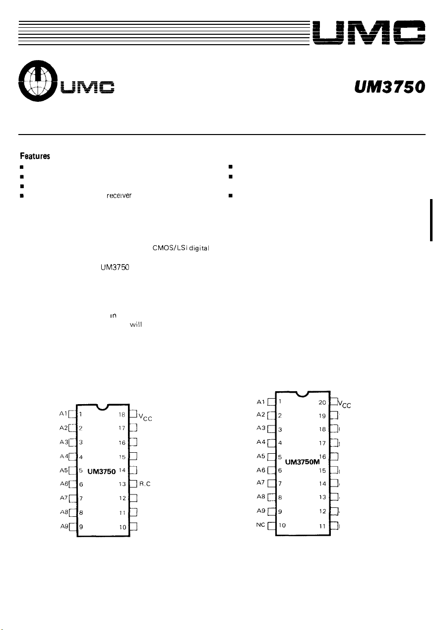
Pin Configurations
TX/RX OUTPUT
RECEIVER INPUT
MODE SELECT
“ss
A12
All
A10
Schmitt Trigger input provides excellent noise immunity.
Applications. alarm control system, security system
cordless telephone, remote control.
Interfaces with RF, ultrasonic, or infrared modulators
and demodulators
comparison on the next word.
correctly, a “valid” signal is generated. This signal
64ms counter and triggers a
If all 12 bits are
3-stage
counter. The
received
clears a
3-stage
counter counts the “valid” pluses and when 4 pulses have
been detected, the TX/RX output pin goes low. After the
TX/RX output pin goes low, the next “valid” must be
received within
128ms,
giving a one valid in 6 requirement
to keep the TX/RX output pin.
TX/RX OUTPUT
RECEIVER INPUT
MODE SELECT
“SS
R.C.
INPUT
A12
All
A10
NC
I
2-3
Page 2
Block
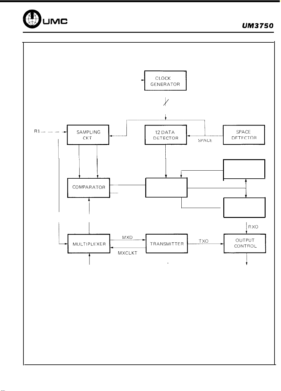
Diagram
R.C.INPUT - - - - - -
CPCLK
RID
COMPARATOR
MXCLKR
MXD
-
ERROR
CLR
WD
STATE
CONTROLLER
TIM0
VLD
INIT
64ms/128ms
TIMER
VALID 4
COUNTER
Al-Al2
Block
Diagram Description
CPCLK
WXCLKR: CLK of Multiplexer when in Receiver mode
WXCLKT
MXD:
RID
VLD.
CLK of Comparator
CLK of Multiplexer when in Transmitter mode
Output data of Multiplexer (one of Al, A2
A12)
Sampled data by Sampling CKT
“Valid” signal. It is used to trigger Valid 4
Counter and
reset 64ms/128ms
Timer
....
2-4
CLR:
ERROR:
TIMO :
T/R OUT:
INIT:
WD:
TXO:
PXO:
Clear signal of Comparator
Error signal from Comparator
TIMER time-out signal
Transmit/Receiver output pin
Reset signal of Valid 4 Counter
Word detected signal
Transmitter output
Receiver output
T/R
OUT
(64ms or 128ms)
Page 3

Absolute Maximum Ratings*
Power Supply Voltage
Operating Temperature -20 Deg to
Storage Temperature
Applied Voltage on any Pin
--55 Deg to 150 Deg C
<
3v to 11v
Deg C
+o 3
*Comments
Stresses above those
Ratings” may cause permanent damage to the
These are stress ratings only.
this device at these or any other conditions above those
in the operational sections of this
not
conditions for extended
and exposure to absolute
Iunder “Absolute Maximum
Functional operation of
rating
may affect device
D.C. Electrical Characteristics
Input Level
Input Resistor
to Vcc
Frequency
Pin Designation
Pin No.
l-12
13
Designation
Al
Al2
R.C. INPUT
=
=
otherwise specified)
_
F
200K
_
_
100
_
KHz
exclusive
of external
components
Description
These data select
They have
R.C. input
to
and a
are used to set the addresses of the encoder/decoder
pull-up resistors.
for
oscillator. A
from
to GND
hooked from
The frequency =
14
15
16
17
18
MODE SELECT
RECEIVER
INPUT
OUTPUT
Vcc
The ground
grounding
to
The receiver input receives the digital PCM waveform
The
of the UM3750.
the IC from Receive mode
pin
IC
the IC
mode,
In the receive mode,
result and detects low
power supply
put Into the Receive mode. By connecting
output
Transmit mode, By
mode
produces the PCM waveform for
comparison is ok.
output
of the UM3750.
provides the
2-5
the detect
Page 4

_
Connection Diagram for Transmitter/Receiver
Output Waveform (based on 100 KHz)
Typical
2-6
Page 5

Decoder Flowchart
No
Stand by Mode
Reset Count
Yes
No
Data
Ordering Information
Count
eset 64m s,
Activates the
Count +1
Timer
Output
Output
Part No. Package
NO
is
64ms Timer
Overflow
No
Yes
Yes
2-7
 Loading...