

Page 1

QorIQ T1040 Reference Design Board
User Guide
Document Number: T1040RDBPAUG
Rev. 0, 06/2015
Page 2

QorIQ T1040 Reference Design Board User Guide, Rev. 0, 06/2015
2 Freescale Semiconductor, Inc.
Page 3

Contents
Section number Title Page
Chapter 1
Overview
1.1 Related documentation....................................................................................................................................................7
1.2 Acronyms and abbreviations...........................................................................................................................................7
1.3 Silicon features................................................................................................................................................................8
1.4 Board features................................................................................................................................................................. 9
1.5 Block diagram.................................................................................................................................................................10
Chapter 2
Architecture
2.1 Processor.........................................................................................................................................................................13
2.2 Power.............................................................................................................................................................................. 13
2.3 Clocks............................................................................................................................................................................. 15
2.4 Reset................................................................................................................................................................................18
2.5 DDR................................................................................................................................................................................18
2.6 SerDes port......................................................................................................................................................................20
2.6.1 PCIe support.......................................................................................................................................................21
2.6.2 SGMII support................................................................................................................................................... 22
2.6.3 QSGMII support................................................................................................................................................ 22
2.6.4 SATA support.................................................................................................................................................... 23
2.7 Ethernet controllers.........................................................................................................................................................23
2.8 Ethernet management interface.......................................................................................................................................24
2.9 I2C...................................................................................................................................................................................25
2.10 SPI interface....................................................................................................................................................................26
2.11 Local bus.........................................................................................................................................................................27
2.12 SDHC interface...............................................................................................................................................................28
2.13 USB interface..................................................................................................................................................................29
2.14 Serial port........................................................................................................................................................................30
2.15 SLIC/SLAC and TDM interface.....................................................................................................................................32
QorIQ T1040 Reference Design Board User Guide, Rev. 0, 06/2015
Freescale Semiconductor, Inc. 3
Page 4

Section number Title Page
2.16 JTAG/COP port.............................................................................................................................................................. 33
2.17 Connectors, headers, jumper, push buttons and LED.....................................................................................................34
2.17.1 Connectors......................................................................................................................................................... 35
2.17.2 Headers...............................................................................................................................................................36
2.17.3 Jumper................................................................................................................................................................ 36
2.17.4 Push buttons....................................................................................................................................................... 37
2.17.5 LEDs.................................................................................................................................................................. 37
2.18 Temperature.................................................................................................................................................................... 37
2.19 DIP switch definition......................................................................................................................................................38
Chapter 3
CPLD specification
3.1 CPLD programming........................................................................................................................................................41
3.2 CPLD memory map........................................................................................................................................................44
3.2.1 Chip ID1 register (CHIPID1).............................................................................................................................44
3.2.2 Chip ID2 register (CHIPID2).............................................................................................................................45
3.2.3 Hardware version register (HWVER)................................................................................................................45
3.2.4 Software version register (SWVER)..................................................................................................................46
3.2.5 Reset control register (RSTCON1).................................................................................................................... 46
3.2.6 Reset control register (RSTCON2).................................................................................................................... 47
3.2.7 INTSR................................................................................................................................................................ 48
3.2.8 Flash control and status register (FLHCSR)...................................................................................................... 49
3.2.9 Fan control and status register (FANCSR)........................................................................................................ 49
3.2.10 Panel LED control and status register (LEDCSR).............................................................................................50
3.2.11 SFP+ control and status register (SFPCSR).......................................................................................................51
3.2.12 Miscellaneous control and status register (MISCCSR)..................................................................................... 51
3.2.13 Boot configuration override register (BOOTOR).............................................................................................. 52
3.2.14 Boot configuration register 1 (BOOTCFG1)..................................................................................................... 52
3.2.15 Boot configuration register 2 (BOOTCFG2)..................................................................................................... 52
QorIQ T1040 Reference Design Board User Guide, Rev. 0, 06/2015
4 Freescale Semiconductor, Inc.
Page 5

Section number Title Page
Chapter 4
Software configuration
4.1 Preparing board...............................................................................................................................................................55
4.2 Ethernet port map............................................................................................................................................................57
4.3 NOR flash image layout..................................................................................................................................................57
4.4 Switch settings................................................................................................................................................................ 58
4.4.1 Switch default settings (NOR flash boot).......................................................................................................... 58
4.4.2 Other boot source settings..................................................................................................................................59
4.4.3 Switch detailed description................................................................................................................................ 59
4.5 SDK Build details........................................................................................................................................................... 60
4.6 Flashing and updating images.........................................................................................................................................60
4.6.1 Flashing images on and booting from NOR flash..............................................................................................60
4.6.2 Flashing eSPI boot images................................................................................................................................. 61
4.6.3 Flashing NAND boot images............................................................................................................................. 62
4.6.4 Flashing SD card boot images........................................................................................................................... 63
4.6.5 Booting Linux.................................................................................................................................................... 63
QorIQ T1040 Reference Design Board User Guide, Rev. 0, 06/2015
Freescale Semiconductor, Inc. 5
Page 6

QorIQ T1040 Reference Design Board User Guide, Rev. 0, 06/2015
6 Freescale Semiconductor, Inc.
Page 7

Chapter 1
Overview
This manual describes the features and operation of a high performance reference
platform that supports QorIQ Power Architecture® processors including:
• T1040
• T1020
The T1040RDB is optimized to support high-bandwidth DDR3L memory and a full
complement of high-speed SerDes ports.
NOTE
The dual-core version of the T1040 SoC is known as T1020.
1.1 Related documentation
The documents below may be available only under a non-disclosure agreement (NDA).
To request access to these documents, contact your local field applications engineer or
sales representative.
Table 1-1. Related documentation
Document name Description
QorIQ T1040, T1020 Data Sheet
(T1040, T1020)
QorIQ T1040 Reference Manual
(T1040RM)
QorIQ T1040 Reference Design Board User Guide, Rev. 0, 06/2015
Freescale Semiconductor, Inc. 7
Provides specific data regarding bus timing, signal behavior, and AC, DC, and thermal
characteristics, as well as other design considerations
This document provides a detailed description on the QorIQ T1040 multicore processor,
and its features, such as memory map, serial interfaces, power supply, chip features,
and clock information.
Page 8

Silicon features
1.2 Acronyms and abbreviations
The following table contains acronyms and abbreviations used in this document.
Table 1-2. Acronyms and abbreviations
Term Description
COP Common On-chip Processor
CPC CoreNet Platform Cache
CPLD Complex Programmable Logic Device
DIMM Dual in-line memory module
DIP Dual in-line package
DMA Direct Memory Access
DPAA Data Path Acceleration Architecture
DRAM Dynamic random-access memory
DUT Device under test
ECC Error detection and correction
EMI Ethernet Management interface
eSDHC Enhanced Secure Digital Host Controller
eSPI Enhanced Serial Peripheral Interface
FXS Foreign Exchange Station
FXO Foreign Exchange Office
I2C Inter - Integrated Circuit
IFC Integrated Flash Controller
JTAG Joint Test Action Group
MDC Management Data Clock
MDIO Management Data Input/Output
PCIe PCI Express
POR Power-on reset
PSU Power Supply Unit
QMan Queue Manager
SATA Serial Advanced Technology Attachment
SD Secure Digital
SerDes Serializer/Deserializer
SGMII Serial Gigabit Media Independent Interface
SPI Serial Peripheral Interface
SYSCLK System Clock
UART Universal asynchronous receiver/transmitter
VCC Voltage for circuit
VTT Voltage for terminal
QorIQ T1040 Reference Design Board User Guide, Rev. 0, 06/2015
8 Freescale Semiconductor, Inc.
Page 9

1.3 Silicon features
NOTE
For a description of the features of the T1040 SoC, see QorIQ
T1040 Reference Manual (T1040RM).
1.4 Board features
The features of the T1040RDB-PA board are as follows:
Eight lanes of SerDes connections with support for:
•
• PCIe that supports Gen 1 and Gen 2
• SGMII
• QSGMII
• SATA 2.0
• DDR controller
• Supports data rates up to 1600 MHz
• Supports one DDR3L DIMM of single-, dual-, or quad-rank type
• DDR power supply (1.35 V) with automatic tracking of VTT
• IFC
• NAND flash: 8-bit, async, 1 GB
• NOR: 16-bit, non-multiplexed, 128 MB, support of eight virtual banks
• Ethernet
• Two onboard RGMII 10/100/1G Ethernet ports, PHY #0 remains powered up
during deep-sleep
• One onboard SGMII 10/100/1G Ethernet Port
• Two onboard QSGMII 10/100/1G PHYs connecting to 8 GE ports
• CPLD
• Manages system power and reset sequencing
• Manages DUT, board, clock configuration
• Reset and interrupt monitor and control
• General fault monitoring and logging
• Sleep mode control
• Clocks
• SYSCLK at 100 MHz
• DDRCLK at 66.66 MHz
• USBCLK at 24 MHz
• Single Oscillator Source reference clocking at 100 MHz
• Power Supplies
Chapter 1 Overview
QorIQ T1040 Reference Design Board User Guide, Rev. 0, 06/2015
Freescale Semiconductor, Inc. 9
Page 10

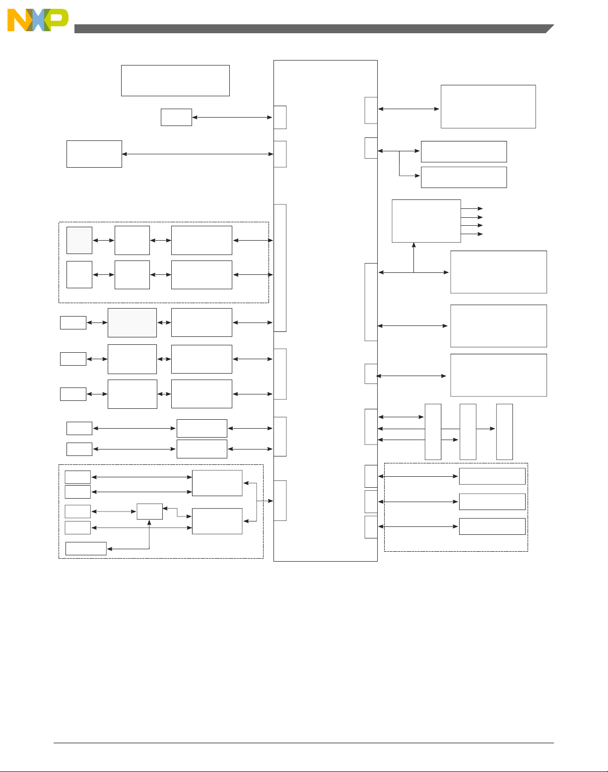
(Peripheral access
management unit)
C
oreNet™ Coherency Manager
Security monitor
Power management
SD/eSDHC/eMMC
2x DUART
16b IFC
eSPI, 4x GPIO
32/64-bit
DDR3L/4
memory controller
Real-time
debug
Watchpoint
cross
trigger
Perf
Monitor
2 x USB2.0 w/PHY
4x I2C
Power Architecture
®
e5500
32 KB
D-Cache
32 KB
I-Cache
256 KB
backside
L2 cache
256 KB
platf
orm cache
Security fuse processor
DIU
Security
5.4
(XoR,
CRC)
P
attern
match
engine
2.2
Queue
Manager
Buf
fer
Manager
1G 1G 1G
Parse, classify,
distr
ibute
8-port
s
witch
1G 1G 1G 1G
1G 1G 1G 1G
2x DMA
PCl Express 2.0
PCI Express 2.0
PCI Express 2.0
PCI Express 2.0
SATA 2.0
SATA 2.0
TDM/HDLC
TDM/HDLC
QUICC
Engine
Trace
8-lane, 5 GHz SerDes
PAMU
Frame Manager
1G
Aurora
Block diagram
• Dedicated PMBus regulator for core power adjustable from 0.7 V to 1.3 V at 35
A
• USB
• Supports two USB 2.0 ports with integrated PHYs. Two type A ports with 5
V@1.5 A per port
• SDHC port that connects directly to card slot
• SPI
• One onboard 64 MB SPI flash
• Onboard support of SPI EEPROM, TDM SLAC control, and TDM riser card
control
• TDM interface through optional riser card, also support FXS/FXO on board
• I2C bus
• Devices connected: EEPROM, thermal monitor, VCore power controller
• Other IO
• Two serial ports
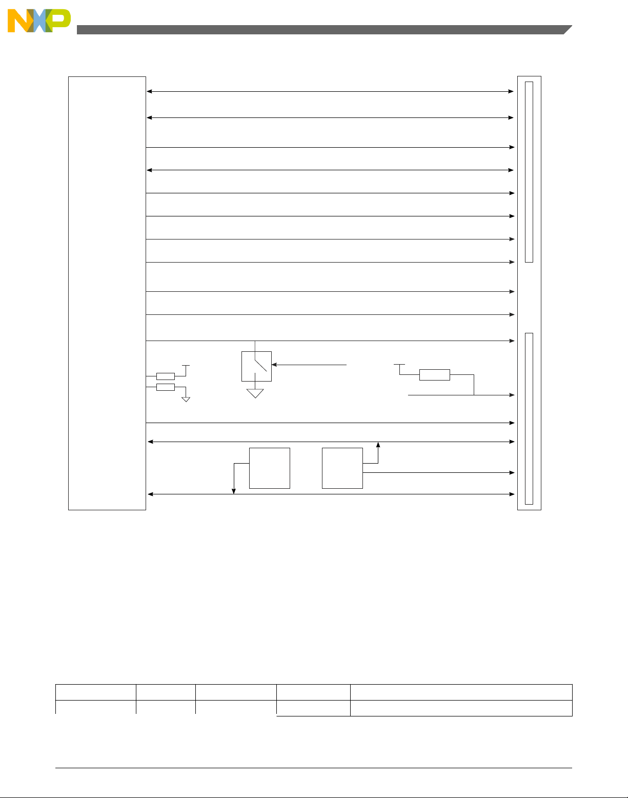
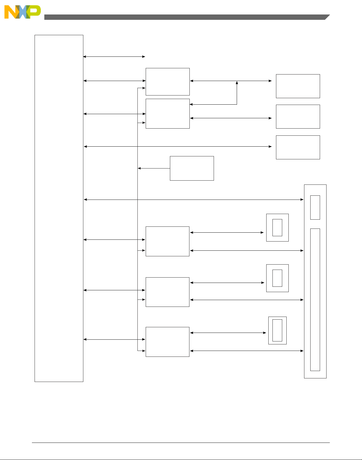
1.5 Block diagram
This section provides a high-level overview of the T1040 SoC and the T1040RDB board.
The figures below show the major functional units within the T1040 device and the
T1040RDB board.
10 Freescale Semiconductor, Inc.
QorIQ T1040 Reference Design Board User Guide, Rev. 0, 06/2015
Figure 1-1. T1040 SoC block diagram
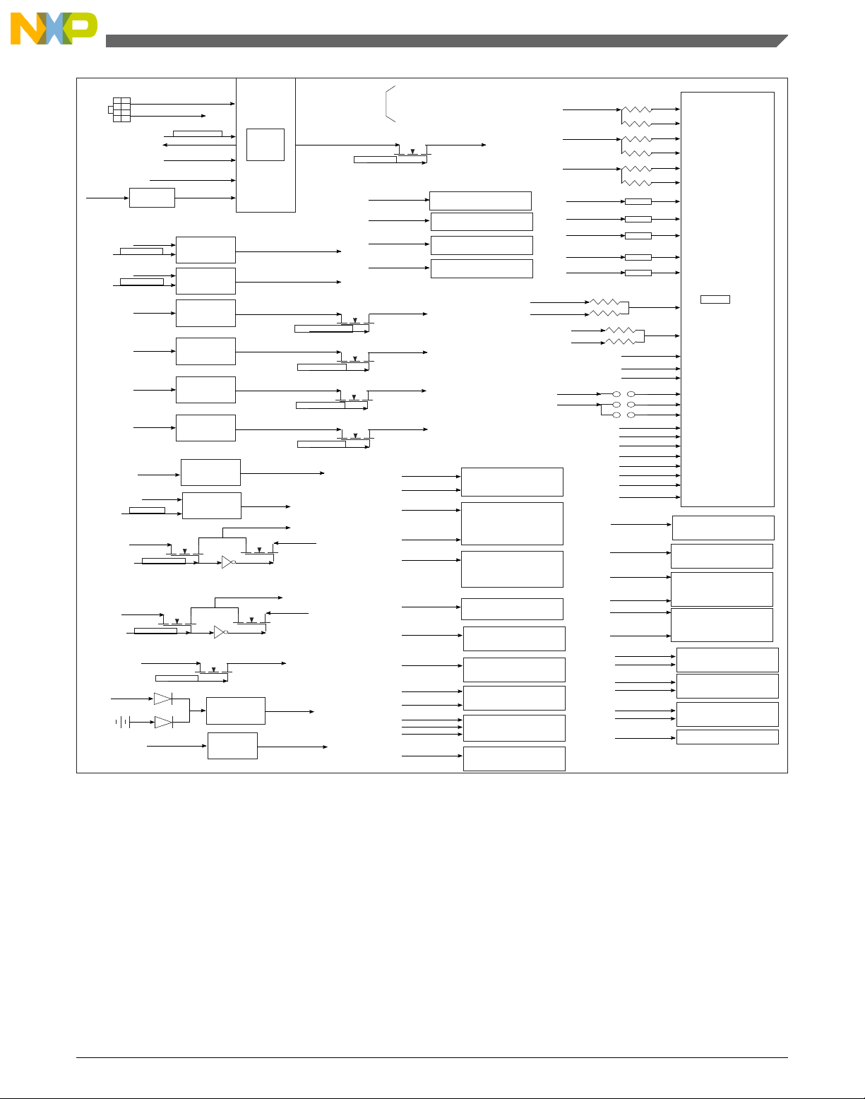
Page 11
Clocks, POR, reset and
po
wer supply circuit
JTAG
USB Type A x2
USB Conn *2
DDR3L 72bit
I2C_1
MT18KSF71272HZ-1G6 (4GB)
1.6G,DDR3L/72bit 4GB
(UDIMM)
Address:0x4c
Address:0x50
EEPROM(AT24C256)
Temp sensor (ADT7461)
CPLD
(EPM240G)
RESET
Interrupt
Power on conf
Other control
Local bus (16bit)
Local bus (8bit)
SPI bus
NOR FLASH
S29GL01GP11TFIV10
(128MB)
PCIe x1
SATA (T1040 only)
SDXC Card
T1/E1
QUICC Engine connector for
PMC plug-in card
QUICC Engine
Interface
SATA
RJ45
TXD,RXD,RTS,CTS
RGMII
SGMII
T1040
IFC
SPISATA
QE
TDM
DUART
RGMII
USB2.0
COP
DDR3
I2C
Mini PCle
PClex1
QSGMII
QSGMII
F104S8A
(QGMII->Copper)
Magnetic
X4
Magnetic
X4
RJ45
X4
RJ45
X4
Magnetic
(GSTS009LF)
RTL8211DN
(SGMII>Copper)
2Pin-Conn
FX
O
Relay
FXS1
Le88266DLC
MAX3232
SerDes
RJ45
RJ45
RJ45
RJ45
RJ1
1
RJ11
RJ11
RJ11
FXS2
FXS3
FXS4
TXD,RXD,RTS,CTS
Le88266DLC
MAX3232
RGMII
F104S8A
(QGMII->Copper)
Magnetic
(GSTS009LF)
Magnetic
(GSTS009LF)
RTL8211E-VB
(RGMII->Copper)
RTL8211E-VB
(RGMII->Copper)
SDXC PCle
NAND FLASH
MT29F8G08ABABAWP.121T
(1GB)
SPI FLASH
N25Q512A13GSF40F
(64MB)
Mini PCle
PCIe x1
PCIe x1
Chapter 1 Overview
Figure 1-2. T1040RDB board block diagram
Freescale Semiconductor, Inc. 11
QorIQ T1040 Reference Design Board User Guide, Rev. 0, 06/2015
Page 12

Block diagram
QorIQ T1040 Reference Design Board User Guide, Rev. 0, 06/2015
12 Freescale Semiconductor, Inc.
Page 13

Chapter 2
Architecture
This section explains:
• Processor
• Power
• Clocks
• Reset
• DDR
• SerDes port
• Ethernet controllers
• Ethernet management interface
• I2C
• SPI interface
• Local bus
• SDHC interface
• USB interface
• Serial port
• SLIC/SLAC and TDM interface
• JTAG/COP port
• Connectors, headers, jumper, push buttons and LED
• Temperature
• DIP switch definition
2.1 Processor
The T1040RDB supports as many features of the T1040 as possible, as detailed in the
following sections. The T1040RDB supports this by isolating OVDD-powered signals
through external translation devices or the CPLD wherever required.
QorIQ T1040 Reference Design Board User Guide, Rev. 0, 06/2015
Freescale Semiconductor, Inc. 13
Page 14

Power
2.2 Power
The power supply system of the T1040RDB board uses power from a standard ATX
power supply unit (PSU) to provide the required power supplies to the processor, CPLD,
and peripheral devices. In addition to meeting required power specifications, the
following goals guide the power supply architecture:
• Monolithic power supply for VCC that powers internal cores and platform logic
• T1040RDB can access IR36021 via software to check the current and voltage values
or to program the voltage changes
• All power supplies are sequenced per hardware specifications
The figure below shows an overview of the power supply.
QorIQ T1040 Reference Design Board User Guide, Rev. 0, 06/2015
14 Freescale Semiconductor, Inc.
Page 15
BEAD
ATX PS
12V_SLP
5V0_SLP
VCORE_EN
VCORE_PGOOD
CPLD
PM_BUS
VPG
R
egulator
IR36021/
3550
3V3_SLP
VCC_DRV_3.3V
VCC_DRV_7V
12V_SLP
MIC30102
YM
SVO_SLP
IOPWR_EN
1V0 (4A)
1V5 (1.5A)
IR3473
1V35
1V8
2V5
3V3
VTT/MVREF
1V0S
DVDD
MIC47100
TPS51200
1V35_SLP
1V8_SLP
VDD_EN
2V5
EVDD_SEL
For T1040,DVDD=3.3V
3V3
EVDD
3V3
1V8
T2081_EN
12V_SLP
OPWR_EN
3V3
12V
1V0_LP
NCP571
12V
BATH/BATL
DC/DC
3V3
OVDD_SLP
3V3_SLP
1V8_SLP
EPM570
VDD
PCA9546
BATH/BATL
3V3
5V0_SLP
USB:MIC2506
DVDD/AVDD
Le88266*2
SD Card
IN
VDD
3V3
SPI FLASH
N25QS1
2A13G
VCC
3V3
3V3
NAND FLASH
MT29F8G08ABB
AWP
VCC/VCOD
VIO
OVDD
3V3
VCC
NOR FLASH
JS28F00AM29EWHA
2V5
VDD25/VDD25A
VSC8514*2
VDD1/VDD1A
1V0
OVDD_SLP
VCCRE
J11
IDT9FGV0641
ICS843002*2
3V3
1V8_SLP
OVDD
OVDD_SLP
100M OSC
S
ys_refclk
66.67M OSC
DDR_r
efclk
VCORE_SLP_40A
VCORE
VDD_EN
VCORE_EN
CPLD
1V35
OVDD_SLP
0.33ohm
OVDD
VCORE_SLP
3V3_SLP
OVDD_SLP
1V05
1V35
1V8_SLP
3V3_SLP
1V8
3V3
0ohm[NC]
MVREF
1V0_LP
OVDD
OVDD
OVDD_SLP
0ohm[NC]
0ohm
BEAD
XVDD
AVDD_SD1_PLL1
AVDD_SD1_PLL2
AVDD_PLAT
AVDD_D1
AVDD_CGA1
AVDD_CGA2
USB_SVDD[1:2]
USB_HVDD[1:2]
USB_OVDD[1:2]
S1VDD[1:7]
X1VDD[1:5]
T1040
O1VDD[1:3]
OVDD[1:8]
D1_MVREF
VDD_IP
TH_VDD
FA_VL
PROG_MTR
PROG_SFP
EVDD1
DVDD[1:3]
CVDD1
LVDD[1:2]
L1VDD[1:2]
G1VDD[1:19]
VDD[1:47]
VDDC[1:7]
PIPCIE3212*5
VDD
3V3
3V3
3V3_SLP
VDD
MAX3232*2
AVDD/DVDO
RTL8211E-VB
U49
DVDD(15/21)
2V5_SLP
3V3
AVDD/DVDD
RTL8211E-VB/DN
U46/U52
DVDD(15/21)
2V5
3V3
12V
3V3
12V
TDM SLOT
PCIEX4 SLOT
1V5
3V3
MINI PCIE SLOT*2
12V
FAN Conn *4
SVO_SLP
IOPWR_EN
IR3473
IR3473
SVO_SLP
IR3473
SVO_SLP
IR3473
SVO_SLP
IR3473
SVO_SLP
OPWR_EN
(Always_On)
3V3_SLP(9A)
OPWR_EN
(Always_On)
2V5_SLP(1.5A)
ODRPWR_EN
(Always_On)
1V35_SLP(6.5A)
(Switchable)
(Switchable)
VDD_EN
IOPWR_EN
DDRPWR_EN
EVDD_SEL
T2081_EN
OPWR_EN
(Always_On)
1V8_SLP(2A)
SVDD
0ohm
BEAD
BEAD
BEAD
0.33ohm
5.1ohm
5.1ohm
5.1ohm
5.1ohm
J10
J9
EVDD
DVDD
OVDD
2V5
2V5_SLP
1V5_SLP
VCORE
VCORE_SLP
Chapter 2 Architecture
2.3 Clocks
The clock circuitry provides clocks for the processor for:
•
SYSCLK (single-ended and differential)
• DDRCLK
• SerDes clocks (two independent options)
QorIQ T1040 Reference Design Board User Guide, Rev. 0, 06/2015
Freescale Semiconductor, Inc. 15
Figure 2-1. Power distribution
Page 16

Clocks
• Ethernet clocks
• USB clock
The architecture of the clock section is shown in the figure below.
QorIQ T1040 Reference Design Board User Guide, Rev. 0, 06/2015
16 Freescale Semiconductor, Inc.
Page 17
P
E
X
S
L
O
T
M
I
N
I
P
E
X
S
L
O
T
M
I
N
I
P
E
X
S
L
O
T
25MHz
ICS843002
(ONL
Y FOR T1040)
125MHz
ICS843002
25MHz
OSC-100MHz
OSC-66.66MHz
OSC-24MHz
IDT9FGV0641
DIFSYSCLK_OE
PEXCLK_OE
25MHz
MPEX2_REFCLK_P/N(100M)
T1040
DDRCLK (66.66MHz)
USB_REFCLK (24MHz)
SYSCLK (100MHz)
SD_REFCLK1_P/N
(125MHz)
QSG2_REFCLK_P/N
(125MHz)
QSG1_REFCLK_P/N
(125MHz)
F104S8A
F104S8A
MPEX1_REFCLK_P/N(100M)
PEX_REFCLK_P/N(100M)
SD_REFCLK2_P/N(100M)
SYS_REFCLK_P/N(100M)
Chapter 2 Architecture
Figure 2-2. Clock distribution
QorIQ T1040 Reference Design Board User Guide, Rev. 0, 06/2015
Freescale Semiconductor, Inc. 17
Page 18
ATX PS
PWR_GODD
GND
Push-Button
MAX811S
(Power-on RST)
PON_RST_N
COP_SRST_N
COP_ITF
T1040
HESET_REQ_N
HRSET_N
PORESET_N
Reset
source
select
RST_CTL
DDR_RSTN
TDMR_RST
TDMR
SLOT
QSG2_RST_N
QSGMII
GE PHY
QSG1_RST_N
EC1_RST_N
RGMII
GE PHY1
Soft reset register
RSTCON1 & RSTCON2
SW_RST
7
CPLD
COP_HRST_N
6
5
4
3
2
1
0
EC2_RST_N
RGMII
GE PHY2
DDR3/
DDR3L
CORE_power
(IR36021)
VCORE_PGD
NOR
FLASH
PEX SLOT
MINI PEX
SLOT
MINI PEX
SLOT
SGMII
GE PHY
QSGMII
GE PHY
MPEX2_RST
PEX_RST
MPEX1_RST
NOR_RSTN
SG_RST_N
Reset
2.4 Reset
The CPLD manages the reset signals to and from the T1040 processor and the other
devices on the T1040RDB board. The figure below shows an overview of the reset
architecture.
Figure 2-3. CPLD logical
2.5 DDR
The T1040RDB supports high-speed DRAM with an unbuffered DDR3L (240pin) socket
(UDIMM), featuring single-, dual-, and quad-rank support. The memory interface
includes all the necessary termination and I/O power, and is routed so as to achieve
maximum performance of the memory bus, as shown in the below figure.
QorIQ T1040 Reference Design Board User Guide, Rev. 0, 06/2015
18 Freescale Semiconductor, Inc.
Page 19
IV35_SLP
DDR_DQ[0:63]
DDR_ECC[0:7]
DDR_MA[0:1
5]
DDR_MDQS[0:8]
DDR_MDM[0:8]
DDR_MBA[0:2]
DDR_MDOT[0:1],DDR_MAPAR_OUT,DDR_MPAR_ERR
DDR_MCS[0:3]
DDR_MCK_P[0:1]_P/N
DDR_CAS,DDR_RAS,DDR_WE
DDR_MCKE[0:1]
IV35_SLP
DDR_RST_N
(CPLD)
I2C1_SCL,I2C1_SDA
MV_REF
VTT
IV35_SLP
(SPD_ADDR-0X51)
DDR3 DIMM SOCKET 240PIN
DIMM
T1040
DL_MDIC1
DL_MDIC0
IR3475
TPS
51200
For T1040:R-162Ohm
CKE_ISO_EN(CPLD)
Chapter 2 Architecture
Figure 2-4. T1040 and DDR connection
Although the platforms support all types, ranks and speeds of DIMMs within the
specification of the T1040, not all combinations of these three exist on the memory
market. Thus, the system is shipped with a “representative” DIMM, as noted in the below
table.
Other suitable memory DIMMs can be purchased and installed if needed; however,
Freescale only supplies the device shown.
Platform Type Speeds Ranks DIMM
Table 2-1. DDR3L UDIMM support
T1040RDB DDR3L 1600 MT/s Single Micron MT9KSF51272AZ-1G6
Table continues on the next page...
QorIQ T1040 Reference Design Board User Guide, Rev. 0, 06/2015
Freescale Semiconductor, Inc. 19
Page 20

SerDes port
Table 2-1. DDR3L UDIMM support (continued)
Dual Micron MT18KSF51272AZ-1G6
Quad (TBD)
2.6 SerDes port
The T1040 SerDes block provides eight high-speed serial communication lanes
supporting a variety of protocols, including:
SGMII 1.25 Gbit/s
•
• QSGMII 5 Gbit/s
• PCIe Gen 1 x1 2.5 Gbit/s
• PCIe Gen 2 x1 5 Gbit/s
• SATA x1 1.5/3 Gbit/s
The following table explains the SerDes protocols supported on the T1040RDB board.
Table 2-2. SerDes protocol distribution
SerDes
SRDS_PRTCL A B C D E F G H Option
T1040/T1020 PCIe SGMII QSGMII QSGMII PCIe PCIe PCIe SATA 0x66
To comply with T1040 specifications, multiplexers are used to re-route and group the
SerDes lanes as shown in the figure below.
QorIQ T1040 Reference Design Board User Guide, Rev. 0, 06/2015
20 Freescale Semiconductor, Inc.
Page 21
T1040
SD1_RXn/TXn_P/N
PI3PCIE321
2
SGMII_RX/TX
RTL8211DN
(SGMII_PHY)
F104S8A
(QSGMII_PHY)
SD1_RXn/TXn_P/N(QSGMII2_RX/TX)
CPLD
SD1_RXn/TXn_P/N(PEX[0])
MPEX[1]
PEX[1]
Mini_PCle
SLOT
SATA
SD1_RXn/TXn_P/N
SD1_RXn/TXn_P/N
SD1_RXn/TXn_P/N
SD1_RXn/TXn_P/N
PI3PCIE3212
PI3PCIE3212
PI3PCIE3212
PI3PCIE3212
QSGMII1_RX/TX
MPEX[2]
PEX[2]
PEX[3]
SATA
Mini_PCle
SLOT
PCle SLOT
F104S8A
(QSGMII_PHY)
n - [0:7]
SD1_RXn/TXn_P/N
Chapter 2 Architecture
Figure 2-5. SerDes lane connections
QorIQ T1040 Reference Design Board User Guide, Rev. 0, 06/2015
Freescale Semiconductor, Inc. 21
Page 22

T1040
SGMII
MDIO/MDC
R
TL8211DN
Transformer
RJ-45 Port
EMI1
SGMII
SerDes port
2.6.1 PCIe support
The T1040RDB supports evaluation of PCIe using any standard PCIe Gen 1/Gen 2 card.
2.6.2 SGMII support
The T1040RDB board supports evaluation of the SGMII protocol using the RTL8211DN
PHY.
The figure below shows the connectivity of the SGMII interface.
Figure 2-6. SGMII connection
2.6.3 QSGMII support
The T1040RDB board supports evaluation of the QSGMII protocol using an F104S8A
four-port Ethernet PHY. The figure below shows the connectivity of the QSGMII
interface.
22 Freescale Semiconductor, Inc.
QorIQ T1040 Reference Design Board User Guide, Rev. 0, 06/2015
Page 23

QSGMII
T1
040
EMII
QGMII
QSGMII
F104S8A
Transformer
Transformer
RJ-45 Port
RJ-45 Port
QGMII
F104S8A
MDIO/MDC
2.6.4 SATA support
Chapter 2 Architecture
Figure 2-7. QSGMII connection
SATA may be evaluated through an onboard SATA connector.
2.7 Ethernet controllers
The T1040 SoC supports two Ethernet controllers (EC), which can connect to the
Ethernet PHYs using the MII or RGMII protocols. On the T1040RDB board, the EC1
and EC2 ports operate in the RGMII mode only. Both ports connect to the Realtek
RTL8211 PHYs. The T1040RDB board supports energy efficient Ethernet on EC1 and
sleep mode on EC2.
The figure below shows the connectivity of the EC1 and EC2 interfaces.
Freescale Semiconductor, Inc. 23
QorIQ T1040 Reference Design Board User Guide, Rev. 0, 06/2015
Page 24

RGMII
ETH. Cntr. 1
T1040
EMI1
RGMII
RGMII
RTL8211E_VB
Transformer
Transformer
RJ-45 Port
RJ-45 Port
ETH. Cntr. 2
RGMII
RTL8211E_VB
MDIO/MDC
Ethernet management interface
Figure 2-8. RGMII connection
2.8 Ethernet management interface
The T1040 Ethernet management interface (EMI1) is used with the onboard RGMII,
SGMII, and QSGMII PHYs. The figure below shows the EMI block.
QorIQ T1040 Reference Design Board User Guide, Rev. 0, 06/2015
24 Freescale Semiconductor, Inc.
Page 25

OE
2V5
2V5_SLP
EMII_MDC_SLP
EMII_MDIO_SLP
R
TL8211E-VB
(RGMII PHY)
PHY_ADDR=0X01
RTL8211E-VB
(RGMII PHY)
RTL8211DN
(SGMII PHY)
F104S8A
(QSGMII PHY)
F104S8A
(QSGMII PHY)
PHY_ADDR-0X02
PHY_ADDR-0X03
PHY_ADDR-0X04-07
PHY_ADDR-0X08-08
T1040
74LVC1G66*2
Chapter 2 Architecture
Figure 2-9. Management Data Input/Output (MDIO) connection
2.9 I2C
The T1040 devices support up to four I2C buses in order to make the I2C resources
equally available to both local and remote systems. The T1040RDB board uses I2C1 port
to access onboard devices, such as SPD on the DDR3L DIMM, thermal sensor
(ADT7461), and core power regulator (IR36021) . The I2C2 bus uses multiplexers to
partition the I2C bus into several sub-buses, called channels. The two mini-PCIe slots use
channel 0-1, or I2C2_CH0-1, channel 2 is unused on the T1040RDB board. The PCIe
slot uses channel 3.
The figure below shows the I2C subsystem.
QorIQ T1040 Reference Design Board User Guide, Rev. 0, 06/2015
Freescale Semiconductor, Inc. 25
Page 26

FET Isolation
(IRLML6346)
I2C1
I2C1_SCL
DDR3 DIMM
ADT7
461
(Thermal sensor)
AT24C256
I2C_ADDR=0x51
Mini_PCle SLOT
Mini_PCle SLOT
PCle SLOT
I2C2_SDA
I2C2_SCL
I2C2
PCA9546
Channel 0
I2C_ADDR-0X77
T1040
I2C1_SDA
I2C2_MPEX2_SCL
I2C2_MPEX2_SDA
I2C2_PEX_SCL
I2C2_PEX_SDA
I2C_ADDR=0x4C
I2C_ADDR=0x50
I2C_ADDR=0x08
Test_mode_ADDR=0x0A
I2C_ADDR=0x6A
DVDD
I2C2_MPEX1_SCL
I2C2_MPEX1_SD
A
FET
Isolation
3V3
I2C1_SCL_SLP
IR36021
(C
ore_Power)
IDT9FGV0641
I2C1_SDA_SLP
Channel 1
Channel 2
Channel 3
SPI interface
Figure 2-10. I2C bus connection
2.10 SPI interface
The T1040 serial peripheral interface (SPI) pins are used for the following purposes:
• Onboard SPI device access to various SPI memory devices
QorIQ T1040 Reference Design Board User Guide, Rev. 0, 06/2015
26 Freescale Semiconductor, Inc.
Page 27

SPI
T1040
PROC_SPI_CS0-3
PROC_SPI_MOSI/MISO_CLK
OVDD-1.8V
3.3V
SPI_MOSI/MISO_CLK
TXBN0304
(OVDD to 3.3V)
SPI_CS3
SPI_CS2
SPI_CS1
Le88266
(SLAC)
Le88266
(SLAC)
TDM Riser card connector
N25Q512A
(64MB FLASH)
SPI_CS0
Chapter 2 Architecture
• Offboard (TDM riser) device
• Onboard SLAC device access
SPI 0 is connected to the SPI EEPROM. SPI 1 and 2 are connected to the SLAC chips for
FXS voice support and SPI 3 is connected to the TDM riser card connector.
The figure below shows the overall connections of SPI.
Figure 2-11. SPI bus connections
2.11 Local bus
The T1040 Integrated Flash Controller (IFC), also called the local bus, supports 32-bit
addressing and 8- or 16-bit data widths, for a variety of devices. IFC lets to manage all
these resources effectively with maximum performance and flexibility. The figure below
shows an overview of the IFC bus.
QorIQ T1040 Reference Design Board User Guide, Rev. 0, 06/2015
Freescale Semiconductor, Inc. 27
Page 28

T1040
ADDR[0,31], DATA[0,15], Control
TXBN0304
(1
.8V->3.3V)
CPLD
Cfg_vbank[0:2]
IFC_A5-A7
XORs
IFC_VA5-7
NOR_CS
NOR FLASH
(JS28F00AM29EWHA)
NAND_CS
NAND FLASH
(MT29F8G08ABABAWP)
(3.3V)
SDHC interface
Figure 2-12. IFC bus connection
If SW3.4 is ON:
Table 2-3. IFC bus address
CS# Memory Address Bus width
CS0 NOR flash 0xe8000000 16 bit
CS1 NAND flash 0xff800000 8 bit
CS2 CPLD 0xffdf0000 8 bit
If SW3.4 is OFF:
CS# Memory Address Bus width
CS0 NAND flash 0xff800000 8 bit
CS1 NOR flash 0xe8000000 16 bit
CS2 CPLD 0xffdf0000 8 bit
Table 2-4. IFC bus address
2.12 SDHC interface
QorIQ T1040 Reference Design Board User Guide, Rev. 0, 06/2015
28 Freescale Semiconductor, Inc.
Page 29

T1040
SDHC_WP
SDHC_CD
SDHC_CLK
SDHC_CMD
SDHC_D
AT[0:3]
Clamping
diodes
1V83V3
WP
CD
CLK
CMD
DAT[0:3]
SD Card
Chapter 2 Architecture
The enhanced SD host controller (eSDHC) provides an interface between the host system
and SD/MMC cards. Booting from the eSDHC interface is supported via the processor’s
on-chip ROM.
On the RDB, a single connector is used for both SD and MMC memory cards as shown
in the figure below.
Figure 2-13. SDHC connection
2.13 USB interface
The T1040RDB board consists of two integrated USB 2.0 controllers that allow direct
connection to the USB ports with appropriate protection circuitry and power supplies.
The USB features are as follows:
High-speed (480 Mbit/s), full-speed (12 Mbit/s), and low-speed (1.5 Mbit/s)
•
operation
• Host mode
• Dual stacked Type A connection
The USB ports are connected to a standard Type A connector (USB1 and USB2) for
compatibility with most USB peripherals.
Power for the ports is provided by a MIC2506YM switch, which supplies 5 V at up to 1
A per port. The power-enable and power-fault-detect pins are connected directly to the
T1040 for individual port management.
The figure below shows the USB connectivity on the T1040RDB board.
QorIQ T1040 Reference Design Board User Guide, Rev. 0, 06/2015
Freescale Semiconductor, Inc. 29
Page 30

T1040
USB1_UID
USB1_UDP
, UDM
USB1_VBUSCLMP
USB1USB2
USB2_VBUSCLMP
USB2_DRVVBUS
USB2_PWRFAULT
USB1_DRVVBUS
USB1_PWRFAULT
USB2_UDP, UDM
USB2_UID
IBIAS_REXT
INSTALLED: Host mode (default)
90 OHm diff.imp.
CMHD3595
USB Type A
CMHD3595
10K
1%
24MHz
USB CLK
USB CLKIN
90 OHm diff.imp.
USB Type A
INSTALLED: Host mode (default)
5V0
18.2K
51.1K
18.2K 51.1K
MIC2506YM
Serial port
Figure 2-14. USB connection
2.14 Serial port
The T1040 processor has two UART controllers, which provide RS-232 standard
interconnection between the board and an external host. The serial connection is
configured to run at 115.2 kbit/s, with 8 bits, no parity, and one stop bit.
QorIQ T1040 Reference Design Board User Guide, Rev. 0, 06/2015
30 Freescale Semiconductor, Inc.
Page 31

DVDD
T1040
7 PROC_UART1_CTS_N
7 PROC_UART1_RTS_N
7 PROC_UART1_TXD
7 PROC_UART1_RXD
7 PROC_UART2_CTS_N
7 PROC_UART2_RTS_N
7 PROC_UART2_TXD
7 PROC_UART2_RXD
U40
3V3
13
12
11
10
9
5
14
15
NC3
GND
7
6
8
4
3
2
1
16
VCCA
A1
OE_B
VCCB
B1
A2
A3
A4
B2
B3
B4
GND
NC2
NC1
TXBN0304RSV
UART1_TXD
UART1_RXD
UART1_RTS_N
UART1_CTS_N
C274
0.1uF
C271
0.1uF 1
3
4
5
11
12
10
9
U39
C1+
C1-
C2+
C2-
T1-IN
R1-OUT
T2-IN
R2-OUT
MAX3232
R2-IN
T2-OUT
R1-IN
T1-OUT
GND
V-
V+
VCC
RS-232 XCVR
3V3
16
2
6
15
14
13
7
8
R199
100
FB21
BLM188D601SN1
0.1uF
C275
R198
R197
R196
100
100
100
FB20
FB19
FB18
BLM188D601SN1
BLM188D601SN1
BLM188D601SN1
C273
C272
0.1uF
0.1uF
C276
100pF
RS232_TXD1
A1
J13A
RJ45_2X1
100pF
100pF
100pF
C277
C278
C279
RS232_RXD1
RS232_RTS1
RS232_CTS1
A2
A3
A4
A5
A6
A7
A8
17
18
19
DVDD
U42
3V3
13
12
11
10
9
5
14
15
NC3
GND
7
6
8
4
3
2
1
16
VCCA
A1
OE_B
VCCB
B1
A2
A3
A4
B2
B3
B4
GND
NC2
NC1
TXBN0304RSV
UART2_TXD
UART2_RXD
UART2_RTS_N
UART2_CTS_N
C284
0.1uF
C285
0.1uF 1
3
4
5
11
12
10
9
U41
C1+
C1-
C2+
C2-
T1-IN
R1-OUT
T2-IN
R2-OUT
MAX3232
R2-IN
T2-OUT
R1-IN
T1-OUT
GND
V-
V+
VCC
RS-232 XCVR
3V3
16
2
6
15
14
13
7
8
R203
100
FB25
BLM188D601SN1
0.1uF
C288
R202
R201
R200
100
100
100
FB24
FB23
FB22
BLM188D601SN1
BLM188D601SN1
BLM188D601SN1
C287
C286
0.1uF
0.1uF
C289
100pF
RS232_TXD2
B1
J13B
RJ45_2X1
100pF
100pF
100pF
C290
C291
C292
RS232_RXD2
RS232_RTS2
RS232_CTS2
B2
B3
B4
B5
B6
B7
B8
20
21
22
3V3
3V3
DVDD DVDD
C280
0.1uF
C281
0.1uF
C282
0.1uF
C283
0.1uF
Chapter 2 Architecture
Each UART supports:
• Full-duplex operation
• Software-programmable baud generators
• Clear-to-send (CTS) and ready-to-send (RTS) modem control functions
• Software-selectable serial interface data format that includes:
• Data length
• Parity
• 1/1.5/2 stop bit
• Baud rate
• Overrun, parity, and framing error detection
The UART ports are routed to the RJ45 connectors, as shown in the figure below.
Figure 2-15. UART connection
The table below shows the connection setting for the UART RJ45 and the DB9 female
cable (Part number: 600-76847-000).
Table 2-5. RJ45 and DB9 connection
RJ45 pin number RS-232 signal DB9 female pin number
1 RTS 8
2 N/C
3 TXD 2
4 GND
5 GND 5
6 RXD 3
7 N/C
8 CTS 7
Freescale Semiconductor, Inc. 31
QorIQ T1040 Reference Design Board User Guide, Rev. 0, 06/2015
Page 32

TDM
SPI1
T1
040
SPI2
SLIC2
I/O
SLIC1
RJ11 FXS Port
Control
Relay
RJ11 FXS Port
RJ11 FXS Port
RJ11 FXS Port
RJ11 FXO Port
SLIC/SLAC and TDM interface
Before powering up the T1040RDB board, configure the serial port of the attached
computer with the following values:
• Data rate: 115200 bit/s
• Number of data bits: 8
• Parity: None
• Number of stop bits: 1
• Flow control: Hardware/None
2.15 SLIC/SLAC and TDM interface
The T1040 TDM interface is connected to two dual SLIC/SLAC devices from Zarlink.
The Zarlink Le88266 Automatic Battery Switching (ABS) VoicePort™ device
implements a dual-channel telephone line interface by providing all the necessary voice
interface functions from the high voltage subscriber line to the T1040 digital TDM
interface.
The Zarlink device provides a line interface which meets the requirements of short and
medium loop (up to 1500 Ohms total at 1 REN) applications. Features include: high
voltage switching regulator, line test capabilities, integrated ringing (up to 92-Vpk),
worldwide software programmability with wideband capability, flexible signal generator
with tone cadencing and caller ID generation. These device features allow for Voice over
Broadband solutions to be enabled on the T1040RDB. The below Figure shows how the
SLIC is connected to the TDM interface of T1040 device
QorIQ T1040 Reference Design Board User Guide, Rev. 0, 06/2015
32 Freescale Semiconductor, Inc.
Figure 2-16. TDM connection
Page 33

PC
USB Port
USB
probe
T1040RDB
COP Port
TDO
TDI
NC
TCK
TMS
SRESET_B
HRESET_B
CKS
TP_OUT
GND
NC
GND
NC
CKSTP_IN
VDD_SENSE
TRST_B
NC
1
Chapter 2 Architecture
2.16 JTAG/COP port
The common on-chip processor (COP) is part of the T1040 JTAG module and is
implemented as a set of additional instructions and logic. This port can connect to a
dedicated probe and debugger for extensive system debugging. Freescale offers
CodeWarrior as debugger and CodeWarrior TAP as probe. Several third-party probes in
the market can also connect to the host computer through the Ethernet port or USB port.
A setup using a USB based probe is shown in the figure below.
Figure 2-17. Debugger connection
The 16-pin generic header connector carries the COP/JTAG signals and the additional
signals for system debugging. The pin-out of this connector is shown in the figure below.
Figure 2-18. JTAG header
Freescale Semiconductor, Inc. 33
QorIQ T1040 Reference Design Board User Guide, Rev. 0, 06/2015
Page 34

Connectors, headers, jumper, push buttons and LED
The table below displays the connections made from the T1040RDB COP Connector.
Table 2-6. JTAG header definition
Pin# Signal name Connection
1 TDO Connected directly between the processor and JTAG/COP connector.
2 NC Not connected
3 TDI Connected directly between the processor and JTAG/COP connector
4 TSRT Routed to the RESET PLD. TRST to the processor is generated from the PLD.
5 NC Not connected
6 VDD_SENSE Pulled to 3.3V via a 10 Ohm resistor
7 TCK Connected directly between the processor and JTAG/COP connector.
8 CKSTP_IN Connected directly between the processor and JTAG/COP connector.
9 TMS Connected directly between the processor and JTAG/COP connector.
10 NC Not connected
11 SRESET Routed to the RESET PLD. SRESET to the processor is generated from the PLD.
12 GND Connected to ground
13 HRESET Routed to the RESET PLD. SRESET to the processor is generated from the PLD.
14 KEY Not connected
15 CSKTP_OUT Connected directly between the processor and JTAG/COP connector
16 GND Connected to ground
2.17 Connectors, headers, jumper, push buttons and LED
This section explains:
Connectors
•
• Headers
• Jumper
• Push buttons
• LEDs
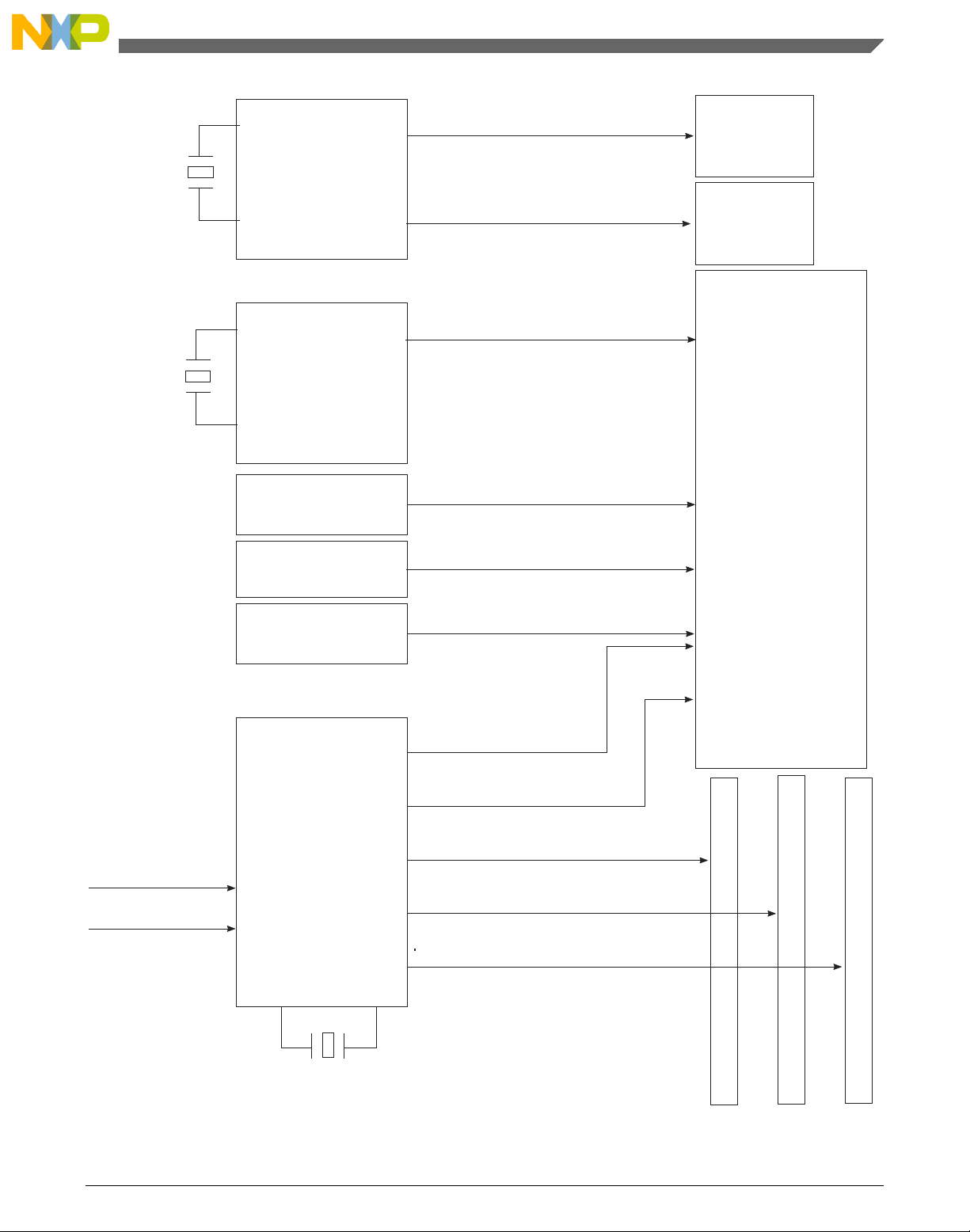
The figure below shows the diagram of T1040RDB platform.
QorIQ T1040 Reference Design Board User Guide, Rev. 0, 06/2015
34 Freescale Semiconductor, Inc.
Page 35

Chapter 2 Architecture
Figure 2-19. T1040RDB
2.17.1 Connectors
The table below lists the various connectors on the T1040RDB platform.
Table 2-7. Connector on board
Reference Designators Used For Notes
J1 UDIMM
J3 COP/JTAG Used for debugging T1040
J5 SD card
J13(2 ports) UART
Table continues on the next page...
QorIQ T1040 Reference Design Board User Guide, Rev. 0, 06/2015
Freescale Semiconductor, Inc. 35
Page 36

Connectors, headers, jumper, push buttons and LED
Table 2-7. Connector on board (continued)
J14(2 ports) Ethernet ports RGMII -> Copper
J15 (4 ports) Ethernet ports QSGMII -> Copper
J18 PCIe x4 Card Intended use is for PCIe cards that are
25 W or less
J19,J20 Mini-PCIe cards
J21 SATA
J22,J23 FXS ports
J24 FXO port
J30 Battery Holder
J34 CPU fan
J37 ATX power
J41 Dual Type A USB
J42 Ethernet port SGMII -> Copper
J43 TDM Riser card
J33,J44-J46 Case fan
2.17.2 Headers
The below table lists the various headers on the T1040RDB platform.
Table 2-8. Header on Board
Reference Designators Used For Notes
J26 Altera CPLD Header Used for programming the Altera CPLD
device
J28 IR36021 Header Used for programming IR36021
2.17.3 Jumper
The below table describes how jumpers are used on the T1040RDB platform:
Table 2-9. Jumper on board
Reference designator Description Status 1 Status 2
J9 PROG_SFP selection Mounted : Fuse Programming Un-mounted : normally
operate (default setting)
J10 PROG_MTR selection Mounted : Fuse Programming Un-mounted : normally
operate (default setting)
Table continues on the next page...
QorIQ T1040 Reference Design Board User Guide, Rev. 0, 06/2015
36 Freescale Semiconductor, Inc.
Page 37

Chapter 2 Architecture
Table 2-9. Jumper on board (continued)
J11 FA_VAL selection - Un-mounted : normally
operate (default setting)
J27 NOT Used - -
2.17.4 Push buttons
The table below describes how the push button is used on the T1040RDB platform.
Table 2-10. Button on board
Reference Designators Used for Notes
SW4 Reset Used to reset the whole board
SW5 Power on/off Used to power on or off the board
2.17.5 LEDs
The table below lists all the LEDs on the T1040RDB board.
Table 2-11. LEDs on board
LED
3.3 V power
supply LED
Status LED D43 Green Status CPLD
FXS1 LED D38 Green FXS1 CPLD
FXS2 LED D39 Green FXS2 CPLD
FXS3 LED D41 Green FXS3 CPLD
FXS4 LED D42 Green FXS4 CPLD
FXO LED D40 Green FXO CPLD
T1040/T1020
LED
T2081 LED D6 Green Detects onboard device CPLD
Part identifier
D44 Green Power on +3.3 V power rail
D5 Green Detects onboard device CPLD
Color
Used for Controlled by
2.18 Temperature
QorIQ T1040 Reference Design Board User Guide, Rev. 0, 06/2015
Freescale Semiconductor, Inc. 37
Page 38

I2C Bus
T1
040
TEMP_ANODE
Thermal sensor
(ADT7461)
DXP1
DXN
TEMP_CATHODE
THERM
ALERT/THERM2
OVER ALARM
THERM ALARM
CPLD
PWM
FAN_Power
DIP switch definition
The T1040 has a thermal diode attached to the die, allowing direct temperature
measurement. These pins are connected to an ADT7461 2-channel thermal monitor,
which allows direct reading of the temperature of the die and is accurate to ±1° C. The
second channel of the ADT7461 measures the ambient (board) temperature. The
ADT7461 temperature warning and alarm signals are connected to the CPLD for
monitoring. The CPLD or user software may use these signals to adjust CPU FAN speed
to protect the CPU from over-temperature failure.
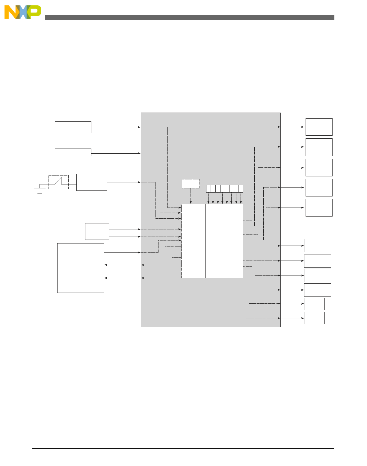
2.19 DIP switch definition
The T1040RDB card has user selectable switches, for evaluating different boot
configurations and other special configurations for this device. The CPLD allows
software to override the configuration pins; for example, when the board is in a board
farm. In order to use the CPLD override option, software sets an override bit that allows
the CPLD to override the switch setting during reset.
38 Freescale Semiconductor, Inc.
Figure 2-20. Thermal Sensor connection
QorIQ T1040 Reference Design Board User Guide, Rev. 0, 06/2015
Page 39

T1040
POR & Override
CPLD Register
CPLD
cfg_xxx
switch
Figure 2-21. CPLD and DIP switch connection
The table below shows how POR configuration is done through switches.
Chapter 2 Architecture
NOTE
0 and 1 are represented by ON and OFF respectively on the
board.
NOTE
The recommended value for the switch settings for NOR flash
is below. Refer this for value of reserved switches:
SW1: 0001 0011
SW2: 1011 1011
SW3: 1110 0001
Table 2-12. POR configuration through switches
Switch Signal name Pin Name Signal meaning Setting
SW1[1:8] cfg_rcw_src[0:7] IFC_AD[8:15] Reset Configuration
SW2[1] cfg_rcw_src[8] IFC_CLE Reset Configuration
SW2[2] cfg_ifc_te IFC_TE IFC external transceiver
SW2[3] cfg_pll_config_sel_b IFC_A18 Reserved Reserved
SW2[4] cfg_por_ainit IFC_A19 Reserved Reserved
word source
word source
enable polarity select
Detail description see
T1040 RM
Detail description see
T1040 RM
0: IFC drives logic 1 for
TE assertion
1: IFC drives logic 0 for
TE assertion
Table continues on the next page...
QorIQ T1040 Reference Design Board User Guide, Rev. 0, 06/2015
Freescale Semiconductor, Inc. 39
Page 40

DIP switch definition
Table 2-12. POR configuration through switches
(continued)
SW2[5:6] cfg_svr[0:1] IFC_A[16:17] Reserved Reserved
SW2[7] cfg_dram_type IFC_A21 DRAM type selection 0: DDR4(1.2V)
1: DDR3L(1.35V)
SW2[8] cfg_rsp_dis IFC_AVD Reserved Reserved
SW3[1] cfg_eng_use0 IFC_WE0 Sys_clock selection 0: differential sys_clk is
selected
1:single sys_clk is
selected
SW3[2:3] cfg_eng_use[1:2] Reserved Reserved Reserved
SW3[4] BOOT_FLASH_SEL - Boot flash selection 0: NOR Flash
1: NAND Flash
SW3[5:7] CFG_VBANK[0:2] - Flash bank select 0: Default
SW3[8] TEST_SEL_N TEST_SEL_B - 0: T1020
1: T1040
1. For SW3[4] : BOOT_FLASH_SEL, it can act as boot flash selection. When BOOT_FLASH_SEL=0, NOR Flash is boot
flash, when BOOT_FLASH_SEL=1, NAND Flash is boot flash.
2. SW3[5:7] can be used to change the staring address for the memory banks. For example, the NOR FLASH memory is
divided into eight memory banks with 16MB size each. Eight different U-Boot image can be programmed into each
memory bank, though normally only settings for bank 0 and bank 4 are used. When NOR FLASH is selected as boot flash
(CS0 is connected to NOR FLASH by setting SW3[4] to ON, RCW[0:8] is set to 0_0111_xxxx using SW1[1:8] and SW2[1]),
a different U-Boot image can be selected to boot up the board, by setting SW3[5:7].
For other boot sources configured by the DIP switch, see the QorIQ T1040 Reference Manual (T1040RM).
1
2
QorIQ T1040 Reference Design Board User Guide, Rev. 0, 06/2015
40 Freescale Semiconductor, Inc.
Page 41

Chapter 3
CPLD specification
This section explains how to program CPLD and provide details about the CPLD
memory map.
3.1 CPLD programming
To program CPLD:
Connect Altera USB-blaster to the CPLD header.
1.
2. Run altera\61\quartus\bin\quartus.exe to open Quartus II.
3. Select Tools->Programmer from the menu bar.
QorIQ T1040 Reference Design Board User Guide, Rev. 0, 06/2015
Freescale Semiconductor, Inc. 41
Page 42

CPLD programming
4. Click the Hardware Setup button to find the USB-blaster connected to the PC.
QorIQ T1040 Reference Design Board User Guide, Rev. 0, 06/2015
42 Freescale Semiconductor, Inc.
Page 43

5. Switch on the board, click Auto Detect to detect EPM240.
Chapter 3 CPLD specification
6. Right-click EPM240, select Change File from the context menu and find the *.pof
file.
7. Select Program/Configure, Verify, Blank-Check checkboxes.
QorIQ T1040 Reference Design Board User Guide, Rev. 0, 06/2015
Freescale Semiconductor, Inc. 43
Page 44

CPLD memory map
8. Click Start. The 100% status on the progress bar indicates that the CPLD is
programmed successfully.
3.2 CPLD memory map
memory map
Offset
address
(hex)
0 Chip ID1 register (CHIPID1) 8 R 55h 3.2.1/44
1 Chip ID2 register (CHIPID2) 8 R AAh 3.2.2/45
2 Hardware version register (HWVER) 8 R See section 3.2.3/45
3 Software version register (SWVER) 8 R See section 3.2.4/46
10 Reset control register (RSTCON1) 8 w1c See section 3.2.5/46
11 Reset control register (RSTCON2) 8 w1c See section 3.2.6/47
12 INTSR 8 R See section 3.2.7/48
13 Flash control and status register (FLHCSR) 8 R/W See section 3.2.8/49
14 Fan control and status register (FANCSR) 8 R/W 3.2.9/49
15 Panel LED control and status register (LEDCSR) 8 R/W See section 3.2.10/50
16 SFP+ control and status register (SFPCSR) 8 R/W 00h 3.2.11/51
17 Miscellaneous control and status register (MISCCSR) 8 R/W See section 3.2.12/51
18 Boot configuration override register (BOOTOR) 8 R/W See section 3.2.13/52
19 Boot configuration register 1 (BOOTCFG1) 8 R/W See section 3.2.14/52
1A Boot configuration register 2 (BOOTCFG2) 8 R/W See section 3.2.15/52
Register name
Width
(in bits)
Access Reset value
Section/
page
QorIQ T1040 Reference Design Board User Guide, Rev. 0, 06/2015
44 Freescale Semiconductor, Inc.
Page 45

3.2.1 Chip ID1 register (CHIPID1 )
Address: 0h base + 0h offset = 0h
Bit 0 1 2 3 4 5 6 7
Read CHIPID1
Write
Reset
0 1 0 1 0 1 0 1
CHIPID1 field descriptions
Field Description
0–7
CHIPID1
0x55, Identification of the CPLD image.
3.2.2 Chip ID2 register (CHIPID2)
Chapter 3 CPLD specification
Address: 0h base + 1h offset = 1h
Bit 0 1 2 3 4 5 6 7
Read CHIPID2
Write
Reset
1 0 1 0 1 0 1 0
CHIPID2 field descriptions
Field Description
0–7
CHIPID2
0xaa, Identification of the CPLD image.
3.2.3 Hardware version register (HWVER)
Address: 0h base + 2h offset = 2h
Bit 0 1 2 3 4 5 6 7
Read HW_VER
Write
Reset
n* n* n* n* n* n* n* n*
* Notes:
HW_VER field: n=Depends on PLD image revision•
QorIQ T1040 Reference Design Board User Guide, Rev. 0, 06/2015
Freescale Semiconductor, Inc. 45
Page 46

CPLD memory map
HWVER field descriptions
Field Description
0–7
HW_VER
The version field of the hardware board.
3.2.4 Software version register (SWVER)
Address: 0h base + 3h offset = 3h
Bit 0 1 2 3 4 5 6 7
Read SW_VER
Write
Reset
* Notes:
SW_VER field: n=Depends on PLD image version•
n* n* n* n* n* n* n* n*
SWVER field descriptions
Field Description
0–7
SW_VER
The version field of the CPLD software.
3.2.5 Reset control register (RSTCON1)
Address: 0h base + 10h offset = 10h
Bit 0 1 2 3 4 5 6 7
Read SW_RST
Write w1c w1c w1c w1c
Reset
Field Description
0
SW_RST
1
2
EC1_RST
3
EC2_RST
0 0 0 0 0 0 0 0
0: No reset occurs.
1: Writing logic 1 will produce whole board reset# signal, this bit can auto clear.
This field is reserved.
0: No reset occurs.
1: Write a logic 1 produces RGMII PHY1(RTL82111E-VB) reset# signal, this bit can auto clear.
0: No reset occurs.
1: Writing logic 1 produces RGMII PHY2(RTL82111E-VB) reset# signal, this bit can auto clear.
Reserved
EC1_RST EC2_RST SG_RST QSG1_RST QSG2_RST XG_RST
RSTCON1 field descriptions
w1c w1c
w1c
Table continues on the next page...
QorIQ T1040 Reference Design Board User Guide, Rev. 0, 06/2015
46 Freescale Semiconductor, Inc.
Page 47

RSTCON1 field descriptions (continued)
Field Description
4
SG_RST
5
QSG1_RST
6
QSG2_RST
7
XG_RST
0: No reset occurs.
1: Writing logic 1 produces SGMII PHY(RTL82111DN) reset# signal, this bit can auto clear.
0: No reset occurs.
1: Writing logic 1 produces QSGMII PHY(VSC8514) reset# signal, this bit can auto clear.
0: No reset occurs.
1: Writing logic 1 produces 10G PHY(CS4315) reset# signal, this bit can auto clear.
0: No reset occurs
1: Writing logic 1 produces 10G PHY (CS4315)reset# signal, this bit can auto clear.(Bit 7 needs to go)
3.2.6 Reset control register (RSTCON2)
Address: 0h base + 11h offset = 11h
Bit 0 1 2 3 4 5 6 7
Read
Write
Reset
Reserved
0 0 0 0 0 0 0 0
TDMR_RST PEX_RST
w1c
Chapter 3 CPLD specification
MPEX1_
RST
w1c
w1c w1c
MPEX2_
RST
RSTCON2 field descriptions
Field Description
0–3
4
TDMR_RST
5
PEX_RST
6
MPEX1_RST
7
MPEX2_RST
This field is reserved.
0: No reset occurs.
1: Writing logic 1 produces TDM riser card reset# signal, this bit can auto clear.
0: No reset occurs.
1: Writing logic 1 produces PCIe x4 slot reset# signal, this bit can auto clear.
0: No reset occurs.
1: Writing logic 1 produces miniPCIe card1 reset# signal, this bit can auto clear.
0: No reset occurs
1: Writing logic 1 produces miniPCIe card2 reset# signal, this bit can auto clear.
QorIQ T1040 Reference Design Board User Guide, Rev. 0, 06/2015
Freescale Semiconductor, Inc. 47
Page 48

CPLD memory map
3.2.7 INTSR
Address: 0h base + 12h offset = 12h
Bit 0 1 2 3 4 5 6 7
Read THERM_INT SG_INT QSG1_INT QSG2_INT POTSA_INT POTSB_INT TDMR1_INT TDMR2_INT
Write
Reset
* Notes:
TDMR2_INT field: Depends on PLD image revision.•
TDMR1_INT field: Depends on PLD image revision.•
POTSB_INT field: Depends on PLD image revision.•
POTSA_INT field: Depends on PLD image revision.•
QSG2_INT field: Depends on PLD image revision.•
QSG1_INT field: Depends on PLD image revision.•
SG_INT field: Depends on PLD image revision.•
THERM_INT field: Depends on PLD image revision.•
n* n* n* n* n* n* n* n*
INTSR field descriptions
Field Description
0
THERM_INT
1
SG_INT
2
QSG1_INT
3
QSG2_INT
4
POTSA_INT
5
POTSB_INT
6
TDMR1_INT
7
TDMR2_INT
0: No interrupt occurs.
1: Board over temperature interrupt occurs.
0: No interrupt occurs.
1: SGMII PHY(RTL8211DN) interrupt occurs
0: No interrupt pending
1: QSGMII PHY1(VSC8514) interrupt occurs.
0: No interrupt pending
1: QSGMII PHY2(VSC8514) interrupt occurs
0: No interrupt pending
1: POTS A interrupt occurs
0: No interrupt pending
1: POTS B interrupt occurs.
0: No interrupt pending
1: TDM riser card interrupt 1 occurs.
0: No interrupt pending
1: TDM riser card interrupt 2 occurs.
QorIQ T1040 Reference Design Board User Guide, Rev. 0, 06/2015
48 Freescale Semiconductor, Inc.
Page 49

3.2.8 Flash control and status register (FLHCSR)
Address: 0h base + 13h offset = 13h
Bit 0 1 2 3 4 5 6 7
Read BOOT_SEL
Write
Reset
n 0 n n n 0 0 0
BANK_OR
SW_BANK_
SEL0
FLHCSR field descriptions
Field Description
0
BOOT_SEL
1
BANK_OR
2
SW_BANK_SEL0
3
SW_BANK_SEL1
4
SW_BANK_SEL2
5
BANK_SEL0
6
BANK_SEL1
7
BANK_SEL2
0: Boot from 16-bit NOR flash.
1: Boot from 8-bit NAND flash.
0: NOR flash bank select from CPLD override disable.
1: NOR flash bank select from CPLD override enable.
NOR flash bank select bit0 of switch status is 0.
1: NOR flash bank select bit0 of switch status is 1.
0: NOR flash bank select bit1 of switch status is 0.
1: NOR flash bank select bit1 of switch status is 1.
0: NOR flash bank select bit2 of switch status is 0.
1: NOR flash bank select bit2 of switch status is 1.
0: NOR flash bank select bit0 set 0.
1: NOR flash bank select bit0 set 1.
0: NOR flash bank select bit1 set 0.
1: NOR flash bank select bit1 set 1
0: NOR flash bank select bit2 set 0.
1: NOR flash bank select bit2 set 1.
SW_BANK_
SEL1
SW_BANK_
SEL2
BANK_
SEL0
Chapter 3 CPLD specification
BANK_
SEL1
BANK_
SEL2
3.2.9 Fan control and status register (FANCSR)
Address: 0h base + 14h offset = 14h
Bit 0 1 2 3 4 5 6 7
Read
Write
Reset
QorIQ T1040 Reference Design Board User Guide, Rev. 0, 06/2015
Freescale Semiconductor, Inc. 49
Reserved FAN_PWM
Page 50

CPLD memory map
FANCSR field descriptions
Field Description
0–3
-
4–7
FAN_PWM
This field is reserved.
0000: PWM duty cycle is 0%, fan stop running.
0001~1110: PWM duty cycle is 6.7%~93.3%, fan speed control.
1111: PWM duty cycle is 100%, fan full speed.
3.2.10 Panel LED control and status register (LEDCSR )
Address: 0h base + 15h offset = 15h
Bit 0 1 2 3 4 5 6 7
Read
Write
Reset
STS_LED FXS1_LED FXS2_LED FXS3_LED FXS4_LED FXO_LED
0 0 0 0 0 0 n n
XG_LED1 XG_LED2
LEDCSR field descriptions
Field Description
0
STS_LED
1
FXS1_LED
2
FXS2_LED
3
FXS3_LED
4
FXS4_LED
5
FXO_LED
6
XG_LED1
7
XG_LED2
0: Panel STATUS LED off.
1: Panel STATUS LED on.
0: Panel FXS1 LED off
1: Panel FXS1 LED on
0: Panel FXS2 LED off
1: Panel FXS2 LED on
0: Panel FXS3 LED off
10: Panel FXS3 LED on
0: Panel FXS4 LED off
1: Panel FXS4 LED on
0: Panel FXO LED off
1: Panel FXO LED on
0: Panel XG TX LED off when SFP+ not present or TX disabled
1: Panel XG TX LED on when SFP+ present and TX enabled
0: Panel XG RX LED off when SFP+ not present or RX los.
1: Panel XG RX LED on when SFP+ present and RX optical received
QorIQ T1040 Reference Design Board User Guide, Rev. 0, 06/2015
50 Freescale Semiconductor, Inc.
Page 51

Chapter 3 CPLD specification
3.2.11 SFP+ control and status register (SFPCSR )
Address: 0h base + 16h offset = 16h
Bit 0 1 2 3 4 5 6 7
Read
Write
Reset
0 0 0 0 0 0 0 0
Reserved
SFPCSR field descriptions
Field Description
0–7
-
This field is reserved.
3.2.12 Miscellaneous control and status register (MISCCSR )
Address: 0h base + 17h offset = 17h
Bit 0 1 2 3 4 5 6 7
Read
Write
Reset
SPI_CS3_
SEL
0 0 1 1 0 n n n
SLEEP_EN REQ_MD
MISCCSR field descriptions
Field Description
0
SPI_CS3_SEL
1
SLEEP_EN
2–3
REQ_MD
4
TDMR_PRS
5
PEX_PRS
6
T2081_DET
7
TEST_SEL_N
0: SPI_CS3 select TDMR SPI CS0
1: SPI_CS3 select TDMR SPI CS1
Before entering deep sleep mode, set ‘1’ to this bit, after exiting deep sleep mode, set ‘0’ to this bit
0 Normal operation
1 Deep sleep enable bit
00 No reset occurs when HRESET_REQ triggered.
01 HRESET occurs when HRESET_REQ triggered.
10 Reserved
11 PORESET occurs when HRESET_REQ triggered.
0: TDM riser card not present
1: TDM riser card present
0 PCIe card not present in x4 slot.
1 PCIe card present in x4 slot.
0: T1040 on board
1: T2081 on board
0: TEST_SEL_N pin status is 0
1: TEST_SEL_N pin status is 1
TDMR_PRS PEX_PRS T2081_DET
TEST_SEL_
N
QorIQ T1040 Reference Design Board User Guide, Rev. 0, 06/2015
Freescale Semiconductor, Inc. 51
Page 52

CPLD memory map
3.2.13 Boot configuration override register (BOOTOR)
Address: 0h base + 18h offset = 18h
Bit 0 1 2 3 4 5 6 7
Read
Write
Reset
BOOTOR field descriptions
Field Description
0–6
7
BOOT_OR
This field is reserved.
0: Boot configuration from CPLD override disable
1: Boot configuration from CPLD override enable
Reserved BOOT_OR
3.2.14 Boot configuration register 1 (BOOTCFG1 )
Address: 0h base + 19h offset = 19h
Bit 0 1 2 3 4 5 6 7
Read
Write
Reset
cfg_rcw_src[0:7]
BOOTCFG1 field descriptions
Field Description
0–7
cfg_rcw_src[0:7]
NOTE:
For more information, see QorIQ T1040, T1020 Data Sheet.
3.2.15 Boot configuration register 2 (BOOTCFG2)
NOTE
For more information, refer T1040 datasheet.
Address: 0h base + 1Ah offset = 1Ah
Bit 0 1 2 3 4 5 6 7
Read
Write
Reset
cfg_rcw_
src8
Reserved cfg_svr[0:1] Reserved cfg_eng_use[0:2]
QorIQ T1040 Reference Design Board User Guide, Rev. 0, 06/2015
52 Freescale Semiconductor, Inc.
Page 53

BOOTCFG2 field descriptions
Field Description
0
cfg_rcw_src8
1
-
2–3
cfg_svr[0:1]
4
-
5–7
cfg_eng_use[0:2]
RCW source bit 8.
This field is reserved.
cfg_svr bit for T1040 Power-on-reset use
This field is reserved.
cfg_eng_use bit for T1040 Power-on-reset use.
Chapter 3 CPLD specification
QorIQ T1040 Reference Design Board User Guide, Rev. 0, 06/2015
Freescale Semiconductor, Inc. 53
Page 54

CPLD memory map
QorIQ T1040 Reference Design Board User Guide, Rev. 0, 06/2015
54 Freescale Semiconductor, Inc.
Page 55

Chapter 4
Software configuration
This section explains:
• Preparing board
• Ethernet port map
• NOR flash image layout
• Switch settings
• SDK Build details
• Flashing and updating images
4.1 Preparing board
The figure below shows the front panel of the T1040 RDB.
Figure 4-1. T1040RDB front panel
To prepare the T1040RDB for use, default configuration should be: CPU: 1.4 GHz,
DDR: 1600 MT/s. The steps are:
Attach an RS-232 cable between the T1040RDB UART0 port and host computer
1.
2. Open a serial console tool on the host computer to communicate with the T1040RDB
3. Configure the host computer's serial port with the following settings:
• Data rate: 115200 bps
• Number of data bits: 8
• Parity: None
• Number of stop bits: 1
• Flow control: Hardware/None
QorIQ T1040 Reference Design Board User Guide, Rev. 0, 06/2015
Freescale Semiconductor, Inc. 55
Page 56

Preparing board
Push the power button on the front side of the chassis. The board will boot and show the
U-Boot console messages, similar to the following.
U-Boot 2014.01QorIQ-SDK-T1040-BSP0.2 (Mar 07 2014 - 01:04:58)
CPU0: T1040E, Version: 1.0, (0x85280010)
Core: e5500, Version: 2.0, (0x80241020)
Clock Configuration:
CPU0:1400 MHz, CPU1:1400 MHz, CPU2:1400 MHz, CPU3:1400 MHz,
CCB:600 MHz,
DDR:800 MHz (1600 MT/s data rate) (Asynchronous), IFC:150 MHz
FMAN1: 600 MHz
QMAN: 300 MHz
PME: 300 MHz
L1: D-cache 32 KiB enabled
I-cache 32 KiB enabled
Reset Configuration Word (RCW):
00000000: 0c18000e 0e000000 00000000 00000000
00000010: 66000002 80000002 ec027000 01000000
00000020: 00000000 00000000 00000000 00032810
00000030: 00000000 0342500f 00000000 00000000
Board: T1040RDB
Board rev: 0x01 CPLD ver: 0x06, vBank: 0
I2C: ready
SPI: ready
DRAM: Initializing....using SPD
Detected UDIMM 18KSF51272AZ-1G6K1
2 GiB left unmapped
DDR: 4 GiB (DDR3, 64-bit, CL=11, ECC on)
DDR Chip-Select Interleaving Mode: CS0+CS1
Flash: 256 MiB
L2: 256 KiB enabled
Corenet Platform Cache: 256 KiB enabled
Using SERDES1 Protocol: 102 (0x66)
NAND: 1024 MiB
MMC: FSL_SDHC: 0
PCIe1: Root Complex, no link, regs @ 0xfe240000
PCIe1: Bus 00 - 00
PCIe2: Root Complex, x1 gen1, regs @ 0xfe250000
02:00.0 - 8086:10d3 - Network controller
PCIe2: Bus 01 - 02
PCIe3: Root Complex, no link, regs @ 0xfe260000
PCIe3: Bus 03 - 03
PCIe4: Root Complex, no link, regs @ 0xfe270000
PCIe4: Bus 04 - 04
In: serial
Out: serial
Err: serial
Net: Initializing Fman
Fman1: Uploading microcode version 106.4.14
FSL_MDIO0:0 is connected to FM1@DTSEC1. Reconnecting to FM1@DTSEC2
FSL_MDIO0:0 is connected to FM1@DTSEC2. Reconnecting to FM1@DTSEC3
e1000: 68:05:ca:04:d5:6a
FM1@DTSEC1, FM1@DTSEC2, FM1@DTSEC3, FM1@DTSEC4 [PRIME], FM1@DTSEC5, e1000#0
Warning: e1000#0 MAC addresses don't match:
Address in SROM is 68:05:ca:04:d5:6a
Address in environment is 00:04:9f:ef:00:00
Hit any key to stop autoboot: 0
The system auto boots and shows the following Linux login screen.
t1040rdb
login: root
root@t1040rdb:~#
QorIQ T1040 Reference Design Board User Guide, Rev. 0, 06/2015
56 Freescale Semiconductor, Inc.
Page 57

Chapter 4 Software configuration
4.2 Ethernet port map
The table below shows how Ethernet ports match to Linux, U-Boot, and the front-panel
label on the 1U box.
Table 4-1. Ethernet mapping table
Label on 1U
box
Internal port FM1@DTSEC1
Internal port FM1@DTSEC2
ETH0 FM1@DTSEC4 fm1-gb3 0xfe4e6000 RGMII
ETH1 FM1@DTSEC5 fm1-gb4 0xfe4e8000 RGMII
ETH2 FM1@DTSEC3 fm1-gb2 0xfe4e4000 SGMII
ETH3 Not supported in U-Boot 0xfe4e0000 L2 switch
ETH4 Not supported in U-Boot L2 switch
ETH5 Not supported in U-Boot L2 switch
ETH6 Not supported in U-Boot L2 switch
ETH7 Not supported in U-Boot 0xfe4e2000 L2 switch
ETH8 Not supported in U-Boot L2 switch
ETH9 Not supported in U-Boot L2 switch
ETH10 Not supported in U-Boot L2 switch
1. Connected to L2 switch port at 2.5 Gbit/s. This port cannot be connected to external PHYs, as T1040RDB supports only
SerDes protocol, 0x66
Port in U-Boot Port in Linux FMan address Type
1
1
fm1-gb0
fm1-gb1
NOTE
ETH3-ETH10 belong to the switch. They are not visible as
interfaces in Linux. Switch control software is required to
control them.
4.3 NOR flash image layout
NOR flash can be divided into two flash banks (0 and 4) to store a main image and an
alternative backup image. This is shown in the below table.
QorIQ T1040 Reference Design Board User Guide, Rev. 0, 06/2015
Freescale Semiconductor, Inc. 57
Page 58

Switch settings
Table 4-2. Image layout in NOR flash
Start address End address Image Max size
0xEFF40000 0xEFFFFFFF U-Boot (current bank) 768KB
0xEFF20000 0xEFF3FFFF U-Boot env (current bank) 128KB
0xEFF10000 0XEFF1FFFF QUICC Engine microcode (current bank) 64KB
0xEFF00000 0xEFF0FFFF FMan microcode (current bank) 64KB
0xED300000 0xEFEFFFFF rootfs (alternative bank) 43MB
0xEC800000 0xEC8FFFFF Hardware device tree (alternative bank) 1MB
0xEC020000 0XEC7FFFFF Linux.uImage (alternative bank) 7MB+875KB
0xEC000000 0XEC01FFFF RCW (alternative bank) 7MB+875KB
0xEBF40000 0XEBFFFFFF U-Boot (alternative bank) 768KB
0xEBF20000 0XEBF3FFFF U-Boot env (alternative bank) 128KB
0xEBF10000 0XEBF1FFFF QUICC Engine microcode (alt bank) 64KB
0XEBF00000 0XEBF0FFFF FMan microcode (alternative bank) 64KB
0xE9300000 0XEBEFFFFF rootfs (current bank) 43MB
0XE8800000 0XE88FFFFF Hardware device tree (current bank) 1MB
0xE8020000 0xE86FFFFF Linux.uImage (current bank) 7MB+875KB
0xE8000000 0xE801FFFF RCW (current bank) 128KB
4.4 Switch settings
This chapter defines the default switch settings and other boot source settings.
NOTE
You may find slightly different default switch settings,
depending on the SDK being used; check the relevant
information.
4.4.1 Switch default settings (NOR flash boot)
This section defines the default switch settings for NOR flash boot.
NOTE
ON and OFF are being represented as 0 and 1 respectively, on
the board.
QorIQ T1040 Reference Design Board User Guide, Rev. 0, 06/2015
58 Freescale Semiconductor, Inc.
Page 59

Chapter 4 Software configuration
DIP Switch
binary
value
SW1 0001 0011 ON ON ON OFF ON ON OFF OFF
SW2 1011 1011 OFF ON OFF OFF OFF ON OFF OFF
SW3 1110 0001 OFF OFF OFF ON ON ON ON OFF
1 2 3 4 5 6 7 8
4.4.2 Other boot source settings
This section defines the settings for NAND boot, SPI boot SW, and SD boot.
NAND boot settings:
DIP Switch
binary
value
SW1 1000 1000 OFF ON ON ON OFF ON ON ON
SW2 0011 1011 ON ON OFF OFF OFF ON OFF OFF
SW3 1111 0001 OFF OFF OFF OFF ON ON ON OFF
1 2 3 4 5 6 7 8
SPI boot SW settings:
DIP Switch
binary
value
SW1 0010 0010 ON ON OFF ON ON ON OFF ON
SW2 1011 1011 OFF ON OFF OFF OFF ON OFF OFF
SW3 1110 0001 OFF OFF OFF ON ON ON ON OFF
1 2 3 4 5 6 7 8
SD boot settings:
DIP Switch
binary
value
SW1 0010 0000 ON ON OFF ON ON ON ON ON
SW2 0011 1011 ON ON OFF OFF OFF ON OFF OFF
SW3 1110 0001 OFF OFF OFF ON ON ON ON OFF
1 2 3 4 5 6 7 8
4.4.3 Switch detailed description
QorIQ T1040 Reference Design Board User Guide, Rev. 0, 06/2015
Freescale Semiconductor, Inc. 59
Page 60

SDK Build details
For a detailed switch default description, see Table 2-12
4.5 SDK Build details
For information on build details, see the SDK documentation.
4.6 Flashing and updating images
This section explains:
• Flashing images on NOR flash and booting from NOR Flash
• Flashing eSPI boot images
• Booting Linux
4.6.1 Flashing images on and booting from NOR flash
Onboard Images can be updated as mentioned below. On board re-start, the board should
boot with new images. For information about switch settings, see Switch settings
• RCW programming on current bank (from U-Boot prompt)
For T1040RDB, use rcw/t1040rdb/RR_P_66/ rcw_1400MHz.bin
NOTE
This RCW can change depending upon the requirements
=> tftp 1000000 <rcw>.bin
=> protect off all
=> erase 0xe8000000 0xe801ffff
=> cp.b 0x1000000 0xe8000000 $filesize
• FMan microcode programming on current bank (from U-Boot prompt)
=> tftp 0x3000000 <fsl_fman_ucode>.bin
=> protect off all
Un-Protect Flash Bank # 1
=> erase 0xEFF00000 eff1ffff
. done
Erased 1 sectors
=> cp.b 3000000 0xEFF00000 10000
Copy to Flash...
9....8....7....6....5....4....3....2....1....done
• U-Boot binary programming on current bank (from U-Boot prompt)
=> tftp 0x1000000 u-boot.bin
QorIQ T1040 Reference Design Board User Guide, Rev. 0, 06/2015
60 Freescale Semiconductor, Inc.
Page 61

Chapter 4 Software configuration
=> protect off all
Un-Protect Flash Bank # 1
=> erase 0xeff40000 0xefffffff
.... done
Erased 4 sectors
=> cp.b 0x1000000 0xeff40000 0xc0000
Copy to Flash...
9....8....7....6....5....4....3....2....1....done
• RCW programming on alternate bank (from U-Boot prompt)
For T1040RDB, use rcw/t1040rdb/RR_P_66/ rcw_1400MHz.bin
NOTE
This RCW can change depending upon the requirements.
=> tftp 1000000 <rcw>.bin
=> protect off all
=> erase 0xec000000 0xec01ffff
=> cp.b 0x1000000 0xec000000 $filesize
• FMan microcode programming on alternate bank (from U-Boot prompt)
=> tftp 0x3000000 <fsl_fman_ucode>.bin
=> protect off all
Un-Protect Flash Bank # 1
=> erase 0xebf00000 ebf1ffff
. done
Erased 1 sectors
=> cp.b 3000000 0xebf00000 10000
Copy to Flash...
9....8....7....6....5....4....3....2....1....done
• U-Boot binary programming on alternate bank (from U-Boot prompt)
=> tftp 0x1000000 u-boot.bin
=> protect off all
Un-Protect Flash Bank # 1
=> erase 0xebf40000 0xebffffff
.... done
Erased 4 sectors
=> cp.b 0x1000000 0xebf40000 0xc0000
Copy to Flash...
9....8....7....6....5....4....3....2....1....done
4.6.2 Flashing eSPI boot images
The steps for flashing and updating images for eSPI are as follows:
Write PBL1.bin (created using QCS tool) at offset 0:
1.
QorIQ T1040 Reference Design Board User Guide, Rev. 0, 06/2015
Freescale Semiconductor, Inc. 61
Page 62

Flashing and updating images
=>tftp 100000 PBL1.bin
=>sf probe 0
=>sf erase 0 100000
=>sf write 100000 0 $filesize
2. Write u-boot.bin at offset 0x40000 (256 KB):
=>tftp 100000 u-boot.bin
=>sf write 100000 40000 $filesize
3. Write FMan microcode to eSPI from offset 0x110000:
=>tftp 100000 fsl_fman_ucode_xx.bin
=>sf erase 110000 10000
=>sf write 100000 110000 $filesize
4. Shut down the board.
5. Change board switch configuration for eSPI boot.
6. Switch on the board.
NOTE
For more information about building U-Boot images,
generating PBL images, see eSPI/SD/NAND boot in SDK
documentation.
4.6.3 Flashing NAND boot images
The steps for flashing and updating images for NAND are as follows:
All operations are done on the target in the U-Boot console.
Write PBL1.bin to NAND from offset 0x0:
1.
=>tftp 100000 PBL1.bin
=>nand info
=>nand erase 0 100000
=>nand write 100000 0 $filesize
2. Write u-boot.bin to NAND from offset 0x40000 (256 KB):
=>tftp 100000 u-boot.bin
=>nand write 100000 40000 $filesize
3. Write FMan microcode to NAND from offset 0x180000:
=>nand info
=>tftp 100000 fsl_fman_ucode_xx.bin
=>nand erase 180000 80000
=>nand write 100000 180000 $filesize
4. Shut down the board.
5. Change board switch configuration for NAND boot.
6. Switch on the board.
QorIQ T1040 Reference Design Board User Guide, Rev. 0, 06/2015
62 Freescale Semiconductor, Inc.
Page 63

Chapter 4 Software configuration
NOTE
For more information about building U-Boot images,
generating PBL images, see eSPI/SD/NAND boot in SDK
documentation.
4.6.4 Flashing SD card boot images
The steps for flashing and updating images for SD card are as follows:
You need to write two images, the first is the PBL1.bin produced by QCS tool, the second
is the u-boot.bin.
Write PBL1.bin at offset block 8:
1.
=>tftp 100000 PBL1.bin
=>mmcinfo
=>mmc write 100000 8 block_number
2. Write u-boot.bin at offset 0x41000 (260KB), for example, 520(0x208) blockes.
=>tftp 100000 u-boot.bin
=>mmc write 100000 208 block_number
3. Write FMan microcode to SD card from block 0x820:
=>tftp 100000 fsl_fman_ucode_xx.bin
=>mmc write 100000 820 block_number
4. Shut down the board.
5. Change board switch configuration for SD boot.
6. Switch on the board.
NOTE
For more information about building U-Boot images,
generating PBL images, see eSPI/SD/NAND boot in SDK
documentation.
4.6.5 Booting Linux
• Setting bootargs and serverip at U-Boot prompt:
=> setenv bootargs "root=/dev/ram rw console=ttyS0,115200
ramdisk_size=700000”
=> setenv ethact FM1@DTSEC4
=> setenv ipaddr <ipaddr>
=> setenv serverip <serverip>
• From U-Boot prompt, for booting Linux with 32-bit configuration on T1040RDB:
=> setenv my_kern 'tftp 0x1000000 <uImage>’
=> setenv my_fs 'tftp 0x2000000 <rfs_e5500.bin>'
QorIQ T1040 Reference Design Board User Guide, Rev. 0, 06/2015
Freescale Semiconductor, Inc. 63
Page 64

Flashing and updating images
=> setenv my_dtb 'tftp 0x00c00000 <t1040rdb.dtb>'
=> setenv my_boot bootm 0x1000000 0x2000000 0x0c00000
=> setenv boot run my_dtb my_fs my_kern my_boot
=> save
=> run boot
• From U-Boot prompt, for booting Linux with 64-bit configuration on T1040RDB:
=> setenv my_kern 'tftp 0x1000000 <uImage_64bit>’
=> setenv my_fs 'tftp 0x2000000 <rfs_e5500.bin>'
=> setenv my_dtb 'tftp 0x00c00000 <t1040rdb.dtb>'
=> setenv my_boot bootm 0x1000000 0x2000000 0x0c00000
=> setenv boot run my_dtb my_fs my_kern my_boot
=> save
=> run boot
QorIQ T1040 Reference Design Board User Guide, Rev. 0, 06/2015
64 Freescale Semiconductor, Inc.
Page 65

Appendix A
Revision History
Table A-1 summarizes revisions to this document.
Table A-1. Revision history
Revision Date Description
0 06/2015 Initial release.
QorIQ T1040 Reference Design Board User Guide, Rev. 0, 06/2015
Freescale Semiconductor, Inc. 65
Page 66

QorIQ T1040 Reference Design Board User Guide, Rev. 0, 06/2015
66 Freescale Semiconductor, Inc.
Page 67

How to Reach Us:
Home Page:
freescale.com
Web Support:
freescale.com/support
Information in this document is provided solely to enable system and
software implementers to use Freescale products. There are no express
or implied copyright licenses granted hereunder to design or fabricate
any integrated circuits based on the information in this document.
Freescale reserves the right to make changes without further notice to
any products herein.
Freescale makes no warranty, representation, or guarantee regarding
the suitability of its products for any particular purpose, nor does
Freescale assume any liability arising out of the application or use of
any product or circuit, and specifically disclaims any and all liability,
including without limitation consequential or incidental damages.
“Typical” parameters that may be provided in Freescale data sheets
and/or specifications can and do vary in different applications, and
actual performance may vary over time. All operating parameters,
including “typicals,” must be validated for each customer application by
customer's technical experts. Freescale does not convey any license
under its patent rights nor the rights of others. Freescale sells products
pursuant to standard terms and conditions of sale, which can be found
at the following address: freescale.com/SalesTermsandConditions.
Freescale and the Freescale logo are trademarks of Freescale
Semiconductor, Inc. Reg. U.S. Pat. & Tm. Off. Flexis and Processor
Expert are trademarks of Freescale Semiconductor, Inc. All other
product or service names are the property of their respective owners.
© 2015 Freescale Semiconductor, Inc. All rights reserved.
Document Number T1040RDBPAUG
Revision 0, 06/2015
Page 68

Mouser Electronics
Authorized Distributor
Click to View Pricing, Inventory, Delivery & Lifecycle Information:
NXP:
T1040D4RDB-PA
 Loading...