

Page 1

QorIQ FRDM-LS1012A Board
Reference Manual
Document Number: FRDM-LS1012ARM
Rev. 3, 12/2016
Page 2

QorIQ FRDM-LS1012A Board Reference Manual, Rev. 3, 12/2016
2 NXP Semiconductors
Page 3

Contents
Section number Title Page
Chapter 1
Overview
1.1 Introduction.....................................................................................................................................................................5
1.2 Related documentation....................................................................................................................................................5
1.3 Acronyms and abbreviations...........................................................................................................................................6
1.4 FRDM-LS1012A features...............................................................................................................................................7
1.5 FRDM-LS1012A block diagram.................................................................................................................................... 8
1.6 FRDM-LS1012A top view............................................................................................................................................. 8
Chapter 2
LS1012AFRDM Functional Description
2.1 Processor.........................................................................................................................................................................11
2.2 Power supplies................................................................................................................................................................ 11
2.2.1 Primary power supply........................................................................................................................................ 12
2.2.2 FRDM-LS1012A power supply delivery system...............................................................................................13
2.2.3 Power-ON.......................................................................................................................................................... 14
2.2.4 Voltage regulation..............................................................................................................................................14
2.3 Reset and configuration signals...................................................................................................................................... 15
2.4 Clocks............................................................................................................................................................................. 17
2.5 Double data rate (DDR) memory....................................................................................................................................18
2.6 Serializer/deserializer (SerDes)...................................................................................................................................... 18
2.7 Ethernet controller.......................................................................................................................................................... 18
2.7.1 SGMII ports....................................................................................................................................................... 18
2.8 Audio interface................................................................................................................................................................21
2.9 USB interface .................................................................................................................................................................21
2.10 I2C ports..........................................................................................................................................................................22
2.10.1 I2C devices and addresses..................................................................................................................................22
2.11 QSPI interface.................................................................................................................................................................23
2.12 SPI interface....................................................................................................................................................................23
QorIQ FRDM-LS1012A Board Reference Manual, Rev. 3, 12/2016
NXP Semiconductors 3
Page 4

Section number Title Page
2.13 Ardiuno........................................................................................................................................................................... 24
2.14 JTAG port....................................................................................................................................................................... 24
2.14.1 CMSIS-DAP...................................................................................................................................................... 24
2.15 GPIO pins........................................................................................................................................................................25
2.16 Temperature ................................................................................................................................................................... 26
2.17 Power-monitoring LEDs.................................................................................................................................................26
2.18 Revision control..............................................................................................................................................................26
QorIQ FRDM-LS1012A Board Reference Manual, Rev. 3, 12/2016
4 NXP Semiconductors
Page 5

Chapter 1
Overview
1.1 Introduction
The QorIQ FRDM-LS1012A board is an ultra-low-cost development platform for
LS1012A. The board provides connectivity support for SPI, UART, and I2C based
Arduino and freedom boards. Also, the FRDM-LS1012A supports the DDR3L memory,
two 1 Gbit/s Ethernet ports, one USB 3.0 5 Gbit/s port, and the Audio in and out
interface. The system is lead-free and RoHS-compliant.
The LS1012A processor is built on the LS architecture combining one ARM® A53
processor core with the datapath acceleration and network, peripheral interfaces required
for networking, wireless infrastructure, and the general-purpose embedded applications.
The FRDM-LS1012A onboard resources and debugging devices allow you to:
• Upload and run code
• Use the FRDM-LS1012A as a demonstration tool
A software application developed for the FRDM-LS1012A can run with various input/
output data streams, such as SGMII, SAI, or USB connections. The board support
package (BSP) is developed using the Linux operating system.
1.2
Related documentation
Table 1-1 lists the additional documents that you can refer to, for more information about
the FRDM-LS1012A.
Some of these documents may be available only under a non-disclosure agreement
(NDA). To request access to these documents, contact your local NXP field applications
engineer or sales representative.
QorIQ FRDM-LS1012A Board Reference Manual, Rev. 3, 12/2016
NXP Semiconductors 5
Page 6
Table 1-1. Related documentation
Document Description
QorIQ FRDM-LS1012A board Getting Started Guide Explains the FRDM-LS1012A settings and physical
connections needed to boot the board.
FRDM-LS1012A Errata Lists and describes all known errata for the FRDM-LS1012A.
It also describes the available workaround for each errata and
their detailed explanation, where necessary.
QorIQ LS1012A Family Reference Manual Provides a detailed description of the LS1012A processor and
of some of its features, such as memory mapping, interfaces,
chip features, and clock information.
QorIQ LS1012A Data Sheet Contains the LS1012A information on pin assignments,
electrical characteristics, package information, and ordering
information.
LS1012A Chip Errata Lists the details of all known silicon errata for LS1012A.
QorIQ LS1012A Design Checklist, AN5192 This document provides recommendations for new designs
based on LS1012A.
This document can also be used to debug newly-designed
systems by highlighting those aspects of a design that merit
special attention during initial system start-up.
1.3 Acronyms and abbreviations
The following table lists the acronyms and abbreviations used in this document.
Table 1-2. Acronyms and abbreviations
Term Description
DDR Double Data Rate
DRAM Dynamic random-access memory
DUART Dual universal asynchronous receiver/transmitter
DUT Device Under Test
FET Field-effect transistor
GPIO General-purpose input/output
I2C Inter-Integrated Circuit Multi-Master Serial Computer Bus
JTAG Joint Test Action Group (IEEE 1149.1 standard)
LDO Low-dropout
OTG On-The-Go
PLL Phased Lock Loop
PS Power supply
PSU Power supply unit
RCW Reset Configuration Word
SDA Serial data line
SerDes Serializer/deserializer used to interface with serial interfaces, such as PCIe, SGMII, and SATA
Table continues on the next page...
Acronyms and abbreviations
QorIQ FRDM-LS1012A Board Reference Manual, Rev. 3, 12/2016
6 NXP Semiconductors
Page 7
Table 1-2. Acronyms and abbreviations (continued)
Term Description
SGMII Serial Gigabit Media Independent Interface
SPI Serial Peripheral Interface
USB Universal Serial Bus
1.4 FRDM-LS1012A features
The following table lists the features of the FRDM-LS1012A.
Table 1-3. FRDM-LS1012A features
FRDM-LS1012A feature Specification Description
Processor LS1012A processor LS1012A processor with single core
1
High-speed serial ports
(SerDes)
2 SerDes lanes with speed
up to 1 Gbit/s
• 2 SGMII 1G PHYs
DDR controller One 512 MB DDR3L
SDRAM memory
• 512 MB memory
• Supports data rates up to 1000 MT/s
• Operates at 1.35 V
Ethernet Two Ethernet controllers • Two quad-speed Ethernet MACs supporting SGMII 1G.
• RJ45 connector for 1000BaseT connectivity.
USB 2.0/3.0 One SuperSpeed USB
2.0/3.0 port, one USB 2.0
port
• USB 2.0/3.0 port is configured as On-The-Go (OTG) with a
Micro-AB connector.
• USB 2.0 port is a debug port (CMSIS DAP) and is
configured as a Micro-AB device.
SPI SPI • SC16IS740IPW SPI to Dual UART bridge
• Arduino
QSPI One QSPI controller • Onboard 64 MB QSPI flash memory running at speed up
to 108/54 MHz, for boot image
Serial ports UART (Console)
1 UART (from
SC16IS740IPW)
• UART1 (Without flow control) for console
• 1 UART (with flow control) from SC16IS740IPW (SPI to
UART Bridge) to Arduino headers
SAI Audio interface • One SAI port, SAI 2 with full duplex support
I2C • One I2C bus with connectivity to Arduino headers, audio
device
Debug features • ARM Cortex® 10-pin JTAG connector for LS1012A
• CMSIS DAP through K20 microcontroller
Package • Package type is 9.6 mm x 9.6 mm x 0.805, 211 Flip Chip
Land Grid Array (FC-LGA)
Clocks • 25 MHz crystal for LS1012A
• 25 MHz for 2 SGMII PHYs from LS1012A CLKOUT
• 25 MHz for audio codec from LS1012A CLKOUT
• 8 MHz Crystal for K20
• 24 MHz for SC16IS740IPW SPI to Dual UART bridge
Table continues on the next page...
Chapter 1 Overview
QorIQ FRDM-LS1012A Board Reference Manual, Rev. 3, 12/2016
NXP Semiconductors 7
Page 8
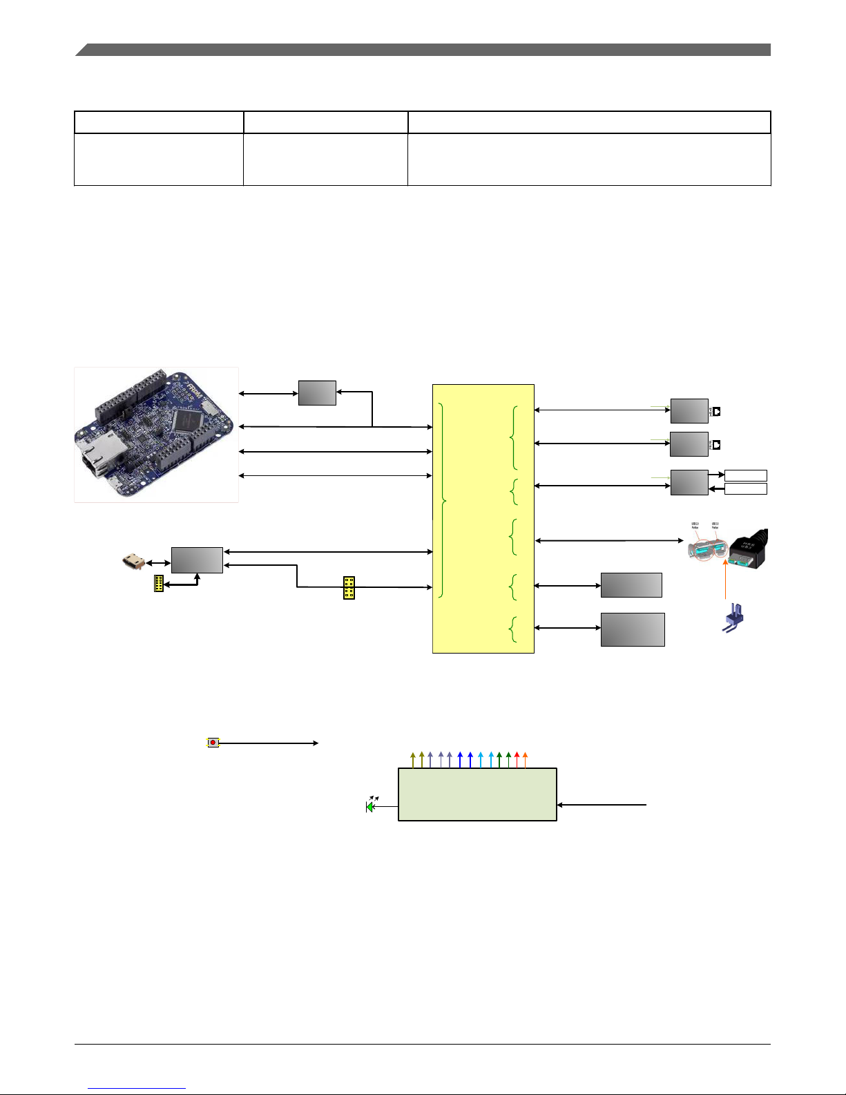
Table 1-3. FRDM-LS1012A features (continued)
FRDM-LS1012A feature Specification Description
Power supplies • 5 V input supply from USB
• 0.9 V, 1.35 V, and 1.8 V for VDD/Core, DDR, I/O, and
other board interfaces
1. For details about features of the LS1012A SoC, see QorIQ LS1012A Family Reference Manual.
1.5 FRDM-LS1012A block diagram
Figure 1-1
shows the FRDM-LS1012A block diagram.
LS1012
SVDD=0.9V,X1VDD,
AVDD_SR_PLL=1.35V
[A]
[B]
[D]
RESET
LED’s
(PG &
RESET)
USB_HVDD=3V3,
SV,SD_VDD=0.9V
SD2_REF_CLK1 & 2
2:2
OVDD=1.8V
SERDES 1
Freedom Headers
DDR3L
GVDD=1.35V
OVDD=1.8V
3 SPI Flash
I2C1
UART1
On Board Power Supply
VDD=0.9V
OVDD, TH_VD D=1.8V
MVREF=0.675V
SVDD=0.9V
USB_HVDD=3V3
EVDD=3.3
G1VDD=1.35V
XVDD =1.35V
AVDD_CGA,PLA T=1.8V
AVDD_SD1,2_P LL1,2=1.35V
USB_SVDD,SD VDD =0.9V
3V3 Board suppl y
2:3
1:3
1:2
1:2
1:2
SGMII(1G)
USB3 x2
USB2.0&USB3.0
QSPI NOR FLASH
S25FL128SAGMFI R0
OVDD=1.8V
QSPI
(Single & Dual IO)
VDD_PLAT,CGA 1,SD_REF=0.9V
DDR3L x16 SDRAM
MT 41K256M 16HA-125:E
KW24
STEREO
CODEC
SGTL5000
EMI1
SGMII PHY
REALTEK
RTL8211FS-CG
DSPI
5V from USB (Debug port)
1:2
JTAG
RESET
To LS1012A
SAI2
K20
(CMSIS DAP)
JTAG
1:2
SGMII(1G)
EMI1
SGMII PHY
REALTEK
RTL8211FS-CG
MMDC
RGMII/SAI
QSPI
USB3 PHY
AUD OUT
AUD IN
GPIO2[3:2] & GPIO1[15:19]
SPI to UART
Bridge
SC16IS740IPW
CS0
CS1
Debug uAB Port
USB3.0 PWRIN
2x1 HDR
VBUS
I2C1
Figure 1-1. FRDM-LS1012A block diagram
1.6
FRDM-LS1012A top view
The following figure shows the top view of the FRDM-LS1012A.
FRDM-LS1012A block diagram
QorIQ FRDM-LS1012A Board Reference Manual, Rev. 3, 12/2016
8 NXP Semiconductors
Page 9

Audio in
port (J13)
Audio out
port (J8)
USB 3.0
Type AB (J5)
Arduino
connectors
(J1, J2, J3, J4)
ARM JTAG
header (J9)
Header for
USB power (J12)
K20 JTAG
header (J10)
Reset switch (SW1)
USB 2.0 debug/UART
connector (J11)
SGMII PHY2
(J7), ETH2
SGMII PHY1
(J6), ETH1
SDA_LED (D1)
USB VBUS
LED (D2)
PORST LED (D3)
Figure 1-2. FRDM-LS1012A top view
Chapter 1 Overview
QorIQ FRDM-LS1012A Board Reference Manual, Rev. 3, 12/2016
NXP Semiconductors 9
Page 10

FRDM-LS1012A top view
QorIQ FRDM-LS1012A Board Reference Manual, Rev. 3, 12/2016
10 NXP Semiconductors
Page 11

Chapter 2
LS1012AFRDM Functional Description
2.1 Processor
The FRDM-LS1012A includes the QorIQ LS1012A processor that features an advanced
64-bit ARM® Cortex®-A53 processor core with ECC-protected L1 and L2 cache
memories along with datapath acceleration and network, peripheral interfaces required
for networking, wireless infrastructure, and general purpose embedded applications.
NOTE
For details about features of the LS1012A processor, see QorIQ
LS1012A Family Reference Manual.
2.2
Power supplies
The FRDM-LS1012A power supplies (PS) provide all the voltages necessary for the
correct operation of the LS1012A processor, DDR3L, QSPI memory, and other onboard
peripherals.
The following figure shows the FRDM-LS1012A power supplies.
QorIQ FRDM-LS1012A Board Reference Manual, Rev. 3, 12/2016
NXP Semiconductors 11
Page 12

LS1012
XVDD
VDD=0.9V
OVDD
G1VDD=1.35V
XVDD=1.35
SVDD=0.9V
AVDD_PLAT, XOSC_OVDD
LPF
LPF
AVDD_SD1_PLL1
LPF
LPF
USB_SDVDD
LPF
USB_HVDD
LPF
DDR
CORE
SERDES
GEN I/O
USB
1V8
LPF
USB_SVDD
0.9V/1V
USB_xVDD
AVDD_SD1_PLL2
EVDD
LPF
LPF
Passive Low Pass filters
BLM18PG121SH1
47uF
4.7nF
10uF
47uF
4.7nF
4.7uF
0.33OHm
LPF
10uF
1uF
5OHm
LPF
BLM18PG121SH1
2.2uF
0.22
LPF
1.5uF
NFM41PC155B1H3L
x2
4.7nF
22uF
0.22
LEGEND:
Switchable
Regulator
LDO Regulator
Power Switch
VDD
GVDD
VREFCA
PMIC_EN
VR5100
TA_PROG_SFP
1.89V/GND
To DDR3L
SVDD
VREF
0.9V/1V@6A
VDD
with PM Bus
Control
PMIC
SW2 (1.25A max)
GVDD=1.8V
SW1 (3.5A max)
VDD_Core =0.9V
SW3 (1.5A max)
VDD_Core =1.35V
LDO2 (0.250 max)
Unused(1.55V)
LDO1 (0.1A max)
0V/1.89V
LDO4 (0.350A)
V33 (0.35A max)
LDO3 (0.1A) 1.8V
3.3V@9A
SEPIC
USB1 3.0
PORESET_B
5V
MAX8586
USB1_DRVVBUS
LPF
AVDD_CGA1
V18 (0.1A) 1.8V
VLDOIN1/2/34;PVIN1/2/3
PVIN18, VIN, VCCI2C
REFOUT (10mA)
GVDD/2
Power OR
(FET Based w/ priority)
VBST
Unused
VSNVS
Unused
TH_VDD
DC-DC
Regulator
MC34713
To QSPI and SGTL5000
To ETH PHYs
USB CMSIS
DAP
VBUS
USB3
PWRIN
5V
Figure 2-1. FRDM-LS1012A power supplies
2.2.1
Primary power supply
The FRDM-LS1012A is powered through the CMSIS USB port (USB 2.0 Type MicroAB).
The total power required from USB port depends on devices used by an application.
Refer to the following table for an estimated power required by each of the board
interfaces.
Power supplies
QorIQ FRDM-LS1012A Board Reference Manual, Rev. 3, 12/2016
12 NXP Semiconductors
Page 13

1
Description
1 LS1012A
2 RTL8211FS(I) SGMII
3 SGTL5000
4 DDR3L (Worst case current IDD4R)
5 QSPI memory
6 K22 MCU
7 Misc (5 SSO @13mA)
Total Power
Power from 5V with efficiency of
Current
SL NO
Power (W)/QTY
0.9V
0.42
0.00867
0.297
0.045
0.0627
0.117
80%
2.37037
2.9629625
0.5925925
Watt
A
1
0.84
0.00867
0.297
0.045
0.0627
0.117
1
1
1
1
1
1
2
1.35V
1.8V
3.3V
5V
QTY
Total Power
Figure 2-2. Power estimation
An USB 2.0 host port can provide power upto 500 mA at 5 V and an USB 3.0 compliant
port can provide a maximum of 900 mA at 5 V power. Based on the type of application
and USB host port, you need to use an A-type to micro-B type Y cable to connect the two
USB host ports with the debug micro-AB port on the FRDM-LS1012A. This will double
the current capacity from host and provide required power to the FRDM-LS1012A.
NOTE
The Power estimation list does not show the power taken by the
external devices, such as USB 3.0 device, Ardiuno cards.
2.2.2
FRDM-LS1012A power supply delivery system
The following table lists the different power supply components used to generate the
various FRDM-LS1012A power supply rails.
Table 2-1. FRDM-LS1012A power supply devices
Sourc
e
volta
ge
rail
Output
voltage rail
Reference
designator
Vendor Device Description
P5V_SDAVCC_5V J11 USB2.0 MICRO-AB 5 V at 1 A power supply for onboard DC regulator
VCC_5VVCC_3V3 U7 NXP MC34713EP 3.3 V at 0.8 A power supply for:
• secondary regulator VR5100,
• onboard SGMII PHYs,
• and LS1012A supplies: EVDD and
USB_HVDD
VCC_
3V3
VCC_0V9
VCC_1V8
VCC_1V35
U8 NXP MC34VR5100A1EP Power supply for:
• LS1012A power supplies
Chapter 2 LS1012AFRDM Functional Description
QorIQ FRDM-LS1012A Board Reference Manual, Rev. 3, 12/2016
NXP Semiconductors 13
Page 14

Table 2-1. FRDM-LS1012A power supply devices
Sourc
e
volta
ge
rail
Output
voltage rail
Reference
designator
Vendor Device Description
VCC_VREF
VCC_POVDD
• DDR3L memory
• 1.8 V voltage for QSPI memory, SAI2 port,
general I/O
2.2.3 Power-ON
The FRDM-LS1012A is powered using USB power provided through a USB 2.0 Type
Micro-AB port.
The USB power provides 5 V DC voltage. The 5 V voltage powers primary power supply
regulator U7. U7 provides power supply to secondary regulator U8 and the onboard
SGMII PHYs. The secondary regulator, U8, generates power supply for peripherals, such
as QSPI flash memory and LS1012A power supplies.
Table 2-2 describes the Power-ON sequence as implemented on the FRDM-LS1012A.
Table 2-2. Power-ON process
Step Indication Specifics Description
1 5V • Power supply provided by USB2.0 Micro-AB port
• Acts as source PS for secondary regulator MC34713
2 3V3 • 3.3 V power supply for onboard SGMII PHYs and LS1012A
supplies: EVDD and USB_HVDD
• Acts as source PS for secondary regulators VR5100
3 1V8, 1V35 Power supplies provided by secondary regulator VR5100
• Provides power to peripherals and LS1012A IO and PLL
supplies (AVDD_PLAT, AVDD_CGA1, TH_VDD,
AVDD_SD1_PLL1, AVDD_SD1_PLL2, OVDD, XOSC_OVDD,
USB_SVDD, USB_SDVDD, G1VDD, VREF, SVDD, and XVDD)
4 0V9 • LS1012A core supplies: VDD
5 Red LED (D3) • Reset LED is deasserted.
2.2.4 Voltage regulation
Power supplies
QorIQ FRDM-LS1012A Board Reference Manual, Rev. 3, 12/2016
14 NXP Semiconductors
Page 15

The following table explains the FRDM-LS1012A voltage regulation.
Table 2-3. FRDM-LS1012A Voltage Regulation
Power Voltage Device Description
Core, VDD 0.9 V (3.5
A max)
VR5100 SW1 Powers the LS1012A SoC Core voltage
G1VDD 1.35 V (1.5
A max)
VR5100 SW3 Powers the LS1012A SoC DDR circuitry
VCC_VREF 0.675 V VR5100 VREF LDO
XVDD 1.35 V VR5100 SW3 Powers the LS1012A SoC SerDes I/O circuitry
AVDD_SD1_PLL1
AVDD_SD1_PLL2
SVDD 0.9 V VR5100 SW1
TH_VDD 1.8 V (1.25
A max)
VR5100 SW2 Thermal monitor unit supply voltage
AVDD_CGA1
AVDD_PLAT
Core, Platform, DDR, and SerDes PLL's supply voltages
XOSC_VDD OVDD supply for LS1012A crystal oscillator
OVDD General I/O voltage
USB_SVDD
USB_SDVDD
0.9 V VR5100 SW1 Powers the LS1012A SoC USB circuitry
USB_HVDD 3.3 V MC34713
EVDD 3.3 V MC34713
VCC_POVDD 1.8 V VR5100 LDO1 Powers the LS1012A SFP fuse programming voltage
2.3 Reset and configuration signals
The reset sequence can be triggered from various sources.
Chapter 2 LS1012AFRDM Functional Description
QorIQ FRDM-LS1012A Board Reference Manual, Rev. 3, 12/2016
NXP Semiconductors 15
Page 16

DUT_TCK
DUT_TMS
DUT_TDI
PORESET_B
DUT_TRST
DUT_TDO
JTAG
(CoreSight 10)
DUT_TJTAG_EN
DUT_PORESET
SDA_TCK
SDA_TMS
SDA_TDI
SDA_TRST
SDA_TDO
JTAG
JTAG
(CoreSight 10)
1V8
GPIO
Delay
SDHC1_CD_B/
PWR_OK
UART1
JTAG
UART
POWER_OK
Ethernet
SGMII PHYs
VSEL/
GPIO_1[23]
Voltage
Translator
1.8V
3.3V
K20
Figure 2-3. FRDM-LS1012A reset architecture
Table 2-4 summarizes the reset activity.
Table 2-4. Reset activity
Reset Source Reset Reason Actions taken
Power ON Initialization after a
power cycle.
All the onboard devices are reset after a power cycle. PLL
and clock circuitry initialize to the default configuration.
SW1 Reset switch Resets LS1012A and other board peripherals. Enables the
BOOTLOADER mode on the K20 CMSISDAP.
Debugger reset (J9 and K20) Reset from JTAG
debugger
No power cycle. All devices are reset.
RESET_REQ_B Reset request from
LS1012A
All devices are reset. No power cycle.
The reset is asserted for about 240 ms after all power supplies are stable. This is to meet
the LS1012A 100 ms reset specification. Power failure after system operation also asserts
the reset to all the devices on the board. The FRDM-LS1012A supports options to change
the PORCFG through the resistor mount option. Mount the resistors to drive the
corresponding PORCFG as low in Table 2-5.
Table 2-5. Configuration signals
Configuration signal Nets sampled Components on board
Default state
CFG_RCW_SRC1 CLK_OUT R50 DNP
Reset and configuration signals
QorIQ FRDM-LS1012A Board Reference Manual, Rev. 3, 12/2016
16 NXP Semiconductors
Page 17

2.4 Clocks
The architecture of the FRDM-LS1012A clocks is shown in the following figure.
LS1012
EXTAL
ETH SGMII
PHY
RTL8211FS-CG
ETH SGMII
PHY
RTL8211FS-CG
8 MHz
Crystal
K20
Audio
SGTL5000
25MHz
25MHz
SPI to UART
Bridge
SC16IS740IPW
XO
24MHz
24MHz
1:4
CLK
BUFER
25MHz
XO
25MHz
Figure 2-4. Clock architecture
The following table summarizes the FRDM-LS1012A clock distribution.
Table 2-6. FRDM-LS1012A clocks
Clock Frequency Destination Device
EXTAL (Bypass mode) 25 MHz Input clock for SoC
ETH1_REFCLK 25 MHz Reference clock for the
SGMII PHY1
Oscillator (KC2520C25.0000C1LE00) and
clock buffer, 524S:
• Additive phase jitter RMS = 50 fs
• Skew outputs = 50 ps
• Low cost clock buffer
• Input/Output clock frequency up to
200 MHz
ETH2_REFCLK 25 MHz Reference clock for the
SGMII PHY2
CODEC_SYS_MCLK 25 MHz System clock for audio
codec
8MHz XTAL for K20 8 MHz Crystal clock for K20 Crystal
BRDG_CLKIN_24MHz 24 MHz Clock for SC16IS740IPW
SPI to Dual UART bridge
Oscillator
Chapter 2 LS1012AFRDM Functional Description
QorIQ FRDM-LS1012A Board Reference Manual, Rev. 3, 12/2016
NXP Semiconductors 17
Page 18

2.5 Double data rate (DDR) memory
The FRDM-LS1012A supports One 512 MB DDR3L SDRAM memory, running at data
rates up to 1000 MT/s. The part number is Micron MT41K256M16TW-107:P.
Following are the characteristics of the LS1012A DDR3L memory controller:
• Up to 1.0 GT/s
• Supports 16-bit operation (no ECC support)
• Support for x8, x16 devices
• Supports 1 chip select, D1_MCS_B
The VR5100 VREF LDO (U8) takes 1.35 V supply and provides 0.675 V VREF supply
to the DDR3L memory.
The memory interface includes all the necessary termination and I/O power, and is routed
so as to achieve maximum performance of the memory bus.
2.6
Serializer/deserializer (SerDes)
The FRDM-LS1012A SerDes block provides two high-speed serial communication lane,
supporting SGMII PHYs. See QorIQ LS1012A Data Sheet for details about the SerDes
protocols supported on the LS1012A processor. The following table lists the components
used to support the different SerDes options.
Table 2-7. FRDM-LS1012A SerDes embedded devices
Manufacturer Part number Description Lane supported Speed
Realtek RTL8211FS-CG • SGMII 1G PHY x1 1.25 Gbit/s
Realtek RTL8211FS-CG • SGMII 1G PHY x1 1.25 Gbit/s
2.7 Ethernet controller
The LS1012A processor supports two Ethernet MACs, which connect to the onboard
PHYs using the SGMII protocols.
2.7.1
SGMII ports
Double data rate (DDR) memory
QorIQ FRDM-LS1012A Board Reference Manual, Rev. 3, 12/2016
18 NXP Semiconductors
Page 19

The onboard Ethernet PHYs, Realtek RTL8211FS (U16 and U17), are connected to the
LS1012A processor EC1 and EC2 using the SGMII protocol over SerDes lane A and
SerDes lane B.
MDIO
MDC
Ethernet Controller
LS1012
3V3
3V3
3V3_RST_B
SGMII
MDI_0_P/N
MDI_1_P/N
MDI_3_P/N
MDI_2_P/N
PMEB
INTB
PHYRSTB
DVDD_RG
DVDD33
4.7K
PHY
SUPPORT
MODE: SGMII
RJ-45
1Gbps
100Mbps
3V3
4.7K
1V
REG_OUT
AVDD10
DVDD10
AVDD33
0 ohm
#1
REALTEK RTL8211FS-CG
48-PIN QFN
Notes and Assumptions:
- MAC connected to Serdes lane B is the same MAC connected to the RGMII interface.
so RGMII and SGMII ( lane B) can not be use at a time.
- If the Serdes is configured for 2 SGMII interfaces, then the RGMII interface is unused
(tristated unless the pinmuxing control register is configured for functionality other than
EC1 RGMII).
SERDES
Lane A
TX_P/N
RX_P/N
HSIP/N
HSOP/N
EM1_MDC
EM1_MDIO
X
Transfo rmer
OVDD
1.8V
Voltage
Translator
1.8V
3.3V
VSEL/
GPIO_1[13]
Figure 2-5. SGMII PHY1
Chapter 2 LS1012AFRDM Functional Description
QorIQ FRDM-LS1012A Board Reference Manual, Rev. 3, 12/2016
NXP Semiconductors 19
Page 20

MDIO
MDC
Ethernet Controller
LS1012
3V3
3V3
PHY_RST1
SGMII
MDI_0_P/N
MDI_1_P/N
MDI_3_P/N
MDI_2_P/N
PMEB
INTB
PHYRSTB
DVDD_RG
DVDD33
4.7K
PHY
SUPPORT
MODE: SGMII
RJ-45
1Gbps
100Mbps
3V3
4.7K
1V
REG_OUT
AVDD10
DVDD10
AVDD33
0 ohm
#1
REALTEK RTL8211FS-CG
48-PIN QFN
Notes and Assumptions:
- MAC connected to Serdes lane B is the same MAC connected to the RGMII interface.
so RGMII and SGMII ( lane B) can not be use at a time.
- If the Serdes is configured for 2 SGMII interfaces, then the RGMII interface is unused
(tristated unless the pinmuxing control register is configured for functionality other than
EC1 RGMII).
SERDES
Lane B
TX_P/N
RX_P/N
HSIP/N
HSOP/N
EM1_MDC
EM1_MDIO
X
Transfo rmer
Voltage
Translator
1.8V
3.3V
VSEL/
GPIO_1[13]
Figure 2-6. SGMII PHY2
Table 2-8. Hardware bootstrap settings for Ethernet PHYs
Setting Description
PHY_AD[2:0] = 001 PHY Addr = 0b00010 (for SGMII PHY1)
PHY Addr = 0b00001 (for SGMII PHY2)
CFG_LDO[1:0] = 10 External power voltage selections for IO pads (1.8 V)
CFG_MODE[2:0] = 011 UTP > SGMII
Table continues on the next page...
Ethernet controller
QorIQ FRDM-LS1012A Board Reference Manual, Rev. 3, 12/2016
20 NXP Semiconductors
Page 21

Table 2-8. Hardware bootstrap settings for Ethernet PHYs (continued)
Setting Description
TXDLY = 1 RGMII TXC clock skew = 2.0 ns (through Register setting #17.8)
RXDLY = 1 RGMII TXC clock skew = 2.0 ns
2.8 Audio interface
The FRDM-LS1012A board supports the audio interface using the SGTL5000 codec.
This codec connects with LS1012A on the SAI2 interface.
SAI2 supports full duplex audio and takes bit clock (TX and RX BCLK) and frame clock
(TX and RX SYNC) as input from SGTL5000. The SGTL5000 generates these clocks
based on a 25 MHz MCLK, which is fed from the CLKOUT of LS1012A. The
SGTL5000 control interface is I2C-based and can be accessed at the 0x0A address.
2.9
USB interface
The FRDM-LS1012A board supports:
• one SuperSpeed USB 2.0/3.0 port - configured as On-The-Go (OTG) with a MicroAB connector. Based on the OTG configuration, the PHY can either operate in TypeA or Type-B mode
• a 2-pin header (J12) to provide 5 V at 1 A power supply to the USB 2.0/3.0 port
The following figure shows the USB 2.0/3.0 PHY architecture on the FRDM-LS1012A.
Chapter 2 LS1012AFRDM Functional Description
QorIQ FRDM-LS1012A Board Reference Manual, Rev. 3, 12/2016
NXP Semiconductors 21
Page 22

LS1012
5V
USB3 Micro - AB
USB1_DRVVBUS
USB1
USB1_PWRFAULT
USB1_VBUS
90 Ohm Diff. Impedance
USB1_DP,DM
USB1_TXP,TXM
USB1_RESREF
USB1_RXP,RXM
USB1_ID
HVDD=3V3
OVDD=1V8
MAX8586
<=1.5A
USB1_5V
USB1_5V
2x1 Header
Figure 2-7. USB 2.0/3.0 PHY architecture
NOTE
Connect the micro-B to type-A USB cable to the onboard USB
2.0 debug port, J11, to turn on the board.
2.10
I2C ports
The FRDM-LS1012A support one I2C bus:
• The LS1012A I2C1 is attached to the local devices on the FRDM-LS1012A.
• The level shifter device (NTSX2102GU8H) is used on the FRDM-LS1012A I2C1
bus, to convert the LS1012A 1.8 V to 3.3 V signals for the I2C devices, on Arduino/
Freedom expansion connectors.
• The I2C1 bus has one possible master - LS1012A processor.
2.10.1
I2C devices and addresses
I2C ports
QorIQ FRDM-LS1012A Board Reference Manual, Rev. 3, 12/2016
22 NXP Semiconductors
Page 23

The LS1012A I2C1 interface operates at 1.8 V OVDD power supply. Table 2-9
summarizes the I2C bus device addresses.
NOTE
7-bit addresses do not include the R/W bit as an address
member, though some datasheets might do so. For consistency,
all I2C addresses are 7 bits of addresses only.
Table 2-9. I2C bus device map
I2C bus I2C address Device Notes
I2C1 0x0a SAI audio codec • SAI 2 port with full duplex support
n/a Arduino Shield • Provides support for Ardiuno and
Freedom shield expansion
0X08 MC34VR5100A1EP • Power supply for:
• LS1012A power supplies
• DDR3L memory
• 1.8 V voltage for QSPI memory,
SAI2 port, general I/O
2.11 QSPI interface
The FRDM-LS1012A supports QSPI as the primary system boot source. The FRDMLS1012A supports onboard Spansion S25FS512SAGNFI011 quad-SPI serial flash
memory with 64 MB space.
LS1012A supports only one QSPI controller with 1 chip select, PROC_QSPI_CS_B. The
board doesn't support the quad mode, only single and dual bit modes are supported.
2.12
SPI interface
The FRDM-LS1012A SPI features are as follows:
• SPI bus interface is connected to a high performance UART bridge, SC16IS740IPW.
The UART interface connects to devices on Arduino/Freedom expansion connectors.
• SPI bus interface can also connect to the Ardiuno shield, J2, via level translators.
The following table describes the SPI devices used on the FRDM-LS1012A board.
Chapter 2 LS1012AFRDM Functional Description
QorIQ FRDM-LS1012A Board Reference Manual, Rev. 3, 12/2016
NXP Semiconductors 23
Page 24

Table 2-10. SPI master mode onboard devices
Device Voltage range SPI CS
SC16IS740IPW 3.3 V SPI_CS0
Ardiuno Shield J2 connector 3.3 V SPI_CS1
2.13 Ardiuno
The FRDM-LS1012A board supports a Freedom board or an Ardiuno shield on
connectors J1 to J4 to provide broad range of board expansion options.
Arduino supports following interfaces:
• SPI connectivity from the LS1012A on CS1.
• UART connectivity through the LS1012A SPI to the UART bridge.
• I2C connectivity from the LS1012A.
2.14
JTAG port
The FRDM-LS1012A consists of the LS1012A SoC and the K20 microcontroller, each of
which have dedicated debug connectors.
• J9 and J10 can be used by external debuggers, such as CWTAP, DSTREAM to
debug LS1012A and K20 respectively
• Apart from the JTAG connectors, the K20 MCU can be used as a CMSIS DAP on
the FRDM-LS1012A. The CMSIS DAP provides low speed debug functionality for
LS1012A.
2.14.1
CMSIS-DAP
This section describes the MBED circuit on the LS1012AFRDM. MBED is an open
standard serial and debug adapter. It bridges serial and debug communications between a
USB host and an embedded target processor, as shown in the figure below.
Ardiuno
QorIQ FRDM-LS1012A Board Reference Manual, Rev. 3, 12/2016
24 NXP Semiconductors
Page 25

LS1012A
nRESET
K20 MCU
MSD
bootloader
CMSIS-DAP
application
UART0 Tx/Rx
JTAG signals
GPIO
UART Tx/Rx
GPIO
OpenSDA CMSIS-DAP
USB host
USB
Figure 2-8. CMSIS-DAP
CMSIS-DAP is managed by a Kinetis K20 MCU built on the ARM Cortex-M4 core. The
Kinetis K20 includes an integrated USB controller (USB 2.0 Micro-AB) port that can
operate at clock rates of up to 120 MHz. The CMSIS-DAP circuit includes a status LED.
In addition, signal connections are available to implement a UART serial channel.
CMSIS-DAP features a mass storage device (MSD) bootloader, which provides a quick
and easy mechanism for loading different CMSIS-DAP applications, such as flash
programmers, run control debug interfaces, serial-to-USB converters, and so on.
2.15
GPIO pins
LS1012A has no dedicated GPIO pins; instead the FRDM-LS1012A provides GPIOs
through Ardiuno shield.
Table 2-11. FRDM-LS1012A - GPIO mapping
Primary function GPIO function Connections on FRDM board
SDHC1_CMD DUT_GPIO_1[15] Connects LS1012A to Arduino
SDHC1_DAT0 DUT_GPIO_1[16] Connects LS1012A to Arduino
SDHC1_DAT1 DUT_GPIO_1[17] Connects LS1012A to Arduino
SDHC1_DAT2 DUT_GPIO_1[18] Connects LS1012A to Arduino
SDHC1_DAT3 DUT_GPIO_1[19] Connects LS1012A to Arduino
SDHC1_CLK DUT_GPIO_1[20] Connects LS1012A to Arduino
EC1_TXD3 DUT_GPIO_2[2] Connects LS1012A to Arduino through 1.8 V to 3.3 V translators
EC1_TXD2 DUT_GPIO_2[3] Connects LS1012A to Arduino through 1.8 V to 3.3 V translators
Chapter 2 LS1012AFRDM Functional Description
QorIQ FRDM-LS1012A Board Reference Manual, Rev. 3, 12/2016
NXP Semiconductors 25
Page 26

2.16 Temperature
LS1012A has an on-die TMU module that can be used for temperature measurements.
LS1012A also has a thermal diode on the die, which allows direct temperature
measurement. The internal temperature monitor in LS1012A is used for reading the die
temperature, and trigger software interrupts upon thermal over-temperature conditions.
These temperature warnings and alarm signals can be used by software running on
LS1012A to reduce the power dissipation and protect DUT from over-temperature
failure.
2.17
Power-monitoring LEDs
The board includes LEDs, for power or reset monitoring, which inform the user about the
status of different power rails, resets, and board faults. The FRDM-LS1012A LEDs are
listed in the following table.
Table 2-12. FRDM-LS1012A LEDs
LED legend Description (when LED is ON) Reference
designator
LED color
USB VBUS ON Indicates that USB 5 V power is available on the connector D2 Green
SDA_LED Indicates SDA (K20) is active D1 Green
PORST DUT is in reset (PORESET is asserted) D3 Red
2.18 Revision control
The GPIO2[14], GPIO2[12], and GPIO1[11] are used to determine the board revision of
FRDM-LS1012A. The following table explains the board revisions.
Table 2-13. Revision control
{GPIO2[14], GPIO2 [12], GPIO2[11] } VERSION
0x0 Rev B
0x1 Rev C
Temperature
QorIQ FRDM-LS1012A Board Reference Manual, Rev. 3, 12/2016
26 NXP Semiconductors
Page 27

Appendix A
FRDM-LS1012A board drawings
This section explains:
• FRDM-LS1012A top-side view
• FRDM-LS1012A bottom-side view
A.1
FRDM-LS1012A top-side view
NOTE
For a clear view of the board top-side view, please zoom-in on
the Figure.
Figure A-1. FRDM-LS1012A top-side view
QorIQ FRDM-LS1012A Board Reference Manual, Rev. 3, 12/2016
NXP Semiconductors 27
Page 28

A.2 FRDM-LS1012A bottom-side view
NOTE
For a clear view of the board bottom-side view, please zoom-in
on the Figure.
Figure A-2. FRDM-LS1012A bottom-side view
FRDM-LS1012A bottom-side view
QorIQ FRDM-LS1012A Board Reference Manual, Rev. 3, 12/2016
28 NXP Semiconductors
Page 29

Appendix B
Revision history
This sections summarizes revisions to this document.
Table B-1. Revision history
Revision Date Section Description
0 06/2016 Initial public release.
1 08/2016 Incorporated branding changes
2 08/2016 FRDM-LS1012A features
Double data rate (DDR) memory
QSPI interface
Updated DDR and QSPI memory sizes to bytes instead
of bits
3 12/2016 Reset and configuration signals Updated Table 2-5 table to remove components: R35
and R49
FRDM-LS1012A top view Updated top view for Rev c board
FRDM-LS1012A block diagram Updated FRDM-LS1012A block diagram for the Rev C
board
Voltage regulation Updated Table 2-3 to add "VCC_POVDD"
Clocks In Table 2-6, updated:
• "25MHz (XTAL)" to "EXTAL (Bypass mode)"
• "Clock buffer, 524S" to "Oscillator
(KC2520C25.0000C1LE00) and Clock buffer,
524S"
I2C ports Added device "MC34VR5100A1EP"
Revision control Added details for GPIOs used to determine board
revision
FRDM-LS1012A board drawings Updated top-side and bottom-side assembly drawings
GPIO pins Updated Table 2-11 to:
• Remove "SDHC1_VSEL" row
• Remove translators details from SDHC1 rows
QorIQ FRDM-LS1012A Board Reference Manual, Rev. 3, 12/2016
NXP Semiconductors 29
Page 30

QorIQ FRDM-LS1012A Board Reference Manual, Rev. 3, 12/2016
30 NXP Semiconductors
Page 31

How to Reach Us:
Home Page:
nxp.com
Web Support:
nxp.com/support
Information in this document is provided solely to enable system and software
implementers to use NXP products. There are no express or implied copyright
licenses granted hereunder to design or fabricate any integrated circuits based
on the information in this document. NXP reserves the right to make changes
without further notice to any products herein.
NXP makes no warranty, representation, or guarantee regarding the suitability of
its products for any particular purpose, nor does NXP assume any liability arising
out of the application or use of any product or circuit, and specifically disclaims
any and all liability, including without limitation consequential or incidental
damages. “Typical” parameters that may be provided in NXP data sheets and/or
specifications can and do vary in different applications, and actual performance
may vary over time. All operating parameters, including “ typicals ,” must be
validated for each customer application by customer's technical experts. NXP
does not convey any license under its patent rights nor the rights of others. NXP
sells products pursuant to standard terms and conditions of sale, which can be
found at the following address: nxp.com/SalesTermsandConditions .
NXP, the NXP logo, Freescale, the Freescale logo, and QorIQ are trademarks of
are trademarks of NXP B.V. All other product or service names are the property
of their respective owners. ARM, Cortex are registered trademarks of ARM
Limited (or its subsidiaries) in the EU and/or elsewhere. All rights reserved.
© 2015-2016 NXP B.V.
.
Document Number FRDM-LS1012ARM
Revision 3, 12/2016
 Loading...