

Page 1

Development Kit for Wearable Devices
Featuring the QN9080 BLE SoC
Quick Start Guide
QN9080 Development Kit
Page 2
2
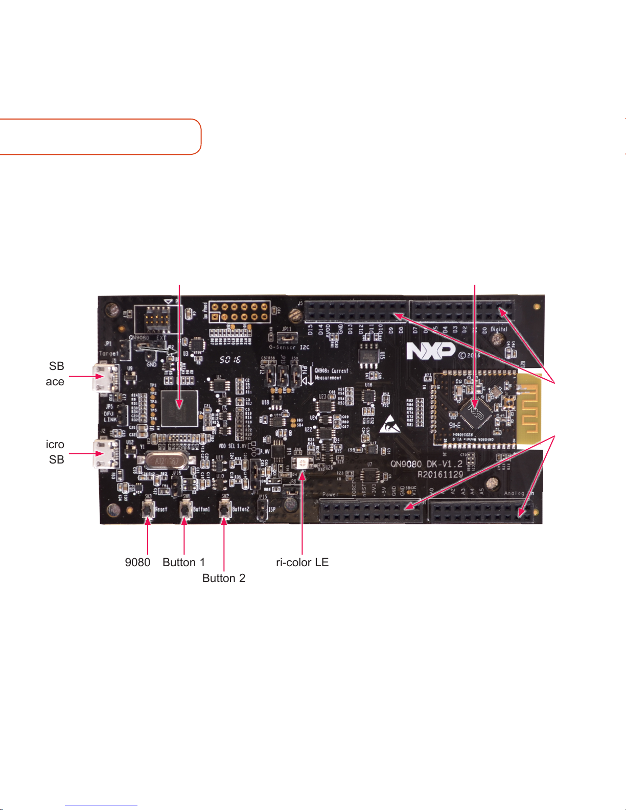
Figure 1: Front side of QN9080 Development Kit
Tri-color LED
Button 2
Button 1QN9080
RESET
Micro
USB
USB
Interface
Arduino®
Headers
Debugger QN9080 SoC
GET TO KNOW THE QN9080 DEVELOPMENT KIT
Page 3

3
www.nxp.com
STEP-BY-STEP INSTRUCTIONS
2
Power On
& Advertise
Connect the micro-USB cable into the
bottom USB port (J2) to power the board.
Press button 1 to start advertising.
3
Open
App
Open the Kinetis BLE Toolbox
app and click on Proximity.
4
Choose Your
Device
5
Select
Alerts
Click Immediate Alert -> High to make
the board LED blink green two times per
second. Click Immediate Alert -> Middle
to make it blink once per second.
1
Download
Software
Download Kinetis® BLE Toolbox
to your smartphone.
Google Play™ store:
https://goo.gl/yCl4j7
Apple® App Store:
https://goo.gl/TXunnk
Page 4

www.nxp.com/QN9080
NXP and the NXP logo are trademarks of NXP B.V. All other product or service names are the property of
their respective owners. © 2017 NXP B.V.
Document Number: QN9080DKQSG REV 0
Agile Number: 926-29625 REV A
SUPPORT
Visit www.nxp.com/support for a list of
phone numbers within your region.
WARRANTY
Visit www.nxp.com/warranty for
complete warranty information.
The following information is provided per Article 10.8 of the Radio Equipment Directive 2014/53/EU:
(a) Frequency bands in which the equipment operates.
(b) The maximum RF power transmitted.
EUROPEAN DECLARATION OF CONFORMITY (Simplified DoC per Article 10.9 of the Radio Equipment
Directive 2014/53/EU)
This apparatus, namely QN9080 Development Kit for wearable devices, conforms to the Radio Equipment
Directive 2014/53/EU.
The full EU Declaration of Conformity for this apparatus can be found at: nxp.com/QN9080DK
Get Started
Explore more features
and get started on your design at
www.nxp.com/qn9080/starthere.
PN RF Technology (a) Freq Ranges (EU)
(b) Max Transmitted
Power
QN9080-DK BLE 2400~2483.5 MHz +2 dBm
 Loading...