

Page 1

QN902x
User Manual of QN902x
Rev. 1.3 — 05 November 2018
User Manual
Document information
Info
Content
Keywords
User manual, MCU, Register
Abstract
This document is a user manual of QN902x SoC.
Page 2

NXP Semiconductors
QN902x
User Manual of QN902x
UM10996
All information provided in this document is subject to legal disclaimers.
© NXP Semiconductors N.V. 2018. All rights reserved.
User Manual
Rev 1.3 — 05 November 2018
2 of 128
Contact information
For more information, please visit: http://www.nxp.com
Revision history
Rev
Date
Description
1.0
20150715
First version.
1.1
20160408
Updated some register description.
1.2
20180423
Updated Section 2.3, “Memory Organization”.
1.3
20181105
Added description on fast boot function. Removed description on QN902x temperature sensor.
Page 3
NXP Semiconductors
QN902x
User Manual of QN902x
UM10996
All information provided in this document is subject to legal disclaimers.
© NXP Semiconductors N.V. 2018. All rights reserved.
User Manual
Rev 1.3 — 05 November 2018
3 of 128
1. Introduction
This document is a user manual for the QN902x SoC. It describes in detail the principle
and register information of the main components of the QN902x. The audience of this
document are technical and experienced engineers in design and development area
based on SoC.
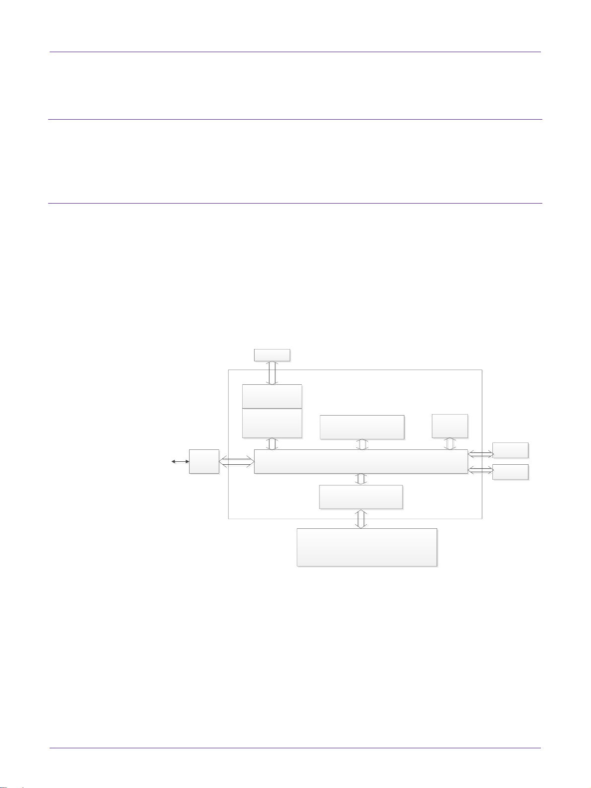
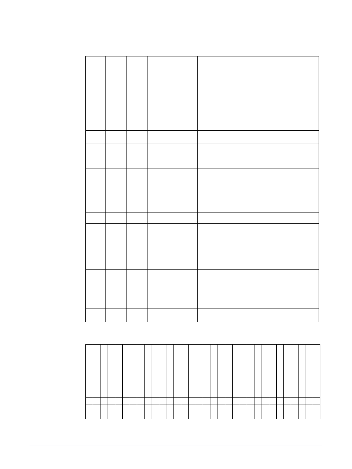
2. MCU Subsystem
The MCU system includes:
32-bit ARM Cortex-M0 MCU
AHB-Lite bus system
64kB system memory
Clock, reset and power management units
Two-wire debug interface (SWD)
24-bit system tick timer
Block diagram is shown as below figure.
ARM
CORTEX-M0
AHB-LITE BUS
DEBUG
INTERFACE
SWD
System Memory
64kB
ROM
AHB to APB BRIDGE
GPIO
ADC
AES-128
Periperals
MCU
Figure 1 QN902x MCU subsystem block diagram
2.1 MCU
The CPU core is a 32-bit ARM Cortex-M0 core, which offers significant benefits to
application development including:
Simple and easy-to-use programmer’s model
Highly efficient ultra-low power operation
Excellent code density
Page 4

NXP Semiconductors
QN902x
User Manual of QN902x
UM10996
All information provided in this document is subject to legal disclaimers.
© NXP Semiconductors N.V. 2018. All rights reserved.
User Manual
Rev 1.3 — 05 November 2018
4 of 128
Deterministic, high-performance interrupt handling of 32 external interrupt
inputs
The processor has been extensively optimized for low power, and delivers exceptional
power efficiency through its efficient instruction set, providing high-end processing
hardware including a single-cycle multiplier. The exceptional low power, small gate count
and code footprint of the processor makes it ideal for ultra-low power MCU and mixed
signal applications, delivering 32-bit performance and efficiency.
2.1.1 Nested Vectored Interrupt Controller (NVIC)
NVIC of QN902x supports 32 external interrupt inputs, each with four levels of priority. It
also supports both, level-sensitive and edge-sensitive interrupt lines.
External interrupt signals are connected to the NVIC, and the NVIC prioritizes the
interrupts. Software can set the priority of each interrupt. The NVIC and the Cortex-M0
processor core are closely coupled, providing low latency interrupt processing and
efficient processing of late arriving interrupts.
The Wake-up Interrupt Controller (WIC) supports ultra-low power sleep mode. This
enables the processor and NVIC to be put into a very low-power sleep mode leaving the
WIC to identify and prioritize the interrupts. The processor fully implements the WaitFor-Interrupt (WFI), Wait For Event (WFE) and the send Event (SEV) instructions. In
addition, the processor also supports the use of SLEEPONEXIT, which causes the
processor core to enter sleep mode when it returns from an exception handler in Thread
mode.
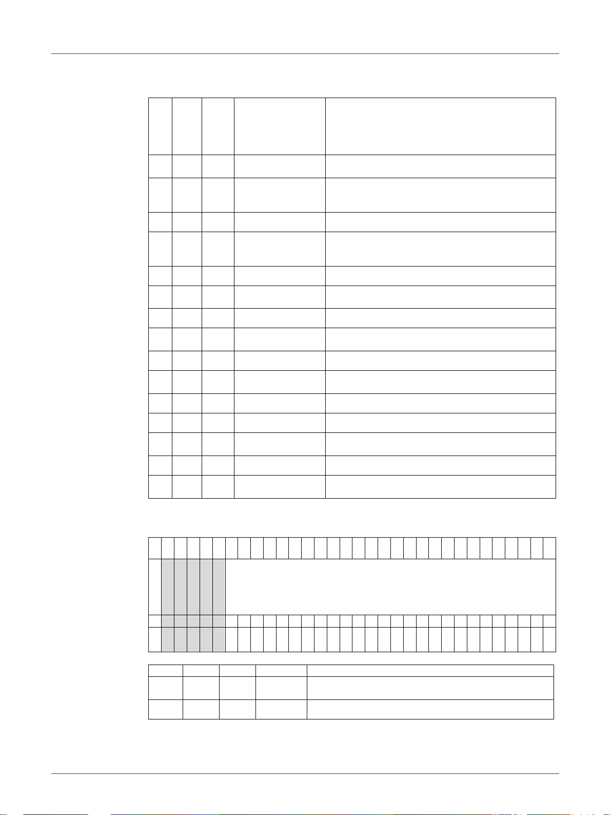
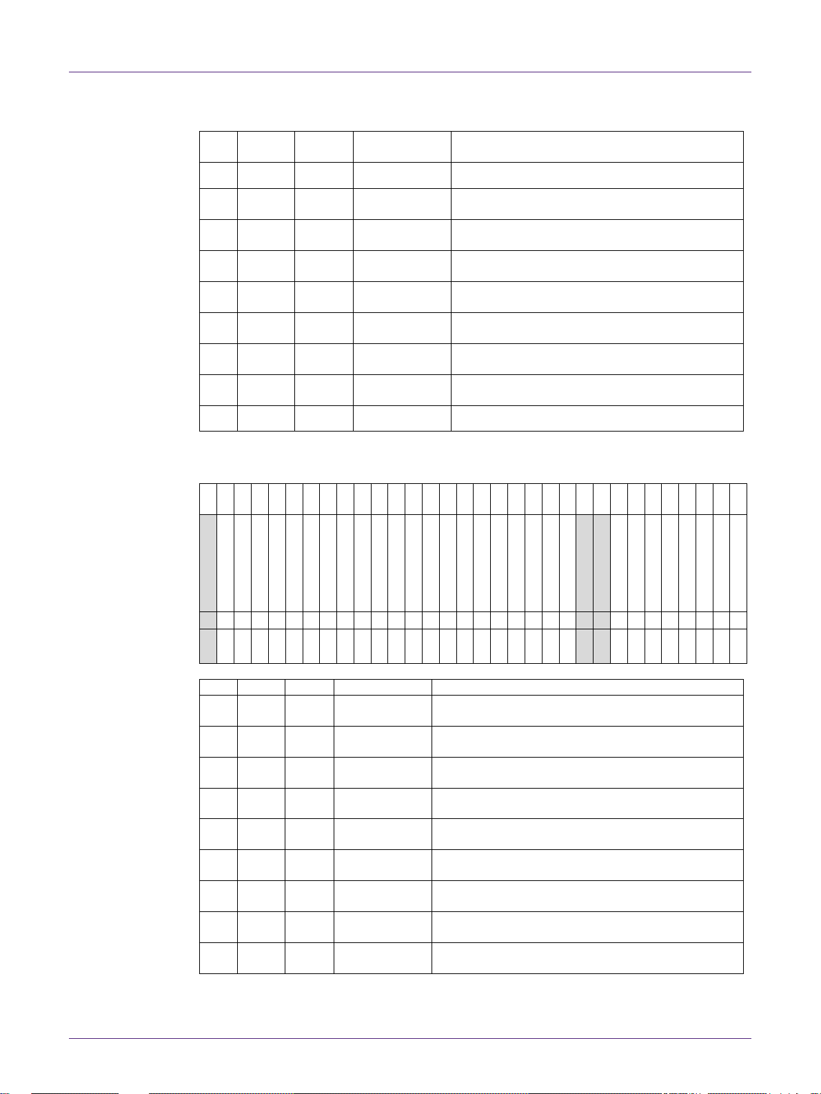
Table 1 Interrupt Sources
IRQ#
Source
IRQ#
Source
0
GPIO
16
SPI1_TX
1
ACMP0
17
SPI1_RX
2
ACMP1
18
I2C 3 BLE_Interrupt
19
TIMER0
4
RTC_Capture
20
TIMER1
5
OSC_EN
21
TIMER2
6
RTC Timeout
22
TIMER3
7
ADC
23
WatchDog
8
DMA
24
PWM0
9
ANT_RX
25
PWM1
10
UART0_TX
26
Calibration
11
UART0_RX
27
Proprietary_RX
12
SPI0_TX
28
Proprietary_TX
13
SPI0_RX
29
BLE_RX
14
UART1_TX
30
BLE_TX
15
UART1_RX
31
BLE_FRQ_JUMP
Page 5

NXP Semiconductors
QN902x
User Manual of QN902x
UM10996
All information provided in this document is subject to legal disclaimers.
© NXP Semiconductors N.V. 2018. All rights reserved.
User Manual
Rev 1.3 — 05 November 2018
5 of 128
2.1.2 Serial Wire Debug (SWD) interface
The QN902X supports Serial Wire Debug Port (SW-DP) interface. The debug pins (SWCLK,
SWDIO) share the pins with normal function pins, with debug being the default state.
In addition, it supports 4 hardware breakpoints and 2 watchpoints. The basic debug
functionality includes processor halt, single-step, processor core register access, Reset
and HardFault Vector Catch, unlimited software breakpoints, and full system memory and
register access.
For security purpose, the debug interface cannot read locked instruction memory content.
It can only read the unlocked instruction space. The security is controlled by the user.
2.1.3 System Timer (SYSTICK)
SYSTICK provides a simple, 24-bit clear-on-wire, decrementing, wrap-on-zero counter
with a flexible control mechanism, which is intended to generate a dedicated SYSTICK
exception at a fixed time interval.
2.2 System Bus
The QN902X contains an AHB-Lite bus system to allow bus masters to access the memory
mapped address space. A multilayer AHB bus matrix connects the 2 master bus interfaces
to the AHB slaves. The bus matrix allows several AHB slaves to be accessed
simultaneously. The 2 AHB bus master are: MCU and DMA.
An AHB-to-APB bridge is connected to the AHB bus matrix, to access the low speed
peripherals. The APB can run on lower clock than AHB for low power consumption.
2.3 Memory Organization
The memory architecture is a ROM + Flash + RAM architecture, with the ROM storing the
BLE stack, the Flash being used for application program and data storage. During the boot,
the program is loaded from the Flash to the RAM. This allows execution with system clock
up to 32MHz and reduction of the active current consumption compared to the execution
from the Flash.
The QN902x supports 96 kB of ROM and 128 kB of flash (QN9020/1). The ROM space is
not accessible to users. The system RAM memory is 64kB in size for application program
and data, which consists of 8 blocks, addresses for them are allocated as below.
- Memory 0 : 10000000 ~ 10001fff
- Memory 1 : 10002000 ~ 10003fff
- Memory 2 : 10004000 ~ 10005fff
- Memory 3 : 10006000 ~ 10007fff
- Memory 4 : 10008000 ~ 10009fff
- Memory 5 : 1000a000 ~ 1000bfff
- Memory 6 : 1000c000 ~ 1000dfff
- Memory 7 : 1000e000 ~ 1000ffff
Page 6
NXP Semiconductors
QN902x
User Manual of QN902x
UM10996
All information provided in this document is subject to legal disclaimers.
© NXP Semiconductors N.V. 2018. All rights reserved.
User Manual
Rev 1.3 — 05 November 2018
6 of 128
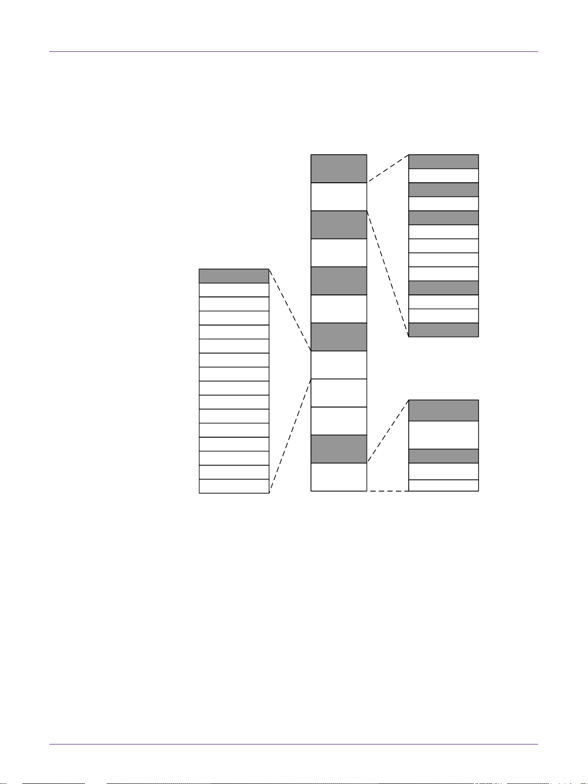
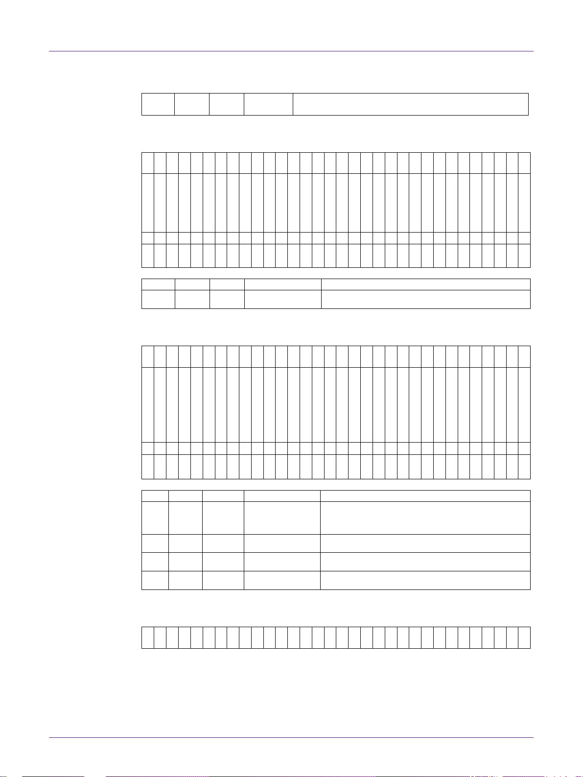
The system memory (ROM + SRAM + Flash), all registers and external devices are
allocated in the same memory map within 4GB, ranging from 0x00000000 to 0xFFFFFFFF,
which is shown in the following Figure 2. The system memory security is ensured with a
user controllable protection scheme, preventing un-authorized read out.
Code
0x00000000
0x1FFFFFFF
BLE Processor
Memory
0x2F000000
0x2FFFFFFF
Serial FLASH
0x30000000
0x3FFFFFFF
APB peripherals
0x40000000
0x400EFFFF
0x400F0000
0x4FFFFFFF
GPIO
0x50000000
0x50003FFF
0x50004000
0x50007FFF
ADC
0x50010000
0x50013FFF
0x50014000
0xDFFFFFFF
Private peripheral
0xE0000000
0xEFFFFFFF
0xF0000000
0xFFFFFFFF
ROM
(96 KB)
0x01000000
0x01018000
System SRAM
0x10000000
0x1000FFFF
System Registers
0x40000000
Watch Dog Timer
0x40001000
Timer0
0x40002000
Timer1
0x40003000
Timer2
0x40004000
Timer3
0x40005000
RTC
0x40006000
USART0
0x40007000
I2C
0x40008000
DMA
0x40009000
USART1
0x4000A000
BLE Physical DataPath
0x4000B000
PWM
0x4000C000
0xE0000000
Watchpoint unit
0xE0001000
Breakpoint unit
0xE0002000
0xE0003000
Auxiliary Control
Registers
0xE000E000
System Timer
0xE000E010
NVIC
0xE000E100
System Control Block
0xE000ED00
0xE000ED90
Debug Control Registers
0xE000EDF0
0xE000EF00
ROM Table
0xE00FF000
0xE0100000
0x20000000
0x2EFFFFFF
BootLoader
0x00000000
Calibration
Proprietary Interface
0x4000D000
0x4000E000
Figure 2 QN902X System Address Space
2.4 Reset Management Unit (RMU)
The RMU ensures correct reset operation. A correct reset sequence is needed to ensure
the safe startup. The RMU provides proper reset and startup, even in the case of error
situations such as power supply glitches or software crash.
Reset sources:
Power-on Reset (POR)
Brown-out Detection (BOD)
RESET pin
Watchdog timeout reset
Page 7

NXP Semiconductors
QN902x
User Manual of QN902x
UM10996
All information provided in this document is subject to legal disclaimers.
© NXP Semiconductors N.V. 2018. All rights reserved.
User Manual
Rev 1.3 — 05 November 2018
7 of 128
The Power-on Reset and Brown-out detectors provide power line monitoring with
exceptional low power consumption. The cause of the reset may be read by the
software from the registers.
The RST_CAUSE_SRC register indicates the reason for the last reset. The register should
be cleared after read at the startup. Otherwise the register may indicate multiple reset
causes at next startup. Note that it is possible to have multiple reset causes. For example,
an external reset and a watchdog reset may happen simultaneously. For more
information, please see RST_CAUSE_SRC (RCS) register description.
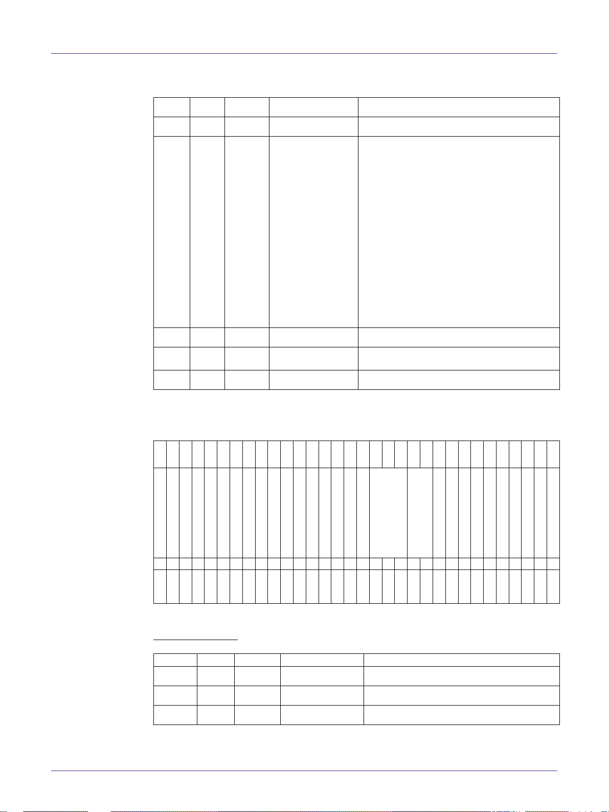
2.5 Register Description
2.5.1 Register Map
The MCU subsystem register base address is 0x40000000.
Table 2 Register Map
Offset
Name
Description
000h
CRSS
Enable clock gating and set block reset
004h
CRSC
Disable clock gating and clear block reset
008h
CMDCR
Set clock switch and clock divider
00Ch
STCR
Set systick timer STCALIB and STCLKEN
014h
SOCR
Reserved. Don’t change
020h
PMCR0
PIN Mux control 0
024h
PMCR1
PIN Mux control 1
028h
PMCR2
PIN Mux control 2
02Ch
PDCR
PAD Driver control
030h
PPCR0
PAD Pull-up and Pull-down control 0
034h
PPCR1
PAD Pull-up and Pull-down control 1
038h
RCS
Reset Cause source
03Ch
IOWCR
Controller IO as wakeup source
040h
BLESR
BLE status
080h
SMR
QN902X enter SCAN or test mode
088h
CHIP_ID
CHIP_ID
090h
PGCR0
Power gating control 0
094h
PGCR1
Power gating control 1
098h
PGCR2
Power gating control 2
09Ch
GCR
Control RF Gain
0A0h
IVREF_X32
Control XTAL32 and IVREF
0A4h
XTAL_BUCK
Control XTAL and BUCK
0A8h
LO1
Control analog LO
0ACh
LO2
Reserved. Don’t change
0B0h
RXCR
Reserved. Don’t’ change
0B4h
ADCCR
Control SAR ADC clock source
0B8h
ANACTRL
Control analog peripherals
0BCh
ADDITION
Other analog internal control
Page 8

NXP Semiconductors
QN902x
User Manual of QN902x
UM10996
All information provided in this document is subject to legal disclaimers.
© NXP Semiconductors N.V. 2018. All rights reserved.
User Manual
Rev 1.3 — 05 November 2018
8 of 128
2.5.2 Register Description
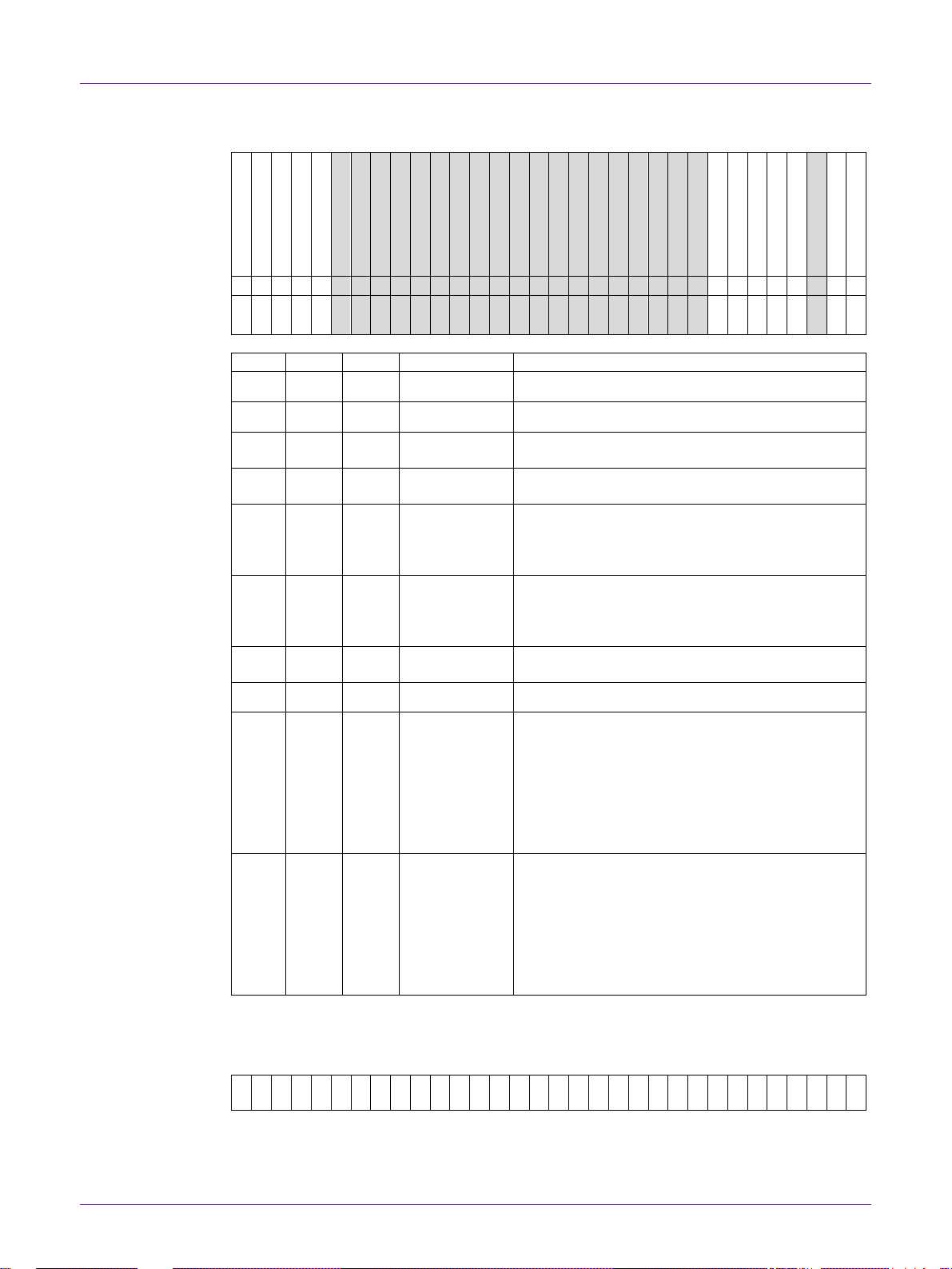
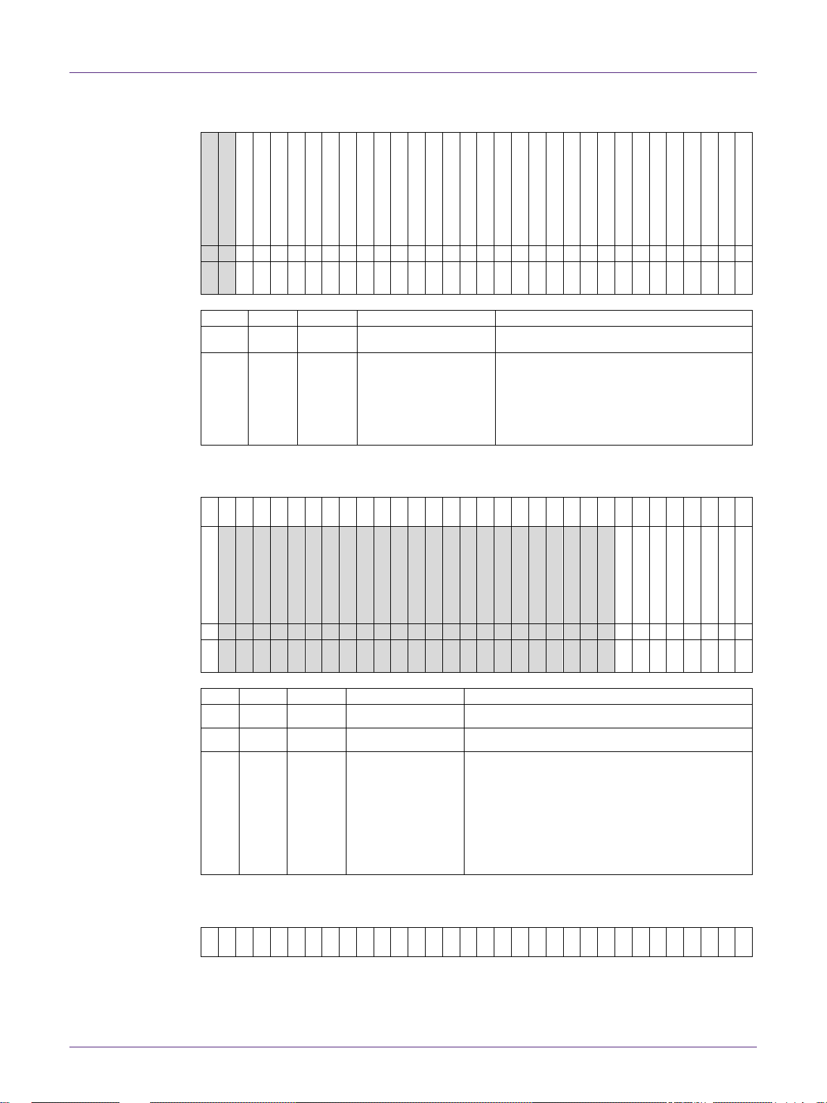
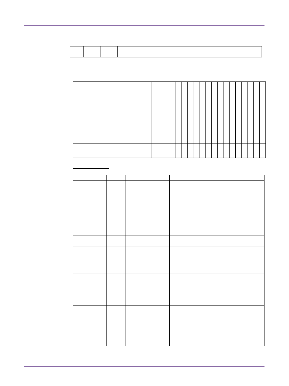
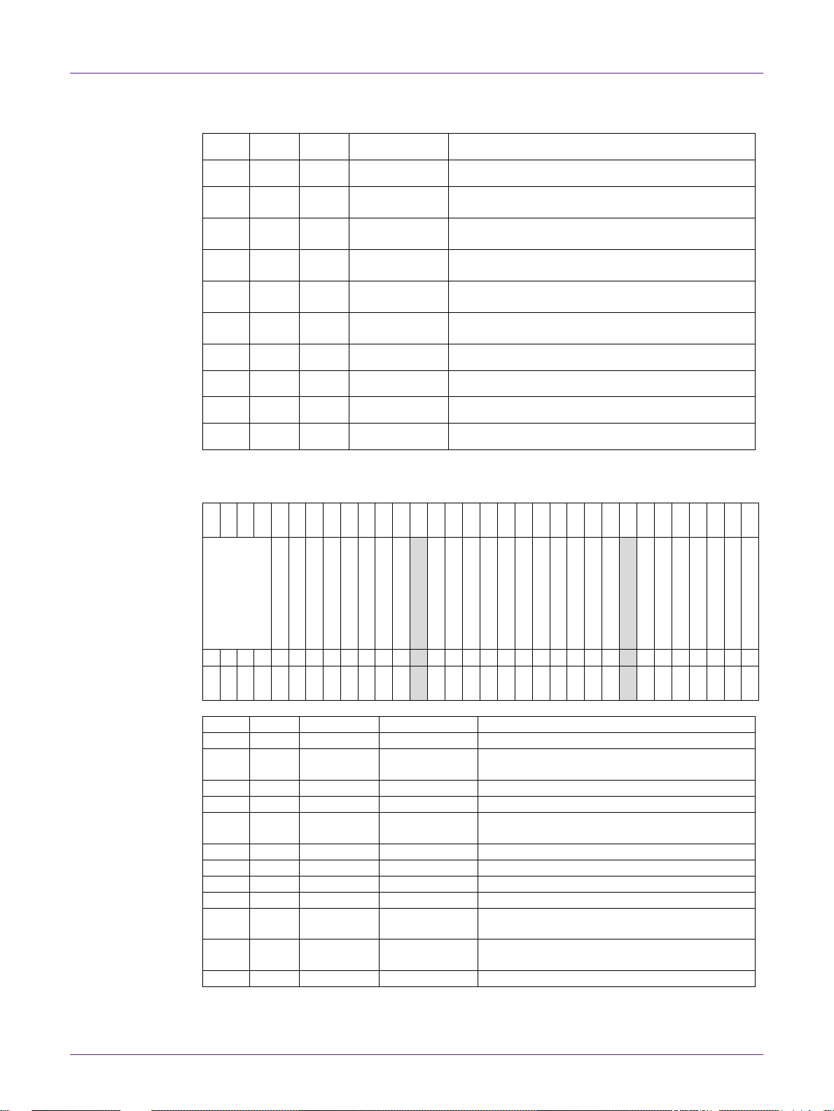
Table 3 CRSS (CLK_RST_SOFT_SET)
31
30
29
28
27
26
25
24
23
22
21
20
19
18
17
16
15
14
13
12
11
10
9 8 7 6 5 4 3 2 1
0
GATING_TIMER3 GATING_TIMER2 GATING_TIMER1 GATING_TIMER0
GATING_UART1 GATING_UART0
GATING_SPI1 GATING_SPI0
GATING_32K_CLK
GATING_SPI_AHB
GATING_GPIO
GATING_ADC
GATING_DMA
GATING_BLE_AHB
GATING_PWM
REBOOT_SYS
LOCKUP_RST
BLE_RST
DP_RST
DPREG_RST
RTC_RST
I2C_RST
GPIO_RST
WDOG_RST
TIMER3_RST TIMER2_RST TIMER1_RST TIMER0_RST
USART1_RST USART0_RST
DMA_RST
CPU_RST
0 0 0 1 1 1 1 1 1 1 1 1 1 1 1 0 0 1 1 1 1 1 1 1 1 1 1 1 1 1 1
1
RW1
RW1
RW1
RW1
RW1
RW1
RW1
RW1
RW1
RW1
RW1
RW1
RW1
RW1
RW1
RW1
RW1
RW1
RW1
RW1
RW1
RW1
RW1
RW1
RW1
RW1
RW1
RW1
RW1
RW1
RW1
RW1
Bit
Type
Reset
Symbol
Description
31
RW1 0 GATING_TIMER3
Write 1 to disable timer 3 clock, 0 no effect.
30
RW1 0 GATING_TIMER2
Write 1 to disable timer 2 clock, 0 no effect.
29
RW1 0 GATING_TIMER1
Write 1 to disable timer 1 clock, 0 no effect.
28
RW1 1 GATING_TIMER0
Write 1 to disable timer 0 clock, 0 no effect.
27
RW1 1 GATING_UART1
Write 1 to disable UART 1 clock, 0 no effect.
26
RW1 1 GATING_UART0
Write 1 to disable UART 0 clock, 0 no effect.
25
RW1 1 GATING_SPI1
Write 1 to disable SPI 1 clock, 0 no effect.
24
RW1 1 GATING_SPI0
Write 1 to disable SPI 0 clock, 0 no effect.
23
RW1 1 GATING_32K_CLK
Write 1 to disable 32KHz clock, 0 no effect.
22
RW1 1 GATING_SPI_AHB
Write 1 to disable FLASH control clock, 0 no effect.
21
RW1 1 GATING_GPIO
Write 1 to disable GPIO clock, 0 no effect.
20
RW1 1 GATING_ADC
Write 1 to disable ADC clock, 0 no effect.
19
RW1 1 GATING_DMA
Write 1 to disable DMA clock, 0 no effect.
18
RW1 1 GATING_BLE_AHB
Write 1 to disable BLE AHB clock, 0 no effect.
17
RW1 1 GATING_PWM
Write 1 to disable PWM clock, 0 no effect.
16
RW1 0 REBOOT_SYS
Write 1 to reboot entire system
15
RW1 0 LOCKUP_RST
Write 1 to enable LOCKUP reset control
14
RW1 1 BLE_RST
Write 1 to set BLE reset
13
RW1 1 DP_RST
Write 1 to set datapath reset
12
RW1 1 DPREG_RST
Write 1 to set datapath register reset
11
RW1 1 RTC_RST
Write 1 to set sleep timer reset
Page 9
NXP Semiconductors
QN902x
User Manual of QN902x
UM10996
All information provided in this document is subject to legal disclaimers.
© NXP Semiconductors N.V. 2018. All rights reserved.
User Manual
Rev 1.3 — 05 November 2018
9 of 128
10
RW1 1 I2C_RST
Write 1 to set I2C reset
9
RW1 1 GPIO_RST
Write 1 to set GPIO reset
8
RW1 1 WDOG_RST
Write 1 to set Watch Dog reset
7
RW1 1 TIMER3_RST
Write 1 to set timer 3 reset
6
RW1 1 TIMER2_RST
Write 1 to set timer 2 reset
5
RW1 1 TIMER1_RST
Write 1 to set timer 1 reset
4
RW1 1 TIMER0_RST
Write 1 to set timer 0 reset
3
RW1 1 USART1_RST
Write 1 to set USART1 (SPI 1 and UART 1) reset
2
RW1 1 USART0_RST
Write 1 to set USART0 (SPI 0 and UART 0) reset
1
RW1 1 DMA_RST
Write 1 to set DMA reset
0
RW1 1 CPU_RST
Write 1 to set CPU reset
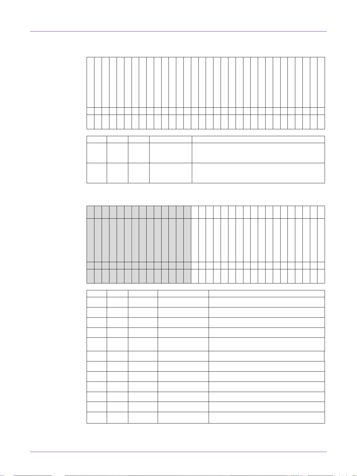
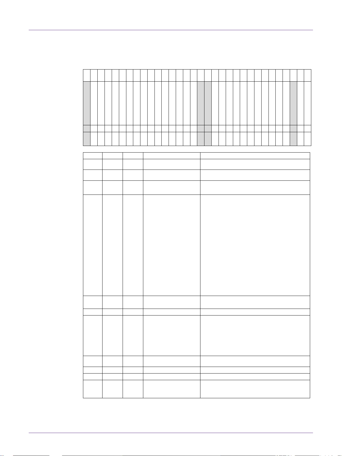
Table 4 CRSC (CLK_RST_SOFT_CLR)
31
30
29
28
27
26
25
24
23
22
21
20
19
18
17
16
15
14
13
12
11
10
9 8 7 6 5 4 3 2 1
0
NGATING_TIMER3 NGATING_TIMER2 NGATING_TIMER1 NGATING_TIMER0
NGATING_UART1 NGATING_UART0
NGATING_SPI1 NGATING_SPI0
NGATING_32K_CLK
NGATING_SPI_AHB
NGATING_GPIO
NGATING_ADC
NGATING_DMA
NGATING_BLE_AHB
NGATING_PWM
RSVD
DIS_LOCKUP_RST
CLR_BLE_RST
CLR_DP_RST
CLR_DPREG_RST
CLR_SLPTIM_RST
CLR_I2C_RST
CLR_GPIO_RST
CLR_WDOG_RST
CLR_TIMER3_RST CLR_TIMER2_RST CLR_TIMER1_RST CLR_TIMER0_RST
CLR_USART1_RST CLR_USART0_RST
CLR_DMA_RST
CLR_CPU_RST
x x x x x x x x x x x x x x x x x x x x x x x x x x x x x x x
x
W1
W1
W1
W1
W1
W1
W1
W1
W1
W1
W1
W1
W1
W1
W1 W1
W1
W1
W1
W1
W1
W1
W1
W1
W1
W1
W1
W1
W1
W1
W1
Bit
Type
Reset
Symbol
Description
31
W1 x NGATING_TIMER3
Write 1 to enable timer 3 clock
30
W1 x NGATING_TIMER2
Write 1 to enable timer 2 clock
29
W1 x NGATING_TIMER1
Write 1 to enable timer 1 clock
28
W1 x NGATING_TIMER0
Write 1 to enable timer 0 clock
27
W1 x NGATING_UART1
Write 1 to enable UART 1 clock
26
W1 x NGATING_UART0
Write 1 to enable UART 0 clock
25
W1 x NGATING_SPI1
Write 1 to enable SPI 1 clock
24
W1 x NGATING_SPI0
Write 1 to enable SPI 0 clock
23
W1 x NGATING_32K_CLK
Write 1 to enable 32KHz clock
22
W1 x NGATING_SPI_AHB
Write 1 to enable SPI AHB clock
21
W1 x NGATING_GPIO
Write 1 to enable GPIO clock
Page 10
NXP Semiconductors
QN902x
User Manual of QN902x
UM10996
All information provided in this document is subject to legal disclaimers.
© NXP Semiconductors N.V. 2018. All rights reserved.
User Manual
Rev 1.3 — 05 November 2018
10 of 128
20
W1 x NGATING_ADC
Write 1 to enable ADC clock
19
W1 x NGATING_DMA
Write 1 to enable DMA clock
18
W1 x NGATING_BLE_AHB
Write 1 to enable BLE AHB clock
17
W1 x NGATING_PWM
Write 1 to enable PWM clock
16 x
RSVD
Reserved
15
W1 x DIS_LOCKUP_RST
Write 1 to disable LOCKUP reset control
14
W1 x CLR_BLE_RST
Write 1 to clear BLE reset
13
W1 x CLR_DP_RST
Write 1 to clear datapath reset
12
W1 x CLR_DPREG_RST
Write 1 to clear datapath register reset
11
W1 x CLR_SLPTIM_RST
Write 1 to clear sleep timer reset
10
W1 x CLR_I2C_RST
Write 1 to clear I2C reset
9
W1 x CLR_GPIO_RST
Write 1 to clear GPIO reset
8
W1 x CLR_WDOG_RST
Write 1 to clear Watch Dog reset
7
W1 x CLR_TIMER3_RST
Write 1 to clear timer 3 reset
6
W1 x CLR_TIMER2_RST
Write 1 to clear timer 2 reset
5
W1 x CLR_TIMER1_RST
Write 1 to clear timer 1 reset
4
W1 x CLR_TIMER0_RST
Write 1 to clear timer 0 reset
3
W1 x CLR_USART1_RST
Write 1 to clear USART1 (SPI 1 and UART 1) reset
2
W1 x CLR_USART0_RST
Write 1 to clear USART0 (SPI 0 and UART 0) reset
1
W1 x CLR_DMA_RST
Write 1 to clear DMA reset
0
W1 x CLR _CPU_RST
Write 1 to clear CPU reset
Table 5 CMDCR (CLK_MUX_DIV_CTRL)
31
30
29
28
27
26
25
24
23
22
21
20
19
18
17
16
15
14
13
12
11
10
9 8 7 6 5 4 3 2 1
0
CLK_MUX[1] CLK_MUX[0]
SEL_CLK_32K
BLE_FRQ_SEL
BLE_DIV_BYPASS
BLE_DIVIDER
AHB_DIV_BYPASS
AHB_DIVIDER
USART1_DIV_BYPASS
USART1_DIVIDER
USART0_DIV_BYPASS
USART0_DIVIDER
RSVD
APB_DIV_BYPASS
APB_DIVIDER
TIMER_DIV_BYPASS
TIMER_DIVIDER
0 1 0 1 1 0 1 0 0 0 0 0 0 0 0 0 0 0 0 1 1 0 0 0 0 0 0 1 1 0 0
1
RW
RW
RW
RW
RW
RW
RW
RW
RW
RW
RW
RW
RW
RW
RW
RW
RW
RW
RW
RW
RW
RW
RW
RW R RW
RW
RW
RW
RW
RW
RW
Bit
Type
Reset
Symbol
Description
Page 11
NXP Semiconductors
QN902x
User Manual of QN902x
UM10996
All information provided in this document is subject to legal disclaimers.
© NXP Semiconductors N.V. 2018. All rights reserved.
User Manual
Rev 1.3 — 05 November 2018
11 of 128
31-
30
RW
01b
CLK_MUX[1-0]
Select system clock source.
00b = High frequency crystal 16MHz or 32MHz;
01b = 20MHz internal high frequency;
10b = 32MHz PLL output;
11b = 32KHz low speed clock;
29
RW 0 SEL_CLK_32K
1 = Select 32KHz clock from RCO
0 = Select 32KHz clock from XTAL32
28
RW 1 BLE_FRQ_SEL
Describe BLE clock frequency.
0 = 8 MHz;
1 = 16 MHz
27
RW 1 BLE_DIV_BYPASS
‘1’ is bypass BLE Divider; Only 16 or 8 MHz are supported;
26
RW 0 BLE_DIVIDER
If BLE_DIV_BYPASS is ‘0’,
BLE_CLK = AHB_CLK / (2*(BLE_DIVIDER +1));
Only 16 or 8 MHz are supported;
25
RW 1 AHB_DIV_BYPASS
‘1’ is bypass AHB Divider;
24-
16
RW 0 AHB_DIVIDER[8-0]
If AHB_DIV_BYPASS is ‘0’,
AHB_CLK = SYS_CLK/(2*(APB_DIVIDER+1));
15
RW 0 USART1_DIV_BYPASS
‘1’ is bypass USART1 Divider;
14-
12
RW
001b
USART1_DIVIDER[2-
0]
If USART1_DIV_BYPASS is ‘0’,
USART1_CLK = AHB_CLK/(2*(USART1_DIVIDER+1))
11
RW 1 USART0_DIV_BYPASS
‘1’ is bypass USART0 Divider;
10-8 RW 0 USART0_DIVIDER[2-
0]
If USART0_DIV_BYPASS is ‘0’,
USART0_CLK = AHB_CLK/(2*(USART1_DIVIDER+1))
7 R 0
RSVD
Reserved
6
RW 0 APB_DIV_BYPASS
‘1’ is bypass APB Divider;
5-4
RW
01b
APB_DIVIDER[1-0]
If APB_DIV_BYPASS is ‘0’,
APB_CLK = AHB_CLK/(2*(APB_DIVIDER+1))
3
RW 1 TIMER_DIV_BYPASS
‘1’ is bypass TIMER Divider;
2-0
RW
001b
TIMER_DIVIDER[2-0]
If TIMER_DIV_BYPASS is ‘0’,
TIMER_CLK = AHB_CLK / (2*(TIMER_DIVIDER + 1));
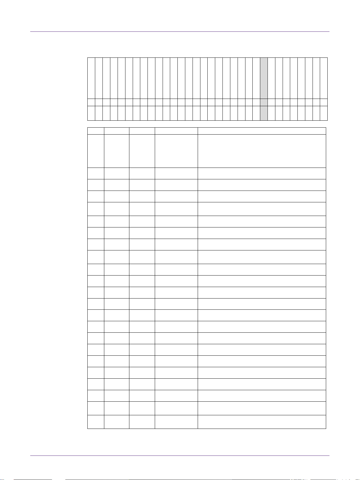
Table 6 STCR (SYS_TICK_CTRL)
31
30
29
28
27
26
25
24
23
22
21
20
19
18
17
16
15
14
13
12
11
10
9 8 7 6 5 4 3 2 1
0
STCLEN
RSVD
RSVD
RSVD
RSVD
RSVD
STCALIB
1 0 0 0 0 0 0 1 0 0 0 0 0 0 0 0 0 0 0 0 0 0 0 1 0 1 0 0 0 1 1
1
RW
R R R R R
RW
RW
RW
RW
RW
RW
RW
RW
RW
RW
RW
RW
RW
RW
RW
RW
RW
RW
RW
RW
RW
RW
RW
RW
RW
RW
Bit
Type
Reset
Symbol
Description
31
RW
1
STCLEN
‘1’ is enable STCLKEN, so that SCLK of CPU can be gated by
STCLKEN;
30-26
R
00000
RSVD
Reserved
Page 12
NXP Semiconductors
QN902x
User Manual of QN902x
UM10996
All information provided in this document is subject to legal disclaimers.
© NXP Semiconductors N.V. 2018. All rights reserved.
User Manual
Rev 1.3 — 05 November 2018
12 of 128
25-0
RW
10001
47h
STCALIB[2
5-0]
CPU STCALIB input
Table 7 PMCR0 (PIN_MUX_CTRL0)
31
30
29
28
27
26
25
24
23
22
21
20
19
18
17
16
15
14
13
12
11
10
9 8 7 6 5 4 3 2 1
0
PIN_CTRL
[31]
PIN_CTRL[30] PIN_CTRL[29] PIN_CTRL[28] PIN_CTRL[27] PIN_CTRL[26] PIN_CTRL[25] PIN_CTRL[24] PIN_CTRL[23] PIN_CTRL[22] PIN_CTRL[21] PIN_CTRL[20] PIN_CTRL[19] PIN_CTRL[18] PIN_CTRL[17] PIN_CTRL[16] PIN_CTRL[15] PIN_CTRL[14] PIN_CTRL[13] PIN_CTRL[12] PIN_CTRL[11] PIN_CTRL[10]
PIN_CTRL[9] PIN_CTRL[8] PIN_CTRL[7] PIN_CTRL[6] PIN_CTRL[5] PIN_CTRL[4] PIN_CTRL[3] PIN_CTRL[2]
PIN_CTR[1]
PIN_CTRL[0]
0 0 0 0 0 0 0 0 0 0 0 0 0 0 0 0 0 0 0 0 0 0 0 0 0 0 0 0 0 0 0
0
RW
RW
RW
RW
RW
RW
RW
RW
RW
RW
RW
RW
RW
RW
RW
RW
RW
RW
RW
RW
RW
RW
RW
RW
RW
RW
RW
RW
RW
RW
RW
RW
Bit
Type
Reset
Symbol
Description
31-0
RW 0 PIN_CTRL[31-0]
Please see GPIO MUX Table;
Table 8 PMCR1 (PIN_MUX_CTRL1)
31
30
29
28
27
26
25
24
23
22
21
20
19
18
17
16
15
14
13
12
11
10
9 8 7 6 5 4 3 2 1
0
FLASH_CTRL_PIN
TEST_ENABLE1 TEST_ENABLE0
PIN_CTRL[60] PIN_CTRL[59] PIN_CTRL[58] PIN_CTRL[57] PIN_CTRL[56] PIN_CTRL[55] PIN_CTRL[54] PIN_CTRL[53] PIN_CTRL[52] PIN_CTRL[51] PIN_CTRL[50] PIN_CTRL[49] PIN_CTRL[48] PIN_CTRL[47] PIN_CTRL[46] PIN_CTRL[45] PIN_CTRL[44] PIN_CTRL[43] PIN_CTRL[42] PIN_CTRL[41] PIN_CTRL[40] PIN_CTRL[39] PIN_CTRL[38] PIN_CTRL[37] PIN_CTRL[36] PIN_CTRL[35] PIN_CTRL[34] PIN_CTRL[33] PIN_CTRL[32]
0 0 0 0 0 0 0 0 0 0 0 0 0 0 0 0 0 0 0 0 0 0 0 0 0 0 0 0 0 0 0
0
RW
RW
RW
RW
RW
RW
RW
RW
RW
RW
RW
RW
RW
RW
RW
RW
RW
RW
RW
RW
RW
RW
RW
RW
RW
RW
RW
RW
RW
RW
RW
RW
Bit
Type
Reset
Symbol
Description
31
RW
0
FLASH_CTRL_PIN
When External Flash is used,
0 = P1_0,P1_1,P1_2,P1_3 port is for SPI Flash;
1 = P1_0,P1_1,P1_2,P1_3port isn’t for SPI Flash;
30
RW
0
TEST_ENABLE1
Reserved. Must write 0.
29
RW
0
TEST_ENABLE0
Reserved. Must write 0.
28-0
RW
0
PIN_CTRL[60-32]
Please see GPIO MUX Table;
Table 9 PMCR2 (PIN_MUX_CTRL2)
31
30
29
28
27
26
25
24
23
22
21
20
19
18
17
16
15
14
13
12
11
10
9 8 7 6 5 4 3 2 1
0
Page 13
NXP Semiconductors
QN902x
User Manual of QN902x
UM10996
All information provided in this document is subject to legal disclaimers.
© NXP Semiconductors N.V. 2018. All rights reserved.
User Manual
Rev 1.3 — 05 November 2018
13 of 128
TEST_CTRL[4] TEST_CTRL[3] TEST_CTRL[2] TEST_CTRL[1] TEST_CTRL[0]
RSVD
RSVD
RSVD
RSVD
RSVD
RSVD
RSVD
RSVD
RSVD
RSVD
RSVD
RSVD
RSVD
RSVD
RSVD
RSVD
RSVD
RSVD
RSVD
CLKOUT1_PIN_SEL CLKOUT0_PIN_SEL
UART1_PIN_SEL
I2C_PIN_SEL
ADCT_PIN_SEL
RSVD
SPI0_PIN_SEL SPI1_PIN_SEL
0 0 0 0 0 0 0 0 0 0 0 0 0 0 0 0 0 0 0 0 0 0 0 0 1 0 0 0 0 0 0
0
RW
RW
RW
RW
RW
R R R R R R R R R R R R R R R R R R R
RW
RW
RW
RW
RW R RW
RW
Bit
Type
Reset
Symbol
Description
31-27
RW
0
TEST_CTRL[4-0]
Reserved
26-8 R 0
RSVD
Reserved
7
RW
1
CLKOUT1_PIN_S
EL
0 = CLKOUT1 is HCLK;
1 = CLKOUT1 is CLK_32K
6
RW
0
CLKOUT0_PIN_S
EL
0 = CLKOUT0 is HCLK;
1 = CLKOUT0 is CLK_32K
5
RW
0
UART1_PIN_SEL
0 = UART1_cts is connected with P1_2;
UART1_rxd is connected with P1_0;
1 = UART1_cts is connected with P3_7;
UART1_rxd is connected with P2_0;
4
RW
0
I2C_PIN_SEL
0 = i2c_scl is connected with P2_4;
I2c_sda is connected with P2_3;
1 = i2c_scl is connected with P0_5;
I2c_sda is connected with P0_2;
3
RW
0
ADCT_PIN_SEL
0 = ADC Trigger is connected with P1_2;
1 = ADC Trigger is connected with P0_5;
2 R 0
RSVD
Reserved
1
RW
0
SPI0_PIN_SEL
0 = SPI 0 CLK is connected with P0_2;
SPI 0 CS0 is connected with P0_1;
SPI 0 Data out is connected with P0_0;
SPI 0 Data in is connected with P1_7;
1 = SPI 0 CLK is connected with P3_5;
SPI 0 CS0 is connected with P3_6;
SPI 0 Data out is connected with P3_4;
SPI 0 Data in is connected with P3_3;
0
RW
0
SPI1_PIN_SEL
0 = SPI 1 CLK is connected with P1_3;
SPI 1 CS0 is connected with P1_2;
SPI 1 Data out is connected with P1_1;
SPI 1 Data in is connected with P1_0;
1 = SPI 1 CLK is connected with P2_2;
SPI 1 CS0 is connected with P3_7;
SPI 1 Data out is connected with P2_1;
SPI 1 Data in is connected with P2_0;
Table 10 PDCR (PAD_DRV_CTRL)
31
30
29
28
27
26
25
24
23
22
21
20
19
18
17
16
15
14
13
12
11
10
9 8 7 6 5 4 3 2 1
0
Page 14
NXP Semiconductors
QN902x
User Manual of QN902x
UM10996
All information provided in this document is subject to legal disclaimers.
© NXP Semiconductors N.V. 2018. All rights reserved.
User Manual
Rev 1.3 — 05 November 2018
14 of 128
RSVD
PAD_DRV_CTRL[30] PAD_DRV_CTRL[29] PAD_DRV_CTRL[28] PAD_DRV_CTRL[27] PAD_DRV_CTR
L[26]
PAD_DRV_CTRL[25] PAD_DRV_CTRL[24] PAD_DRV_CTRL[23] PAD_DRV_CTRL[22] PAD_DRV_CTRL[21] PAD_DRV_CTRL[20] PAD_DRV_CTRL[19] PAD_DRV_CTRL[18] PAD_DRV_CTRL[17] PAD_DRV_CTRL[16] PAD_DRV_CTRL[15] PAD_DRV_CTRL[14] PAD_DRV_CTRL[13] PAD_DRV_CTRL[12] PAD_DRV_CTRL
[11]
PAD_DRV_CTRL[10]
PAD_DRV_CTRL[9] PAD_DRV_CTRL[8] PAD_DRV_CTRL[7] PAD_DRV_CTRL[6] PAD_DRV_CTRL[5] PAD_DRV_CTRL[4] PAD_DRV_CTRL[3] PAD_DRV_CTRL[2] PAD_DRV_CTRL[1] PAD_DRV_CTRL[0]
0 0 0 0 0 0 0 0 0 0 0 0 0 0 0 0 0 0 0 0 0 0 0 0 0 0 0 0 0 0 0
0
R
RW
RW
RW
RW
RW
RW
RW
RW
RW
RW
RW
RW
RW
RW
RW
RW
RW
RW
RW
RW
RW
RW
RW
RW
RW
RW
RW
RW
RW
RW
RW
Bit
Type Res
et
Symbol
Description
31 R 0
RSVD
Reserved
30-0
RW 0 PAD_DRV_CTRL[
30-0]
Every bit control one GPIO PAD driver ability;
0 = Low driver ,
1 = High driver.
Table 11 PPCR0 (PAD_PULL_CTRL0)
31
30
29
28
27
26
25
24
23
22
21
20
19
18
17
16
15
14
13
12
11
10
9 8 7 6 5 4 3 2 1
0
PAD_PULL_CTRL[31] PAD_PULL_CTRL[30] PAD_PULL_CTRL[29] PAD_PULL_CTRL[28] PAD_PULL_CTRL[27] PAD_PULL_CTRL[26] PAD_PULL_CTRL[25] PAD_PULL_CTRL[24] PAD_PULL_CTRL[23] PAD_PULL_CTRL[22] PAD_PULL_CTRL[21] PAD_PULL_CTRL[20] PAD_PULL_CTRL[19] PAD_PULL_CTRL[18] PAD_PULL_CTRL[17] PAD_PULL_CTRL[16] PAD_PULL_CTRL[15] PAD_PULL_CTRL[14] PAD_PULL_CTRL[13] PAD_PULL_CTRL[12] PAD_PULL_CTRL[11] PAD_PULL_CTRL[10]
PAD_PULL_CTRL[9] PAD_PULL_CTRL[8] PAD_PULL_CTRL[7] PAD_PULL_CTRL[6] PAD_PULL_CTRL[5] PAD_PULL_CTRL[4] PAD_PULL_CTRL[3] PAD_PULL_CTRL[2] PAD_PULL_CTRL[1] PAD_PULL_CTRL[0]
1 0 1 0 1 0 1 0 1 0 1 0 1 0 1 0 1 0 1 0 1 0 1 0 1 0 1 0 1 0 1
0
RW
RW
RW
RW
RW
RW
RW
RW
RW
RW
RW
RW
RW
RW
RW
RW
RW
RW
RW
RW
RW
RW
RW
RW
RW
RW
RW
RW
RW
RW
RW
RW
Bit
Type
Reset
Symbol
Description
31-0
RW
AAAA
AAAA
h
PAD_PULL_CTRL[31-0]
Every two bit control one GPIO PAD Pull Up or
Pull Down;
00b = High-Z;
01b = Pull-down;
10b = Pull-up;
11b = Reserved
Table 12 PPCR1 (PAD_PULL_CTRL1)
31
30
29
28
27
26
25
24
23
22
21
20
19
18
17
16
15
14
13
12
11
10
9 8 7 6 5 4 3 2 1
0
Page 15
NXP Semiconductors
QN902x
User Manual of QN902x
UM10996
All information provided in this document is subject to legal disclaimers.
© NXP Semiconductors N.V. 2018. All rights reserved.
User Manual
Rev 1.3 — 05 November 2018
15 of 128
RSVD
RSVD
PAD_PULL_CTRL[62] PAD_PULL_CTRL[61] PAD_PULL_CTRL[60] PAD_PULL_CTRL[59] PAD_PULL_CTRL[58] PAD_PULL_CTRL[57] PAD_PULL_CTRL[56] PAD_PULL_CTRL[55] PAD_PULL_CTRL[54] PAD_PULL_CTRL[53] PAD_PULL_CTRL[52] PAD_PULL_CTRL[51] PAD_PULL_CTRL[50] PAD_PULL_CTRL[49] PAD_PULL_CTRL[48] PAD_PULL_CTRL[47] PAD_PULL_CTRL[46] PAD_PULL_CTRL[45] PAD_PULL_CTRL[44] PAD_PULL_CTRL[43] PAD_PULL_CTRL[42] PAD_PULL_CTRL[41] PAD_PULL_CTRL[40] PAD_PULL_CTRL[39] PAD_PULL_CTRL[37] PAD_PULL_CTRL[36] PAD_PULL_CTRL[35] PAD_PULL_CTRL[34] PAD_PULL_CTRL[33] PAD_PULL_CTRL[32]
0 0 1 0 1 0 1 0 1 0 1 0 1 0 1 0 1 0 1 0 1 0 1 0 1 0 1 0 1 0 1
0
R
R
RW
RW
RW
RW
RW
RW
RW
RW
RW
RW
RW
RW
RW
RW
RW
RW
RW
RW
RW
RW
RW
RW
RW
RW
RW
RW
RW
RW
RW
RW
Bit
Type
Reset
Symbol
Description
31-30 R 0
RSVD
Reserved
29-0
RW
2AAAAA
AAh
PAD_PULL_CTRL[62-32]
Every two bit control one GPIO PAD Pull Up or
Pull Down;
00b = High-Z;
01b = Pull-down;
10b = Pull-up;
11b = Reserved
Table 13 RCS (RST_CAUSE_SRC)
31
30
29
28
27
26
25
24
23
22
21
20
19
18
17
16
15
14
13
12
11
10
9 8 7 6 5 4 3 2 1
0
RST_CAUSE_CLR
RSVD
RSVD
RSVD
RSVD
RSVD
RSVD
RSVD
RSVD
RSVD
RSVD
RSVD
RSVD
RSVD
RSVD
RSVD
RSVD
RSVD
RSVD
RSVD
RSVD
RSVD
RSVD
RSVD
RST_CAUSE[7] RST_CAUSE[6] RST_CAUSE[5] RST_CAUSE[4] RST_CAUSE[3] RST_CAUSE[2] RST_CAUSE[1] RST_CAUSE[0]
0 0 0 0 0 0 0 0 0 0 0 0 0 0 0 0 0 0 0 0 0 0 0 0 x x x x x x x
x
W1
R R R R R R R R R R R R R R R R R R R R R R R R R R R R R R R
Bit
Type
Reset
Symbol
Description
31
W1 0 RST_CAUSE_CLR
Write ‘1’ clear RESET_CAUSE bits;
30-8 R 0
RSVD
Reserved
7-0 R x
RST_CAUSE[7-0]
xxxxxxx1b = Power-on Reset;
xxxxxx1xb = Brown-Down Reset;
xxxxx1xxb = External pin Reset;
xxxx1xxxb = Watch Dog Reset;
xxx1xxxxb = Lock Up Reset;
xx1xxxxxb = Reboot Reset;
x1000000b = CPU system Reset requirement;
10000000b = CPU software Reset;
Table 14 IOWCR (IO_WAKEUP_CTRL)
31
30
29
28
27
26
25
24
23
22
21
20
19
18
17
16
15
14
13
12
11
10
9 8 7 6 5 4 3 2 1
0
Page 16
NXP Semiconductors
QN902x
User Manual of QN902x
UM10996
All information provided in this document is subject to legal disclaimers.
© NXP Semiconductors N.V. 2018. All rights reserved.
User Manual
Rev 1.3 — 05 November 2018
16 of 128
IO_VALUE[15] IO_VALUE[14] IO_VALUE[13] IO_VALUE[12] IO_VALUE[11] IO_VALUE[10]
IO_VALUE[9] IO_VALUE[8] IO_VALUE[7] IO_VALUE[6] IO_VALUE[5] IO_VALUE[4] IO_VALUE[3] IO_VALUE[2] IO_VALUE[1] IO_VALUE[0]
IO_WAKEUP_EN[15] IO_WAKEUP_EN[14] IO_WAKEUP_EN[13] IO_WAKEUP_EN[12] IO_WAKEUP_EN[11] IO_WAKEUP_EN[10]
IO_WAKEUP_EN[9] IO_WAKEUP_EN[8] IO_WAKEUP_EN[7] IO_WAKEUP_EN[6] IO_WAKEUP_EN[5] IO_WAKEUP_EN[4] IO_WAKEUP_EN[3] IO_WAKEUP_EN[2] IO_WAKEUP_EN[1] IO_WAKEUP_EN[0]
0 0 0 0 0 0 0 0 0 0 0 0 0 0 0 0 0 0 0 0 0 0 0 0 0 0 0 0 0 0 0
0
RW
RW
RW
RW
RW
RW
RW
RW
RW
RW
RW
RW
RW
RW
RW
RW
RW
RW
RW
RW
RW
RW
RW
RW
RW
RW
RW
RW
RW
RW
RW
RW
Bit
Type
Reset
Symbol
Description
31-16
RW
0
IO_VALUE[15-0]
Control GPIO 0 ~ 15 Interrupt cause;
0 = When GPIO x is 1, generate interrupt;
1 = When GPIO x is 0, generate interrupt;
15-0
RW
0
IO_WAKEUP_E
N[15-0]
Control GPIO 0 ~ 15 as Wakeup source;
0 = Disable GPIO x as Wakeup source;
1 = Enable GPIO x as Wakeup source;
Table 15 BLESR (BLE_STATUS)
31
30
29
28
27
26
25
24
23
22
21
20
19
18
17
16
15
14
13
12
11
10
9 8 7 6 5 4 3 2 1
0
RSVD
RSVD
RSVD
RSVD
RSVD
RSVD
RSVD
RSVD
RSVD
RSVD
RSVD
RSVD
RSVD
RSVD
CLK_RDY
CLK_XTAL32_RDY
REF_PLL_RDY
BG_RDY
BUCK_RDY
TX_EN
RX_EN
OSC_EN
CLK_STATUS
RADIO_EN
FREQ_WORD[7] FREQ_WORD[6] FREQ_WORD[5] FREQ_WORD[4] FREQ_WORD[3] FREQ_WORD[2] FREQ_WORD[1] FREQ_WORD[0]
0 0 0 0 0 0 0 0 0 0 0 0 0 0 0 0 0 0 0 0 0 0 0 0 0 0 0 0 0 0 0
0
R R R R R R R R R R R R R R R R R R R R R R R R R R R R R R R
R
Bit
Type
Reset
Symbol
Description
31-18 R 0
RSVD
Reserved
17 R 0
CLK_RDY
16MHz/32MHz XTAL is ready
16 R 0
CLK_XTAL32_RDY
32KHz XTAL is ready
15 R 0
REF_PLL_RDY
REF PLL is ready
14 R 1
FLSH_LOCATION
1 = Internal Flash
0 = External Flash
13 R 0
BUCK_RDY
BUCK power is ready
12 R 0
TX_EN
QN902X is in transmit state;
11 R 0
RX_EN
QN902X is in receive state;
10 R 0
OSC_EN
BLE IP osc_en output;
9 R 0
CLK_STATUS
BLE IP clk_status output;
8 R 0
RADIO_EN
BLE IP radio_en output;
7-0 R 0
FREQ_WORD[7-0]
BLE Frequency Word;
Page 17
NXP Semiconductors
QN902x
User Manual of QN902x
UM10996
All information provided in this document is subject to legal disclaimers.
© NXP Semiconductors N.V. 2018. All rights reserved.
User Manual
Rev 1.3 — 05 November 2018
17 of 128
Table 16 SMR (SYS_MODE_REG)
31
30
29
28
27
26
25
24
23
22
21
20
19
18
17
16
15
14
13
12
11
10
9 8 7 6 5 4 3 2 1
0
BOOT_MODE
EN_SW_MAP
RSVD
RSVD
RSVD
RSVD
RSVD
RSVD
RSVD
RSVD
RSVD
RSVD
RSVD
RSVD
RSVD
RSVD
RSVD
RSVD
RSVD
RSVD
RSVD
RSVD
RSVD
RSVD
RSVD
RSVD
RAM_BIST_FAIL
RAM_BIST_END
ROM_BIST_FAIL
ROM_BIST_END
BIST_START
TEST_MOD
1 0 0 0 0 0 0 0 0 0 0 0 0 0 0 0 0 0 0 0 0 0 0 0 0 0 0 0 0 0 0
0
RWH
RW
R R R R R R R R R R R R R R R R R R R R R R R R R R R
R
RW
RW
Bit
Type
Reset
Symbol
Description
31
RWH
1
BOOT_MODE
Must write ‘1’
30
RW
0
EN_SW_MAP
1 = Enable SW ReMap;
29-6 R 0
RSVD
Reserved
5 R 0
RAM_BIST_FAIL
Reserved
4 R 0
RAM_BIST_END
Reserved
3 R 0
ROM_BIST_FAIL
Reserved
2 R 0
ROM_BIST_END
Reserved
1
RW
0
BIST_START
Reserved. Must write ‘0’
0
RW
0
TEST_MOD
Reserved. Must write ‘0’
Table 17 CHIP_ID
31
30
29
28
27
26
25
24
23
22
21
20
19
18
17
16
15
14
13
12
11
10
9 8 7 6 5 4 3 2 1
0
RSVD
RSVD
RSVD
RSVD
RSVD
RSVD
RSVD
RSVD
RSVD
RSVD
RSVD
RSVD
RSVD
RSVD
RSVD
RSVD
CHIP_ID[15] CHIP_ID[14] CHIP_ID[13] CHIP_ID[12] CHIP_ID[11] CHIP_ID[10]
CHIP_ID[9] CHIP_ID[8] CHIP_ID[7] CHIP_ID[6] CHIP_ID[5] CHIP_ID[4] CHIP_ID[3] CHIP_ID[2]
CHIP_ID[1] CHIP_ID[0]
0 0 0 0 0 0 0 0 0 0 0 0 0 0 0 0 0 0 1 0 1 0 0 0 0 0 0 0 0 0 0
0
R R R R R R R R R R R R R R R R R R R R R R R R R R R R R R R
R
Bit
Type
Reset
Symbol
Description
31-16 R 0
RSVD
Reserved
15-0 R 2901h
CHIP_ID[15-0]
QN902X CHIP ID
Table 18 PGCR0 (POWER_GATING_CTRL0)
31
30
29
28
27
26
25
24
23
22
21
20
19
18
17
16
15
14
13
12
11
10 9 8 7 6 5 4 3 2 1 0
Page 18
NXP Semiconductors
QN902x
User Manual of QN902x
UM10996
All information provided in this document is subject to legal disclaimers.
© NXP Semiconductors N.V. 2018. All rights reserved.
User Manual
Rev 1.3 — 05 November 2018
18 of 128
SEL_PD
PD_OSC
PD_BG
PD_V2I
PD_BUCK
PD_VREG_A
PD_VREG_D
PD_XTAL
PD_XTAL32
DIV_RST_SYNC
PD_LO_VCO
PD_LO_PLL
PD_PA
PD_LNA
PD_LNA_PKDET
PD_MIXER
PD_PPF_PKDET
PD_PPF
PD_RX_PKDET
PD_RX_ADC
PD_SAR_ADC
PD_RCO
BOND_EN
RSVD
PD_MEM7 PD_MEM6 PD_MEM5 PD_MEM4 PD_MEM3 PD_MEM2 PD_MEM1
PL_VREG_D
1 1 1 1 1 1 1 1 0 1 1 1 1 1 1 1 1 1 1 1 1 0 1 0 0 0 0 0 0 0 0
0
RW
RW
RW
RW
RW
RW
RW
RW
RW
RW
RW
RW
RW
RW
RW
RW
RW
RW
RW
RW
RW
RW
RW R RW
RW
RW
RW
RW
RW
RW
RW
Bit
Type
Reset
Symbol
Description
31
RW
1
SEL_PD
BLE radio sub-block (LO_VCO, …)power control
selection
0 = Controlled by individual register bit, DIS_xxx
1 = Automatically controlled by BLE baseband
hardware
30
RW
1
PD_OSC
Reserved. Must write ‘1’
29
RW
1
PD_BG
Reserved. Must write ‘1’
28
RW
1
PD_V2I
Reserved. Must write ‘1’
27
RW
1
PD_BUCK
While DC-DC enabled, write ‘0’;
While DC-DC disabled, write ‘1’;
26
RW
1
PD_VREG_A
Reserved. Must write ‘1’
25
RW
1
PD_VREG_D
Reserved. Must write ‘1’
24
RW
1
PD_XTAL
Reserved. Must write ‘1’
23
RW
0
PD_XTAL32
1 = Switch off 32KHz XTAL power in sleep mode
0 = Switch on 32KHz XTAL power in sleep mode
22
RW
1
DIV_RST_SYNC
Reserved. Must write ‘1’
21
RW
1
PD_LO_VCO
Reserved. Must write ‘1’
20
RW
1
PD_LO_PLL
Reserved. Must write ‘1’
19
RW
1
PD_PA
Reserved. Must write ‘1’
18
RW
1
PD_LNA
Reserved. Must write ‘1’
17
RW
1
PD_LNA_PKDET
Reserved. Must write ‘1’
16
RW
1
PD_MIXER
Reserved. Must write ‘1’
15
RW
1
PD_PPF_PKDET
Reserved. Must write ‘1’
14
RW
1
PD_PPF
Reserved. Must write ‘1’
13
RW
1
PD_RX_PKDET
Reserved. Must write ‘1’
12
RW
1
PD_RX_ADC
Reserved. Must write ‘1’
11
RW
1
PD_SAR_ADC
Reserved. Must write ‘1’
10
RW
0
PD_RCO
1 = Switch off 32KHz RC power in sleep mode
0 = Switch on 32KHz RC power in sleep mode
9
RW
1
BOND_EN
1 = Enable bond option;
0 = Disable bond option;
Page 19
NXP Semiconductors
QN902x
User Manual of QN902x
UM10996
All information provided in this document is subject to legal disclaimers.
© NXP Semiconductors N.V. 2018. All rights reserved.
User Manual
Rev 1.3 — 05 November 2018
19 of 128
Must write 1 for QN9020 and QN9021; can keep 0 for
QN9022.
8 R 0
RSVD
Reserved
7
RW
0
PD_MEM7
1 = Switch off memory 7 power in sleep mode
0 = Switch on memory 7 power in sleep mode
6
RW
0
PD_MEM6
1 = Switch off memory 6 power in sleep mode
0 = Switch on memory 6 power in sleep mode
5
RW
0
PD_MEM5
1 = Switch off memory 5 power in sleep mode
0 = Switch on memory 5 power in sleep mode
4
RW
0
PD_MEM4
1 = Switch off memory 4 power in sleep mode
0 = Switch on memory 4 power in sleep mode
3
RW
0
PD_MEM3
1 = Switch off memory 3 power in sleep mode
0 = Switch on memory 3 power in sleep mode
2
RW
0
PD_MEM2
1 = Switch off memory 2 power in sleep mode
0 = Switch on memory 2 power in sleep mode
1
RW
0
PD_MEM1
1 = Switch off memory 1 power in sleep mode
0 = Switch on memory 1 power in sleep mode
0
RW
0
PL_VREG_D
Low power mode, write ‘0’. Otherwise, write ‘1’
Table 19 PGCR1 (POWER_GATING_CTRL1)
31
30
29
28
27
26
25
24
23
22
21
20
19
18
17
16
15
14
13
12
11
10 9 8 7 6 5 4 3 2 1 0
VDD_RCO_SET
DIS_OSC
DIS_BG
DIS_V2I
DIS_BUCK
DIS_VREG_A
DIS_VREG_D
DIS_XTAL
DIS_XTAL32
DIS_REF_PLL DIS_LO_VCO
DIS_LO_PLL
DIS_PA
DIS_LNA
DIS_LNA_PKDET
DIS_MIXER
DIS_PPF_PKDET
DIS_PPF
DIS_RX_PKDET
DIS_RX_ADC
DIS_SAR_ADC
DIS_RCO
RSVD
RSVD
DIS_MEM7 DIS_MEM6 DIS_MEM5 DIS_MEM4 DIS_MEM3 DIS_MEM2 DIS_MEM1
DIS_SAR_BUF
1 0 0 0 0 0 0 0 0 1 1 1 1 1 1 1 1 1 1 1 1 1 0 0 0 0 0 0 0 0 0
0
RWW RW
RW
RW
RW
RW
RW
RW
RW
RW
RW
RW
RW
RW
RW
RW
RW
RW
RW
RW
RW
RW
R
R
RW
RW
RW
RW
RW
RW
RW
RW
Bit
Type
Reset
Symbol
Description
31
RW
1
VDD_RCO_SET
1 = Set RCO VDD high
0 = Set RCO VDD low (~200mV difference)
30
RW
0
DIS_OSC
1 = Switch off 40MHz oscillator power
0 = Switch on 40MHz oscillator power
29
RW
0
DIS_BG
1 = Switch off bandgap power
0 = Switch on bandgap power
28
RW
0
DIS_V2I
1 = Switch off IVREF power
0 = Switch on IVREF power
27
RW
0
DIS_BUCK
1 = Switch off buck converter power
0 = Switch on buck converter power
26
RW
0
DIS_VREG_A
1 = Switch off VREG of analog power
0 = Switch on VREG of analog power
25
RW
0
DIS_VREG_D
1 = Switch off VREG of digital power
0 = Switch on VREG of digital power
24
RW
0
DIS_XTAL
1 = Switch off 16/32MHz XTAL power
0 = Switch on 16/32MHz XTAL power
23
RW
0
DIS_XTAL32
1 = Switch off 32KHz XTAL power
0 = Switch on 32KHz XTAL power
Page 20

NXP Semiconductors
QN902x
User Manual of QN902x
UM10996
All information provided in this document is subject to legal disclaimers.
© NXP Semiconductors N.V. 2018. All rights reserved.
User Manual
Rev 1.3 — 05 November 2018
20 of 128
22
RW
1
DIS_REF_PLL
1 = Switch off REF PLL power
0 = Switch on REF PLL power
21
RW
1
DIS_LO_VCO
LO VCO power control, only effective when SEL_PD=0
1 = Switch off VCO of LO PLL power
0 = Switch on VCO of LO PLL power
20
RW
1
DIS_LO_PLL
LO VCO power control, only effective when SEL_PD=0
1 = Switch off LO PLL power
0 = Switch on LO PLL power
19
RW
1
DIS_PA
LO VCO power control, only effective when SEL_PD=0
1 = Switch off Tx PA power
0 = Switch on Tx PA power
18
RW
1
DIS_LNA
LO VCO power control, only effective when SEL_PD=0
1 = Switch off Rx LNA power
0 = Switch on Rx LNA power
17
RW
1
DIS_LNA_PKDET
LO VCO power control, only effective when SEL_PD=0
1 = Switch off Rx LNA peak detector power
0 = Switch on Rx LNA peak detector power
16
RW
1
DIS_MIXER
LO VCO power control, only effective when SEL_PD=0
1 = Switch off Rx MIXER power
0 = Switch on Rx MIXER power
15
RW
1
DIS_PPF_PKDET
LO VCO power control, only effective when SEL_PD=0
1 = Switch off Rx PPF peak detector power
0 = Switch on Rx PPF peak detector power
14
RW
1
DIS_PPF
LO VCO power control, only effective when SEL_PD=0
1 = Switch off Rx PPF power
0 = Switch on Rx PPF power
13
RW
1
DIS_RX_PKDET
LO VCO power control, only effective when SEL_PD=0
1 = Switch off Rx peak detector 3 power
0 = Switch on Rx peak detector 3 power
12
RW
1
DIS_RX_ADC
LO VCO power control, only effective when SEL_PD=0
1 = Switch off Rx ADC power
0 = Switch on Rx ADC power
11
RW
1
DIS_SAR_ADC
1 = Switch off SAR ADC power
0 = Switch on SAR ADC power
10
RW
1
DIS_RCO
1 = Switch off 32KHz RC power
0 = Switch on 32KHz RC power
9 R 0
RSVD
Reserved
8 R 0
RSVD
Reserved
7
RW
0
DIS_MEM7
1 = Switch off memory 7 power
0 = Switch on memory 7 power
6
RW
0
DIS_MEM6
1 = Switch off memory 6 power
0 = Switch on memory 6 power
5
RW
0
DIS_MEM5
1 = Switch off memory 5 power
0 = Switch on memory 5 power
4
RW
0
DIS_MEM4
1 = Switch off memory 4 power
0 = Switch on memory 4 power
3
RW
0
DIS_MEM3
1 = Switch off memory 3 power
0 = Switch on memory 3 power
2
RW
0
DIS_MEM2
1 = Switch off memory 2 power
0 = Switch on memory 2 power
1
RW
0
DIS_MEM1
1 = Switch off memory 1 power
0 = Switch on memory 1 power
Page 21
NXP Semiconductors
QN902x
User Manual of QN902x
UM10996
All information provided in this document is subject to legal disclaimers.
© NXP Semiconductors N.V. 2018. All rights reserved.
User Manual
Rev 1.3 — 05 November 2018
21 of 128
0
RW
0
DIS_SAR_BUF
1 = Switch off SAR buffer
0 = Switch on SAR buffer
Table 20 PGCR2 (POWER_GATING_CTRL2)
Description of Word
Bit
Type
Reset
Name
Description
31-18 R 0h
RSVE
17-16
RW
01b
VREG12_A_BAK[1-0]
1.2V regulator for analog output voltage selection
11 = 1.3V
10 = 1.2V
01 = 1.1V
00 = 1.0V
15-9 R 0
RSVE
Reserved
8
RW 1 OSC_WAKEUP_EN
1 is Enable OSC_EN as wakeup source
7
RW 0 RTCI_PIN_SEL
0 = RTC Capture is connected with P0_0;
1 = RTC Capture is connected with P0_4;
6
RW 0 PD_STATE
Enable or disable wakeup source selection. Write
‘1’ before entering sleep mode. Write ‘0’ after
wakeup.
0 = Normal;
1 = Sleep;
5
RW 0 BD_AMP_EN
1 is Enable comparator of brown-out detector. It
should be set earlier than EN_BD 2us or more.
4
RW 0 DVDD12_PMU_SET
Write ‘1’ before entering sleep mode. Write ‘0’
after wakeup.
0 = High VDD_PMU in sleep mode
1 = Low VDD_PMU in sleep mode
3
RW 0 RX_EN_SEL
Reserved, must write ‘1’;
2
RW 1 FLASH_VCC_EN
1 = Open Flash Power;
0 = Close Flash Power;
1
RW 1 PMUENABLE
1 = Enable CPU power down operation mode;
0 = Disable CPU power down operation mode;
0
RW 1 DBGPMUENABLE
Reserved
31
30
29
28
27
26
25
24
23
22
21
20
19
18
17
16
15
14
13
12
11
10
9 8 7 6 5 4 3 2 1
0
RSVE
RSVE
RSVE
RSVE
RSVE
RSVE
RSVE
RSVE
RSVE
RSVE
RSVE
RSVE
RSVE
RSVE
VREG12_A_BAK[1] VREG12_A_BAK[0] RSVE
RSVE
RSVE
RSVE
RSVE
RSVE
RSVE
OSC_WAKUP_EN RTCI_PIN_SEL PD_STATE BD_AMP_EN DVDD12_PMU_SET RX_EN_SEL FLASH_VCC_EN PMUENABLE DBGPMUENALBE
0 0 0 0 0 0 0 0 0 0 0 0 0 0 0 1 0 0 0 0 0 0 0 1 0 0 0 0 0 1 1
1
R R R R R R R R R R R R R
R
RW
RW
R R R R R R R
RW
RW
RW
RW
RW
RW
RW
RW
RW
Page 22
NXP Semiconductors
QN902x
User Manual of QN902x
UM10996
All information provided in this document is subject to legal disclaimers.
© NXP Semiconductors N.V. 2018. All rights reserved.
User Manual
Rev 1.3 — 05 November 2018
22 of 128
Table 21 GCR (GAIN_CTRL)
31
30
29
28
27
26
25
24
23
22
21
20
19
18
17
16
15
14
13
12
11
10
9 8 7 6 5 4 3 2 1
0
TX_PWR_SEL
PA_GAIN_BOOST
BM_PA[1] BM_PA[0]
PA_GAIN[3] PA_GAIN[2] PA_GAIN[1] PA_GAIN[0]
LNA_GAIN1[1] LNA_GAIN1[0] LNA_GAIN2[1] LNA_GAIN2[0]
PPF_GAIN[3] PPF_GAIN[2] PPF_GAIN[1] PPF_GAIN[0]
RSVD
RSVD
LNA_GAIN_WEN
PPF_GAIN_WEN
VT_PKDET1_HG[2] VT_PKDET1_HG
[1]
VT_PKDET1_HG[0]
VT_PKDET1_MG[2] VT_PKDET1_MG[1] VT_PKDET1_MG[0]
VT_PKDET1_LG[2] VT_PKDET1_LG[1] VT_PKDET1_LG[0]
RSVD
VT_PKDET2 VT_PKDET3
0 0 1 0 1 1 0 1 0 0 0 0 1 0 0 0 0 0 0 0 1 0 1 1 0 1 1 0 1 0 0
0
RW
RW
RW
RW
RW
RW
RW
RW
RW
RW
RW
RW
RW
RW
RW
RW
R
R
RW
RW
RW
RW
RW
RW
RW
RW
RW
RW
RW R RW
RW
Bit
Type
Reset
Symbol
Description
31
RW 0 TX_PWR_SEL
Reserved. Write ‘0’
30
RW 0 PA_GAIN_BOOST
Reserved. Write ‘0’
29-28
RW
10b
BM_PA[1-0]
Reserved. Write ‘10b’
27-24
RW
1101b
PA_GAIN[3-0]
Together with PA_GAIN[4],PA_GAIN[0-4] means:
11111---------- 4dBm
01111---------- 3dBm
11110---------- 2dBm
01110---------- 1dBm
01101---------- 0dBm
01100---------- -2dBm
01010---------- -4dBm
01001---------- -6dBm
01000---------- -8dBm
00110---------- -10dBm
00101---------- -12dBm
00100---------- -14dBm
00010---------- -16dBm
00001---------- -18dBm
00000---------- -20dBm
23-22
RW 0 LNA_GAIN1[1-0]
Reserved. Write ‘00’
21-20
RW 0 LNA_GAIN2[1-0]
Reserved. Write ‘00’
19-16
RW
1000b
PPF_GAIN[3-0]
Reserved. Write ‘1000b’
15-14
R 0 RSVD
Reserved
13
RW 0 LNA_GAIN_WEN
Reserved. Write ‘0’
12
RW 0 PPF_GAIN_WEN
Reserved. Write ‘0’
11-9
RW
101b
VT_PKDET1_HG[2-0]
Reserved. Write ‘101b’
Page 23
NXP Semiconductors
QN902x
User Manual of QN902x
UM10996
All information provided in this document is subject to legal disclaimers.
© NXP Semiconductors N.V. 2018. All rights reserved.
User Manual
Rev 1.3 — 05 November 2018
23 of 128
8-6
RW
101b
VT_PKDET1_MG[2-0]
Reserved. Write ‘101b’
5-3
RW
101b
VT_PKDET1_LG[2-0]
Reserved. Write ‘101b’
2 R 0
RSVD
Reserved
1
RW 0 VT_PKDET2
Reserved. Write ‘0’
0
RW 0 VT_PKDET3
Reserved. Write ‘0’
Table 22 IVREF_X32
31
30
29
28
27
26
25
24
23
22
21
20
19
18
17
16
15
14
13
12
11
10 9 8 7 6 5 4 3 2 1 0
BGSEL[3]
BGSEL[2] BGSEL[1] BGSEL[0]
VREG15[1] VREG15[0]
VREG12_A[1] VREG12_A[0]
TR_SWITCH
BM_PKDET3[1] BM_PKDET3[0]
VREG12_D[1] VREG12_D[0]
DVDD12_SW_EN
BUCK_BYPASS
BUCK_DPD
BUCK_ERR_ISEL[1] BUCK_ERR_ISEL[0]
BUCK_VBG[1]
BUCK_VBG[0]
X32SMT_EN
X32BP_RES
BM_X32BUF[1] BM_X32BUF[0]
X32INJ[1] X32INJ[0]
X32ICTRL[5] X32ICTRL[4] X32ICTRL[3] X32ICTRL[2] X32ICTRL[1] X32ICTRL[0]
1 0 0 0 1 0 0 1 0 0 1 1 0 0 0 0 0 1 1 0 0 0 0 1 0 0 1 0 0 0 0
0
RW
RW
RW
RW
RW
RW
RW
RW
RW
RW
RW
RW
RW
RW
RW
RW
RW
RW
RW
RW
RW
RW
RW
RW
RW
RW
RW
RW
RW
RW
RW
RW
Bit
Type
Reset
Symbol
Description
31-28
RW
1000b
BGSEL[3-0]
Bandgap voltage selection to compensate PVT
variations
8 steps with 5mV each upward. VBG=1225+5*BGSEL
27-26
RW
10b
VREG15[1-0]
1.5V regulator for analog output voltage selection
11b = 1.6V
10b = 1.6V
01b = 1.5V
00b = 1.4V
25-24
RW
01b
VREG12_A[1-0]
1.2V regulator for analog output voltage selection
11b =1.3V
10b = 1.2V
01b = 1.1V
00b =1.0V
23 R 0
TR_SWITCH
0 = Always use VREG12_A,BUCK_TMOS and
BUCK_BM;
1 = RX use VREG12_A, BUCK_TMOS and BUCK_BM,
TX use
VREG12_A_BAK,BUCK_TMOS_BAK,BUCK_BM_BAK;
Page 24
NXP Semiconductors
QN902x
User Manual of QN902x
UM10996
All information provided in this document is subject to legal disclaimers.
© NXP Semiconductors N.V. 2018. All rights reserved.
User Manual
Rev 1.3 — 05 November 2018
24 of 128
22-21
RW
01b
BM_PKDET3[1-0]
PKDET3 bias current setting
11 = 125%
10 = 100%
01 = 75%
00 = 50%
20-19
RW
10b
VREG12_D[1-0]
1.2V regulator for digital (dvdd12_core) output
voltage selection
11b = 1.3V
10b = 1.2V
01b = 1.1V
00b = 1.0V
18
RW 0 DVDD12_SW_EN
1 = Enable switch on between dvdd12_core and
dvdd12_pmu
17
RW 0 BUCK_BYPASS
Bypass buck converter
16
RW 0 BUCK_DPD
DC-DC power down without waiting current crossing
zero.
15-14
RW 1 BUCK_ERR_ISEL[10]
DC-DC error amplifier current adjustment.
00b = 15uA,
01b = 20uA,
10b = 25uA,
11b = 30uA.
13-12
RW 0 BUCK_VBG[1-0]
DC-DC Bandgap output voltage adjustment.
11
RW 0 X32SMT_EN
Reserved. Write ‘0’
10
RW 0 X32BP_RES
Bypass source degeneration resistor in the core of
32.768KHz XTAL.
9-8
RW
10b
BM_X32BUF[1-0]
Bias current control of 32.768KHz buffer
00b = 100nA
01b = 200nA
10b = 500nA
11b = 600nA
7-6
RW
01
X32INJ[1-0]
Select 32.768KHz XTAL clock source
00b = Use crystal oscillator between XTAL1/XTAL2
01b = Digital clock injection to XTAL1
10b = Single-end sine wave injection to XTAL1
11b = Differential since wave injection to XTAL1/
XTAL2
5-0
RW
10000
0b
X32ICTRL[5-0]
32.768KHz crystal bias current control
IB = 25nA*X32ICTRL
Table 23 XTAL_BUCK
31
30
29
28
27
26
25
24
23
22
21
20
19
18
17
16
15
14
13
12
11
10 9 8 7 6 5 4 3 2 1 0
NC
XINJ[1]
XINJ[0]
XICTRL[5] XICTRL[4] XICTRL[3] XICTRL[2] XICTRL[1] XICTRL[0]
XCSEL[5] XCSEL[4] XCSEL[3] XCSEL[2] XCSEL[1] XCSEL[0]
XSMT_EN
BUCK_VTHL[1] BUCK_VTHL[0]
BUCK_VTHH[1] BUCK_VTHH[0]
BUCK_TMOS[2] BUCK_TMOS[1] BUCK_TMOS[0]
BUCK_FC
BUCK_AGAIN BUCK_ADRES
BUCK_BM[1]
BUCK_BM[0]
TST_CPREF[3] TST_CPREF[2] TST_CPREF[1] TST_CPREF[0]
0 0 0 1 0 0 0 0 0 1 0 0 0 0 0 0 0 1 1 1 0 1 0 0 1 0 1 0 0 1 0
1
RW
RW
RW
RW
RW
RW
RW
RW
RW
RW
RW
RW
RW
RW
RW
RW
RW
RW
RW
RW
RW
RW
RW
RW
RW
RW
RW
RW
RW
RW
RW
RW
Page 25
NXP Semiconductors
QN902x
User Manual of QN902x
UM10996
All information provided in this document is subject to legal disclaimers.
© NXP Semiconductors N.V. 2018. All rights reserved.
User Manual
Rev 1.3 — 05 November 2018
25 of 128
Bit
Type
Reset
Symbol
Description
31
RW 0 NC
No Connected;
30-29
RW 0 XINJ[1-0]
Select high frequency XTAL clock source
00b = Use crystal oscillator between XTAL1/XTAL2
01b = Digital clock injection to XTAL1
10b = Single-end sine wave injection to XTAL1
11b = Differential sine wave injection to XTAL1/ XTAL2
28-23
RW
10000
0b
XICTRL[5-0]
High frequency crystal bias current control
For 16MHz XTAL: IB=80uA*XICTRL/64
For 32MHz XTAL: IB=160uA*XICTRL/64
22-17
RW
10000
0b
XCSEL[5-0]
Crystal oscillator cap loading selection. The loading cap
on each side is 10+XCSEL*0.32pF. It ranges from 10pF
to 30pF, while the default is 20pF.
16
RW 0 XSMT_EN
Reserved. Write ‘0’
15-14
RW
01b
BUCK_VTHL[1-0]
Reserved. Write ‘01b’
13-12
RW 1 BUCK_VTHH[1-0]
Reserved. Write ‘11b’
11-9
RW
010b
BUCK_TMOS[2-0]
Reserved. Write ‘010b’
8
RW 0 BUCK_FC
Reserved. Write ‘0’
7
RW 1 BUCK_AGAIN
Reserved. Write ‘1’
6
RW 0 BUCK_ADRES
Reserved. Write ‘0’
5-4
RW
10b
BUCK_BM[1-0]
Reserved. Write ‘10b’
3-0
RW
0101b
TST_CPREF[3-0]
Reserved. Write ‘0101b’
Table 24 LO1
31
30
29
28
27
26
25
24
23
22
21
20
19
18
17
16
15
14
13
12
11
10
9 8 7 6 5 4 3 2 1
0
XDIV
LO_TEST
_INT
LO_TST_CP[3] LO_TST_CP[2] LO_TST_CP[1] LO_TST_CP[0]
LO_ICPH
LO_BM_FIL[1] LO_BM_FIL[0]
LO_BM_DAC[1] LO_BM_DAC[0]
LO_BM_CML_C[1] LO_BM_CML_C[0]
LO_BM_CML_D[1] LO_BM_CML_D[0]
LO_BM_BVCO[1] LO_BM_BVCO[0]
LO_VCO_AMP[2] LO_VCO_AMP[1] LO_VCO_AMP[0]
PMUX_EN
PA_PHASE[1] PA_PHASE[0]
DAC_TEST_EN
DAC_TEST[7] DAC_TEST[6] DAC_TEST[5] DAC_TEST[4] DAC_TEST[3] DAC_TEST[2] DAC_TEST[1] DAC_TEST[0]
0 0 0 1 0 1 0 0 1 0 1 0 1 0 1 1 0 1 0 0 0 0 0 0 0 0 0 0 0 0 0
0
RW
RW
RW
RW
RW
RW
RW
RW
RW
RW
RW
RW
RW
RW
RW
RW
RW
RW
RW
RW
RW
RW
RW
RW
RW
RW
RW
RW
RW
RW
RW
RW
Bit
Type
Reset
Symbol
Description
31
RW 0 XDIV XTAL frequency selection
0 = 16MHz
1 = 32MHz
30
RW 0 LO_TEST_INT
Reserved. Write ‘0’
29-26
RW
0101b
LO_TST_CP[3-0]
Reserved. Write ‘0101b’
Page 26
NXP Semiconductors
QN902x
User Manual of QN902x
UM10996
All information provided in this document is subject to legal disclaimers.
© NXP Semiconductors N.V. 2018. All rights reserved.
User Manual
Rev 1.3 — 05 November 2018
26 of 128
25
RW 0 LO_ICPH
Reserved. Write ‘0’
24-23
RW
01b
LO_BM_FIL[1-0]
Reserved. Write ‘01b’
22-21
RW
01b
LO_BM_DAC[10]
Reserved. Write ‘01b’
20-19
RW
01b
LO_BM_CML_C[
1-0]
Reserved. Write ‘01b’
18-17
RW
01b
LO_BM_CML_D
[1-0]
Reserved. Write ‘01b’
16-15
RW
01b
LO_BM_BVCO[1
-0]
Reserved. Write ‘01b’
14-12
RW
100b
LO_VCO_AMP[2
-0]
Reserved. Write ‘100b’
11
RW 0 PMUX_EN
Reserved. Write ‘0’
10-9
RW 0 PA_PHASE[1-0]
Reserved. Write ‘0’
8
RW 0 DAC_TEST_EN
Reserved. Write ‘0’
7-0
RW 0 DAC_TEST[7-0]
Reserved. Write ‘0’
Table 25 ADCCR
31
30
29
28
27
26
25
24
23
22
21
20
19
18
17
16
15
14
13
12
11
10 9 8 7 6 5 4 3 2 1 0
RSVD
SPEED_UP_TIME[7] SPEED_UP_TIME[6] SPEED_UP_TIME[5] SPEED_UP_TIME[4] SPEED_UP_TIME[3] SPEED_UP_TIME[2] SPEED_UP_TIME[1] SPEED_UP_TIME[0]
RSVD
CK_DAC_DLY
BYPASS_TESTBUF
SEL_TEST_EN
TESTREG[7] TESTREG[6] TESTREG[5] TESTREG[4] TESTREG[3] TESTREG[2] TESTREG[1] TESTREG[0]
RSVD
ADC_DIG_RST
ADC_CLK_SEL
ADC_DIV_BYPASS
ADC_DIV[3] ADC_DIV[2] ADC_DIV[1] ADC_DIV[0]
1 0 1 0 1 1 1 0 1 1 1 1 0 0 1 0 0 0 0 0 0 0 0 0 0 1 0 0 0 1 1
1
W W W
W
RW
RW
RW
RW
RW
RW
RW
RW R RW
RW
RW
RW
RW
RW
RW
RW
RW
RW
RW R RW
RW
RW
RW
RW
RW
RW
Bit
Type
Reset
Symbol
Description
31-28
R 0 RSVD
Reserved
27-20
RW
11101111b
SPEED_UP_TIM
E[7-0]
Reserved, write ‘11101111b’
19 R 0
RSVD
Reserved
18
RW 0 CK_DAC_DLY
Reserved
17
RW 1 BYPASS_TESTBU
F
Reserved
16
RW 0 SEL_TEST_EN
Reserved
15-8
RW 0 TESTREG[7-0]
Reserved
7 R 0
RSVD
Reserved
6
RW 1 ADC_DIG_RST
0 = Reset SAR ADC digital Interface;
5
RW 0 ADC_CLK_SEL
Select ADC source Clock
0 = 16MHz, 1: 32KHz
4
RW 0 ADC_DIV_BYPA
SS
‘1’ is bypass ADC Divider;
3-0
RW
0111b
ADC_DIV[3-0]
If ADC_DIV_BYPASS is ‘0’,
Page 27
NXP Semiconductors
QN902x
User Manual of QN902x
UM10996
All information provided in this document is subject to legal disclaimers.
© NXP Semiconductors N.V. 2018. All rights reserved.
User Manual
Rev 1.3 — 05 November 2018
27 of 128
ADC_CLK = ADC_SOURCE_CLK / (2<<ADC_DIV);
ANALOG_CTRL
Description of Word
Bit
Type
Reset
Name
Description
31-28
RW
0000b
ACMP0[3-0]
Comparator 0 reference voltage selection
0000b = Select external reference voltage
0001b = Select internal reference voltage (1/16
VDD)
0010b = Select internal reference voltage (2/16
VDD)
0011b = Select internal reference voltage (3/16
VDD)
0100b = Select internal reference voltage (4/16
VDD)
0101b = Select internal reference voltage (5/16
VDD)
0110b = Select internal reference voltage (6/16
VDD)
0111b = Select internal reference voltage (7/16
VDD)
1000b = Select internal reference voltage (8/16
VDD)
1001b = Select internal reference voltage (9/16
VDD)
1010b = Select internal reference voltage (10/16
VDD)
1011b = Select internal reference voltage (11/16
VDD)
1100b = Select internal reference voltage (12/16
VDD)
1101b = Select internal reference voltage (13/16
VDD)
1110b = Select internal reference voltage (14/16
VDD)
1111b = Select internal reference voltage (15/16
VDD)
31
30
29
28
27
26
25
24
23
22
21
20
19
18
17
16
15
14
13
12
11
10
9 8 7 6 5 4 3 2 1
0
ACMP0[3] ACMP0[2] ACMP0[1] ACMP0[0] ACMP1[3] ACMP1[2] ACMP1[1] ACMP1[0] BD[1]
BD[0]
EN_ACMP0 EN_ACMP1 EN_BT
EN_BD
EN_TS
ACMP1_VALUE ACMP0_VALUE ACMP1_HYST ACMP2_HYST AIN3_EN AIN2_EN AIN1_EN AIN0_EN BUCK_PMDR BUCK_NMDR PA_GAIN[4] XSP_CSEL SLEEP_TRIG
NC[3-0]
0 0 0 0 0 0 0 0 0 0 0 0 0 0 0 0 0 0 0 0 0 0 0 0 0 0 0 0 1 1 1
1
RW
RW
RW
RW
RW
RW
RW
RW
RW
RW
RW
RW
RW
RW
RW
RW
RW
RW
RW
RW
RW
RW
RW
RW
RW
RW
RW
RW
RW
RW
RW
RW
Page 28

NXP Semiconductors
QN902x
User Manual of QN902x
UM10996
All information provided in this document is subject to legal disclaimers.
© NXP Semiconductors N.V. 2018. All rights reserved.
User Manual
Rev 1.3 — 05 November 2018
28 of 128
27-24
RW
0000b
ACMP1[3-0]
Comparator 1 reference voltage selection
0000b = Select external reference voltage
0001b = Select internal reference voltage (1/16
VDD)
0010b = Select internal reference voltage (2/16
VDD)
0011b = Select internal reference voltage (3/16
VDD)
0100b = Select internal reference voltage (4/16
VDD)
0101b = Select internal reference voltage (5/16
VDD)
0110b = Select internal reference voltage (6/16
VDD)
0111b = Select internal reference voltage (7/16
VDD)
1000b = Select internal reference voltage (8/16
VDD)
1001b = Select internal reference voltage (9/16
VDD)
1010b = Select internal reference voltage (10/16
VDD)
1011b = Select internal reference voltage (11/16
VDD)
1100b = Select internal reference voltage (12/16
VDD)
1101b = Select internal reference voltage (13/16
VDD)
1110b = Select internal reference voltage (14/16
VDD)
1111b = Select internal reference voltage (15/16
VDD)
23-22
RW
00b
BD[1-0]
Browned out detector threshold voltage selection
00b = 1.76V
01b = 1.7V
10b = 1.65V
11b = 1.6V
21
RW
0
EN_ACMP0
1 is Enable comparator 0
20
RW
0
EN_ACMP1
1 is Enable comparator 1
19
RW
0
EN_BT
1 is Enable battery monitor
18
RW
0
EN_BD
1 is Enable browned out detector
17
RW
0
EN_TS
Reserved, Write ‘0’
16
RW 0 ACMP1_VALUE
0 = When ACMP1 is 1, generate interrupt;
1 = When ACMP1 is 0, generate interrupt;
15
RW 0 ACMP0_VALUE
0 = When ACMP0 is 1, generate interrupt;
1 = When ACMP0 is 0, generate interrupt;
14
RW 0 ACMP0_HYST
1 is Enable hysteresis of analog comparator 0
13
RW 0 ACMP1_HYSR
1 is Enable hysteresis of analog comparator 1
12-9
RW 0 AINx_EN
1 is Enable P0_7/6 and P3_1/0 as Analog input
ONLY.
Page 29
NXP Semiconductors
QN902x
User Manual of QN902x
UM10996
All information provided in this document is subject to legal disclaimers.
© NXP Semiconductors N.V. 2018. All rights reserved.
User Manual
Rev 1.3 — 05 November 2018
29 of 128
8
RW 0 BUCK_PMDR
REVD
7
RW 0 BUCK_NMDR
REVD
6
RW 0 PA_GAIN[4]
Together with PA_GAIN[0-3], PA_GAIN[0-4]
means:
11111---------- 4dBm
01111---------- 3dBm
11110---------- 2dBm
01110---------- 1dBm
01101---------- 0dBm
01100---------- -2dBm
01010---------- -4dBm
01001---------- -6dBm
01000---------- -8dBm
00110---------- -10dBm
00101---------- -12dBm
00100---------- -14dBm
00010---------- -16dBm
00001---------- -18dBm
00000---------- -20dBm
5
RW 0 XSP_CSEL
Write ‘1’.
4
RW 0 SLEEP_TRIG
When it is 1, sleep counter registers of BLE can be
reloaded during BLE deep sleep state.
3-0
RW
1111b
NC[3-0]
Reserved.
ADDITION_CTRL
31
30
29
28
27
26
25
24
23
22
21
20
19
18
17
16
15
14
13
12
11
10 9 8 7 6 5 4 3 2 1 0
RSVE
RSVE
RSVE
RSVE
RSVE
RSVE
RSVE
RSVE
RSVE
RSVE
RSVE
RSVE
RSVE
RSVE
RSVE
RSVE
RSVE
BUCK_TMOS_BAK BUCK_BM_BAK HALF_LO_OPCUR EN_RXDAC TX_PLL_PFD_DIS RX_PLL_PFD_DIS CALI_REDUCE REF_REDUCE_I XADD_C
DIS_XPD_DLY PA_CKEN_SEL DC_CAL_MODE
0 0 0 0 0 0 0 0 0 0 0 0 0 0 0 0 0 0 0 0 0 0 0 0 0 0 0 0 0 0 0
0
R R R R R R R R R R R R R R R R R
RW
RW
RW
RW
RW
RW
RW
RW
RW
RW
RW
RW
RW
RW
RW
Description of Word
Bit
Type
Reset
Name
Description
31-15 R 0
RSVE
14-12
RW
000b
BUCK_TMOS_BAK
Write ‘111b’
11-10
RW
00b
BUCK_BM_BAK
Page 30

NXP Semiconductors
QN902x
User Manual of QN902x
UM10996
All information provided in this document is subject to legal disclaimers.
© NXP Semiconductors N.V. 2018. All rights reserved.
User Manual
Rev 1.3 — 05 November 2018
30 of 128
Write ‘10b’
9
RW
0
HALF_LO_OPCUR
Write ‘1’
8
RW
0
EN_RXDAC
Reserved
7
RW
0
TX_PLL_PFD_DIS
TX LO PLL open loop mode
6
RW
0
RX_PLL_PFD_DIS
RX LO PLL open loop mode
5
RW
0
CALI_REDUCE
Reduce current of PPF dc offset calibration
4
RW
0
REF_REDUCE_I
Reduce REF PLL charge pump current
3
RW
0
XADD_C
Add extra capacitor in the crystal tank
1 = Add ~5pF load cap for 16/32 MHz XTAL
2
RW
0
DIS_XPD_DLY
Write ‘1’
1
RW
0
PA_CKEN_SEL
Write ‘1’
0
RW
0
DC_CAL_MODE
Write ‘0’
Page 31

NXP Semiconductors
QN902x
User Manual of QN902x
UM10996
All information provided in this document is subject to legal disclaimers.
© NXP Semiconductors N.V. 2018. All rights reserved.
User Manual
Rev 1.3 — 05 November 2018
31 of 128
3. Power Supply and Power Management Unit (PMU)
Targeting low power BLE application, QN902x supports multiple power modes and
power supply modes to ensure good power performance in each power mode.
3.1 Features
The main features of the Power Supply and PMU are as below:
Ultra low power supply voltage;
Ultra low power consumption;
Two power supply modes supported;
Five power modes supported;
Multiple wakeup sources from Deep Sleep;
3.2 Power Supply
QN902x embeds an LDO and a DC-DC converter in order to meet power requirements for
different applications. In those applications where the power consumption is a critical system
requirement, the DC-DC converter is implemented. In systems where the RX sensitivity is of
primary concern, the DC-DC can be bypassed and the LDO mode is implement.
The figures below illustrate the detailed information of two Power Supply Modes of the QN902x.
L2
VCC
LDO
Flash
VDD
DC-DC
DCC
Radio
1.8V
Only QN9020/1
Digital
Analog
LDO
LDO
Flash_VCC(only QN9022)
VDD
VDD
L1
C1
VCC
Figure 3 DC-DC Mode
Page 32

NXP Semiconductors
QN902x
User Manual of QN902x
UM10996
All information provided in this document is subject to legal disclaimers.
© NXP Semiconductors N.V. 2018. All rights reserved.
User Manual
Rev 1.3 — 05 November 2018
32 of 128
VCC
LDO
Flash
VDD
DC-DC
DCC
Radio
1.8V
Only QN9020/1
Digital
Analog
LDO
LDO
Flash_VCC(only QN9022)
VDD
VDD
VCC
Figure 4 LDO mode
3.3 Power Management Unit (PMU)
Power Management Unit (PMU) handles the different low energy modes in the QN902X.
In most applications, the need for performance and peripheral functions varies over time.
By efficiently scaling the available resources in real-time to match the demands of the
application, the energy consumption can be kept at a minimum level. In the power-down
mode, the PMU is responsible for detecting the wake-up trigger signals, switching on
different power domains and re-startup of the MCU. The QN902x supports five power
modes as defined below:
Table 26 Power Mode
Modes
Description
DEEP SLEEP
Clock off; MCU off; Peripherals off; Radio off.
IRQ controller on and ready for an external event to wake up the MCU.
Memory and register content are retained.
This is the QN902x’s lowest power state. This state is usually used where the
application is inactive and waiting for an external trigger.
SLEEP
MCU off; Peripherals off; Radio off
32kHz clock on, sleep timer on and MCU wakes up after a sleep timer timeout event
occurs.
Memory and register content are retained.
It is the second lowest power state in the QN902x. This state is usually used
between BLE connection or advertising events.
Page 33

NXP Semiconductors
QN902x
User Manual of QN902x
UM10996
All information provided in this document is subject to legal disclaimers.
© NXP Semiconductors N.V. 2018. All rights reserved.
User Manual
Rev 1.3 — 05 November 2018
33 of 128
IDLE
The MCU subsystem and peripherals are powered on.
16/32MHz clock running; MCU not running, however can begin code execution in
short order after a trigger event.
ACTIVE (MCU)
MCU running; Power consumption is dependent on MCU activity and chosen clock
speed.
RADIO
RF radio (RX/TX) active.
Transition between different modes controlled by the power mode state machine, refer
to the figure below for details.
RADIO
ACTIVE
SLEEP
IDLE DEEP SLEEP
SLEEPDEEP = 0
Or
SLEEPDEEP=1
PMUENABLE=0
SLEEPDEEP=1
PMUENABLE=1
One clock is active
SLEEPDEEP=1
PMUENABLE=1
All clocks are active
Wakeup through all
WIC/NVIC interrupt sources
Or
Reset
Wakeup through all
WIC interrupt sources
Or
Reset
Reset
Wakeup through external IO
Figure 5 Power Mode State Machine
Page 34

NXP Semiconductors
QN902x
User Manual of QN902x
UM10996
All information provided in this document is subject to legal disclaimers.
© NXP Semiconductors N.V. 2018. All rights reserved.
User Manual
Rev 1.3 — 05 November 2018
34 of 128
Before executing WFI or WFE instruction to enter the sleep or the deep sleep state, the
DEEPSLEEP bit on the Cortex-M0 system control register should be set to 1, the
PMUENABLE bit of PGCR2 should also be set to 1, and the system clock should be
switched to internal 20MHz.
The MCU’s wakeup interrupt sources from the DEEP SLEEP state are:
External GPIO interrupt (GPIO0~x)
Analog comparator (ACMP1 and ACMP2) output interrupt
In the SLEEP state, the sleep timer timeout interrupt can also wake up the MCU.
Power gating control related registers are PGCR0, PGCR1, PGCR2, which are described in
section 2.5.1.
Page 35

NXP Semiconductors
QN902x
User Manual of QN902x
UM10996
All information provided in this document is subject to legal disclaimers.
© NXP Semiconductors N.V. 2018. All rights reserved.
User Manual
Rev 1.3 — 05 November 2018
35 of 128
4. Analog-to-Digital Converter (ADC)
The Analog-to-Digital Converter is a 10-bit successive approximation (SAR) ADC, with
maximum sampling rate of 50 ksps and up to 4 external input channels.
4.1 Features
The main features of ADC are as follows:
Configurable clock up to 1 MHz, with maximum sampling rate of 50 ksps.
Supports 8/10 bits resolution.
4 external input channels, single-ended or differential configurable.
Reference voltage selectable as internal or external single-ended.
ADC conversion can be triggered by 5 sources.
Supports single and continuous conversion mode.
Supports single and continuous scan mode.
Supports hardware decimation to improve the effective resolution.
Supports window compare with interrupt.
Supports output FIFO and DMA.
4.2 Function Description
0x0
0x1
0x2
0x3
0x4
0x5
0x6
0x7
AIN0
AIN1
AIN2
AIN3
AIN0/AIN1
AIN2/AIN3
TEMP
BATT
INBUF_BP
+
10-bit SAR ADC
-
SCAN_CH_START[3:0]
SCAN_CH_END[3:0]
Decimation
16MHz
32kHz
DECI_EN
DECI_DIV[1:0]
VREF
WCMP_EN
WCMP_TH_HI[15:0]
WCMP_TH_LO[15:0]
Control Logic
VREF_SEL[1:0]
Control registers
SFT_START
TIMER 0 overflow
TIMER 1 overflow
GPIO
ADC Trigger
BUF_GAIN[1:0]
2‘b11: 12dB
2‘b10: 6dB
2‘b01: 0dB
2‘b00: -6dB
PGA
1
2
3
VCM
GND
BUF_IN_P[1:0]
BUF_IN_N[1:0]
DIV
ADC_DIV_BYPASS
ADC_DIV[3:0]
ADC_DATA[15:0]
Window
Compare
Output
FIFO
0x0
0x1
Internal 1.0V
External VREF @AIN3/P0_7
0
1
Clock
0x0
0x1
0x2
0x3
&
or&
&
ADC Interrupt
START_SEL[2:0]
WCMP_IF_IF `
WCMP_IF_EN
DAT_RDY_IF
DAT_RDY_EN
FIFO_OF_IF
FIFO_OF_EN
FIFO_OF_IF
[11:0] [15:0]
INBUF_BP
1
2
3
VCM
GND
Figure 6 shows the block diagram of the ADC
This ADC is a differential SAR ADC. The input stage includes an input multiplexer, an
input buffer and a Programmable Gain Amplifier (PGA). The signal is fed into the ADC
core. The ADC reference voltage can be chosen between the internal regulated 1.0 V,
the VCC and the external reference at AIN3/P0_7. The ADC source clock can be a 16
MHz or a 32 kHz clock, which is then divided according to the signal acquisition
requirement before being applied to the ADC.
Page 36

NXP Semiconductors
QN902x
User Manual of QN902x
UM10996
All information provided in this document is subject to legal disclaimers.
© NXP Semiconductors N.V. 2018. All rights reserved.
User Manual
Rev 1.3 — 05 November 2018
36 of 128
The output stage includes the output FIFO and the decimation block improving the
effective resolution. The ADC interrupt is generated by "ADC result ready", "window
compare", or output FIFO overflow exception. All have to be individually enabled.
4.2.1 ADC Input Stage
a) Input multiplexer
The ADC integrates an input multiplexer (mux) with up to 12 channels, including 4
external input channels (AIN0~3) and 2 internal channels for battery monitoring. The
analog inputs AIN0~3 are shared with the GPIOs in the following way: The ADC core is
a differential ADC. For single-ended usage, the analog input is connected to the
positive end, while the negative end is connected to the ground or to a commonmode voltage called VCM, which is selected by a second multiplexer, right after the
input multiplexer.
Input
Channel
BUF_IN_P[1:0]
Positive Input Vin+
BUF_IN_N[1:0]
Negative Input Vin-
0x00
‘b10
AIN0/P3_0
‘b01 or ‘b11
VCM or GND
0x01
‘b10
AIN1/P3_1
‘b01 or ‘b11
VCM or GND
0x02
‘b10
AIN2/P0_6
‘b01 or ‘b11
VCM or GND
0x03
‘b10
AIN3/P0_7
‘b01 or ‘b11
VCM or GND
0x04
‘b10
AIN0/P3_0
‘b10
AIN1/P3_1
0x05
‘b10
AIN2/P0_6
‘b10
AIN3/P0_7
0x06
‘b10
Reserved
Reserved
Reserved
0x07
‘b10
BATT (battery
monitor)
‘b01 or ‘b11
VCM or GND
Others
Reserved
The selection of GND/VCM will have impact on the accuracy. To achieve high absolute
accuracy (much less than +-15mv), users need do the calibration by themselves.
The ADC input channel is selected through the register SCAN_CH_START[3:0] and
SCAN_CH_END[3:0]. In non-scan mode, SCAN_CH_START is the current channel to
convert, whereas in the scan mode, the ADC conversion will sweep the channel from
SCAN_CH_START to SCAN_CH_END.
The battery monitor monitors the level of the battery by converting VCC/4 to digital.
If in the application system the supply of the chip is regulated to a constant voltage,
the VCC/4 is constant as well and can’t be used for that purpose. In this case, users
have to resort to an input channel to monitor the battery. An external resistor voltage
divider circuit is needed to divide the supply voltage to fit into the dynamic range of
the ADC.
b) Input buffer and PGA
The input stage integrates optional (can be bypassed) input buffer and a Program
Gain Amplifier (PGA). The input buffer is used to increase the driving capability for the
sensors with the poor driving strength. The value of the PGA gain can be chosen from
-6dB, 0dB, 6dB and 12dB by changing the register BUF_GAIN[1:0].
Page 37

NXP Semiconductors
QN902x
User Manual of QN902x
UM10996
All information provided in this document is subject to legal disclaimers.
© NXP Semiconductors N.V. 2018. All rights reserved.
User Manual
Rev 1.3 — 05 November 2018
37 of 128
4.2.2 ADC Reference Voltage
The ADC reference voltage can be selected between internal regulated 1.0V, and
external reference voltage at AIN3/P0_7 using VREF_SEL[1:0] register. While high
To achieve high absolute accuracy (much less then +-15mv), extra calibration is
needed by the customer. About the way to calibrate ADC, please refers to document
ADC application note.doc
4.2.3 ADC Clock Generation
The ADC clock is configurable through register 0x4000_00B4. The source clock can be
set either to 16MHz or 32KHz clock using ADC_CLK_SEL (@0x4000_00B4[5]). Then it is
fed into a clock divider whose ratio can be set by ADC_DIV[3:0]
(@0x4000_00B4[3:0]).
The ADC clock speed is equal to (16M or 32k) / (2<<ADC_DIV), depending on which
source clock is used. The clock divider can be bypassed by setting ADC_DIV_BYPASS
(@0x4000_00B4[4]).
Note: The maximum ADC clock speed is 1MHz, which means that when the source
clock is 16MHz, the minimum ADC_DIV is 0011b.
The ADC resolution can be set to 10 or 8 bits using register RES_SEL[1:0].
In the continuous mode, the sample rate is as below:
Clock
frequency
RES_SEL[1:0]
Resolution
Clock cycles
Sample rate
1MHz
‘b01
10
18
~ 55.6k
1MHz
‘b10
8
16
62.5k
500KHz
‘b01
10
18
~ 27.8k
500KHz
‘b10
8
16
31.25k
4.2.4 ADC Trigger
The conversion can be initiated by the 5 trigger sources selected through register
START_SEL[2:0].
- SFT_START: software start
- Timer 0 overflow
- Timer 1 overflow
- GPIO rising edge
- Calibration
4.2.5 Conversion Modes
a) Single mode and continuous mode
The single mode is enabled by setting SINGLE_EN to 1. In this case ADC will perform
only one conversion and then stop. When SINGLE_EN=0, the ADC works in the
continuous mode, and will perform successive conversion after triggered one time,
and will not stop until ADC_ EN is cleared. In both modes, the ADC should be enabled
before first conversion by setting ADC_EN to 1.
The channel for conversion is selected by SCAN_CH_START[3:0].
Page 38

NXP Semiconductors
QN902x
User Manual of QN902x
UM10996
All information provided in this document is subject to legal disclaimers.
© NXP Semiconductors N.V. 2018. All rights reserved.
User Manual
Rev 1.3 — 05 November 2018
38 of 128
b) Scan mode
The scan mode sweeps from one channel to the other and is enabled by setting
SCAN_EN to 1. The start channel is controlled by SCAN_CH_START[3:0], and the end
channel by SCAN_CH_END[3:0].
The scan function is available in both single and continuous mode, but please pay
attention that in Scan mode, configuration for all scanned channels should be same
One limitation is that the channel index is not put into the ADC result register. When
reading the ADC result, it can be difficult for the users to know which channel they
are currently reading. If this information is needed users may use software to scan
with the ADC working in the non-scan mode.
4.2.6 ADC Output
The ADC result is stored in the output FIFO and can be read out through the register
ADC_DATA. The result is represented in 2s-complement with 16-bit width. Once the
result is available, a data ready interrupt signal DAT_RDY_IF is generated. If the result
in FIFO is not read out in time and overflow occurs, a FIFO overflow interrupt signal is
generated.
As already stated, the ADC is a differential ADC. The positive maximum value of 2047
is reached when (Vin+ - Vin-) is equal to VREF, and the minimum value of -2048 is
reached when (Vin+ - Vin-) is equal to –VREF, when it works in 10-bit mode.
a) Decimation mode
In order to increase the effective resolution of the ADC, a decimation filter based on
over-sampling and averaging principle is used. The decimation rate and number of
additional bits can be set using DECI_DIV[1:0] and are summarized in the table below.
DECI_EN
DECI_DIV[1:0]
Decimation Rate
Additional Effective Bits
1
00b
64
2
1
01b
256 3 1
10b
1024
4
Note:
While Scan mode is enabled, decimation should be disabled as buffer is run out by input
channels.
b) Window compare
The ADC supports a window compare function. When the ADC result is higher than
WCMP_TH_HI or lower than WCMP_TH_LO, an interrupt will be generated, for the
system to monitor the signal.
4.2.7 ADC Power Control
To limit current consumption, the ADC power supply can be controlled independently
by setting PD_SAR_ADC (@0x4000_0094[11]) to 0.
For low sampling rate applications, users need to power down the ADC intentionally
after one conversion is complete, and power up the ADC again before a new
conversion.
Page 39

NXP Semiconductors
QN902x
User Manual of QN902x
UM10996
All information provided in this document is subject to legal disclaimers.
© NXP Semiconductors N.V. 2018. All rights reserved.
User Manual
Rev 1.3 — 05 November 2018
39 of 128
To be more efficient than the software control, a low power mode is added to power
down the ADC after one complete conversion and then power up before next
conversion. This can be enabled by setting POW_DN_CTRL to 1. The wait time from
power up to ADC ready can be programmed by POW_UP_DLY[5:0] in cycles of the
ADC clock. To use this feature the PD_SAR_ADC should be always set to 0.
4.3 Register Description
4.3.1 Register Map
The ADC register base address is 0x5001_0000.
Table 27 Register Map
Offset
Name
Description
000h
ADC0
ADC Control Register 0
004h
ADC1
ADC Control Register 1
008h
ADC2
ADC Control Register 2
00Ch
SR
ADC Status Register
010h
DATA
ADC Data Register
4.3.2 Register Description
Table 28 ADC0
31
30
29
28
27
26
25
24
23
22
21
20
19
18
17
16
15
14
13
12
11
10
9 8 7 6 5 4 3 2 1
0
SCAN_CH_END[3] SCAN_CH_END[2] SCAN_CH_END[1] SCAN_CH_END[0]
SCAN_CH_START[3] SCAN_CH_START[2] SCAN_CH_START[1] SCAN_CH_START[0]
RSVD
RSVD
RSVD
RSVD
RSVD
SCAN_INTV[1] SCAN_INTV[0]
SCAN_EN
SINGLE_EN
START_SEL[2] START_SEL[1] START_SEL[0]
RSVD
RSVD
ADC_EN
SFT_START
POW_UP_DLY[5] POW_UP_DLY[4] POW_UP_DLY[3] POW_UP_DLY[2] POW_UP_DLY[1] POW_UP_DLY[0]
POW_DN_CTRL
RSVD
0 0 0 0 0 0 0 0 0 0 0 0 0 1 1 0 0 0 0 0 0 0 0 0 0 0 1 0 0 1 0
0
RW
RW
RW
RW
RW
RW
RW
RW
R R R R R
RW
RW
RW
RW
RW
RW
RW
R
R
RW
RW
RW
RW
RW
RW
RW
RW
RW
R
Bit
Type
Reset
Symbol
Description
31-28
RW
0
SCAN_CH_EN
D[3-0]
End channel in scan mode:
0x00 = AIN0/P3_0 (single-end)
0x01 = AIN1/P3_1 (single-end)
0x02 = AIN2/P0_6 (single-end)
0x03 = AIN3/P0_7 (single-end)
0x04 = AIN0/AIN1 (differential)
0x05 = AIN2/AIN3 (differential)
0x06 = Reserved
0x07 = BATT (battery monitor)
Others: Reserved
Page 40

NXP Semiconductors
QN902x
User Manual of QN902x
UM10996
All information provided in this document is subject to legal disclaimers.
© NXP Semiconductors N.V. 2018. All rights reserved.
User Manual
Rev 1.3 — 05 November 2018
40 of 128
27-24
RW
0
SCAN_CH_ST
ART[3-0]
Start channel in scan mode, or current channel in nonscan mode:
0x00 = AIN0/P3_0 (single-end)
0x01 = AIN1/P3_1 (single-end)
0x02 = AIN2/P0_6 (single-end)
0x03 = AIN3/P0_7 (single-end)
0x04 = AIN0/AIN1 (differential)
0x05 = AIN2/AIN3 (differential)
0x06 = Reserved
0x07 = BATT (battery monitor)
Others: Reserved
23-19
RW
0
RSVD
Reserved.
18-17
RW
11b
SCAN_INTV[10]
Interval when switching ADC source:
00b = 0 cycle
01b = 1 cycle
10b = 2 cycles
11b = 3 cycles
16
RW
0
SCAN_EN
Scan mode enable
0 = Disable
1 = Enable
15
RW
0
SINGLE_EN
Single mode enable
0 = Disable
1 = Enable
14-12
RW
0
START_SEL[20]
ADC conversion trigger sources:
000b = Software Start
001b = Timer0 overflow
010 = Timer1 overflow
011b = GPIO
100b = RSVD
Other = RSVD
11-10
RW
0
RSVD
Reserved.
9
RW
0
ADC_EN
ADC enable. Set it to 1 before starting conversion, and the
version is stopped if cleared.
8
RW
0
SFT_START
Software start ADC conversion
0->1 trigger ADC conversion
7-2
RW
1001b
POW_UP_DLY
[5-0]
Wait time from power up to stable, in clock cycles, at least
10us. If ADC is always ready, configure it to zero.
1
RW
0
POW_DN_CT
RL
ADC power down control
0 = Software control of power down by PD_SAR_ADC
1= Hardware control, only working in single or single scan
mode
0
RW
0
RSVD
Reserved
Table 29 ADC1
31
30
29
28
27
26
25
24
23
22
21
20
19
18
17
16
15
14
13
12
11
10
9 8 7 6 5 4 3 2 1
0
Page 41

NXP Semiconductors
QN902x
User Manual of QN902x
UM10996
All information provided in this document is subject to legal disclaimers.
© NXP Semiconductors N.V. 2018. All rights reserved.
User Manual
Rev 1.3 — 05 November 2018
41 of 128
INT_MASK
DAT_RDY_EN
WCMP_EN
FIFO_OF_EN
TIF_EN
TIF_SEL[2] TIF_SEL[1] TIF_SEL[0]
BUF_PD
RSVD
VREF_SEL[1] VREF_SEL[0]
INBUF_BP
RSVD
BUF_GAIN
[1]
BUF_GAIN[0]
BUF_BM_DRV[1] BUF_BM_DRV[0]
BUF_BM_GAIN[1] BUF_BM_GAIN[0]
BUF_IN_P[1] BUF_IN_P[0]
BUF_IN_N[1] BUF_IN_N[0]
RES_SEL[1] RES_SEL[0]
WCMP_SEL
WCMP_EN
RSVD
DECI_DIV[1] DECI_DIV[0]
DECI_EN
0 0 0 0 0 0 0 0 0 0 0 0 0 0 0 1 1 0 1 0 0 1 0 1 0 0 0 0 0 0 0
0
RW
RW
RW
RW
RW
RW
RW
RW
RW R RW
RW
RW
RW
RW
RW
RW
RW
RW
RW
RW
RW
RW
RW
RW
RW
RW
RW R RW
RW
RW
Bit
Type
Reset
Symbol
Description
31
RW
0
INT_MASK
Enable of ADC interrupt
0 = Disable
1 = Enable
30
RW
0
DAT_RDY_EN
Enable of ADC output data ready interrupt
0 = Disable
1 = Enable
29
RW
0
WCMP_EN
Enable of window compare interrupt
0 = Disable
1 = Enable
28
RW
0
FIFO_OF_EN
Enable of FIFO overflow interrupt
0 = Disable
1 = Enable
27
RW
0
TIF_EN
Test interface enable
26-24
RW
0
TIF_SEL[2-0]
Test interface select
23
RW
0
BUF_PD
Input Buffer power down
0 = Power on input buffer
1 = Power down input buffer
22
RW
0
RSVD
Reserved
21-20
RW
0
VREF_SEL[1-0]
ADC reference voltage:
00b = Internal reference voltage
01b = External reference voltage @AIN3/P0_7
10b = RSVD
11b = RSVD
19
RW
0
INBUF_BP
Bypass input buffer
0 = Do not bypass
1 = Bypass
18
RW
0
RSVD
Reserved
17-16
RW
01b
BUF_GAIN[1:0]
PGA gain
00b = -6dB
01b = 0dB
10b = 6dB
11b = 12dB
15-14
RW
10b
BUF_BM_DRV[1
-0]
Input buffer driver bias current
00b = 50%
01b = 75%
10b = 100%
11b = 200%
Page 42
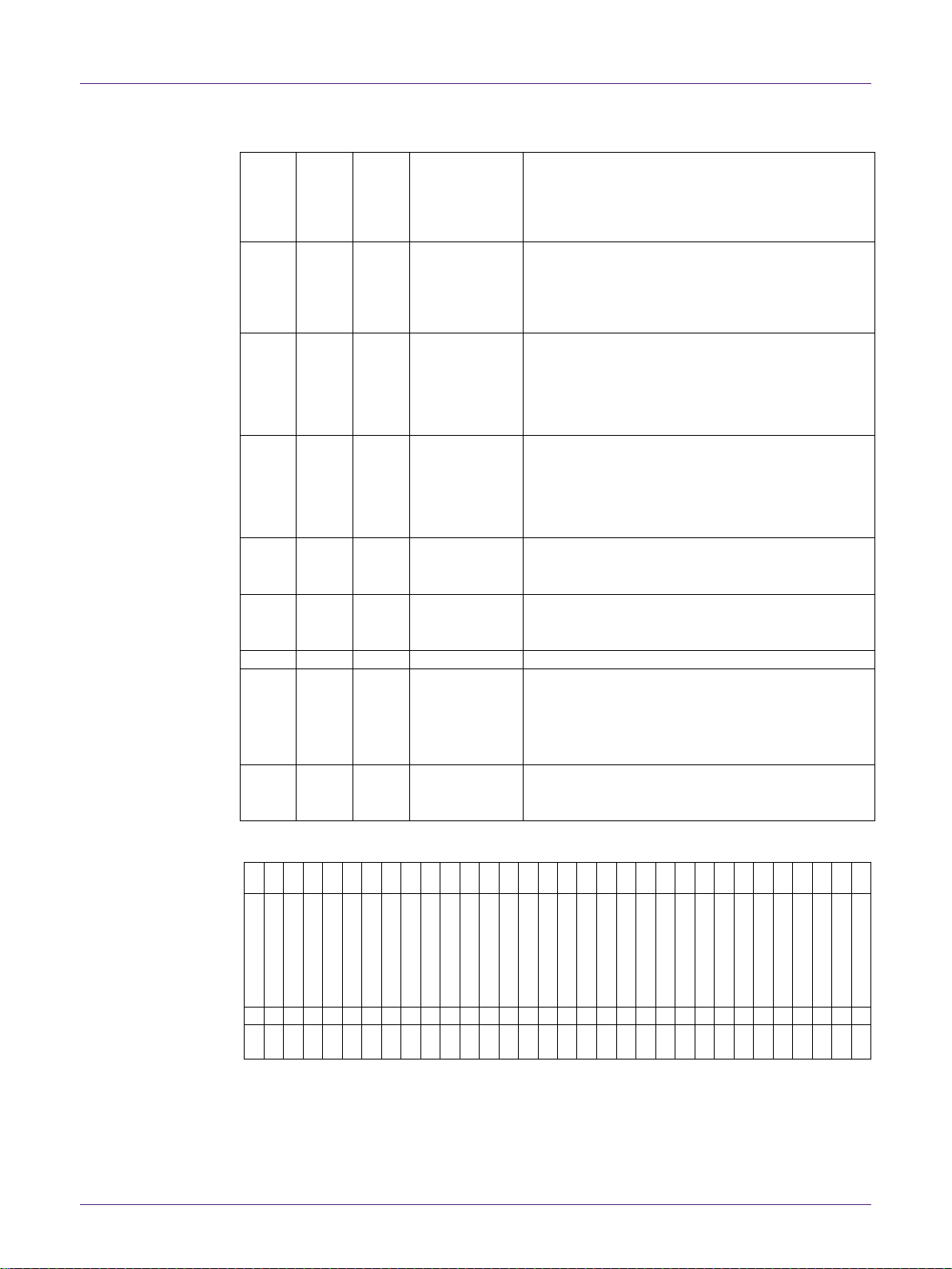
NXP Semiconductors
QN902x
User Manual of QN902x
UM10996
All information provided in this document is subject to legal disclaimers.
© NXP Semiconductors N.V. 2018. All rights reserved.
User Manual
Rev 1.3 — 05 November 2018
42 of 128
13-12
RW
10b
BUF_BM_GAIN[
1-0]
PGA bias current
00b = 50%
01b = 75%
10b = 100%
11b = 200%
11-10
RW
01b
BUF_IN_P[1-0]
ADC buffer positive input
00b = Not Used
01b = VCM
10b = Input from the selected ADC channel
11b = Ground
9-8
RW
01b
BUF_IN_N[1-0]
ADC buffer negative input
00b = Not Used
01b = VCM
10b = Input from the selected ADC channel
11b = Ground
7-6
RW
00b
RES_SEL[1-0]
ADC resolution
00b = RSVD
01b = 10bit
10b = 8bbit
11b = RSVD
5
RW
0
WCMP_SEL
Window compare data input
0 = ADC result
1 = Decimation result
4
RW
0
WCMP_EN
Enable of window compare
0 = Disable
1 = Enable
3
RW
0
RSVD
Reserved.
2-1
RW
00b
DECI_DIV[1-0]
ADC decimation rate
00b = 64
01b = 256
10 b =1024
11b = RSVD
0
RW
0
DECI_EN
Enable of decimation
0 = Disable
1 = Enable
Table 30 ADC2
31
30
29
28
27
26
25
24
23
22
21
20
19
18
17
16
15
14
13
12
11
10
9 8 7 6 5 4 3 2 1
0
WCMP_TH_HI[15] WCMP_TH_HI[14] WCMP_TH_HI[13] WCMP_TH_HI[12] WCMP_TH_HI[11] WCMP_TH_HI[10]
WCMP_TH_HI[9] WCMP_TH_HI[8] WCMP_TH_HI[7] WCMP_TH_HI[6] WCMP_TH_HI[5] WCMP_TH_HI[4] WCMP_TH_HI[3] WCMP_TH_HI[2] WCMP_TH_HI[1] WCMP_TH_HI[0]
WCMP_TH_LO[15] WCMP_TH_LO[14] WCMP_TH_LO[13] WCMP_TH_LO[12] WCMP_TH_LO[11] WCMP_TH_LO[10]
WCMP_TH_LO[9] WCMP_TH_LO[8] WCMP_TH_LO[7] WCMP_TH_LO[6] WCMP_TH_LO[5] WCMP_TH_LO[4] WCMP_TH_LO[3] WCMP_TH_LO[2] WCMP_TH_LO[1] WCMP_TH_LO[0]
0
1 1 1 1 1 1 1 1 1 1 1 1 1
1
1 1 0 0 0 0 0 0 0 0 0 0 0 0 0 0 0
RW
RW
RW
RW
RW
RW
RW
RW
RW
RW
RW
RW
RW
RW
RW
RW
RW
RW
RW
RW
RW
RW
RW
RW
RW
RW
RW
RW
RW
RW
RW
RW
Page 43

NXP Semiconductors
QN902x
User Manual of QN902x
UM10996
All information provided in this document is subject to legal disclaimers.
© NXP Semiconductors N.V. 2018. All rights reserved.
User Manual
Rev 1.3 — 05 November 2018
43 of 128
Bit
Type
Reset
Symbol
Description
31-16
RW
7FFFh
WCMP_TH_HI[15-0]
Windows compare high threshold
If ADC result is larger than WCMP_TH_HI, one
interrupt will be generated.
15-0
RW
8000h
WCMP_TH_LO[15-0]
Windows compare low threshold.
If ADC result is smaller than WCMP_TH_LO, one
interrupt will be generated.
Table 31 SR
31
30
29
28
27
26
25
24
23
22
21
20
19
18
17
16
15
14
13
12
11
10
9 8 7 6 5 4 3 2 1
0
RSVD
RSVD
RSVD
RSVD
RSVD
RSVD
RSVD
RSVD
RSVD
RSVD
RSVD
RSVD
RSVD
RSVD
RSVD
RSVD
RSVD
RSVD
RSVD
RSVD
RSVD
RSVD
RSVD
RSVD
RSVD
RSVD
RSVD
RSVD
RSVD
FIFO_OF_IF
WCMP_IF_IF
DAT_RDY_IF
0 0 0 0 0 0 0 0 0 0 0 0 0 0 0 0 0 0 0 0 0 0 0 0 0 0 0 0 0 0 0
0
R R R R R R R R R R R R R R R R R R R R R R R R R R R R R
RW1
RW1
R
Bit
Type
Reset
Symbol
Description
31-3
RW
0
RSVD
Reserved
2
RW1
0
FIFO_OF_IF
FIFO overflow interrupt flag, write 1 to clear
1
RW1
0
WCMP_IF_IF
Window compare interrupt flag, write 1 to clear
0 R 0
DAT_RDY_IF
Data ready interrupt flag, to be cleared automatically after
FIFO data is read.
Table 32 DATA
31
30
29
28
27
26
25
24
23
22
21
20
19
18
17
16
15
14
13
12
11
10
9 8 7 6 5 4 3 2 1
0
RSVD
RSVD
RSVD
RSVD
RSVD
RSVD
RSVD
RSVD
RSVD
RSVD
RSVD
RSVD
RSVD
RSVD
RSVD
RSVD
ADC_DATA[15] ADC_DATA[14]
ADC_DATA[13] ADC_DATA[12] ADC_DATA[11]
ADC_DATA10]
ADC_DATA[9] ADC_DATA[8] ADC_DATA[7] ADC_DATA[6] ADC_DATA[5] ADC_DATA[4] ADC_DATA[3] ADC_DATA[2] ADC_DATA[1] ADC_DATA[0]
0 0 0 0 0 0 0 0 0 0 0 0 0 0 0 0 0 0 0 0 0 0 0 0 0 0 0 0 0 0 0
0
R R R R R R R R R R R R R R R R R R R R R R R R R R R R R R R
R
Bit
Type
Reset
Symbol
Description
31-16 R 0
RSVD
Reserved
15-0 R 0
ADC_DATA[15-0]
ADC data read from FIFO, in 2’s-complement
4.4 Software Document and Example Code
Refer to “QN902X API Programming Guide v1.0.pdf” and ADC example source code in
the SDK.
Page 44

NXP Semiconductors
QN902x
User Manual of QN902x
UM10996
All information provided in this document is subject to legal disclaimers.
© NXP Semiconductors N.V. 2018. All rights reserved.
User Manual
Rev 1.3 — 05 November 2018
44 of 128
Page 45

NXP Semiconductors
QN902x
User Manual of QN902x
UM10996
All information provided in this document is subject to legal disclaimers.
© NXP Semiconductors N.V. 2018. All rights reserved.
User Manual
Rev 1.3 — 05 November 2018
45 of 128
5. Comparator
There are two Analog Comparators integrated in QN902x, which supports many
features and are easily configured to use.
5.1 Features
The main features of Analog Comparator are as follows:
Input pins multiplexed with I/O pins
Input pins enabled/disabled independently
Selectable inputs on negative input pin
Selectable internal reference voltage level
Support hysteresis control function
Support configurable interrupt polarity
Output routed to multiple peripherals: Timer, INT Controller, Wakeup
Source
Page 46

NXP Semiconductors
QN902x
User Manual of QN902x
UM10996
All information provided in this document is subject to legal disclaimers.
© NXP Semiconductors N.V. 2018. All rights reserved.
User Manual
Rev 1.3 — 05 November 2018
46 of 128
5.2 Function Description
A block diagram of the comparator module is illustrated in figure below.
5.3 Comparator Operation
5.3.1 Comparator Inputs
Depending on the comparator operating mode, the input to the comparator
negative pin may be from the input pin or an internal configurable voltage
references. The input to the comparator positive pin is fixed to be from the
input pin.
Note: VREF is internally connected
Comparator 0
Comparator 1
Notes:
1. VREF is internally connected, range selectable from VDD1 /16 to VDD15/16
2. Input pins of ACMP1 share pins with SWD. SWD function has to be disabled if
ACMP1 enabled.
Page 47

NXP Semiconductors
QN902x
User Manual of QN902x
UM10996
All information provided in this document is subject to legal disclaimers.
© NXP Semiconductors N.V. 2018. All rights reserved.
User Manual
Rev 1.3 — 05 November 2018
47 of 128
The input pins to the comparator are multiplexed with I/O pins, must be
enabled as analog input by control bit AINx_EN before using it as comparator
input.
5.3.2 Comparator Outputs
The output of comparator are routed to three peripherals: Timer, Interrupt
Controller, Wakeup Source Controller.
When timer working in Capture mode, the comparator output can be used to
trigger the Timer capture operation. The ICSS bit of Timer TCR register is used
to enable the input to Timer. Once enabled, the output of Comparator 0 is
connected with Timer0 and Timer 2, while output of Comparator 1 is
connected with Timer 1 and Timer 3.
5.3.3 Comparator Configuration
The comparator module provides a flexible configuration to allow the module to
be tailored to the needs of an application. The QN902x Comparator module has
individual control over the enable, output polarity, hysteresis and negative
input selection. The negative input can be selected in a variety of voltage level
when configured as using internal reference.
5.4 Register Description
The Analog Comparator Control register base address is 0x400000b8.
5.4.1 Register Description
ANALOG_CTRL
Description of Word
Bit
Type
Reset
Name
Description
31-28
RW
0000b
ACMP0[3-0]
Comparator 0 reference voltage selection 0000b =
Select external reference voltage
0001b = Select internal reference voltage (1/16
VDD)
0010b = Select internal reference voltage (2/16
VDD)
0011b = Select internal reference voltage (3/16
VDD)
31
30
29
28
27
26
25
24
23
22
21
20
19
18
17
16
15
14
13
12
11
10
9 8 7 6 5 4 3 2 1
0
ACMP0[3] ACMP0[2] ACMP0[1] ACMP0[0] ACMP1[3] ACMP1[2] ACMP1[1] ACMP1[0] BD[1]
BD[0]
EN_ACMP0 EN_ACMP1 EN_BT
EN_BD
EN_TS
ACMP1_VALUE ACMP0_VALUE ACMP1_HYST ACMP2_HYST AIN3_EN AIN2_EN AIN1_EN AIN0_EN BUCK_PMDR BUCK_NMDR PA_GAIN[4] XSP_CSEL SLEEP_TRIG NC[3-0]
0 0 0 0 0 0 0 0 0 0 0 0 0 0 0 0 0 0 0 0 0 0 0 0 0 0 0 0 1 1 1
1
RW
RW
RW
RW
RW
RW
RW
RW
RW
RW
RW
RW
RW
RW
RW
RW
RW
RW
RW
RW
RW
RW
RW
RW
RW
RW
RW
RW
RW
RW
RW
RW
Page 48

NXP Semiconductors
QN902x
User Manual of QN902x
UM10996
All information provided in this document is subject to legal disclaimers.
© NXP Semiconductors N.V. 2018. All rights reserved.
User Manual
Rev 1.3 — 05 November 2018
48 of 128
0100b = Select internal reference voltage (4/16
VDD)
0101b = Select internal reference voltage (5/16
VDD)
0110b = Select internal reference voltage (6/16
VDD)
0111b = Select internal reference voltage (7/16
VDD)
1000b = Select internal reference voltage (8/16
VDD)
1001b = Select internal reference voltage (9/16
VDD)
1010b = Select internal reference voltage (10/16
VDD)
1011b = Select internal reference voltage (11/16
VDD)
1100b = Select internal reference voltage (12/16
VDD)
1101b = Select internal reference voltage (13/16
VDD)
1110b = Select internal reference voltage (14/16
VDD)
1111b = Select internal reference voltage (15/16
VDD)
27-24
RW
0000b
ACMP1[3-0]
Comparator 1 reference voltage selection
0000b = Select external reference voltage
0001b = Select internal reference voltage (1/16
VDD)
0010b = Select internal reference voltage (2/16
VDD)
0011b = Select internal reference voltage (3/16
VDD)
0100b = Select internal reference voltage (4/16
VDD)
0101b = Select internal reference voltage (5/16
VDD)
0110b = Select internal reference voltage (6/16
VDD)
0111b = Select internal reference voltage (7/16
VDD)
1000b = Select internal reference voltage (8/16
VDD)
1001b = Select internal reference voltage (9/16
VDD)
1010b = Select internal reference voltage (10/16
VDD)
1011b = Select internal reference voltage (11/16
VDD)
1100b = Select internal reference voltage (12/16
VDD)
1101b = Select internal reference voltage (13/16
VDD)
1110b = Select internal reference voltage (14/16
VDD)
Page 49

NXP Semiconductors
QN902x
User Manual of QN902x
UM10996
All information provided in this document is subject to legal disclaimers.
© NXP Semiconductors N.V. 2018. All rights reserved.
User Manual
Rev 1.3 — 05 November 2018
49 of 128
1111b = Select internal reference voltage (15/16
VDD)
23-22
RW
00b
BD[1-0]
Browned out detector threshold voltage selection
00b = 1.76V
01b = 1.7V
10b = 1.65V
11b = 1.6V
21
RW
0
EN_ACMP0
1 is Enable comparator 0
20
RW
0
EN_ACMP1
1 is Enable comparator 1
19
RW
0
EN_BT
1 is Enable battery monitor
18
RW
0
EN_BD
1 is Enable browned out detector
17
RW
0
Reserved
Reserved
16
RW 0 ACMP1_VALUE
0 = When ACMP1 is 1, generate interrupt;
1 = When ACMP1 is 0, generate interrupt;
15
RW 0 ACMP0_VALUE
0 = When ACMP0 is 1, generate interrupt;
1 = When ACMP0 is 0, generate interrupt;
14
RW 0 ACMP0_HYST
1 is Enable hysteresis of analog comparator 0
13
RW 0 ACMP1_HYSR
1 is Enable hysteresis of analog comparator 1
12-9
RW 0 AINx_EN
1 is Enable P0_7/6 and P3_1/0 as Analog input
ONLY.
8
RW 0 BUCK_PMDR
7
RW 0 BUCK_NMDR
6
RW 0 PA_GAIN[4]
Together with PA_GAIN[0-3], PA_GAIN[0-4]
means:
11111---------- 4dBm
01111---------- 3dBm
11110---------- 2dBm
01110---------- 1dBm
01101---------- 0dBm
01100---------- -2dBm
01010---------- -4dBm
01001---------- -6dBm
01000---------- -8dBm
00110---------- -10dBm
00101---------- -12dBm
00100---------- -14dBm
00010---------- -16dBm
00001---------- -18dBm
00000---------- -20dBm
5
RW 0 XSP_CSEL
Select the load capacitor in speed up mode. All of
the load cap is removed in speed up mode when
XSP_SEL=1.
4
RW 0 SLEEP_TRIG
When it is 1, sleep counter registers of BLE can be
reloaded during BLE deep sleep state.
3-0
RW
1111b
NC[3-0]
No connected;
Page 50

NXP Semiconductors
QN902x
User Manual of QN902x
UM10996
All information provided in this document is subject to legal disclaimers.
© NXP Semiconductors N.V. 2018. All rights reserved.
User Manual
Rev 1.3 — 05 November 2018
50 of 128
6. Clock Management Unit (CMU)
The Clock Management unit (CMU) is responsible for controlling oscillators and clocks.
The CMU provides the capability to selectably turn on and off the clocks to peripherals
in addition to enabling/disabling and configuring of all available oscillators. The high
degree of flexibility enables software to minimize the energy consumption in any
specific application by not wasting power on the peripherals and the oscillators that are
inactive.
6.1 Clock generation
Figure 7 shows the block diagram of the Clock unit.
Page 51

NXP Semiconductors
QN902x
User Manual of QN902x
UM10996
All information provided in this document is subject to legal disclaimers.
© NXP Semiconductors N.V. 2018. All rights reserved.
User Manual
Rev 1.3 — 05 November 2018
51 of 128
Ref PLL
SPI 0
Clcok
SPI 1
Clcok
UART 0
Clcok
UART 1
Clcok
BLE
Clock
Timer0
Clock
Timer1
Clock
Timer2
Clock
Timer3
Clcok
32 kHz crystal
oscillator
32 kHz RC
oscillator
SEL_CLK_32K
32/16MHz crystal
oscillator
20MHz RC
oscillator
XDIV
CLK_MUX
(system clock select)
FCLK
AHB_
DIVIDER
DMA HCLK
GPIO
Clcok
AHB Clock
SYS_CLK
AHB_DIV
_BYPASS
32KHz
sleep timer
RTC
Clock
32MHz
PLL Clcok
ADC
Clock
ADC_CLK_SEL
ADC_DIV_BYPASS
USART1_DIV_BYPASS
USART0_DIV_BYPASS
PCLK
APB_DIV_BYPASS
TIMER_DIV
_BYPASS
XTAL1_32K
XTAL2_32K
X32INJ
(Select external
32kHz clock)
XINJ
(Select 32/16MHz
crystal oscillator)
XTAL1
XTAL2
APB Clock
SPI_AHB
Clock
BLE_AHB
Clock
PWM
Clock
BLE_DIV_BYPASS
CPU HCLK
Peripheral
CLK_OUT_SEL[1]
CLK_OUT_SEL[0]
CLKOUT1
CLKOUT0
ADC_DIV
(ADC divider)
Clock
Gating
Clock
Gating
Clock
Gating
Clock
Gating
Clock
Gating
Clock
Gating
APB_DIVIDER
Clock
Gating
BLE_DIVIDER
USART1_DIVDER
USART1_DIVDER
TIMER_DIVDER
Clock
Gating
Clock
Gating
Clock
Gating
Clock
Gating
Clock
Gating
Clock
Gating
Clock
Gating
Clock
Gating
Figure 7 Clock block diagram
6.2 Clock sources
The QN902X CMU uses following clock sources:
· 32/16 MHz crystal oscillator.
· 20 MHz RC oscillator.
Page 52

NXP Semiconductors
QN902x
User Manual of QN902x
UM10996
All information provided in this document is subject to legal disclaimers.
© NXP Semiconductors N.V. 2018. All rights reserved.
User Manual
Rev 1.3 — 05 November 2018
52 of 128
· 32.768 KHz oscillator
· 32.768 KHz crystal oscillator
· 32 KHz RC oscillator.
· 32 MHz PLL clock output for system
By default, the 20MHz internal RC oscillator is enabled and selected.
In the deep sleep mode, all clock sources can be disabled. In the other modes, at least
one clock source must be enabled.
6.3 Clock description
The system clock is selected from four clock sources by configuring the CLK_MUX
register, and it generates all clocks for the chip, except the low frequency 32 kHz clock
for the RTC and the sleep timer. The ADC clock can be selected among the 32 kHz clock
and the system clock. The maximum system clock frequency is 32MHz.
The AHB clock is derived from the system clock and supplies all the clocks in the
peripherals, except the ADC, the RTC and 32 kHz sleep timer blocks. The APB clock is
derived from the AHB clock and is used for the registers.
6.4 Pin description
Table 33 shows pins that are associated with the clock block functions.
Table 33 Pin summary
Pin name
Type
Direc
tion
Description
CLOCKOUT1
Digital
O
Clockout1 pin, connected to P0_3 or P3_3 by configuring
PIN_MUX_CTRL
CLOCKOUT0
Digital
O
Clockout0 pin, connected to P0_4 or P1_3 by configuring
PIN_MUX_CTRL
XTAL1_32K
Analog O
Connected to 32.768 kHz crystal. Unconnected if RCOSC used.
XTAL2_32K
Analog I
Connected to 32.768 kHz crystal or external 32k clock. Unconnected
if RC OSC used.
XTAL1
Analog O
Connected to 16 MHz or 32 MHz crystal.
XTAL2
Analog I
Connected to 16 MHz or 32 MHz crystal.
6.5 Basic configuration
Each clock gating can disable or enable the clock independently by setting
CLK_RST_SOFT_CLK or clearing CLK_RST_SOFT_SET. The user can disable peripheral by
disabling the corresponding clock.
The dividers can be configured independently, therefore, all clocks can run at different
frequencies.
6.5.1 System clock and AHB clock configuration
The system clock can be sourced from the internal 20 MHz oscillator, from the 32MHz
Page 53

NXP Semiconductors
QN902x
User Manual of QN902x
UM10996
All information provided in this document is subject to legal disclaimers.
© NXP Semiconductors N.V. 2018. All rights reserved.
User Manual
Rev 1.3 — 05 November 2018
53 of 128
PLL, directly from the 16/32 MHz external oscillator, or from 32 kHz (32.768 kHz)
oscillator
The AHB clock is derived from the system clock and serves as a clock source for CPU
HCLK, FCLK, SPI_AHB, GPIO, BLE_AHB and DMA.
The CPU HCLK and FCLK are the clock sources of the core. The SPI_AHB clocks the
internal flash. The BLE_AHB is used for the BLE block and does not need to be
configured. All clocks, except the CPU HCLK and FCLK, can be disabled when
corresponding block is not active.
6.5.2 Configure APB clock
The APB clock is derived from the AHB clock and serves as the clock source for all
registers. Due to the divider, the APB clock is lower than or equal to the core clock.
Because all peripheral registers are clocked by the APB clock, the APB clock should not
be configured slower than the peripheral clocks.
6.5.3 Configure BLE clock
The BLE_AHB is clocked by the AHB clock, and the BLE clock is derived from the AHB
clock. They are used for BLE RF block and usually do not need to be configured by the
user. The BLE clock can only run at 8 or 16 MHz
Note: BLE RF block requires correct configuration of the BLE_AHB and BLE clocks.
Therefore, it is recommended to use the Software Development Kit.
6.5.4 Configure peripheral clocks
The peripheral clocks are derived from the AHB clock. The dividers of all peripheral
blocks clock can be configured independently, therefore, all peripheral clocks can run at
different frequencies.
Every peripheral block can be disabled to reduce the power by disabling/enabling the
corresponding clock independently.
6.6 Register description
The System Registers are based on 0x40000000.
6.6.1 System Clock Register Description
Table 34 System Clock Register
Offset
Name
Description
000h
CRSS
Enable clock gating and set block reset
004h
CRSC
Disable clock gating and clear block reset
008h
CMDCR
Set clock switch and clock divider
00Ch
STCR
Set systick timer STCALIB and STCLKEN
6.6.1.1 CRSS
CRSS is Enable clock gating and set block reset register, address is 0x40000000
Page 54

NXP Semiconductors
QN902x
User Manual of QN902x
UM10996
All information provided in this document is subject to legal disclaimers.
© NXP Semiconductors N.V. 2018. All rights reserved.
User Manual
Rev 1.3 — 05 November 2018
54 of 128
31
30
29
28
27
26
25
24
23
22
21
20
19
18
17
16
15
14
13
12
11
10
9 8 7 6 5 4 3 2 1
0
GATING_TIMER3 GATING_TIMER2 GATING_TIMER1 GATING_TIMER0
GATING_UART1 GATING_UART0
GATING_SPI1 GATING_SPI0
GATING_32K_CLK
GATING_SPI_AHB
GATING_GPIO
GATING_ADC
GATING_DMA
GATING_BLE_AHB
GATING_PWM
REBOOT_SYS
LOCKUP_RST
BLE_RST
DP_RST
DPREG_RST
RTC_RST
I2C_RST
GPIO_RST
WDOG_RST
TIMER3_RST TIMER2_RST TIMER1_RST TIMER0_RST
USART1_RST USART0_RST
DMA_RST
CPU_RST
0 0 0 1 1 1 1 1 1 1 1 1 1 1 1 0 0 1 1 1 1 1 1 1 1 1 1 1 1 1 1
1
RW1
RW1
RW1
RW1
RW1
RW1
RW1
RW1
RW1
RW1
RW1
RW1
RW1
RW1
RW1
RW1
RW1
RW1
RW1
RW1
RW1
RW1
RW1
RW1
RW1
RW1
RW1
RW1
RW1
RW1
RW1
RW1
Description of Word
Bit
Type
Reset
Symbol
Description
31
RW1
0
GATING_TIMER3
Write 1 to disable timer 3 clock
30
RW1
0
GATING_TIMER2
Write 1 to disable timer 2 clock
29
RW1
0
GATING_TIMER1
Write 1 to disable timer 1 clock
28
RW1
1
GATING_TIMER0
Write 1 to disable timer 0 clock
27
RW1
1
GATING_UART1
Write 1 to disable UART 1 clock
26
RW1
1
GATING_UART0
Write 1 to disable UART 0 clock
25
RW1
1
GATING_SPI1
Write 1 to disable SPI 1 clock
24
RW1
1
GATING_SPI0
Write 1 to disable SPI 0 clock
23
RW1
1
GATING_32K_CLK
Write 1 to disable 32KHz clock
22
RW1
1
GATING_SPI_AHB
Write 1 to disable FLASH control clock
21
RW1
1
GATING_GPIO
Write 1 to disable GPIO clock
20
RW1
1
GATING_ADC
Write 1 to disable ADC clock
19
RW1
1
GATING_DMA
Write 1 to disable DMA clock
18
RW1
1
GATING_BLE_AHB
Write 1 to disable BLE AHB clock
17
RW1
1
GATING_PWM
Write 1 to disable PWM clock
16
RW1
0
REBOOT_SYS
Write 1 to reboot entire system
15
RW1
0
LOCKUP_RST
Write 1 to enable LOCKUP reset control
14
RW1
1
BLE_RST
Write 1 to set BLE reset
13
RW1
1
DP_RST
Write 1 to set datapath reset
12
RW1
1
DPREG_RST
Write 1 to set datapath register reset
11
RW1
1
RTC_RST
Write 1 to set sleep timer reset
Page 55

NXP Semiconductors
QN902x
User Manual of QN902x
UM10996
All information provided in this document is subject to legal disclaimers.
© NXP Semiconductors N.V. 2018. All rights reserved.
User Manual
Rev 1.3 — 05 November 2018
55 of 128
10
RW1
1
I2C_RST
Write 1 to set I2C reset
9
RW1
1
GPIO_RST
Write 1 to set GPIO reset
8
RW1
1
WDOG_RST
Write 1 to set Watch Dog reset
7
RW1
1
TIMER3_RST
Write 1 to set timer 3 reset
6
RW1
1
TIMER2_RST
Write 1 to set timer 2 reset
5
RW1
1
TIMER1_RST
Write 1 to set timer 1 reset
4
RW1
1
TIMER0_RST
Write 1 to set timer 0 reset
3
RW1
1
USART1_RST
Write 1 to set USART1 (SPI 1 and UART 1) reset
2
RW1
1
USART0_RST
Write 1 to set USART0 (SPI 0 and UART 0) reset
1
RW1
1
DMA_RST
Write 1 to set DMA reset
0
RW1
1
CPU_RST
Write 1 to set CPU reset
6.6.1.2 CRSC
CRSC is Disable clock gating and clear block reset register, the address is 0x40000004
31
30
29
28
27
26
25
24
23
22
21
20
19
18
17
16
15
14
13
12
11
10
9 8 7 6 5 4 3 2 1
0
NGATING_
TIMER_3
NGATING_TIMER_2 NGATING_TIMER_1 NGATING_TIMER_0
NGATING_UART_1 NGATING_UART_0
NGATING_SPI_1 NGATING_SPI_0
NGATING_32K_CLK
NGATING_SPI_AHB
NGATING_GPIO
NGATING_ADC
NGATING_DMA
NGATING_BLE_AHB
NGATING_PWM
RSVD
DIS_LCOKUP_RST
CLR_BLE_RST
CLR_DP_RST
CLR_DPREG_RST
CLR_SLPTIM_RST
CLR_I2C_RST
CLR_GPIO_RST
CLR_WDOG_RST
CLR_TIMER3_RST CLR_TIMER2_RST CLR_TIMER1_RST CLR_TIMER0_RST
CLR_USART1_RST CLR_USART0_RST
CLR_DMA_RST
CLR_CPU_RST
X x x x x x x x x x x x x x x x x x x X x x x x x x x x x x x
x
W1
W1
W1
W1
W1
W1
W1
W1
W1
W1
W1
W1
W1
W1
W1 R W1
W1
W1
W1
W1
W1
W1
W1
W1
W1
W1
W1
W1
W1
W1
W1
Description of Word
Bit
Type
Reset
Symbol
Description
31
W1 x NGATING_TIMER_3
Write 1 to enable timer 3 clock
30
W1 x NGATING_TIMER_2
Write 1 to enable timer 2 clock
29
W1 x NGATING_TIMER_1
Write 1 to enable timer 1 clock
28
W1 x NGATING_TIMER_0
Write 1 to enable timer 0 clock
27
W1 x NGATING_UART_1
Write 1 to enable UART 1 clock
26
W1 x NGATING_UART_0
Write 1 to enable UART 0 clock
25
W1 x NGATING_SPI_1
Write 1 to enable SPI 1 clock
Page 56

NXP Semiconductors
QN902x
User Manual of QN902x
UM10996
All information provided in this document is subject to legal disclaimers.
© NXP Semiconductors N.V. 2018. All rights reserved.
User Manual
Rev 1.3 — 05 November 2018
56 of 128
24
W1 x NGATING_SPI_0
Write 1 to enable SPI 0 clock
23
W1 x NGATING_32K_CLK
Write 1 to enable 32KHz clock
22
W1 x NGATING_SPI_AHB
Write 1 to enable SPI AHB clock
21
W1 x NGATING_GPIO
Write 1 to enable GPIO clock
20
W1 x NGATING_ADC
Write 1 to enable ADC clock
19
W1 x NGATING_DMA
Write 1 to enable DMA clock
18
W1 x NGATING_BLE_AHB
Write 1 to enable BLE AHB clock
17
W1 x NGATING_PWM
Write 1 to enable PWM clock
16 R x
RSVD
Reserved
15
W1 x DIS_LOCKUP_RST
Write 1 to disable LOCKUP reset control
14
W1 x CLR_BLE_RST
Write 1 to clear BLE reset
13
W1 x CLR_DP_RST
Write 1 to clear datapath reset
12
W1 x CLR_DPREG_RST
Write 1 to clear datapath register reset
11
W1 x CLR_SLPTIM_RST
Write 1 to clear sleep timer reset
10
W1 x CLR_I2C_RST
Write 1 to clear I2C reset
9
W1 x CLR_GPIO_RST
Write 1 to clear GPIO reset
8
W1 x CLR_WDOG_RST
Write 1 to clear Watch Dog reset
7
W1 x CLR_TIMER3_RST
Write 1 to clear timer 3 reset
6
W1 x CLR_TIMER2_RST
Write 1 to clear timer 2 reset
5
W1 x CLR_TIMER1_RST
Write 1 to clear timer 1 reset
4
W1 x CLR_TIMER0_RST
Write 1 to clear timer 0 reset
3
W1 x CLR_USART1_RST
Write 1 to clear USART1 (SPI 1 and UART 1) reset
2
W1 x CLR_USART0_RST
Write 1 to clear USART0 (SPI 0 and UART 0) reset
1
W1 x CLR_DMA_RST
Write 1 to clear DMA reset
0
W1 x CLR _CPU_RST
Write 1 to clear CPU reset
6.6.1.3 CMDCR
CMDCR is set clock switch and clock divider register, address is 0x40000008
31
30
29
28
27
26
25
24
23
22
21
20
19
18
17
16
15
14
13
12
11
10
9 8 7 6 5 4 3 2 1
0
Page 57

NXP Semiconductors
QN902x
User Manual of QN902x
UM10996
All information provided in this document is subject to legal disclaimers.
© NXP Semiconductors N.V. 2018. All rights reserved.
User Manual
Rev 1.3 — 05 November 2018
57 of 128
CLK_MUX[1] CLK_MUX[0]
SEL_CLK_32K
BLE_FRQ_SEL
BLE_DIV_BYPASS
BLE_DIVIDER
AHB_DIV_BYPASS
AHB_DIVIDER[8] AHB_DIVIDER[7] AHB_DIVIDER[6] AHB_DIVIDER[5] AHB_DIVIDER[4] AHB_DIVIDER[3] AHB_DIVIDER[2] AHB_DIVIDER[1] AHB_DIVIDER[0]
USART1_DIV_BYPASS
USART1_DIV
IDER[2]
USART1_DIVIDER[1] USART1_DIVIDER[0]
USART0_DIV_BYPASS
USART0_DIVIDER[2] USART0_DIVIDER[1] USART0_DIVIDER[0]
RSVD
APB_DIV_BYPASS
APB_DIVIDER[1] APB_DIVIDER[0]
TIMER_DIV_BYPASS
TIMER_DIVIDER[2] TIMER_DIVIDER[1] TIMER_DIVIDER[0]
0 1 0 1 1 0 1 0 0 0 0 0 0 0 0 0 0 0 0 1 1 0 0 0 0 0 0 1 0 0 0
1
RW
RW
RW
RW
RW
RW
RW
RW
RW
RW
RW
RW
RW
RW
RW
RW
RW
RW
RW
RW
RW
RW
RW
RW
RW
RW
RW
RW
RW
RW
RW
RW
Description of Word
Bit
Type
Reset
Symbol
Description
31-30
RW
01b
CLK_MUX[1-0]
Select system clock source.
00b = High frequency crystal 16MHz or
32MHz;
01b = 20MHz internal high frequency;
10b = 32MHz PLL output;
11b = 32KHz low speed clock;
29
RW
0
SEL_CLK_32K
1 = Select 32KHz clock from RCO
0 = Select 32KHz clock from XTAL32
28
RW
1
BLE_FRQ_SEL
Describe BLE clock frequency.
0 = 8 MHz;
1 = 16 MHz
27
RW
1
BLE_DIV_BYPASS
‘1’ is bypass BLE Divider; Only 16 or 8 MHz are
supported;
26
RW
0
BLE_DIVIDER
If BLE_DIV_BYPASS is ‘0’,
BLE_CLK = AHB_CLK / (2*(BLE_DIVIDER +1));
Only 16 or 8 MHz are supported;
25
RW
1
AHB_DIV_BYPASS
‘1’ is bypass AHB Divider;
24-16
RW
0
AHB_DIVIDER[8-0]
If AHB_DIV_BYPASS is ‘0’,
AHB_CLK = SYS_CLK/(2*(APB_DIVIDER+1));
15
RW
0
USART1_DIV_BYPASS
‘1’ is bypass USART1 Divider;
14-12
RW
001b
USART1_DIVIDER[2-0]
If USART1_DIV_BYPASS is ‘0’,
USART1_CLK =
AHB_CLK/(2*(USART1_DIVIDER+1))
11
RW
1
USART0_DIV_BYPASS
‘1’ is bypass USART0 Divider;
10-8
RW
0
USART0_DIVIDER[2-0]
If USART0_DIV_BYPASS is ‘0’,
USART0_CLK =
AHB_CLK/(2*(USART1_DIVIDER+1))
7
RW
0
RSVD
Reserved
6
RW
0
APB_DIV_BYPASS
‘1’ is bypass APB Divider;
5-4
RW
01b
APB_DIVIDER[1-0]
If APB_DIV_BYPASS is ‘0’,
Page 58

NXP Semiconductors
QN902x
User Manual of QN902x
UM10996
All information provided in this document is subject to legal disclaimers.
© NXP Semiconductors N.V. 2018. All rights reserved.
User Manual
Rev 1.3 — 05 November 2018
58 of 128
APB_CLK = AHB_CLK/(2*(APB_DIVIDER+1))
3
RW
0
TIMER_DIV_BYPASS
‘1’ is bypass TIMER Divider;
2-0
RW
001b
TIMER_DIVIDER[2-0]
If TIMER_DIV_BYPASS is ‘0’,
TIMER_CLK = AHB_CLK / (2*(TIMER_DIVIDER +
1));
6.6.1.4 STCR
STCR is set systick timer STCALIB and STCLKEN register, address is 0x4000000C. For
detailed description of the register, please refer to Table 6 STCR.
Page 59

NXP Semiconductors
QN902x
User Manual of QN902x
UM10996
All information provided in this document is subject to legal disclaimers.
© NXP Semiconductors N.V. 2018. All rights reserved.
User Manual
Rev 1.3 — 05 November 2018
59 of 128
7. Inter-Integrated Circuit (I2C) interface
The I2C (inter-integrated circuit) interface is a two-wire, bi-directional serial bus that can
be used to communicate with external devices using I2C protocol.
7.1 Features
Compliance with the I2C specification v2.1
Master or slave modes
Configurable master baud rate
Standard mode (up to 100 kbps)
Fast mode (up to 400 kbps)
7-bit addressing mode (10-bit address not supported)
Configurable device address in slave mode
SCL synchronization and bus arbitration in master mode
SCL stretching in slave mode
Master supports SCL synchronization and bus arbitration
8 bit shift register
7.2 Functional Description
The I2C-bus uses only two wires
SCL: serial clock line provided by the master device to synchronize the serial
data transfer
SDA: serial data/address line used to transmit and receive serial data.
When the I2C-bus is free, both the SDA and SCL lines should remain high. A High-to-Low
transition of the SDA line while SCL line remains high initiates a Start condition. A Low-toHigh transition of SDA line while SCL remains high initiates a Stop condition.
The data is always sent most-significant bit (MSB) first. Every byte should be immediately
followed by acknowledge (ACK) bit, which is sent by the receiver after last data byte.
Each bit is sampled during the high period of the SCL. Therefore, the SDA line may be
changed only during the low period of SCL and must be held stable during the high period
of SCL.
S or Sr
1 2 7 8 9 1 2 8 9
Slave Address (7-bit) R/W Data (8-bit)
START or
repeated START
condition
Acknowledgement
from slave
Acknowledgement
from receiver
ACK
Address match
interrupt within slave
ACK
Sr or P
START or
repeated START
condition
P
Sr
7.2.1 7-bit slave address
The first byte of data transferred by the master immediately after the START signal is the
Page 60

NXP Semiconductors
QN902x
User Manual of QN902x
UM10996
All information provided in this document is subject to legal disclaimers.
© NXP Semiconductors N.V. 2018. All rights reserved.
User Manual
Rev 1.3 — 05 November 2018
60 of 128
7-bit slave address and the read/write bit. In the master mode, the slave address should
be put into TXD to send. While in the slave mode, the slave address should be written
into SLAVE_ADDR[6:0], and the bus controller will monitor incoming slave address on the
SDA line to check if the address matches and this is the slave device to be addressed by
the master.
7.2.2 R/nW bit
The last bit following 7-bit slave address after START condition is the R/nW bit in the first
byte. The R/nW bit signal is sent by master device to set the data transfer direction. When
R/nW bit is 0, the I2C bus interface is in the write mode and the data transfer direction is
from master to slave. When R/nW bit is 1, the I2C bus interface is in the read mode and
the data transfer direction is from the slave to the master.
7.2.3 ACK/NACK
After completing the transfer of one-byte, the receiver should send an ACK bit to the
transmitter. The ACK pulse should occur during the 9th clock cycle of the SCL line. The
clock pulse required to transmit the ACK bit master should be generated by the master.
The transmitter should release the SDA line when the ACK clock pulse is received. The
receiver should also drive the SDA line low during the ACK clock pulse so that the SDA
keeps low during the high period of the ninth SCL pulse. The receiver will not drive the
SDA line low during ninth clock cycle if NACK is to be sent.
7.2.4 Data transfer
Once a successful slave addressing has been established, the data transfer can proceed
on a byte-by-byte basis in the direction specified by the R/nW bit sent by the master. Each
transferred byte is followed by an ACK bit on the 9th SCL clock cycle.
7.2.5 Stop or Repeated START signal
When the transfer ends, or is abnormal, the master will generate a STOP signal to abort
the data transfer or generate a Repeated START signal to start a new transfer cycle.
If the master, as the receiving device, does not acknowledge the slave device, the slave
device releases the SDA line for the master to generate a STOP or Repeated START signal.
7.2.6 SCL clock generation in master mode
The SCL is derived from PCLK, with a two-stage clock divider. The first one is a constant
divided by 20, and the second is divided by (SCL_RATIO + 1).
SCL = (PCLK/20)/(SCL_RATIO + 1)
7.3 Master Mode Operation
7.3.1 Master-transmit
The master initiates the data transfer with a START condition, followed by the Slave
Address and R/nW bit. If R/nW is low, the data transfer occurs from the master to the
slave. The ACK/NACK bit is sent by the slave. After the master receives the ACK/NACK bit,
Page 61

NXP Semiconductors
QN902x
User Manual of QN902x
UM10996
All information provided in this document is subject to legal disclaimers.
© NXP Semiconductors N.V. 2018. All rights reserved.
User Manual
Rev 1.3 — 05 November 2018
61 of 128
a TX_INT interrupt is generated to the processor to trigger the processing.
S Slave Address (7-bit) R/W A DATA (8-bit) A DATA (8-bit) A/A P
From master to slave
From slave to master
A = acknowledge (SDA LOW)
A = not acknowledge (SDA HIGH)
S = START condition
P = STOP condition
0=write
TX_INT TX_INT TX_INT
When the I2C controller (master mode) wants to send data to the slave, following steps
take place:
1. Read BUSY to see if the I2C bus is free. Wait until it is free.
2. Set MTSR_EN=1, and SCL_RATIO to the expected clock speed.
3. Write formatted slave address into TXD, and R/nW(=0) bit. Then write START bit to
initiate a transfer.
4. Wait for TX_INT interrupt, which is generated by the controller when ACK is received
from slave after master sent START condition, slave address and R/nW bit.
5. TX_INT interrupt processing: if ACK_RECV=0, write new data into TXD, and set
WR_EN. If ACK_RECV=1, stop the data transfer or re-start by setting STOP or START
bit. After the register is set, clear TX_INT interrupt, and controller will clock out the
waveform you have configured.
6. Repeat 5 and 6, if more data has to be sent.
7. Set STOP to send stop signal to finish the transfer.
7.3.2 Master-receive
If the master wants to read data from the slave, the R/nW should be high. After the data
byte is received, the master should send the ACK/NACK bit to the slave. The ACK/NACK
bit should be pre-programmed to ACK_SEND. Once the ACK is sent, a RX_INT signal is
generated to the processor to read the data and trigger further processing.
S Slave Address (7-bit) R/W A DATA A DATA A P
1=read
TX_INT RX_INT RX_INT
When the I2C controller (master mode) wants to read data from the slave, following steps
take place:
1. Read BUSY to see if the I2C bus is free. Wait until it is free.
2. Set MTSR_EN=1, and SCL_RATIO to the expected clock speed.
3. Write formatted slave address into TXD, and R/nW(=1) bit. Then write START bit to
initiate a transfer.
4. Wait for TX_INT interrupt, which is generated by the controller when ACK is received
from the slave after the master sent START condition, slave address and R/nW bit.
Page 62

NXP Semiconductors
QN902x
User Manual of QN902x
UM10996
All information provided in this document is subject to legal disclaimers.
© NXP Semiconductors N.V. 2018. All rights reserved.
User Manual
Rev 1.3 — 05 November 2018
62 of 128
8. TX_INT interrupt processing: if ACK_RECV=0, write RD_EN=1 to read data from the
slave and write ACK_SEND for the next read. If ACK_RECV=1, stop the data transfer
or re-start by configuring STOP bit or START bit. After the register is set, clear TX_INT
interrupt, and controller will clock out the waveform you configured.
5. If more data is to be read, set ACK_SEND to 0 in TXD and then set RD_EN=1, otherwise
set ACK_SEND to 1.
6. Set STOP to send stop signal to finish the transfer.
7.3.3 Slave-transmit
S Slave Address (7-bit) R/W A DATA A DATA A P
1=read
TX_INT TX_INT
Address match
interrupt within slave
When the I2C controller (slave mode) wants to send data to the master, following steps
take place:
1. Set SLV_EN=1, and SLAVE_ADDR[6:0].
2. If address match interrupt is detected and received R/nW=1, send ACK back to master
by configuring the ACK_SEND bit in TXD register
3. Write data into TXD to send. Then clear SAM_INT to clock out the ACK and TX data.
4. After slave sends the 8 bit data and receives ACK/NAK from master, TX interrupt
happens.
5. TX interrupt processing: if ACK_RECV is 0, write new data to TXD register, otherwise,
do wait the line is not busy.
6. Repeat step 4 again and again, until ACK_RECV is 1.
7. Data transfer finishes when STOP condition is detected.
7.3.4 Slave-receive
Address match
interrupt within slave
S Slave Address (7-bit) R/W A DATA (8-bit) A DATA (8-bit) A/A P
0=write
RX_INT RX_INT
When the I2C controller (slave mode) wants to receive data from the master, following
steps take place:
1. Set SLV_EN=1, and SLAVE_ADDR[6:0].
2. If address match interrupt is detected and received R/nW=0, send ACK back to the
master by configuring the ACK_SEND bit in TXD register
3. Wait for RX_INT, which indicates one byte has been received. Read the data and
send ACK back by configuring the ACK_SEND bit in TXD register, if more data is to
be received, otherwise, send NACK. All the transfer begins immediately after
Page 63
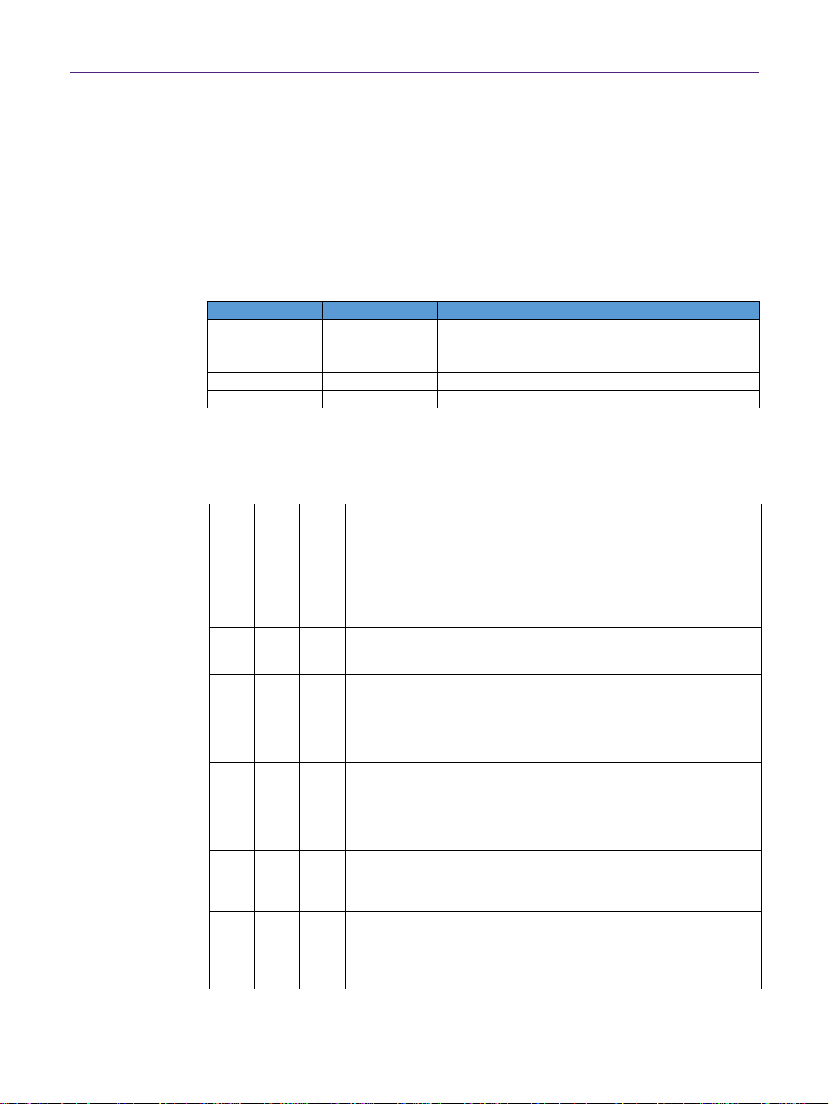
NXP Semiconductors
QN902x
User Manual of QN902x
UM10996
All information provided in this document is subject to legal disclaimers.
© NXP Semiconductors N.V. 2018. All rights reserved.
User Manual
Rev 1.3 — 05 November 2018
63 of 128
RX_INT interrupt is cleared.
4. Data transfer finishes when STOP condition is detected.
7.4 Register Description
7.4.1 Register Map
The I2C registers base address is 0x40008000.
Table 35 I2C Register Map
Offset
Name
Description
000h
CR
Control register
004h
SR
Status register
008h
TXD
TX data register
00Ch
RXD
RX data register
010h
INT
Interrupt register
7.4.2 Register Description
Table 36 CR
Bit
Type
Reset
Symbol
Description
31-30 R 0
RSVD
Reserved
29-24
RW 0 SCL _RATIO[5-0]
I2C master clock ratio
fscl = (pclk/20)/(SCL_RATIO+1)
The frequency range is pclk/20~pclk1260. The duty ratio is
2:3.
23 R 0
RSVD
Reserved
22-16
RW
0
SLAVE_ADDR[6-
0]
7-bit Slave address. In slave mode, the QN902x processor
responds when the 7-bit received address matches the
value in this register.
15-10 R 0
RSVD
Reserved
9
RW 0 SLV_EN
Slave mode enable
0: disable slave mode
1: enable slave mode
Cannot set this bit and MSTR_EN at the same time
8
RW 0 MSTR_EN
Master mode enable
0: disable master mode
1:enable master mode
Cannot set this bit and SLV_EN at the same time
7-6 R 0
RSVD
Reserved
5
RW 0 STP_INT_EN
Abnormal stop interrupt enable
0: disable interrupt
1: As a slave receiver, the I2C interface generated a NACK
pulse.
4
RW 0 SAM_INT_EN
Slave address match interrupt enable (only valid in slave
mode)
0: No slave address was detected
1: The I2C interface detected a 7-bit address on the bus
that matches the pre-programmed SLAVE_ADDR[6:0].
Page 64

NXP Semiconductors
QN902x
User Manual of QN902x
UM10996
All information provided in this document is subject to legal disclaimers.
© NXP Semiconductors N.V. 2018. All rights reserved.
User Manual
Rev 1.3 — 05 November 2018
64 of 128
3
RW 0 GC_INT_EN
General call interrupt enable (only valid in slave mode)
0: disable I2C interface response to general call as a slave.
1: enable I2C interface to respond to general call messages.
2
RW 0 AL_INT_EN
Arbitration lost interrupt enable (only valid in master
mode)
0: Disable interrupt.
1: Enables the I2C interface to interrupt the processor upon
losing arbitration
1
RW 0 RX_INT_EN
RX interrupt enable
0: Disable interrupt.
1: Enables interrupt to the processor when the RXD has
received a data byte
0
RW 0 TX_INT_EN
TX interrupt enable
0: disable interrupt
1: Enables interrupt to the processor after transmitting a
byte
Table 37 SR
Bit
Type
Reset
Symbol
Description
31-2 R 0
RSVD
Reserved
1 R 0
BUSY
I2C busy
0 = I2C bus is idle or the I2C interface is using the bus (unit
busy).
1 = Set when the I2C bus is busy but the processor’s I2C
interface is not involved in the transaction.
0 R 1
ACK_RECE
IVED
Ack received
0: The I2C interface received or sent an ACK on the bus.
1 = The I2C interface received or sent a NAK.
This bit is updated after each byte and ACK/NAK information is
received.
Table 38 TXD
Bit
Type
Reset
Symbol
Description
31-21 R 0
RSVD
Reserved
20
RW 0 ACK_SEND
ACK to send as a receiver
In master mode:
0: to send ACK
1: to send NACK
In slave mode: (please note this is inversed to master
mode)
0: to send NACK
1: to send ACK
19
W1 0 RD_EN
Read transfer enable, only valid in master mode. Write 1
to start data transfer from slave to master. Should match
the R/nW bit.
18
W1 0 WR_EN
Write transfer enable, only valid in master mode. Write 1
to start data transfer from master to slave. Should match
the R/nW bit.
Page 65

NXP Semiconductors
QN902x
User Manual of QN902x
UM10996
All information provided in this document is subject to legal disclaimers.
© NXP Semiconductors N.V. 2018. All rights reserved.
User Manual
Rev 1.3 — 05 November 2018
65 of 128
17
W1 0 STOP
Initiates a STOP condition when in master mode. In
master-receive mode, the ACK_SEND bit must be set in
conjunction with the STOP bit.
0 = Do not send a STOP pulse.
1 = Send a STOP pulse to finish the transfer.
16
W1 0 START
Initiates a START condition in master mode.
0 = Do not send a START pulse.
1 = Send a START pulse to initialize a transfer.
15-8 R 0
RSVD
Reserved
7-0
RW 0 TXD
Data to send.
Table 39 RXD
Bit
Type
Reset
Symbol
Description
31-8 R 0
RSVD
Reserved
7-0 R 0
RXD[7-0]
Data received
Table 40 INT
Bit
Type
Reset
Symbol
Description
31-6 R 0
RSVD
Reserved
5
RW1 0 STP_INT
Abnormal stop interrupt, only valid in slave mode. Write 1 to
clear.
1: Abnormal stop interrupt, transfer stop.
0: normal transfer
4
RW1 0 SAM_INT
Slave address match interrupt, only valid in slave mode. Write 1
to clear.
3
RW1 0 GC_INT
General call interrupt. Write 1 to clear.
2
RW1 0 AL_INT
Arbitration lost interrupt, only valid in master mode. Write 1 to
clear
1: There is Arbitration lost interrupt,
0: transfer is normal
1
RW1 0 RX_INT
RX interrupt to indicate data received. Write 1 to clear.
0
RW1 0 TX_INT
TX interrupt to indicate data transmitted. Write 1 to clear
Page 66

NXP Semiconductors
QN902x
User Manual of QN902x
UM10996
All information provided in this document is subject to legal disclaimers.
© NXP Semiconductors N.V. 2018. All rights reserved.
User Manual
Rev 1.3 — 05 November 2018
66 of 128
8. PWM
The PWM provides two independent channel PWM waveforms with programmable
period and duty cycle. Each channel includes 8-bit auto-reload down counter.
8.1 Features
Two independent PWM channels
Each channel has 8-bit down counter and 10-bit prescaler
Programmable period and duty cycle
Predictable PWM initial output state
Overflow interrupt generation
Buffered compare and polarity register to ensure correct output
8.2 Functional Description
The block diagram of PWM is shown in Figure 8.
Figure 8 PWM Block Diagram
Two independent but identical PWM channels are available with separate control
registers. There are two 10-bit prescaler values that are contained in the PSCL register.
The 10-bit prescaler divides the APB Clock to generate the scaled clock for the 8-bit
down counter. The frequency of scaled clock is calculated as follows:
( 1)
clk
scled
f
f
pscl
The period of the PWM waveform is determined by the PERIOD register. The down
counter is automatically reloaded with (PERIOD-1) once it is down to zero. An interrupt
can be generated simultaneously.
The edge of the PWM waveform is determined by the CMP register. When the counter
is larger or equal to CMP, it outputs high level, otherwise, it outputs low level. The
polarity can be changed by register POL. When POL is set to 1, the output will be high
when the counter is smaller than CMP.
Page 67

NXP Semiconductors
QN902x
User Manual of QN902x
UM10996
All information provided in this document is subject to legal disclaimers.
© NXP Semiconductors N.V. 2018. All rights reserved.
User Manual
Rev 1.3 — 05 November 2018
67 of 128
To generate dynamic PWM waveforms, the internal buffer registers are designed for
CMP and POL. The buffer registers are loaded into active registers upon the counter
overflow.
8.3 Register Description
8.3.1 Register Map
The PWM base address is 0x4000_E0000.
Table 41 Register Map
Offset
Name
Description
000h
CR
PWM control register
004h
PSCL
PWM prescaler register
008h
PCP
PWM period & compare register
00Ch
SR
PWM status register
8.3.2 Register Description
Table 42 CR
31
30
29
28
27
26
25
24
23
22
21
20
19
18
17
16
15
14
13
12
11
10
9 8 7 6 5 4 3 2 1
0
RSVD
RSVD
RSVD
RSVD
RSVD
RSVD
RSVD
RSVD
RSVD
RSVD
RSVD
RSVD
RSVD
RSVD
RSVD
RSVD
RSVD
RSVD
RSVD
RSVD
RSVD
POL_1
INT_EN_1
PWM_EN_1
RSVD
RSVD
RSVD
RSVD
RSVD
POL_0
INT_EN_0
PWM_EN_0
0 0 0 0 0 0 0 0 0 0 0 0 0 0 0 0 0 0 0 0 0 0 0 0 0 0 0 0 0 0 0
0
R R R R R R R R R R R R R R R R R R R R R
RW
RW
RW
R R R R R
RW
RW
RW
Bit
Type
Reset
Symbol
Description
31-11 R 0
RSVD
Reserved
10
RW 0 POL_1
PWM channel 1 waveform Polarity control:
0 = Output high when (CNT>=CMP), low when (CNT <CMP)
1 = Output low when (CNT>=CMP), high when (CNT <CMP)
9
RW 0 INT_EN_1
PWM channel 1 interrupt enable:
0 = disable;
1 = enable.
8
RW 0 PWM_EN_1
PWM channel 1 enable:
0 = disable;
1 = enable.
7-3 R 0
RSVD
Reserved
2
RW 0 POL_0
PWM channel 0 waveform Polarity control:
0 = Output high when (CNT>=CMP), low when (CNT <CMP)
1 = Output low when (CNT>=CMP), high when (CNT <CMP)
1
RW 0 INT_EN_0
PWM channel 0 interrupt enable:
0 = disable;
Page 68

NXP Semiconductors
QN902x
User Manual of QN902x
UM10996
All information provided in this document is subject to legal disclaimers.
© NXP Semiconductors N.V. 2018. All rights reserved.
User Manual
Rev 1.3 — 05 November 2018
68 of 128
1 = enable.
0
RW 0 PWM_EN_0
PWM channel 0 enable:
0 = disable;
1 = enable.
Table 43 PSCL
31
30
29
28
27
26
25
24
23
22
21
20
19
18
17
16
15
14
13
12
11
10
9 8 7 6 5 4 3 2 1
0
RSVD
RSVD
RSVD
RSVD
RSVD
RSVD
CH1_PSCL[9] CH1_PSCL[8] CH1_PSCL[7]
CH1_PSCL[6] CH1_PSCL[5] CH1_PSCL[4] CH1_PSCL[3] CH1_PSCL[2] CH1_PSCL[1] CH1_PSCL[0]
RSVD
RSVD
RSVD
RSVD
RSVD
RSVD
CH0_PSCL[9] CH0_PSCL[8] CH0_PSCL[7] CH0_PSCL[6] CH0_PSCL[5] CH0_PSCL[4] CH0_PSCL[3] CH0_PSCL[2] CH0_PSCL[1] CH0_PSCL[0]
0 0 0 0 0 0 0 0 0 0 0 0 0 0 0 0 0 0 0 0 0 0 0 0 0 0 0 0 0 0 0
0
R R R R R R R
RW
RW
RW
RW
RW
RW
RW
RW
RW
R R R R R
R
RW
RW
RW
RW
RW
RW
RW
RW
RW
RW
Bit
Type
Reset
Symbol
Description
31-26 R 0
RSVD
Reserved
25-16
RW
0
CH1_PSCL[9-0]
PWM channel 1 prescaler. Output frequency = fclk/(
CH1_PSCL + 1)
15-10 R 0
RSVD
Reserved
9-0
RW
0
CH0_PSCL[9-0]
PWM channel 0 prescaler. Output frequency = fclk/(
CH0_PSCL + 1)
Table 44 PCP
31
30
29
28
27
26
25
24
23
22
21
20
19
18
17
16
15
14
13
12
11
10
9 8 7 6 5 4 3 2 1
0
CH1_CMP[7] CH1_CMP[6] CH1_CMP[5] CH1_CMP[4] CH1_CMP[3] CH1_CMP[2] CH1_CMP[1] CH1_CMP[0]
CH1_PERIOD[7] CH1_PERIOD[6] CH1_PERIOD[5] CH1_PERIOD[4] CH1_PERIOD[3] CH1_PERIOD[2] CH1_PERIOD[1] CH1_PERIOD[0]
CH0_CMP[7] CH0_CMP[6] CH0_CMP[5] CH0_CMP
[4]
CH0_CMP[3] CH0_CMP[2] CH0_CMP[1] CH0_CMP[0]
CH0_PERIOD[7] CH0_PERIOD[6] CH0_PERIOD[5] CH0_PERIOD[4] CH0_PERIOD[3] CH0_PERIOD[2] CH0_PERIOD[1] CH0_PERIOD[0]
1 1 1 1 1 1 1 1 1 1 1 1 1 1 1 1 1 1 1 1 1 1 1 1 1 1 1 1 1 1 1
1
RW
RW
RW
RW
RW
RW
RW
RW
RW
RW
RW
RW
RW
RW
RW
RW
RW
RW
RW
RW
RW
RW
RW
RW
RW
RW
RW
RW
RW
RW
RW
RW
Bit
Type
Reset
Symbol
Description
31-24
RW
FFh
CH1_CMP[7-0]
PWM channel 1 compare register.
23-16
RW
FFh
CH1_PERIOD[7-0]
PWM channel 1 period register.
15-8
RW
FFh
CH0_CMP[7-0]
PWM channel 0 compare register.
7-0
RW
FFh
CH0_PERIOD[7-0]
PWM channel 0 period register.
Page 69

NXP Semiconductors
QN902x
User Manual of QN902x
UM10996
All information provided in this document is subject to legal disclaimers.
© NXP Semiconductors N.V. 2018. All rights reserved.
User Manual
Rev 1.3 — 05 November 2018
69 of 128
Table 45 SR
31
30
29
28
27
26
25
24
23
22
21
20
19
18
17
16
15
14
13
12
11
10
9 8 7 6 5 4 3 2 1
0
RSVD
RSVD
RSVD
RSVD
RSVD
RSVD
RSVD
RSVD
RSVD
RSVD
RSVD
RSVD
RSVD
RSVD
RSVD
RSVD
RSVD
RSVD
RSVD
RSVD
RSVD
RSVD
RSVD
CH1_IF
RSVD
RSVD
RSVD
RSVD
RSVD
RSVD
RSVD
CH0_IF
0 0 0 0 0 0 0 0 0 0 0 0 0 0 0 0 0 0 0 0 0 0 0 0 0 0 0 0 0 0 0
0
R R R R R R R R R R R R R R R R R R R R R R R
RW1
R R R R R R R
RW1
Bit
Type
Reset
Symbol
Description
31-9 R 0
RSVD
Reserved
8
RW1 0 CH1_IF
PWM channel 1 interrupt flag:
0 = no interrupt occurring;
1 = an interrupt pending. Write 1 to clear the interrupt.
7-1 R 0
RSVD
Reserved
0
RW1 0 CH0_IF
PWM channel 0 interrupt flag:
0 = no interrupt occurring;
1 = an interrupt pending. Write 1 to clear the interrupt.
Page 70

NXP Semiconductors
QN902x
User Manual of QN902x
UM10996
All information provided in this document is subject to legal disclaimers.
© NXP Semiconductors N.V. 2018. All rights reserved.
User Manual
Rev 1.3 — 05 November 2018
70 of 128
9. Real Time Clock (RTC)
The Real Time Clock (RTC) provides real time with calibration, and uses 32 kHz clock with
very low power consumption.
9.1 Features
15-bit counter to generate second with calibration function
Operates on external/internal 32kHz clock
Configures second on the fly
Second and capture interrupt generation
Input capture function with programmable noise cancellation
Positive or negative edge input capture
Asynchronous register access
9.2 Functional Description
The block diagram of the RTC is shown in Figure 9.
CNT
1
0
calib
+
SEC
0
1
+
== 32000
+
1'b1
0
1
cnt[14:0]
clk
clk
cfg
cfg
clr
sec_cfg[31:0]
sec[31:0]
corr_p
corr_p
sec_p
sec_corr[16:0]
cnt_corr[14:0]
Figure 9 RTC Block Diagram
The RTC is composed of two counters. The first one is the 15-bit 1-second counter,
which runs at 32 kHz clock and wraps to 0 once it reaches 32000 corresponding to the 1second interval. The second one is the 32-bit counter, which is triggered by the first
counter and can last for years with 1LSB representing one second.
Page 71

NXP Semiconductors
QN902x
User Manual of QN902x
UM10996
All information provided in this document is subject to legal disclaimers.
© NXP Semiconductors N.V. 2018. All rights reserved.
User Manual
Rev 1.3 — 05 November 2018
71 of 128
9.2.1 Clock Accuracy Compensation
The accuracy of the time provided by the RTC depends on the clock accuracy and can be
improved by setting the right ppm of the clock (PPM_VAL). This function is enabled by
CAL_EN. If the ppm value is positive, the CAL_DIR should be set to 0, otherwise to 1.
9.2.2 Timing Compensation
When the chip enters the sleep mode, the RTC goes also into the sleep mode and the
counters stop. The contents of the counters are retained. The user may compensate for
the elapsed time to get the right time into the counters, if he knows how long it has
slept.
The RTC provides two registers for the user to write in the elapsed time,
CNT_CORR[14:0] and SEC_CORR[17:0]. The first one is used to compensate for the 1-s
counter, and second one for the 32-bit counter. This feature is enabled by CORR_EN.
9.2.3 Input Capture Unit
The function of the input capture is to monitor the active edge of an input signal. The
active edge can be positive or negative. This can be set by CAP_EDGE_SEL. Setting
CAP_EN to 1 enables the monitoring, even though this monitoring has nothing to do
with the counter. If users need to measure the interval between two rising edges, the
users need to record the counter values in the interrupt service routine and then get
the interval by subtracting the previous counter value from the current one.
9.2.4 Programming Guide
The registers of the RTC are in the APB clock domain, while the counters are clocked by
the 32k clock. This asynchronous interface may lead to the crash of the register
read/write function. To make a reliable register read/write operation, a data
synchronization scheme is implemented.
The synchronization is started when the register bit CFG is set. During the
synchronization, a corresponding busy flag in the SYNCBUSY register is set, and is
cleared automatically upon completion. The best practice is
- Check the busy flag, if 1, wait for it to be cleared.
- If the busy flag is cleared, write the registers (whose contents will be stored in the
APB clock domain)
- Set CFG to start synchronization from APB clock domain to 32k clock domain
The RTC will synchronize registers to be read from 32k clock domain to the APB clock
domain automatically. Before read, users should check the status bit and read register
when the synchronization is done.
9.2.5 Interrupts
The RTC may generate two interrupts if enabled. The first interrupt indicates one
second. The other one represents the input capture interrupt. The status of the
Page 72

NXP Semiconductors
QN902x
User Manual of QN902x
UM10996
All information provided in this document is subject to legal disclaimers.
© NXP Semiconductors N.V. 2018. All rights reserved.
User Manual
Rev 1.3 — 05 November 2018
72 of 128
interrupts can be read by RTC_STATUS, and can be cleared by writing 1 to the
corresponding bit.
9.3 Register Description
9.3.1 Register Map
The RTC register base address is 0x4000_6000.
Table 46 Timer Register Map
Offset
Name
Description
000h
CR
RTC control register
004h
SR
RTC status register
008h
SEC
RTC second register
00Ch
CORR
RTC correction register
010h
CALIB
RTC calibration register
014h
CNT
RTC counter current value register
9.3.2 Register Description
Table 47 CR
31
30
29
28
27
26
25
24
23
22
21
20
19
18
17
16
15
14
13
12
11
10
9 8 7 6 5 4 3 2 1
0
RSVD
RSVD
RSVD
RSVD
RSVD
RSVD
RSVD
RSVD
RSVD
RSVD
RSVD
RSVD
RSVD
RSVD
RSVD
RSVD
RSVD
RSVD
RSVD
RSVD
RSVD
RSVD
RSVD
CAL_EN
RSVD
CAP_EDGE_SEL
CAP_IE
CAP_EN
RSVD
CFG
CORR_EN
SEC_IE
0 0 0 0 0 0 0 0 0 0 0 0 0 0 0 0 0 0 0 0 0 0 0 0 0 0 0 0 0 0 0
0
R R R R R R R R R R R R R R R R R R R R R R R
RW R RW
RW
RW
R
W1
RW
RW
Bit
Type
Reset
Symbol
Description
31-9 R 0
RSVD
Reserved
8
RW 0 CAL_EN
Calibration of 32k clock accuracy enable. Refer
PPM_VAL.
0 = disable
1 = enable
7 R 0
RSVD
Reserved
6
RW 0 CAP_EDGE_SEL
Input capture active edge selection:
0 = positive edge
1 = negative edge
5
RW 0 CAP_IE
Input capture interrupt enable:
0 = disable
1 = enable
4
RW 0 CAP_EN
Input capture enable
0 = disable
Page 73

NXP Semiconductors
QN902x
User Manual of QN902x
UM10996
All information provided in this document is subject to legal disclaimers.
© NXP Semiconductors N.V. 2018. All rights reserved.
User Manual
Rev 1.3 — 05 November 2018
73 of 128
1 = enable
3 R 0
RSVD
Reserved
2
W1 0 CFG
RTC second configuration control. The synchronization
only starts
0 = no effect
1 = configure
This bit is auto cleared after synchronization.
1
RW 0 CORR_EN
RTC correction enable:
0 = disable;
1 = enable.
0
RW 0 SEC_IE
RTC second interrupt enable:
0 = disable;
1 = enable.
Table 48 SR
31
30
29
28
27
26
25
24
23
22
21
20
19
18
17
16
15
14
13
12
11
10
9 8 7 6 5 4 3 2 1
0
RSVD
RSVD
RSVD
RSVD
RSVD
RSVD
RSVD
RSVD
RSVD
RSVD
RSVD
RSVD
RSVD
RSVD
RSVD
RSVD
RSVD
RSVD
RSVD
CALIB_SYNC_BUSY
CORR_SYNC_BUSY
SEC_SYNC_BUSY
SR _SYNC_BUSY
CR_SYNC_BUSY
RSVD
RSVD
RSVD
CAP_IF
RSVD
RSVD
RSVD
SEC_IF
0 0 0 0 0 0 0 0 0 0 0 0 0 0 0 0 0 0 0 0 0 0 0 0 0 0 0 0 0 0 0
0
R R R R R R R R R R R R R R R R R R R R R R R R R R R
RW1
R R R
RW1
Bit
Type
Reset
Symbol
Description
31-13 R 0
RSVD
reserved
12 R 0
CALIB_SYNC_BUSY
Calibration Register synchronization busy indicator
0 = Synchronization done;
1 = Synchronization ongoing
Read only and self-clear.
11 R 0
CORR_SYNC_BUSY
Correct configuration Register synchronization busy
indicator
0 = Synchronization done;
1 = Synchronization ongoing
Read only and self-clear.
10 R 0
SEC_SYNC_BUSY
Second configuration Register synchronization busy
indicator
0 = Synchronization done;
1 = Synchronization ongoing
Read only and self-clear.
9 R 0
SR_SYNC_BUSY
Status Register synchronization busy indicator
0 = Synchronization done;
1 = Synchronization ongoing
Read only and self-clear.
8 R 0
CR_SYNC_BUSY
Control Register synchronization busy indicator
0 = Synchronization done;
Page 74

NXP Semiconductors
QN902x
User Manual of QN902x
UM10996
All information provided in this document is subject to legal disclaimers.
© NXP Semiconductors N.V. 2018. All rights reserved.
User Manual
Rev 1.3 — 05 November 2018
74 of 128
1 = Synchronization ongoing
Read only and self-clear.
7-5 R 0
RSVD
Reserved
4
RW1 0 CAP_IF
Input capture interrupt flag:
0 = no interrupt occurring;
1 = an interrupt pending.
Write 1 to clear the interrupt.
3-1 R 0
RSVD
Reserved
0
RW1 0 SEC_IF
Second interrupt flag:
0 = no interrupt occurring;
1 = an interrupt pending.
Write 1 to clear the interrupt.
Table 49 SEC
31
30
29
28
27
26
25
24
23
22
21
20
19
18
17
16
15
14
13
12
11
10
9 8 7 6 5 4 3 2 1
0
SEC_VAL[31] SEC_VAL[30] SEC_VAL[29]
SEC _VAL[28]
SEC_VAL[27]
SEC _VAL[26]
SEC_VAL[25] SEC_VAL[24] SEC_VAL[23] SEC_VAL[22] SEC_VAL[21] SEC_VAL[20] SEC_VAL[19] SEC_VAL[18] SEC_VAL[17]
SEC _VAL[16]
SEC_VAL[15]
SEC _VAL[14]
SEC_VAL[13] SEC_VAL[12]
SEC _VAL[
11]
SEC _VAL[10]
SEC_VAL[9] SEC_VAL[8] SEC_VAL[7]
SEC _VAL[6]
SEC_VAL[5] SEC_VAL[4] SEC_VAL[3] SEC_VAL[2]
SEC _VAL[1] SEC _VAL[0]
0 0 0 0 0 0 0 0 0 0 0 0 0 0 0 0 0 0 0 0 0 0 0 0 0 0 0 0 0 0 0
0
RWH
RWH
RWH
RWH
RWH
RWH
RWH
RWH
RWH
RWH
RWH
RWH
RWH
RWH
RWH
RWH
RWH
RWH
RWH
RWH
RWH
RWH
RWH
RWH
RWH
RWH
RWH
RWH
RWH
RWH
RWH
RWH
Bit
Type
Reset
Symbol
Description
31-0
RWH 0 SEC_VAL[31-0]
Second configuration register.
Write to set second value; read for the current value of
second counter.
Table 50 COEE
31
30
29
28
27
26
25
24
23
22
21
20
19
18
17
16
15
14
13
12
11
10
9 8 7 6 5 4 3 2 1
0
SEC_CORR[16] SEC_CORR[15] SEC_CORR[14] SEC_CORR[13] SEC_CORR[12] SEC_CORR[11] SEC_CORR[10]
SEC_CORR[9] SEC_CORR[8] SEC_CORR[7] SEC_CORR[6] SEC_CORR[5] SEC_CORR[4] SEC_CORR[3] SEC_CORR[2] SEC_CORR[1] SEC_CORR[0]
CNT_CORR[14] CNT_CORR[13] CNT_CORR[12] CNT_CORR[11] CNT_CORR[10]
CNT_CORR[9] CNT_CORR[8] CNT_CORR[7] CNT_CORR[6] CNT_CORR[5] CNT_CORR[4] CNT_CORR[3] CNT_CORR[2] CNT_CORR[1] CNT_CORR[0]
0 0 0 0 0 0 0 0 0 0 0 0 0 0 0 0 0 0 0 0 0 0 0 0 0 0 0 0 0 0 0
0
RW
RW
RW
RW
RW
RW
RW
RW
RW
RW
RW
RW
RW
RW
RW
RW
RW
RW
RW
RW
RW
RW
RW
RW
RW
RW
RW
RW
RW
RW
RW
RW
Bit
Type
Reset
Symbol
Description
31-15
RW
0
SEC_CORR[16-0]
Second correction register.
14-0
RW
0
CNT_CORR[14-0]
RTC counter correction register.
Page 75

NXP Semiconductors
QN902x
User Manual of QN902x
UM10996
All information provided in this document is subject to legal disclaimers.
© NXP Semiconductors N.V. 2018. All rights reserved.
User Manual
Rev 1.3 — 05 November 2018
75 of 128
Table 51 CALIB
31
30
29
28
27
26
25
24
23
22
21
20
19
18
17
16
15
14
13
12
11
10
9 8 7 6 5 4 3 2 1
0
RSVD
RSVD
RSVD
RSVD
RSVD
RSVD
RSVD
RSVD
RSVD
RSVD
RSVD
RSVD
RSVD
RSVD
RSVD
CAL_DIR
PPM_VAL[15] PPM_VAL[14] PPM_VAL[13] PPM_VAL[12] PPM_VAL[11] PPM_VAL[10]
PPM_VAL[9] PPM_VAL[8] PPM_VAL[7] PPM_VAL[6] PPM_VAL[5] PPM_VAL[4] PPM_VAL[3] PPM_VAL[2] PPM_VAL[1] PPM_VAL[0]
0 0 0 0 0 0 0 0 0 0 0 0 0 0 0 0 0 0 0 0 0 0 0 0 0 0 0 0 0 0 0
0
R R R R R R R R R R R R R R R
RW
RW
RW
RW
RW
RW
RW
RW
RW
RW
RW
RW
RW
RW
RW
RW
RW
Bit
Type
Reset
Symbol
Description
31-17 R 0
RSVD
Reserved
16
RW 0 CAL_DIR
RTC calibration direction indicator:
0 = forward calibrate;
1 = backward calibrate.
15-0
RW 0 PPM_VAL[15-0]
RTC calibration ppm value, the precision is 1 ppm.
Table 52 CNT
31
30
29
28
27
26
25
24
23
22
21
20
19
18
17
16
15
14
13
12
11
10
9 8 7 6 5 4 3 2 1
0
RSVD
RSVD
RSVD
RSVD
RSVD
RSVD
RSVD
RSVD
RSVD
RSVD
RSVD
RSVD
RSVD
RSVD
RSVD
RSVD
RSVD
CNT_VAL[14] CNT_VAL[13] CNT_VAL[12] CNT_VAL[11] CNT_VAL[10]
CNT_VAL [9] CNT_VAL [8] CNT_VAL [7] CNT_VAL [6] CNT_VAL [5] CNT_VAL [4] CNT_VAL [3] CNT_VAL [2] CNT_VAL [1] CNT_VAL [0]
0 0 0 0 0 0 0 0 0 0 0 0 0 0 0 0 0 0 0 0 0 0 0 0 0 0 0 0 0 0 0
0
R R R R R R R R R R R R R R R R R R R R R R R R R R R R R R R
R
Bit
Type
Reset
Symbol
Description
31-15 R 0
RSVD
Reserved
14-0 R 0
CNT_VAL[14-0]
RTC counter current value, read only.
Page 76

NXP Semiconductors
QN902x
User Manual of QN902x
UM10996
All information provided in this document is subject to legal disclaimers.
© NXP Semiconductors N.V. 2018. All rights reserved.
User Manual
Rev 1.3 — 05 November 2018
76 of 128
10. Serial Peripheral Interface (SPI0/SPI1)
The serial peripheral interface (SPI) can be used to communicate with external devices
using the SPI protocol supporting half-duplex, full-duplex and simplex synchronous serial
communication. The interface can be configured as master or slave device, in 4-wire (fullduplex) or 3-wire (half-duplex) modes, and supports multiple slaves on a single SPI bus.
10.1 Features
Supports master or slave mode
Supports 4-wire (full-duplex) or 3-wire (half-duplex) modes
Clock speed up to 16MHz in master mode for 32MHz system clock
Clock speed up to 32/6MHz in slave mode for 32MHz system clock
Programmable clock polarity and phase
Slave select controlled by hardware or software in master mode
Programmable bit order with MSB-first or LSB-first shifting
Dedicated transmission and reception flags with interrupt capability
SPI bus busy status flag
10.2 Functional Description
The SPI allows synchronous, serial communication between the MCU and external
devices. The application software can manage the communication by polling the status
flag or using dedicated SPI interrupt.
Four I/O pins may be used for communication.
DAT: data-out in 4-wire mode and data in/out in 3-wire mode
DIN: data-in in 4-wire mode; Not used in 3-wire mode
SCK: serial clock output for SPI master and input for SPI slave.
nCS0/1: Slave select pin; Output for master and input for slave; Only nCS0 is
available for slave mode.
The SPI interface is shared with the GPIO pins. The SPIx_PIN_SEL(PIN_MUX_CTRL[0:1]) is
used to select the GPIO pins for SPI. The nCS0 and nCS1 are selected by
MSTR_SSx(CR0[14:15]).
10.2.1 Master Mode Operation
The SPI interface is programmed as a master device by setting SPI_MODE to 0. Once it is
enabled, it monitors the TX buffer (TXD) continuously. If it is not empty, the data in TX
buffer is moved to the transmit shift register, which shifts the data out serially on the DAT
line while providing the serial clock. If the TX buffer is not full, the TX_FIFO_NFUL_IF flag
is set to 1, to indicate that more data can be written into the buffer.
While the SPI master transfers data to a slave on the DAT line, the selected SPI slave
device simultaneously transfers the data in its shift register to the master on the DIN line
in a 4-wire operation. The data byte received from the slave is moved into the master's
RX buffer, where it can be read from the RXD.
Page 77
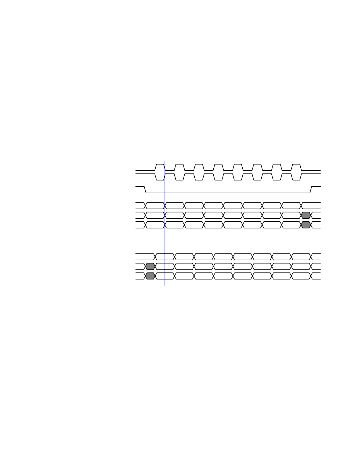
NXP Semiconductors
QN902x
User Manual of QN902x
UM10996
All information provided in this document is subject to legal disclaimers.
© NXP Semiconductors N.V. 2018. All rights reserved.
User Manual
Rev 1.3 — 05 November 2018
77 of 128
The SPI master can connect to two slave devices, and select one slave device to
communicate by setting MSTR_SSx(CR0[14:15]). Only one slave device should be selected
at a time.
10.2.2 Slave Mode Operation
The SPI interface is programmed as a slave device by setting SPI_MODE to 1. If the slave
is selected by a master device via nCS, the data are shifted in through the DIN pin and out
through the DAT pin, clocked by the SCK signal from the master device. The slave device
cannot initiate the data transfer. Data to be transferred to the master device is pre-loaded
into the TX buffer by writing to TXD.
10.2.3 Timing
SPI master support 4 modes, the timing diagram is the same for master and slave as
follows.
CPOL = 0
CPOL = 1
SCK
SS
Cycle #
Data Out
Data In
Cycle #
Data Out
Data In
CPHA=1
CPHA=0
Data captured at the SCK leading edge
Data propagated at the SCK trailing edge
1 2 3 4 5 6 7 8
1Z Z2 3 4 5 6 7 8
1Z Z2 3 4 5 6 7 8
2 3 4 5 6 7 8
1Z Z2 3 4 5 6 7 8
1Z Z2 3 4 5 6 7 8
1
Data propagated at the SCK leading edge
Data captured at the SCK trailing edge
The CPOL defines the logic level when the SPI is idle, while the CPHA defines the active
edge of the SCK to capture the input data.
The SS signal is active low and asserted when the data transfer is initiated by the master
device. It is de-asserted when no more data is in the Tx buffer of master and that last bit
in the shift register is sent out.
10.2.4 Clock generation
The SPI clock is derived by diving the AHB clock as follows:
- USARTx_DIV_BYPASS=1, SPI_CLK=AHB_CLK
- USARTx_DIV_BYPASS=0, SPI_CLK=AHB_CLK/(2*(USARTx_DIVIDER[2:0]+1))
In the master mode, the SCK is generated from the SPI_CLK as shown below:
SCK=SPI_CLK/(2*(BITRATE[5:0]+1))
Page 78

NXP Semiconductors
QN902x
User Manual of QN902x
UM10996
All information provided in this document is subject to legal disclaimers.
© NXP Semiconductors N.V. 2018. All rights reserved.
User Manual
Rev 1.3 — 05 November 2018
78 of 128
The SPI_CLK is also needed by the slave device to operate. The speed should be at least
6 times faster than the SCK frequency of the master device to ensure a reliable
transmission.
Clock
Divider
USART0_DIV_BYPASS
USART0_DIVIDER[2:0]
SPI_CLK0
AHB_CLK SCK0
Clock
Divider
USART1_DIV_BYPASS
USART1_DIVIDER[2:0]
SCK
Generator
SCK
Generator
SCK1
SPI_CLK1
BITRATE[5:0]
BITRATE[5:0]
10.2.5 TX/RX Buffer
Both TX and RX buffer are 32-bit, which can be configured as one 32-bit word buffer, or
4x8-bit FIFO.
10.2.6 Interrupt
When the SPI interrupt is enabled, the following 2 flags will generate an interrupt request:
1. RX buffer not empty interrupt: RX_FIFO_NEPT_IF flag is set to logic 1 if the received
data is moved into RX buffer. The flag is cleared automatically once the RXD is read and
the RX buffer is empty.
2. TX buffer not full interrupt: TX_FIFO_NFUL_IF is set to logic 1 if all data in TX buffer
have been transmitted and the TX buffer can be written again.
10.3 Register Description
10.3.1 Register Map
The SPI0 and SPI1 have the same register map, but different base addresses. The base
address of SPI0 is 0x40007800. The base address of SPI1 is 0x4000A800.
Table 53 SPI0/SPI1 Register Map
Offset
Name
Description
000h
CR0
Control register 0
004h
CR1
Control register 1
008h
RSVD
Reserved
00Ch
RSVD
Reserved
010h
TXD
TX data register
014h
RXD
RX data register
018h
SR
Status register
Page 79

NXP Semiconductors
QN902x
User Manual of QN902x
UM10996
All information provided in this document is subject to legal disclaimers.
© NXP Semiconductors N.V. 2018. All rights reserved.
User Manual
Rev 1.3 — 05 November 2018
79 of 128
10.3.2 Register Description
Table 54 CR0
Bit
Type
Reset
Symbol
Description
31-22 R 0
RSVD
Reserved
21-16
RW 0 BITRATE
Baud rate register, only valid in master mode.
SCK frequency: sck = spi_clk / (2*(BITRATE + 1))
15
RW 0 MSTR_SS1
SS1 select, only valid In master mode
0: de-select
1: select SS1 slave device
14
RW 0 MSTR_SS0
SS0 select, only valid In master mode
0: de-select
1: select SS0 slave device
13-12 R 0
RSVD
11
RW 0 SPI_IE
SPI general interrupt enable
0: disable
1: enable
10 R 0
RSVD
Reserved
9
RW 0 RX_FIFO_NEMT_IE
RX buffer not empty interrupt enable
0: disable
1: enable
8
RW 0 TX_FIFO_NFUL_IE
TX buffer not full interrupt enable
0: disable
1: enable
7
RW 0 DATA_IO_MODE
Data IO mode:
0: 4 wire mode
1: 3 wire mode
6
RW 0 BYTE_ENDIAN
Byte endian, valid only when buffer width is 32:
0: little endian. Send the lower byte first
1: big endian. Send the higher byte first
5
RW 0 BUF_WIDTH
RX/TX buffer width
0: 8 bit
1: 32 bit
4
RW 0 BIT_ORDER
Bit order of byte transfer
1: MSB first
0: LSB first
3 R 0
RSVD
Reserved
2
RW 0 SPI_MODE
SPI mode:
0: master mode
1: slave mode
1
RW 0 CPHA
Data sampling edge of SCK
0 : leading edge (first edge)
1 : trailing edge (second edge)
0
RW 0 CPOL
Logic level of SCK in idle state
0: low
1: high
Table 55 CR1
Bit
Type
Reset
Symbol
Description
Page 80

NXP Semiconductors
QN902x
User Manual of QN902x
UM10996
All information provided in this document is subject to legal disclaimers.
© NXP Semiconductors N.V. 2018. All rights reserved.
User Manual
Rev 1.3 — 05 November 2018
80 of 128
31-18
R 0 RSVD
Reserved
17
W1 0 RX_FF_CLR
Write 1 to clear RX buffer. Not valid to write 0.
16
W1 0 TX_FF_CLR
Write 1 to clear TX buffer. Not valid to write 0.
15-10 R 0
RSVD
Reserved
9
RW 0 S_SDIO_EN
SPI slave data output enable, used only in 3-wire mode, to
control when to switch direction.
1: output
0: input
8
RW 0 M_SDIO_EN
SPI master data output enable, used only in 3-wire mode,
to control when to switch direction.
1: output
0: input
7-0 R 0
RSVD
Reserved
Table 56 TXD
Bit
Type
Reset
Symbol
Description
31:0 W 0
TXD
TX buffer. The width is controlled by BUF_WIDTH.
If BUF_WIDTH=0, the buffer is a 4x8bit FIFO.
If BUF_WIDTH=1, it is a 32-bit buffer.
Table 57 RXD
Bit
Type
Reset
Symbol
Description
31:0 R 0
SPI_RXD
RX buffer. The width is controlled by BUF_WIDTH.
If BUF_WIDTH=0, the buffer is a 4x8bit FIFO.
If BUF_WIDTH=1, it is a 32-bit buffer.
Table 58 SR
Bit
Type
Resst
Symbol
Description
31:25 R 0
RSVD
Reserved
24 R 0
BUSY
SPI bus busy,
0: SS line is high, there is no data transfer
1: SS line is low, there are data transfer
Clear automatically when data is transferred completely
23:17 R 0
RSVD
Reserved
16 R 0
SPI_IF
SPI general interrupt flag.
0: there is not SPI interrupt
1: there are SPI interrupts, cleared automatically when
buffer state changes
15:5 R 0
RSVD
Reserved
4 R 0
RX_FIFO_FULL
RX buffer full flag. Cleared automatically when data is read.
0: RX buffer is not full
1: RX buffer is full
Page 81

NXP Semiconductors
QN902x
User Manual of QN902x
UM10996
All information provided in this document is subject to legal disclaimers.
© NXP Semiconductors N.V. 2018. All rights reserved.
User Manual
Rev 1.3 — 05 November 2018
81 of 128
3 R 0
TX_FIFO_EMPT
TX buffer empty flag. Cleared automatically when data is
put into buffer.
0: There are data in TX buffer
1: There is not data in TX buffer
2 R 0
RSVD
Reserved
1 R 0
RX_FIFO_NEPT_IF
RX buffer not empty flag. Users can read RX data when
buffer is not empty.
0: RX buffer is empty
1: RX buffer is not empty
0 R 0
TX_FIFO_NFUL_IF
TX buffer not full interrupt flag. Can fill in more data when
buffer is not full
0: TX buffer is full
1: TX buffer is not full
Page 82

NXP Semiconductors
QN902x
User Manual of QN902x
UM10996
All information provided in this document is subject to legal disclaimers.
© NXP Semiconductors N.V. 2018. All rights reserved.
User Manual
Rev 1.3 — 05 November 2018
82 of 128
11. TIMERS
QN902X includes four timers. The TIM0 and TIM1 are 32-bit timers, while TIM2 and
TIM3 are 16-bit timers. They can be used for a variety of purposes, including measuring
the pulse width or generating the PWM waveforms.
11.1 Features
32/16-bit auto-reload up counter
16/8-bit capture event counter
10-bit programmable prescaler
Programmable clock sources
Four operation modes
- Free running mode
- Input capture timer mode
- Input capture event mode
- Input capture counter mode
Compare interrupt
Input capture interrupt
Programmable PWM waveform generation
Pulse width, duty and period measurement
Input capture on either positive or negative edge, or both edges
Optional digital noise filtering on capture input
Programmable interrupt period
11.2 Functional Description
The architecture of Timer is shown in the
Figure 10 Timer architecture
.
icp0
icp1
icp2
icp3
acmp
Interrupt
PWM output
Counter
Input
Capture
Waveform Gen.
Compare
Interrupt Gen.
Prescaler
icf
ocf
external clock
clk_timer
Figure 10 Timer architecture
Note: After power on or reset of the QN902x system, the timer is set to its default
values. That means that after QN902x reset, users need to configure register to make
sure that the timer/counter work as required.
Page 83

NXP Semiconductors
QN902x
User Manual of QN902x
UM10996
All information provided in this document is subject to legal disclaimers.
© NXP Semiconductors N.V. 2018. All rights reserved.
User Manual
Rev 1.3 — 05 November 2018
83 of 128
11.2.1 Clock Sources
The timer has two clock sources. One is the pre-scaled clock from clk_timer, which is
generated from the AHB clock. The other one is the external clock input from the GPIO.
The frequency of the scaled clock enable is calculated as follows:
_
1
clk timer
scled
f
f
PSCL
11.2.2 Input Capture Unit
The input capture unit is used to measure duration of the input signal from one edge to
another, in number of clock cycles of the timer clock. The triggering edge can be
configured as a positive edge, negative edge or both edges using the register bits
(ICES[1:0]). When the capture is triggered, the value of the counter is written to the
Capture/Compare Register (CCR). The Input Capture interrupt flag (ICF) is asserted at
the same time as the counter value is copied into the CCR register. If the interrupt is
enabled by register bit ICIE, the input capture flag will generate an interrupt to the
MCU.
To improve the noise immunity on the input signal, a noise canceller is added by using a
simple noise filter scheme, which can be enabled by setting the Input Capture Noise
Canceller Enable (ICNCE).
11.2.3 Compare Unit
TCNT
32/16-bit
comparator
APB BUS
ocfCCR BufferCCR
cnt_en
Figure 11 Compare Unit
The 32/16-bit comparator continuously compares counter with the Compare/Capture
Register buffer (CCR Buffer). If TCNT equals CCR Buffer, the comparator signals a match.
The match will set the Output Compare Flag (OCF) at the next clock cycle of the timer. If
enabled (OCIE=1), the Output Compare Flag generates an output compare interrupt.
The interrupt can be software-cleared by setting corresponding bit.
The CCR and TOP registers are double buffered for supporting configure compare value
and top value on the fly and generating PWM waveform correctly.
11.2.4 PWM Waveform Generation
The PWM waveform can be generated upon the timer overflow or the compare match.
The period and duty cycle can be programmed.
Page 84

NXP Semiconductors
QN902x
User Manual of QN902x
UM10996
All information provided in this document is subject to legal disclaimers.
© NXP Semiconductors N.V. 2018. All rights reserved.
User Manual
Rev 1.3 — 05 November 2018
84 of 128
11.3 Operation Modes
The operation mode and the behavior of the Timer is defined by the Operation Mode
Select bits (OMS[1:0]). Table 59 summarizes the supported modes of the 32/16 bit
timers.
Table 59 Operation Modes
Mode
OMS[1]
OMS[0]
Mode of Operation
0 0 0
Free Running mode
1 0 1
Input Capture Timer mode
2 1 0
Input Capture Event mode
3 1 1
Input Capture Count mode
11.3.1 Free Running mode
In this mode, the counter will count from zero to the value stored in the TOP Buffer and
then restart from zero. Whenever the counter reaches the value of the TOP Buffer, the
Timer Overflow flag (TOV) will be set and an interrupt will be generated if the interrupt
is enabled by the register bit (OVIE).
The comparison of TCNT and CCR buffer is always active in this mode. Once TCNT equals
to CCR buffer, the Output Compare Flag (OCF) is asserted, and a compare match
interrupt is generated if compare interrupt (OCIE) is enabled.
The PWM waveform is generated when PWM output enable bit (pwm_oe) is set. The
duty and period of the PWM waveform can be controlled by TOPR, CCR and
POL(TCR[14]) registers.
11.3.2 Input Capture Timer mode
The capture timer mode is used to capture the trigger events, and record the timestamp in the CCR. It can be used to calculate the pulse width, the period and the duty.
In this mode, the counter will count from zero and will reset to zero at specified edge of
the input capture signal, which is set by ICCLR(TCR[7] . The level change on the Input
Capture Pin (ICP) will trigger the capture event. The triggering operation is defined by
the Input Capture Edge Select bits (ICES[1:0]).
If the a trigger event occurs happens, the Input Capture Flag (ICF) will be set at the clock
cycle. At the same time, the current counter value will be copied to the CCR, and an
interrupt will be generated if the Input Capture Interrupt Enable bit (ICIE) is set.
11.3.3 Input Capture Event mode
This mode is used to count the number of events during a period defined by the TOP
register. When the event happens, the counter ECNT will be incremented. At the end of
the specified period, an Overflow flag (TOV) will be asserted and the value of ECNT will
be copied to the register ICETR. The timer counter TCNT and event counter ECNT will be
reset to zero and begin a new event counting.
Page 85

NXP Semiconductors
QN902x
User Manual of QN902x
UM10996
All information provided in this document is subject to legal disclaimers.
© NXP Semiconductors N.V. 2018. All rights reserved.
User Manual
Rev 1.3 — 05 November 2018
85 of 128
The event source can be selected from the Input Capture Pin (ICP) or the Analog
Comparator. The event is triggered by the edge change of ICP or ACMP. The edge can be
selected by setting the register bits ICES[1:0]. In this mode, no interrupt will be
generated by the trigger event. The timer overflow interrupt will be generated at the
end of the specified time.
11.3.4 Input Capture Count mode
This mode is used to calculate how long it takes for specified event (defined by
ICES[1:0]) to happen times specified by TOP register.
Once the specific event occurs, the event counter ECNT continually increments and
compares its value with TOP register. Once the ECNT equals to the TOP register, the
input capture flag (ICF) will be asserted. The input capture interrupt will be generated if
the ICIE is set.
11.3.5 Interrupt
The QN902x Timer module has three interrupt sources:
• Input capture interrupt
• Output compare interrupt
• Timer overflow interrupt
All three can be enabled by setting TCR[3:1]. The interrupt flag can be read through IFR register.
All three interrupts are valid in 4 operation modes.
11.4 Register Description
11.4.1 Register Map
The Timer 0/1/2/3 have the same registers with different register base addresses as the
following.
Timer 0: 0x40002000
Timer 1: 0x40003000
Timer 2: 0x40004000
Timer 3: 0x40005000
Table 60 Timer Register Map
Offset
Name
Description
000h
TCR
Timer control register
004h
IFR
Timer interrupt flag register
008h
TOPR
Timer TOP register
00Ch
ICER
Timer input capture event register
010h
CCR
Timer input capture/compare register
014h
TCNT
Timer counter current value register
Page 86

NXP Semiconductors
QN902x
User Manual of QN902x
UM10996
All information provided in this document is subject to legal disclaimers.
© NXP Semiconductors N.V. 2018. All rights reserved.
User Manual
Rev 1.3 — 05 November 2018
86 of 128
11.4.2 Register Description
Table 61 TCR
31
30
29
28
27
26
25
24
23
22
21
20
19
18
17
16
15
14
13
12
11
10
9 8 7 6 5 4 3 2 1
0
RSVD
RSVD
CSS[1]
CSS[0]
RSVD
RSVD
PSCL[9]
PSCL[8]
PSCL[7]
PSCL[6]
PSCL[5]
PSCL[4]
PSCL[3]
PSCL[2]
PSCL[1]
PSCL[0]
PWM_OE
POL
ICNCE
ICSS
ICPS[1]
ICPS[0]
ICES[1]
ICES[0]
ICCLR
CHAIN_EN
OMS[1]
OMS[0]
ICIE
OCIE
TOVIE
TEN
0 0 1 0 0 0 1 1 1 1 1 1 1 1 1 1 0 0 0 0 0 0 0 0 0 0 0 0 0 0 0
1
R
R
RW
RW
R
R
RW
RW
RW
RW
RW
RW
RW
RW
RW
RW
RW
RW
RW
RW
RW
RW
RW
RW
RW
RW
RW
RW
RW
RW
RW
RW
Bit
Type
Reset
Symbol
Description
31-30 R 0
RSVD
Reserved
29-28
RW
10b
CSS
clock sources selection
00b = external input clock;
01b = reserved.
10b, 11b = Clk_timer prescaler clock.
27-26 R 0
RSVD
Reserved
25-16
RW
3FFh
PSCL
prescaler factor
CLK_SCALED = CLK_TIMER/ (PSCL + 1)
Note: when pscl equals to zero, it means non scale.
15 R 0
PWM_OE
PWM output enable
0 = disable;
1 = enable.
14
RW 0 POL
PWM output polarity control.
0 = Set high on compare match, set low at the end of PWM
period;
1 = Set low on compare match, set high at the end of PWM
period.
13
RW 0 ICNCE
Input capture noise canceller enable:
0 = disable;
1 = enable.
12
RW 0 ICSS
Input capture source select:
0 = ICP, input capture pin;
1 = ACMP, Analog comparator output.
11-10
RW 0 ICPS
Input Capture Pin Select
00b = icp0;
01b = icp1;
10b = icp2;
11b = icp3.
9-8
RW 0 ICES
Input capture edge select:
00b = positive edge;
01b = negative edge;
10b = positive and negative edge;
11b = reserved.
7
RW 0 ICCLR
Input Capture clear edge selection.
0 = positive edge;
1 = negative edge.
Page 87

NXP Semiconductors
QN902x
User Manual of QN902x
UM10996
All information provided in this document is subject to legal disclaimers.
© NXP Semiconductors N.V. 2018. All rights reserved.
User Manual
Rev 1.3 — 05 November 2018
87 of 128
6
RW 0 CHAIN_EN
Daisy chain enable:
0 = disabled;
1 = enabled, using the first stage timer's output TOVF as the
second stage timer's input this may be more clear.
5-4
RW 0 OMS
Operation mode select:
00b = Free running timer mode;
01b = Input capture timer mode;
10b = Input capture Event mode;
11b = Input capture Counter mode.
3
RW 0 ICIE
Input capture interrupt enable:
0 = interrupt disabled;
1 = interrupt enabled.
2
RW 0 OCIE
compare interrupt enable:
0 = interrupt disabled;
1 = interrupt enabled.
1
RW 0 TOVIE
Timer/Counter overflow interrupt enable:
0 = interrupt disabled;
1 = interrupt enabled.
0
RW 1 TEN
Timer enable:
0 = disable;
1 = enable.
Table 62 IFR
31
30
29
28
27
26
25
24
23
22
21
20
19
18
17
16
15
14
13
12
11
10
9 8 7 6 5 4 3 2 1
0
RSVD
RSVD
RSVD
RSVD
RSVD
RSVD
RSVD
RSVD
RSVD
RSVD
RSVD
RSVD
RSVD
RSVD
RSVD
RSVD
RSVD
RSVD
RSVD
RSVD
RSVD
RSVD
RSVD
RSVD
RSVD
RSVD
RSVD
RSVD
RSVD
ICF
OCF
TOVF
0 0 0 0 0 0 0 0 0 0 0 0 0 0 0 0 0 0 0 0 0 0 0 0 0 0 0 0 0 0 0
0
R R R R R R R R R R R R R R R R R R R R R R R R R R R R R
RW1
RW1
RW1
Bit
Type
Reset
Symbol
Description
31-3 R 0
RSVD
Reserved
2
RW1 0 ICF
Input capture interrupt flag:
0 = no interrupt occurring;
1 = an interrupt pending.
Write 1 to clear the interrupt.
1
RW1 0 OCF
Output compare interrupt flag:
0 = no interrupt occurring;
1 = an interrupt pending.
Write 1 to clear the interrupt.
0
RW1 0 TOVF
Timer overflow interrupt flag:
0 = no interrupt occurring;
1 = an interrupt pending.
Write 1 to clear the interrupt.
Table 63 TOPR
31
30
29
28
27
26
25
24
23
22
21
20
19
18
17
16
15
14
13
12
11
10
9 8 7 6 5 4 3 2 1
0
Page 88

NXP Semiconductors
QN902x
User Manual of QN902x
UM10996
All information provided in this document is subject to legal disclaimers.
© NXP Semiconductors N.V. 2018. All rights reserved.
User Manual
Rev 1.3 — 05 November 2018
88 of 128
TOPR[31] TOPR[30] TOPR[29] TOPR[28] TOPR[27] TOPR[26] TOPR[25] TOPR[24] TOPR[23] TOPR[22] TOPR[21] TOPR[20] TOPR[19] TOPR[18] TOPR[17] TOPR[16] TOPR[15] TOPR[14] TOPR[13] TOPR[12] TOPR[11] TOPR[10]
TOPR[9]
TOPR[8]
TOPR[7]
TOPR[6]
TOPR[5]
TOPR[4]
TOPR[3]
TOPR[2]
TOPR[1]
TOPR[0]
1 1 1 1 1 1 1 1 1 1 1 1 1 1 1 1 1 1 1 1 1 1 1 1 1 1 1 1 1 1 1
1
RW
RW
RW
RW
RW
RW
RW
RW
RW
RW
RW
RW
RW
RW
RW
RW
RW
RW
RW
RW
RW
RW
RW
RW
RW
RW
RW
RW
RW
RW
RW
RW
Bit
Type
Reset
Symbol
Description
31-0
RW
FFFFFFF
Fh
TOPR[31-0]
Timer TOP register for Free-running and capture event
mode:
The bit-width of TOPR is same as Timer count; it can be 16
or 32 bits.
For capture count mode, The 16 LSB(32-bit timer) or 8 LSB
(16-bit timer) is used to set the count event.
Table 64 ICER
31
30
29
28
27
26
25
24
23
22
21
20
19
18
17
16
15
14
13
12
11
10
9 8 7 6 5 4 3 2 1
0
RSVD
RSVD
RSVD
RSVD
RSVD
RSVD
RSVD
RSVD
RSVD
RSVD
RSVD
RSVD
RSVD
RSVD
RSVD
RSVD
ICER[15]
ICER[14]
ICER[13]
ICER[12]
ICER[11]
ICER[10]
ICER[9]
ICER[8]
ICER[7]
ICER[6]
ICER[5]
ICER[4]
ICER[3]
ICER[2]
ICER[1]
ICER[0]
0 0 0 0 0 0 0 0 0 0 0 0 0 0 0 0 0 0 0 0 0 0 0 0 0 0 0 0 0 0 0
0
R R R R R R R R R R R R R R R R R R R R R R R R R R R R R R R
R
Bit
Type
Reset
Symbol
Description
31-16 R 0
RSVD
reserved
15-0 R 0
ICER
Input Capture Event Register.
In input capture event mode, it’s the event number occurred
during specified time duration.
The bit width of ICER can be 16 bit or 24 bit.
Table 65 CCR
31
30
29
28
27
26
25
24
23
22
21
20
19
18
17
16
15
14
13
12
11
10
9 8 7 6 5 4 3 2 1
0
CCR[31]
CCR[30]
CCR[29]
CCR[28]
CCR[27]
CCR[26]
CCR[25]
CCR[24]
CCR[23]
CCR[22]
CCR[21]
CCR[20]
CCR[19]
CCR[18]
CCR[17]
CCR[16]
CCR[15]
CCR[14]
CCR[13]
CCR[12]
CCR[11]
CCR[10]
CCR[9]
CCR[8]
CCR[7]
CCR[6]
CCR[5]
CCR[4]
CCR[3]
CCR[2]
CCR[1]
CCR[0]
1 1 1 1 1 1 1 1 1 1 1 1 1 1 1 1 1 1 1 1 1 1 1 1 1 1 1 1 1 1 1
1
RWH
RWH
RWH
RWH
RWH
RWH
RWH
RWH
RWH
RWH
RWH
RWH
RWH
RWH
RWH
RWH
RWH
RWH
RWH
RWH
RWH
RWH
RWH
RWH
RWH
RWH
RWH
RWH
RWH
RWH
RWH
RWH
Bit
Type
Reset
Symbol
Description
31-0
RWH
FFFFFFFFh
CCR[31-
0]
Timer input Capture/Compare Register 0:
In free-running mode, it’s used as compare register, setting
by software;
Page 89

NXP Semiconductors
QN902x
User Manual of QN902x
UM10996
All information provided in this document is subject to legal disclaimers.
© NXP Semiconductors N.V. 2018. All rights reserved.
User Manual
Rev 1.3 — 05 November 2018
89 of 128
In Capture Timer and Capture Counter mode, it’s used as
capture register to record the timer counter value read by
software.
The bit-width of CCR is same as Timer count; it can be 16 or
32 bits.
Table 66 CNT
31
30
29
28
27
26
25
24
23
22
21
20
19
18
17
16
15
14
13
12
11
10
9 8 7 6 5 4 3 2 1
0
TCNT[31] TCNT[30] TCNT[29] TCNT[28] TCNT[27] TCNT[26] TCNT[25] TCNT[24] TCNT[23] TCNT[22] TCNT[21] TCNT[20] TCNT[19] TCNT[18] TCNT[17] TCNT[16] TCNT[15] TCNT[14] TCNT[13] TCNT[12] TCNT[11] TCNT[10]
TCNT[9]
TCNT[8]
TCNT[7]
TCNT[6]
TCNT[5]
TCNT[4]
TCNT[3]
TCNT[2]
TCNT[1]
TCNT[0]
0 0 0 0 0 0 0 0 0 0 0 0 0 0 0 0 0 0 0 0 0 0 0 0 0 0 0 0 0 0 0
0
R R R R R R R R R R R R R R R R R R R R R R R R R R R R R R R
R
Bit
Type
Reset
Symbol
Description
31-0 R 0 TCNT[31-0]
Timer counter current value:
Read only. The bit-width of TCNT is same as Timer count; it can
be 16 or 32 bits.
Page 90

NXP Semiconductors
QN902x
User Manual of QN902x
UM10996
All information provided in this document is subject to legal disclaimers.
© NXP Semiconductors N.V. 2018. All rights reserved.
User Manual
Rev 1.3 — 05 November 2018
90 of 128
12. UART
The Universal Asynchronous Receiver Transmitter (UART) is a full-duplex, asynchronous
communication interface that communicates with peripheral devices. The QN902x has
two UARTs which can work and be configured independently. The UART shares pins
with the SPI interface.
12.1 Features
Configurable full-duplex or half-duplex data transmission
Hardware flow control option with nRTS and nCTS pins
Programmable baud rate generator, from 1.2kbps, to 921600bps standard
baud rate
Programmable data order with MSB-first or LSB-first shifting
One or Two Stop bits
Odd, even or no-parity bit generation and detection
Receive and transmit data buffer (one depth)
Configurable over-sampling rate (8 or 16)
Parity, buffer overrun and framing error detection
Transmit and receive interrupts
Support for Direct Memory Access (DMA)
Line break generation and detection
Configurable start- and stop- bit levels
8-bit payload mode: 8-bit data without parity
9-bit payload mode: 8-bit data plus parity
12.2 Functional Description
The UART allows asynchronous, serial communication between the MCU and external
devices. Each UART offers a variety of data formatting options. Dedicated baud rate
generator with 22-bit divisor is included, which can generate a wide range of baud
rates. Receive data buffer allows UART to receive up to 8 bits data before data is lost
and an overflow occurs.
Each UART has five registers. The UART_BAUD is used for the Baud Rate Generator. The
UART_CR is used for data formatting, control, and interrupt functions. The UART_Flag is
used for status functions. The UART_TXD and UART_RXD are used to send and receive
data.
The application software can manage the communication by polling the status flag or
using a dedicated UART interrupt. The main elements of the UART and their interactions
are shown in the following block diagram.
Page 91

NXP Semiconductors
QN902x
User Manual of QN902x
UM10996
All information provided in this document is subject to legal disclaimers.
© NXP Semiconductors N.V. 2018. All rights reserved.
User Manual
Rev 1.3 — 05 November 2018
91 of 128
Write buffer
read buffer
Shift register
Shift register
RX FSM
TX FSM
TXD
RXD
APB
interface
Transmitter
Receiver
Baud16
generator
Any UART bidirectional communication requires a minimum of two pins: Receive Data In
(RXD) and Transmit Data Out (TXD):
RXD: Receive Data Input is the serial data input. Oversampling techniques are used for
data recovery by discriminating between valid incoming data and noise.
TXD: Transmit Data Output is the serial data output. When the transmitter is disabled,
the output pin returns to its I/O port configuration. When the transmitter is enabled and
nothing is to be transmitted, the TX pin is at high level.
12.2.1 Baud Rate Generation
The baud rate generator generates Baud16 clock signal by dividing down the input clock
UARTCLK. The baud rate divisor (BRD) is a 22-bit number consisting of a 16-bit integer
and a 6-bit fractional part. The Baud16 signal is then divided by 16 to give the baud rate:
Baud rate = Baud16/16 = (UARTCLK)/(16*BRD)
If we set the reference clock (UARTCLK) = 4MHz, then the generated baud rate error
can be calculated as follows:
GBRD = integer(UARTCLK/(16*BR)*64+0.5)/64
GBR = UARTCLK/(16*GBRD)
Error = (GBR – BR)/BR*100
where:
BR: Baud Rate
GBRD: Generated baud rate divider
Page 92

NXP Semiconductors
QN902x
User Manual of QN902x
UM10996
All information provided in this document is subject to legal disclaimers.
© NXP Semiconductors N.V. 2018. All rights reserved.
User Manual
Rev 1.3 — 05 November 2018
92 of 128
GBR: Generated baud rate
If the required baud rate is 230400 then:
Baud Rate Divisor = (4×10⁶)/ (16×230400) = 1.085 this means BRDI = 1 and BRDF =
0.085.
Therefore, fractional part, m = integer ((0.085×64) + 0.5) = 5
Generated baud rate divider = 1+5/64 = 1.078
Generated baud rate = (4×10⁶)/ (16×1.078) = 231911
Error = (231911-230400)/230400 × 100 = 0.656%
The maximum error using a 6-bit UARTFBRD Register is equal to 1/64×100 = 1.56%. This
occurs when m = 1, and the error cumulates over 64 clock ticks.
Below table lists the errors for typical baud rates.
Table 67 Generated baud rate error when UARTCLK = 8MHz
Desired baud rate(kbps)
Oversampling rate = 16
Oversampling rate = 8
error%
error%
1.2
0.0025
0.0006
2.4
0.0025
-0.0012
4.8
-0.02
0.0025
9.6
0.01
-0.005
14.4
0.01
0.01
19.2
-0.02
0.01
28.8
0.012
0.01
38.4
0.039
-0.02
57.6
-0.087
0.01
76.8
-0.08
0.04
115.2
-0.087
-0.0799
230.4
-0.08
-0.0799
Table 68 Generated baud rate error when uartclk = 4MHz
Desired baud rate(kbps)
Oversampling rate = 16
Oversampling rate = 8
error%
error%
1.2
0.0025
-0.0012
2.4
-0.005
0.0025
4.8
0.01
-0.005
9.6
-0.02
0.01
14.4
0.007
0.01
19.2
0.04
-0.02
28.8
-0.08
0.01
38.4
-0.08
0.04
Page 93

NXP Semiconductors
QN902x
User Manual of QN902x
UM10996
All information provided in this document is subject to legal disclaimers.
© NXP Semiconductors N.V. 2018. All rights reserved.
User Manual
Rev 1.3 — 05 November 2018
93 of 128
57.6
-0.08
-0.0799
76.8
0.16
-0.0799
115.2
-0.08
-0.0799
230.4
0.656
-0.0799
Table 69 Generated baud rate error when uartclk = 2MHz
Desired baud rate(kbps)
Oversampling rate = 16
Oversampling rate = 8
error%
error%
1.2
-0.008
0.0025
2.4
0.00
-0.005
4.8
-0.02
0.01
9.6
0.0395
-0.02
14.4
-0.083
0.01
19.2
-0.078
0.04
28.8
-0.0798
-0.0799
38.4
0.16
-0.0799
57.6
-0.087
-0.0799
76.8
0.156
0.16
115.2
0.64
-0.0799
230.4
---
0.6441
12.2.2 Data Format
The UART has a number of available options for data formatting, which can be set using
CR (control register). The data transfer begins with the start bit. The CR[LEVEL_INV] is
used to define the start and stop conditions. What follows are the data bits. The order in
which the bits are transmitted (MSB or LSB first) is specified by CR[BIT_ORDER]. Next one
is the parity bit, which can be enabled by CR[PEN]. The UART supports the odd and even
parity checks, which can be selected using CR[EPS] The data transmission ends with one
or two stop bits which can be set using CR[STIP2_EN] .
Figure 19.2 shows the timing for a UART transaction without parity bit enabled. Figure
19.3 shows the timing for a UART transaction with parity enabled (PEN = 1).
Page 94

NXP Semiconductors
QN902x
User Manual of QN902x
UM10996
All information provided in this document is subject to legal disclaimers.
© NXP Semiconductors N.V. 2018. All rights reserved.
User Manual
Rev 1.3 — 05 November 2018
94 of 128
12.2.3 Hardware Flow Control
The hardware flow control uses the Clear-To-Send (nCTS) and Request-To-Send (nRTS)
signals to control the flow of the data between the UART and the peripheral devices.
When the auto-flow is enabled, the remote device is not allowed to send data unless
the UART asserts nRTS. If the UART de-asserts nRTS while the remote device is sending
data, the remote device is allowed to send one additional byte after nRTS is deasserted. An overwrite can occur if the remote device violates this rule. Likewise, the
UART is not allowed to transmit any data unless the remote device asserts nCTS. Using
this feature increases system efficiency and eliminates the possibility of a receive buffer
overwrite error due to the long interrupt latency.
The auto-flow mode can be used in two ways: full auto-flow, automating both nCTS and
nRTS; and half auto-flow, automating only nCTS. To enable the full auto-flow,
CR[CTS_EN] and CR[RTS_EN] bits must be set. To enable the auto-nCTS-only mode,
CR[CTS_EN] bit must be set and CR[RTS_EN] bit cleared.
12.2.3.1 nRTS (UART Output)
When in full auto-flow mode, nRTS is asserted when the UART register is ready to
receive data from the remote transmitter. This assertion occurs when the amount of
received data is below the programmable trigger threshold value. When the amount of
received data reaches the programmable trigger threshold, nRTS is de-asserted. It is reasserted when enough bytes are removed from the buffer to lower the data level below
the trigger threshold.
12.2.3.2 nCTS (UART Input)
When in auto-flow mode, nCTS is asserted by the remote receiver when the receiver is
ready to receive data from the UART. The UART checks nCTS before sending the next
byte of data and does not transmit the byte until nCTS is low. If nCTS goes high while
Page 95

NXP Semiconductors
QN902x
User Manual of QN902x
UM10996
All information provided in this document is subject to legal disclaimers.
© NXP Semiconductors N.V. 2018. All rights reserved.
User Manual
Rev 1.3 — 05 November 2018
95 of 128
the transfer of a byte is in progress, the transmitter completes sending this byte.
12.2.4 Interrupt
With UART0/1 interrupts enabled, an interrupt is generated each time a transmission is
completed (TX_IE is set in UART_CR), or a data byte has been received (RX_IE is set in
UART_CR). The UART0/1 interrupt flags except UART_INT are not cleared by hardware
when the CPU vectors to the interrupt service routine. They must be cleared manually
by software, allowing the software to determine the cause of the UART0/1 interrupt
(transmit complete or receive complete).The UART_INT will be auto cleared by software
when all UART0/1 interrupt flags are cleared.
12.2.5 Programming flow
• The write operation consists of the following steps:
1. If TX flow control is enabled, wait for valid cts_uart_n (low level).
2. Configure UART_TXD register
3. Configure UART_BAUD register
4. Configure UART_CR register
5. Read TX_IE bit in UART_CR register. If TX_IE is 1(TX buffer is empty), then go to step
2, else wait until TX buffer becomes empty.
6. If another data is to be transferred, then configure UART_TXD when TX_IE is 1; else
finish.(if baud rate and control information remain unchanged, then there is no need
to re-configure UART_BAUD and UART_CR )
Page 96

NXP Semiconductors
QN902x
User Manual of QN902x
UM10996
All information provided in this document is subject to legal disclaimers.
© NXP Semiconductors N.V. 2018. All rights reserved.
User Manual
Rev 1.3 — 05 November 2018
96 of 128
Start
Configure
UART_TXD
Configure
UART_BAUD
End
Y
N
Cts_en =1 ?
Cts_uart_n=0?
Y
Config ure
UART_CR
Another data is
transferred?
N Y
TX_STRT_INTR=1?
Y
N
N
Page 97

NXP Semiconductors
QN902x
User Manual of QN902x
UM10996
All information provided in this document is subject to legal disclaimers.
© NXP Semiconductors N.V. 2018. All rights reserved.
User Manual
Rev 1.3 — 05 November 2018
97 of 128
• The read operation consists of the following steps:
1. Configure UART_BAUD
2. Configure UART_CR
3. Receive data after detecting valid start-bit
4. After data is received, read UART_RXD and UART_INT
5. If another data is to be received ,then go to step 1;else set RX_EN in UART_CR 0 and
finish
Page 98

NXP Semiconductors
QN902x
User Manual of QN902x
UM10996
All information provided in this document is subject to legal disclaimers.
© NXP Semiconductors N.V. 2018. All rights reserved.
User Manual
Rev 1.3 — 05 November 2018
98 of 128
Start
End
Config ure
UART_CR
Another data is
received?
N
Y
Start bit is
detected ?
N
Y
Config ure
UART_BAUD
8 bit data
received
finished?
N
Y
Read UART_RXD
and UART_INTR
Set rx_en to low in
UART_CR
Page 99

NXP Semiconductors
QN902x
User Manual of QN902x
UM10996
All information provided in this document is subject to legal disclaimers.
© NXP Semiconductors N.V. 2018. All rights reserved.
User Manual
Rev 1.3 — 05 November 2018
99 of 128
12.3 Register Description
12.3.1 Register Map
The UART0 and UART1 have the same register map, but different base addresses.. The
base address of UART0 is 0x40007000. The base address of UART1 is 0x4000A000.
Table 70 UART0/UART1 Register Map
Offset
Name
Reset
Description
000h
UART_TXD
--
Tx data register
004h
UART_RXD
--
Rx data register
008h
UART_BAUD
0x00000403
Baud rate register
00Ch
UART_CR
0x00000880
Control register
010h
UART_FLAG
0x00000000
Status register
12.3.2 Register Description
Table 71 TXD
Bit
Type
Reset
Symbol
Description
31-8 R 0
RSVD
Reserved
7-0 W 0
TXD
Tx buffer data
Table 72 RXD
Bit
Type
Reset
Symbol
Description
31-8 R 0
RSVD
Reserved
7-0 R 0
RXD
Rx buffer data
Table 73 BAUD
Bit
Type
Reset
Symbol
Description
31-24 R 0
RSVD
Reserved
23-8
RW
08h
BAUD_DIV_INT
The integer baud rate divisor
7-6 R 0
RSVD
Reserved
5-0
RW
03h
BAUD_DIV_FRC
The fractional baud rate divisor
Table 74 CR
Bit
Type
Reset
Symbol
Description
31-23 R 0
RSVD
Reserved
Page 100

NXP Semiconductors
QN902x
User Manual of QN902x
UM10996
All information provided in this document is subject to legal disclaimers.
© NXP Semiconductors N.V. 2018. All rights reserved.
User Manual
Rev 1.3 — 05 November 2018
100 of 128
22
RW 0 UART_IE
UART interrupt enable
0: General UART interrupts are disabled
1: General UART interrupts can be enabled
21
RW 0 BE_IE
Break error interrupt enable
0: Break error interrupt is disabled
1: Break error interrupt is enabled
20
RW 0 PE_IE
Parity error interrupt enable
0: Parity error interrupt is disabled
1: Parity error interrupt is enabled
19
RW 0 FE_IE
Framing error interrupt enable
0: Framing error interrupt is disabled
1: Framing error interrupt is enabled
18
RW 0 OE_IE
Overrun error interrupt enable
0: Overrun error interrupt is disabled
1: Overrun error interrupt is enabled
17
RW 0 TX_IE
Transmit status interrupt enable
0: Transmit status interrupt is disable
1: Transmit status interrupt is enabled
16
RW 0 RX_IE
Receive interrupt status enable
0: Receive interrupt status is disable
1: Receive interrupt status is enabled
15-12
RW 0 RSVD
Reserved
11
RW 1 OVS
Oversampling rate.
1 = indicates oversampling rate is 16
0 = indicates oversampling rate is 8
10
RW 0 CTS_EN
CTS hardware flow control enable.
0: CTS hardware flow control is disabled
1: CTS hardware flow control is enabled
9
RW 0 RTS_EN
RTS hardware flow control enable.
0: CTS hardware flow control is disabled
1: CTS hardware flow control is enabled
8
RW 0 BREAK
Send break. Causes a break condition to be
transmitted to the receiving UART.
0: No effect on TXD output
1: Forces TXD output to 0, after completing
transmission of the current character. When TXD
line is idle, one frame low level is transmitted on
line if this bit is set to 1.
For normal use, this bit must be cleared to 0.
7
RW
1
LEVEL_INV
The level of start bit and stop bit
1 = indicates valid start bit is low level and valid
stop bit is high level
0 = indicates valid start bit is high level and valid
stop bit is low level
6
RW 0 STP2_EN
Two stop bits select.
0: 1 stop bit at end of the frame
1: 2 stop bits at the end of frame
5
RW
0
BIT_ORDER
MSB/LSB transmit/receive first
1 = LSB first in the data frame
0 = MSB first in the data frame
4
RW 0 PEN
Parity enable:
0 = parity is disabled and no parity bit added to
the data frame
1 = parity checking and generation is enabled.
 Loading...