


PDTA124E series
PNP resistor-equipped transistors;
R1 = 22 k
Rev. 8 — 25 November 2011 Product data sheet
1. Product profile
1.1 General description
PNP Resistor-Equipped Transistor (RET) family in Surface-Mounted Device (SMD) plastic
packages.
Table 1. Product overview
Type number Package NPN
PDTA124EE SOT416 SC-75 - PDTC124EE ultra small
PDTA124EM SOT883 SC-101 - PDTC124EM leadless ultra small
PDTA124ET SOT23 - TO-236AB PDTC124ET small
PDTA124EU SOT323 SC-70 - PDTC124EU very small
, R2 = 22 k
NXP JEITA JEDEC
complement
Package
configuration
1.2 Features and benefits
100 mA output current capability Reduces component count
Built-in bias resistors Reduces pick and place costs
Simplifies circuit design AEC-Q101 qualified
1.3 Applications
Digital applications in automotive and
industrial segments
Cost-saving alternative for BC847/857
series in digital applications
Control of IC inputs Switching loads
1.4 Quick reference data
Table 2. Quick reference data
Symbol Parameter Conditions Min Typ Max Unit
V
CEO
I
O
R1 bias resistor 1 (input) 15.4 22 28.6 k
R2/R1 bias resistor ratio 0.8 1 1.2
collector-emitter voltage open base - - 50 V
output current - - 100 mA
NXP Semiconductors
006aaa144
12
3
sym003
3
2
1
R1
R2
3
1
2
Transparent
top view
sym003
3
2
1
R1
R2
PDTA124E series
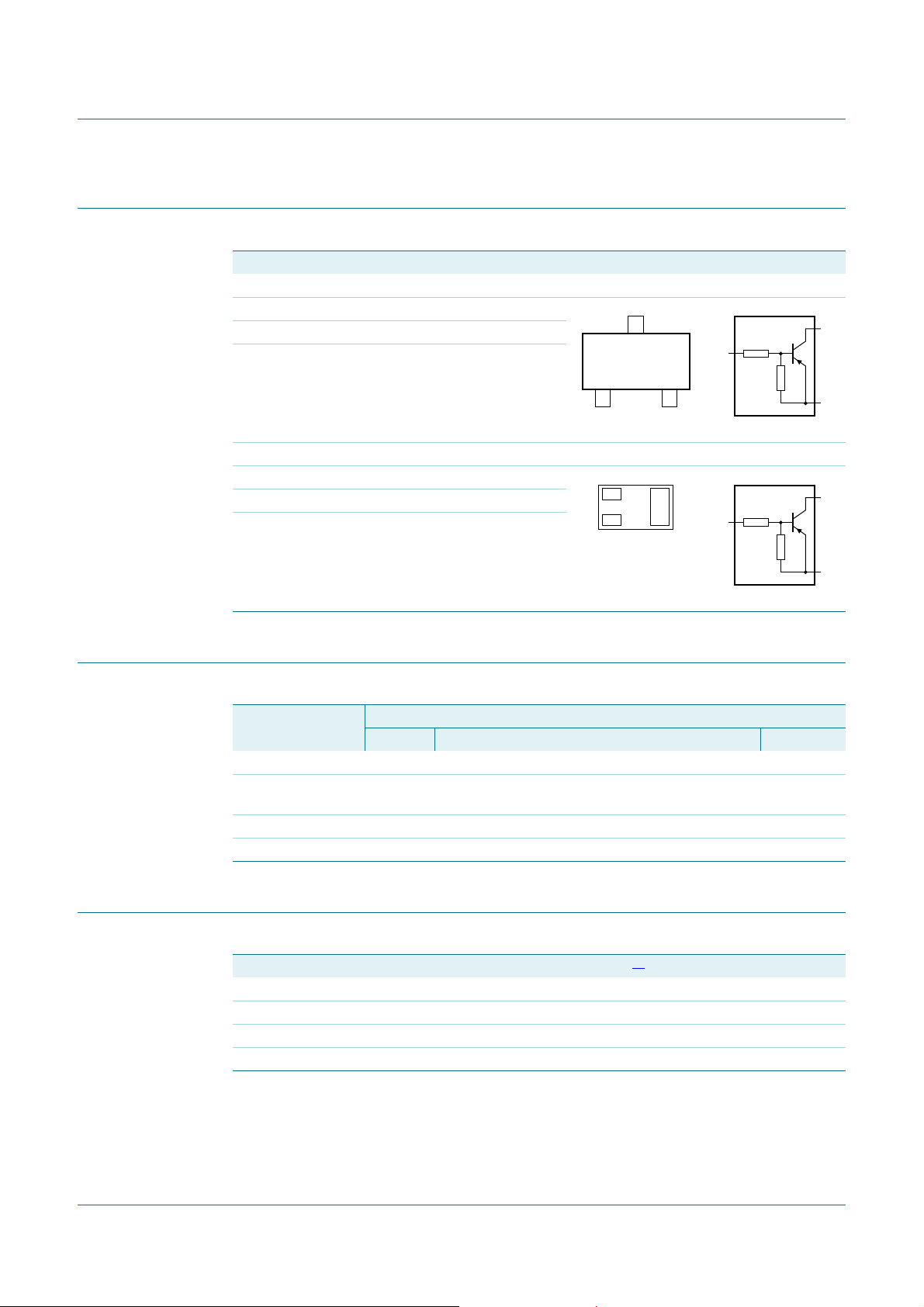
2. Pinning information
Table 3. Pinning
Pin Description Simplified outline Graphic symbol
SOT23; SOT323; SOT416
1 input (base)
2 GND (emitter)
3 output (collector)
SOT883
1 input (base)
2 GND (emitter)
3 output (collector)
PNP resistor-equipped transistors; R1 = 22 k
, R2 = 22 k
3. Ordering information
Table 4. Ordering information
Type number Package
PDTA124EE SC-75 plastic surface-mounted package; 3 leads SOT416
PDTA124EM SC-101 leadless ultra small plastic package; 3 solder lands;
PDTA124ET - plastic surface-mounted package; 3 leads SOT23
PDTA124EU SC-70 plastic surface-mounted package; 3 leads SOT323
4. Marking
Table 5. Marking codes
Type number Marking code
PDTA124EE 05
PDTA124EM DH
PDTA124ET *05
PDTA124EU *05
[1] * = placeholder for manufacturing site code
Name Description Version
SOT883
body 1.0 0.6 0.5 mm
[1]
PDTA124E_SER All information provided in this document is subject to legal disclaimers. © NXP B.V. 2011. All rights reserved.
Product data sheet Rev. 8 — 25 November 2011 2 of 17

NXP Semiconductors
PDTA124E series
5. Limiting values
Table 6. Limiting values
In accordance with the Absolute Maximum Rating System (IEC 60134).
Symbol Parameter Conditions Min Max Unit
V
CBO
V
CEO
V
EBO
V
I
I
O
I
CM
P
tot
T
j
T
amb
T
stg
[1] Device mounted on an FR4 Printed-Circuit Board (PCB), single-sided copper, tin-plated and standard
footprint.
[2] Reflow soldering is the only recommended soldering method.
[3] Device mounted on an FR4 PCB with 70 m copper strip line, standard footprint.
PNP resistor-equipped transistors; R1 = 22 k
, R2 = 22 k
collector-base voltage open emitter - 50 V
collector-emitter voltage open base - 50 V
emitter-base voltage open collector - 10 V
input voltage
positive - +10 V
negative - 40 V
output current - 100 mA
peak collector current single pulse;
1ms
t
p
total power dissipation T
amb
25 C
PDTA124EE (SOT416)
PDTA124EM (SOT883)
PDTA124ET (SOT23)
PDT A124EU (SOT323)
- 100 mA
[1][2]
-150mW
[2][3]
-250mW
[1]
-250mW
[1]
-200mW
junction temperature - 150 C
ambient temperature 65 +150 C
storage temperature 65 +150 C
PDTA124E_SER All information provided in this document is subject to legal disclaimers. © NXP B.V. 2011. All rights reserved.
Product data sheet Rev. 8 — 25 November 2011 3 of 17
NXP Semiconductors
PDTA124E series
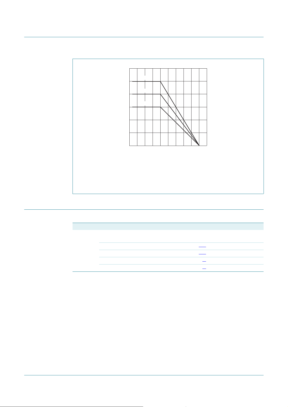
300
P
tot
(mW)
200
100
0
-75 17512525 75-25
(1) SOT23; FR4 PCB, standard footprint
SOT883; FR4 PCB with 70 m copper strip line, standard footprint
(2) SOT323; FR4 PCB, standard footprint
(3) SOT416; FR4 PCB, standard footprint
Fig 1. Power derating curves
PNP resistor-equipped transistors; R1 = 22 k
006aac778
(1)
(2)
(3)
T
(°C)
amb
, R2 = 22 k
6. Thermal characteristics
Table 7. Thermal characteristics
Symbol Parameter Conditions Min Typ Max Unit
R
th(j-a)
[1] Device mounted on an FR4 PCB, single-sided copper, tin-plated and standard footprint.
[2] Reflow soldering is the only recommended soldering method.
[3] Device mounted on an FR4 PCB with 70 m copper strip line, standard footprint.
thermal resistance from junction
to ambient
PDTA124EE (SOT416)
PDTA124EM (SOT883)
PDTA124ET (SOT23)
PDT A124EU (SOT323)
in free air
[1][2]
--830K/W
[2][3]
--500K/W
[1]
--500K/W
[1]
--625K/W
PDTA124E_SER All information provided in this document is subject to legal disclaimers. © NXP B.V. 2011. All rights reserved.
Product data sheet Rev. 8 — 25 November 2011 4 of 17
NXP Semiconductors
006aac782
10
-5
1010
-2
10
-4
10
2
10
-1
tp (s)
10
-3
10
3
1
10
2
10
10
3
Z
th(j-a)
(K/W)
1
duty cycle = 1
0.75
0.5
0.33
0.2
0.1
0.05
0.02
0.01
0
PDTA124E series
PNP resistor-equipped transistors; R1 = 22 k
3
10
duty cycle = 1
Z
Fig 2. Transient thermal impedance from junction to ambient as a function of pulse duration for
0.75
th(j-a)
(K/W)
10
2
10
1
-5
10
0.33
0.1
0.02
0
0.5
0.2
0.05
0.01
-4
10
10
FR4 PCB, standard footprint
PDTA124EE (SOT416); typical values
-3
-2
-1
10
1
1010
2
10
, R2 = 22 k
006aac781
3
10
tp (s)
FR4 PCB, 70m copper strip line
Fig 3. Transient thermal impedance from junction to ambient as a function of pulse duration for
PDTA124EM (SOT883); typical values
PDTA124E_SER All information provided in this document is subject to legal disclaimers. © NXP B.V. 2011. All rights reserved.
Product data sheet Rev. 8 — 25 November 2011 5 of 17
NXP Semiconductors
PDTA124E series
PNP resistor-equipped transistors; R1 = 22 k
3
10
duty cycle = 1
Z
th(j-a)
0.75
(K/W)
2
10
10
1
-5
10
FR4 PCB, standard footprint
Fig 4. Transient thermal impedance from junction to ambient as a function of pulse duration for
PDTA124ET (SOT23); typical values
0.33
0.1
0.02
0
0.5
0.2
0.05
0.01
-4
10
-3
10
-2
-1
10
1
1010
2
10
, R2 = 22 k
006aac779
3
10
tp (s)
3
10
duty cycle = 1
Zth(j-a)
(K/W)
10
0.75
0.5
0.33
2
10
1
-5
10
0.1
0.02
0
0.2
0.05
0.01
-4
10
-3
10
-2
-1
10
1
1010
2
10
FR4 PCB, standard footprint
Fig 5. Transient thermal impedance from junction to ambient as a function of pulse duration for
PDTA124EU (SOT323); typical values
006aac780
tp (s)
3
10
PDTA124E_SER All information provided in this document is subject to legal disclaimers. © NXP B.V. 2011. All rights reserved.
Product data sheet Rev. 8 — 25 November 2011 6 of 17

NXP Semiconductors
PDTA124E series
7. Characteristics
Table 8. Characteristics
T
amb
Symbol Parameter Conditions Min Typ Max Unit
I
CBO
I
CEO
I
EBO
h
FE
V
CEsat
V
I(off)
V
I(on)
R1 bias resistor 1 (input) 15.4 22 28.6 k
R2/R1 bias resistor ratio 0.8 1 1.2
C
c
f
T
PNP resistor-equipped transistors; R1 = 22 k
=25C unless otherwise specified.
collector-base cut-off
current
collector-emitter
cut-off current
emitter-base cut-off
current
DC current gain VCE= 5V; IC= 5mA 60 - collector-emitter
saturation voltage
off-state input voltage VCE= 5V; IC= 100 A- 1.1 0.8 V
on-state input voltage VCE= 0.3 V; IC= 5mA 2.5 1.7 - V
collector capacitance VCB= 10 V; IE=ie=0A;
transition frequency VCE= 5V; IC= 10 mA;
VCB= 50 V; IE=0A - - 100 nA
VCE= 30 V; IB=0A - - 100 nA
= 30 V; IB=0A;
V
CE
--5 A
Tj= 150 C
VEB= 5V; IC=0A - - 180 A
IC= 10 mA; IB= 0.5 mA - - 150 mV
--3pF
f=1MHz
[1]
-180-MHz
f = 100 MHz
, R2 = 22 k
[1] Characteristics of built-in transistor
3
10
h
FE
2
10
10
1
-1
-10
006aac800
(1)
(2)
(3)
2
-10-1
IC (mA)
-10
VCE= 5V
(1) T
(2) T
(3) T
amb
amb
amb
= 100 C
=25C
= 40 C
Fig 6. DC current gain as a function of collector
current; typical values
006aac801
(1)
2
-10-1
IC (mA)
-10
V
CEsat
-1
(V)
-1
-10
-2
-10
(1) T
(2) T
(3) T
-10
I
-1
C/IB
amb
amb
amb
(2)
(3)
=20
= 100 C
=25C
= 40 C
Fig 7. Collector-emitter saturation voltage as a
function of collector current; typical values
PDTA124E_SER All information provided in this document is subject to legal disclaimers. © NXP B.V. 2011. All rights reserved.
Product data sheet Rev. 8 — 25 November 2011 7 of 17

NXP Semiconductors
PDTA124E series
-10
V
I(on)
(V)
-1
-1
-10
-1
-10
006aac802
(1)
(2)
(3)
-10-1
IC (mA)
-10
VCE= 0.3 V
amb
amb
amb
= 40 C
=25C
= 100 C
(1) T
(2) T
(3) T
Fig 8. On-state input voltage as a function of
collector current; typical values
PNP resistor-equipped transistors; R1 = 22 k
-10
V
I(off)
(V)
(1)
-1
-1
2
-10
-10
(1) T
(2) T
(3) T
-1
V
CE
amb
amb
amb
= 5V
= 40 C
=25C
= 100 C
Fig 9. Off-state input voltage as a function of
collector current; typical values
(2)
(3)
IC (mA)
, R2 = 22 k
006aac803
-10-1
006aac804
VCB (V)
C
(pF)
6
c
4
2
0
0 -50-40-20 -30-10
f=1MHz; T
=25CV
amb
Fig 10. Collector capacitance as a function of
collector-base voltage; typical values
10
f
T
(MHz)
10
10
3
2
-10
-1
= 5V; T
CE
amb
=25C
006aac763
2
-10-1
IC (mA)
-10
Fig 11. Transition frequency as a function of collector
current; typical values of built-in transistor
PDTA124E_SER All information provided in this document is subject to legal disclaimers. © NXP B.V. 2011. All rights reserved.
Product data sheet Rev. 8 — 25 November 2011 8 of 17

NXP Semiconductors
04-11-04Dimensions in mm
0.95
0.60
1.8
1.4
1.75
1.45
0.9
0.7
0.25
0.10
1
0.30
0.15
12
3
0.45
0.15
03-04-03Dimensions in mm
0.62
0.55
0.55
0.47
0.50
0.46
0.65
0.20
0.12
3
21
0.30
0.22
0.30
0.22
1.02
0.95
0.35
04-11-04Dimensions in mm
0.45
0.15
1.9
1.1
0.9
3.0
2.8
2.5
2.1
1.4
1.2
0.48
0.38
0.15
0.09
12
3
04-11-04Dimensions in mm
0.45
0.15
1.1
0.8
2.2
1.8
2.2
2.0
1.35
1.15
1.3
0.4
0.3
0.25
0.10
12
3
PDTA124E series
8. Test information
8.1 Quality information
This product has been qualified in accordance with the Automotive Electronics Council
(AEC) standard Q101 - Stress test qualification for discrete semiconductors, and is
suitable for use in automotive applications.
9. Package outline
PNP resistor-equipped transistors; R1 = 22 k
, R2 = 22 k
Fig 12. Package outline PDTA124EE (SOT416/SC-75) Fig 13. Package outline PDTA124EM (SOT883/SC-101)
Fig 14. Package outline PDTA124ET (SOT23) Fig 15. Package outline PDTA124EU (SOT323/SC-70)
PDTA124E_SER All information provided in this document is subject to legal disclaimers. © NXP B.V. 2011. All rights reserved.
Product data sheet Rev. 8 — 25 November 2011 9 of 17

NXP Semiconductors
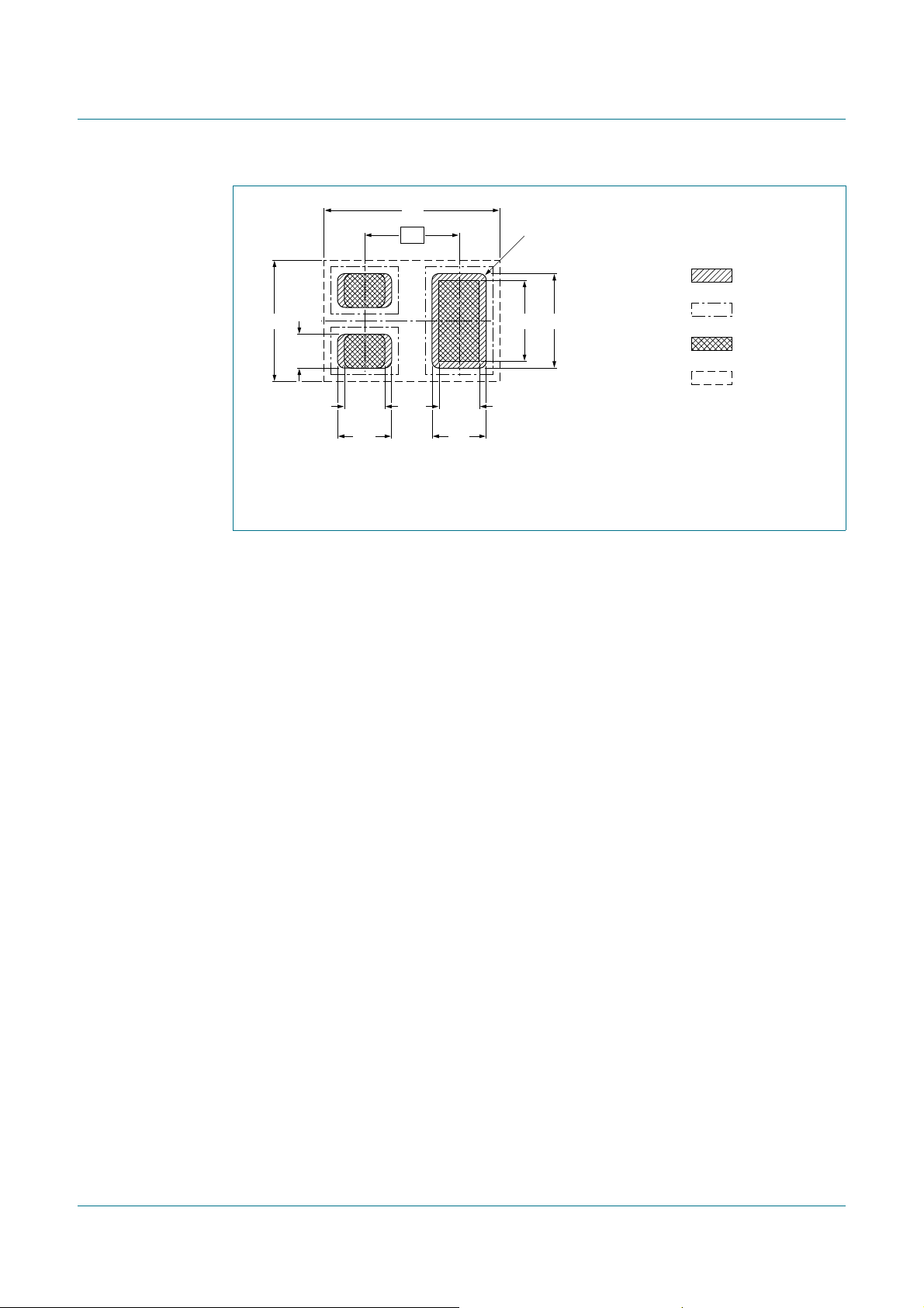
solder lands
solder resist
occupied area
solder paste
sot416_fr
0.85
1.7
2.2
2
0.5
(3×)
0.6
(3×)
1
1.3
Dimensions in mm
PDTA124E series
PNP resistor-equipped transistors; R1 = 22 k
, R2 = 22 k
10. Packing information
Table 9. Packing methods
The indicated -xxx are the last three digits of the 12NC ordering code.
Type number Package Description Packing quantity
PDTA124EE SOT416 4 mm pitch, 8 mm tape and reel -1 15 - -135
PDTA124EM SOT883 2 mm pitch, 8 mm tape and reel - - -315
PDTA124ET SOT23 4 mm pitch, 8 mm tape and reel -215 - -235
PDTA124EU SOT323 4 mm pitch, 8 mm tape and reel -115 - -135
[1] For further information and the availability of packing methods, see Section 14.
[1]
3000 5000 10000
11. Soldering
Reflow soldering is the only recommended soldering method.
Fig 16. Reflow soldering footprint PDTA124EE (SOT416/SC-75)
PDTA124E_SER All information provided in this document is subject to legal disclaimers. © NXP B.V. 2011. All rights reserved.
Product data sheet Rev. 8 — 25 November 2011 10 of 17
NXP Semiconductors
solder lands
solder resist
occupied area
solder paste
sot883_fr
1.3
0.3
0.6
0.7
0.4
0.9
0.3
(2×)
0.4
(2×)
0.25
(2×)
R0.05 (12×)
0.7
Dimensions in mm
PDTA124E series
PNP resistor-equipped transistors; R1 = 22 k
Reflow soldering is the only recommended soldering method.
Fig 17. Reflow soldering footprint PDTA124EM (SOT883/SC-101)
, R2 = 22 k
PDTA124E_SER All information provided in this document is subject to legal disclaimers. © NXP B.V. 2011. All rights reserved.
Product data sheet Rev. 8 — 25 November 2011 11 of 17

NXP Semiconductors
solder lands
solder resist
occupied area
solder paste
sot023_fr
0.5
(3×)
0.6
(3×)
0.6
(3×)
0.7
(3×)
3
1
3.3
2.9
1.7
1.9
2
Dimensions in mm
solder lands
solder resist
occupied area
preferred transport direction during soldering
sot023_fw
2.8
4.5
1.4
4.6
1.4
(2×)
1.2
(2×)
2.2
2.6
Dimensions in mm
PDTA124E series
PNP resistor-equipped transistors; R1 = 22 k
, R2 = 22 k
Fig 18. Reflow soldering footprint PDTA124ET (SOT23)
PDTA124E_SER All information provided in this document is subject to legal disclaimers. © NXP B.V. 2011. All rights reserved.
Product data sheet Rev. 8 — 25 November 2011 12 of 17
Fig 19. Wave soldering footprint PDTA124ET (SOT23)

NXP Semiconductors
solder lands
solder resist
occupied area
solder paste
sot323_fr
2.65
2.35
0.6
(3×)
0.5
(3×)
0.55
(3×)
1.325
1.85
1.3
3
2
1
Dimensions in mm
sot323_fw
3.65 2.1
1.425
(3×)
4.6
09
(2×)
2.575
1.8
solder lands
solder resist
occupied area
preferred transport
direction during soldering
Dimensions in mm
PDTA124E series
PNP resistor-equipped transistors; R1 = 22 k
Fig 20. Reflow soldering footprint PDTA124EU (SOT323/SC-70)
, R2 = 22 k
Fig 21. Wave soldering footprint PDTA124EU (SOT323/SC-70)
PDTA124E_SER All information provided in this document is subject to legal disclaimers. © NXP B.V. 2011. All rights reserved.
Product data sheet Rev. 8 — 25 November 2011 13 of 17

NXP Semiconductors
PDTA124E series
PNP resistor-equipped transistors; R1 = 22 k
, R2 = 22 k
12. Revision history
Table 10. Revision history
Document ID Release date Data sheet status Change notice Supersedes
PDTA124E_SER v.8 20111125 Product data sheet - PDTA124E_SERIES v.7
Modifications:
PDTA124E_SERIES v.7 20040805 Product data sheet - PDTA124E_SERIES v.6
PDTA124E_SERIES v.6 20030414 Product specification - -
• The format of this document has been redesigned to comply with the new identity
guidelines of NXP Semiconductors.
• Legal texts have been adapted to the new company name where appropriate.
• Ty pe numbers PDTA12 4EEF, PDTA124EK and PDTA124ES removed.
Section 1 “Product profile”: updated
•
•
Section 3 “Ordering information”: added
Section 4 “Marking”: updated
•
Figure 1 to 11: added
•
•
Section 6 “Thermal characteristics”: updated
Table 8 “Characteristics”: V
•
V
off-state input voltage, I
I(off)
•
Section 8 “Test information ”: added
Section 9 “Package outline”: superseded by minimized package outline drawings
•
Section 10 “Packing information”: added
•
•
Section 11 “Soldering”: added
Section 13 “Legal information”: updated
•
redefined to V
i(on)
updated, fT added
CEO
on-state input voltage, V
I(on)
redefined to
i(off)
PDTA124E_SER All information provided in this document is subject to legal disclaimers. © NXP B.V. 2011. All rights reserved.
Product data sheet Rev. 8 — 25 November 2011 14 of 17

NXP Semiconductors
PDTA124E series
PNP resistor-equipped transistors; R1 = 22 k
, R2 = 22 k
13. Legal information
13.1 Data sheet status
Document status
Objective [short] data sheet Development This document contains data from the objective specification for product development.
Preliminary [short] data sheet Qualification This document contains data from the preliminary specification.
Product [short] data sheet Production This document contains the product specification.
[1] Please consult the most recently issued document before initiating or completing a design.
[2] The term ‘short data sheet’ is explained in section “Definitions”.
[3] The product status of device(s) described in this docu ment may have change d since this d ocument was p ublished and may dif fe r in case of multiple devices. The latest product status
information is available on the Internet at URL
13.2 Definitions
Draft — The document is a draft version only. The content is still under
internal review and subject to formal approval, which may result in
modifications or additions. NXP Semiconductors does not give any
representations or warranties as to the accuracy or completeness of
information included herein and shall have no liability for the consequences of
use of such information.
Short data sheet — A short data sheet is an extract from a full data sheet
with the same product type number(s) and title. A short data sheet is intended
for quick reference only and should not be relied upon to co nt ain det ailed and
full information. For detailed and full information see the relevant full data
sheet, which is available on request via the local NXP Semiconductors sales
office. In case of any inconsistency or conflict with the short data sheet, the
full data sheet shall prevail.
Product specification — The information and data provided in a Product
data sheet shall define the specification of the product as agreed between
NXP Semiconductors and its customer, unless NXP Semiconductors and
customer have explicitly agreed otherwise in writing. In no event however,
shall an agreement be valid in which the NXP Semiconductors product is
deemed to offer functions and qualities beyond those described in the
Product data sheet.
13.3 Disclaimers
Limited warranty and liability — Information in this document is believed to
be accurate and reliable. However, NXP Semiconductors does not give any
representations or warranties, expressed or implied, as to the accuracy or
completeness of such information and shall have no liability for the
consequences of use of such information.
In no event shall NXP Semiconductors be liable for any indirect, incidental,
punitive, special or consequential damages (including - without limitation - lost
profits, lost savings, business interruption, costs related to the removal or
replacement of any products or rework charges) whether or not such
damages are based on tort (including negligence), warranty, breach of
contract or any other legal theory.
Notwithstanding any damages that customer might incur for any reason
whatsoever, NXP Semi conductors’ aggregat e and cumulative liabil ity towards
customer for the products described herein shall be limited in accordance
with the Terms and conditions of commercial sale of NXP Semiconductors.
Right to make changes — NXP Semiconductors reserves the right to make
changes to information published in this document, including without
limitation specifications and product descriptions, at any time and without
notice. This document supersedes and replaces all information supplied prior
to the publication hereof.
Suitability for use — NXP Semiconductors products are not designed,
authorized or warranted to be suitable for use in life support, life-critical or
safety-critical systems or equipment, nor in applications where failure or
[1][2]
Product status
http://www.nxp.com.
[3]
Definition
malfunction of an NXP Semiconductors product can reasonably be expected
to result in personal injury, death or severe property or environment al
damage. NXP Semiconductors accepts no liability for inclusion and/or use of
NXP Semiconductors products in such equipment or applications and
therefore such inclusion and/or use is at the customer’s own risk.
Applications — Applications that are described herein for any of these
products are for illustrative purposes only. NXP Semiconductors makes no
representation or warranty that such applications will be suitable for the
specified use without further testing or modification.
Customers are responsible for the design and operation of their applications
and products using NXP Semiconductors products, and NXP Semiconductors
accepts no liability for any assistance with applications or cust omer product
design. It is customer’s sole responsibility to determine whether the NXP
Semiconductors product is suitable and fit for the customer’s applications and
products planned, as well as for the planned application and use of
customer’s third party customer(s). Customers should provide appropriate
design and operating safeguards to minimize the risks associated with their
applications and products.
NXP Semiconductors does not accept any liability related to any default ,
damage, costs or problem which is based on any weakness or default in the
customer’s applications or products, or the application or use by customer’s
third party customer(s). Customer is responsible for doing all necessary
testing for the customer’s applications and products using NXP
Semiconductors products in order to avoid a default of the applications and
the products or of the application or use by customer’s third part y
customer(s). NXP does not accept any liability in this respect.
Limiting values — Stress above one or more limiting values (as defined in
the Absolute Maximum Ratings System of IEC 60134) will cause permanent
damage to the device. Limiting values are stress ratings only and (proper)
operation of the device at these or any other conditions above those given in
the Recommended operating conditions section (if present) or the
Characteristics sections of this document is not warranted. Constant or
repeated exposure to limiting values will permanently and irreversibly affect
the quality and reliability of the device.
Terms and conditions of commercial sale — NXP Semiconductors
products are sold subject to the general terms and conditions of commercial
sale, as published at
agreed in a valid written individual agreement. In case an individual
agreement is concluded only the terms and conditions of the respective
agreement shall apply. NXP Semiconductors hereby expressly objects to
applying the customer’s general terms and conditions with regard to the
purchase of NXP Semiconductors products by customer.
No offer to sell or license — Nothing in this document may be interpreted or
construed as an offer to sell product s that is open for accept ance or the gr ant,
conveyance or implication of any license under any copyrights, patents or
other industrial or intellectual property rights.
Export control — This document as well as the item(s) described herein
may be subject to export control regulations. Export might require a prior
authorization from competent authorities.
http://www.nxp.com/profile/terms
, unless otherwise
PDTA124E_SER All information provided in this document is subject to legal disclaimers. © NXP B.V. 2011. All rights reserved.
Product data sheet Rev. 8 — 25 November 2011 15 of 17

NXP Semiconductors
PDTA124E series
PNP resistor-equipped transistors; R1 = 22 k
Quick reference data — The Quick reference data is an extract of the
product data given in the Limiting values and Characteristics sections of this
document, and as such is not complete, exhaustive or legally binding.
13.4 Trademarks
Notice: All referenced brands, product names, service names and trademarks
are the property of their respective owners.
14. Contact information
For more information, please visit: http://www.nxp.com
For sales office addresses, please send an email to: salesaddresses@nxp.com
, R2 = 22 k
PDTA124E_SER All information provided in this document is subject to legal disclaimers. © NXP B.V. 2011. All rights reserved.
Product data sheet Rev. 8 — 25 November 2011 16 of 17

NXP Semiconductors
PDTA124E series
PNP resistor-equipped transistors; R1 = 22 k
15. Contents
1 Product profile . . . . . . . . . . . . . . . . . . . . . . . . . . 1
1.1 General description . . . . . . . . . . . . . . . . . . . . . 1
1.2 Features and benefits. . . . . . . . . . . . . . . . . . . . 1
1.3 Applications . . . . . . . . . . . . . . . . . . . . . . . . . . . 1
1.4 Quick reference data . . . . . . . . . . . . . . . . . . . . 1
2 Pinning information. . . . . . . . . . . . . . . . . . . . . . 2
3 Ordering information. . . . . . . . . . . . . . . . . . . . . 2
4 Marking. . . . . . . . . . . . . . . . . . . . . . . . . . . . . . . . 2
5 Limiting values. . . . . . . . . . . . . . . . . . . . . . . . . . 3
6 Thermal characteristics . . . . . . . . . . . . . . . . . . 4
7 Characteristics. . . . . . . . . . . . . . . . . . . . . . . . . . 7
8 Test information. . . . . . . . . . . . . . . . . . . . . . . . . 9
8.1 Quality information . . . . . . . . . . . . . . . . . . . . . . 9
9 Package outline . . . . . . . . . . . . . . . . . . . . . . . . . 9
10 Packing information . . . . . . . . . . . . . . . . . . . . 10
11 Soldering . . . . . . . . . . . . . . . . . . . . . . . . . . . . . 10
12 Revision history. . . . . . . . . . . . . . . . . . . . . . . . 14
13 Legal information. . . . . . . . . . . . . . . . . . . . . . . 15
13.1 Data sheet status . . . . . . . . . . . . . . . . . . . . . . 15
13.2 Definitions. . . . . . . . . . . . . . . . . . . . . . . . . . . . 15
13.3 Disclaimers . . . . . . . . . . . . . . . . . . . . . . . . . . . 15
13.4 Trademarks. . . . . . . . . . . . . . . . . . . . . . . . . . . 16
14 Contact information. . . . . . . . . . . . . . . . . . . . . 16
15 Contents . . . . . . . . . . . . . . . . . . . . . . . . . . . . . . 17
, R2 = 22 k
Please be aware that important notices concerning this document and the product(s)
described herein, have been included in section ‘Legal information’.
© NXP B.V. 2011. All rights reserved.
For more information, please visit: http://www.nxp.com
For sales office addresses, please send an email to: salesaddresses@nxp.com
Date of release: 25 November 2011
Document identifier: PDTA124E_SER

 Loading...