

Page 1

MCSPTR2A5775E 3-phase PMSM Motor
NXP Semiconductors
Document Number: AN13038
Application Note
Rev. 0
,
10/2020
Contents
1. Introduction ........................................................................ 1
2. System concept ................................................................... 2
3. PMSM field-oriented control.............................................. 3
3.1. Fundamental principle of PMSM FOC ................... 3
3.2. PMSM model in quadrature phase synchronous
reference frame ...................................................................... 5
3.3. Output voltage actuation and phase current
measurement ......................................................................... 7
3.4. Rotor position/speed estimation .............................. 9
3.5. Field weakening .................................................... 10
4. Software implementation on the MPC5777E ................... 13
4.1. eTPU ..................................................................... 13
4.2. MPC5777E – Key modules for PMSM FOC control
17
4.3. MPC5775E Device initialization ........................... 19
4.4. Software architecture ............................................. 34
5. FreeMASTER and MCAT user interface ......................... 47
5.1. MCAT Settings and Tuning .................................. 48
5.2. MCAT application Control ................................... 51
6. Conclusion ........................................................................ 52
7. References ........................................................................ 52
Control Kit with MPC5775E
Featuring Motor Control Application Tuning (MCAT) Tool
by: NXP Semiconductors
1. Introduction
This application note describes the design of a 3-phase
Permanent Magnet Synchronous Motor (PMSM) vector
control drive with 3-shunt current sensing and resolver
position sensing. The design is targeted for automotive
motor control (MC) applications.
This design serves as an example of motor control design
using NXP family of automotive motor control MCUs
based on a 32-bit Power Architecture technology
optimized for a full range of automotive applications.
Following are the supported features:
• 3-phase PMSM speed Field Oriented Control.
• Current sensing with three shunt resistors.
• Application control user interface using
FreeMASTER debugging tool.
• Motor Control Application Tuning (MCAT) tool.
• Rotor position and speed measurement using
resolver transducer
Page 2

System concept
MCSPTR2A5775E 3-phase PMSM Motor Control Kit with MPC5775E, Rev. 0, 10/2020
2 NXP Semiconductors
2. System concept
The system is designed to drive a 3-phase PM synchronous motor. The application meets the following
performance specifications:
• Targeted at the MPC5775E-EVB Evaluation Board (refer to dedicated user manual for
MPC5775E-EVB available at www.nxp.com). See References for more information
• S32 Design Studio (see References)
• MC33937 MOSFETs pre-driver with extensive set of functions and condition monitoring (see
References)
• Control technique incorporating:
o Field Oriented Control of 3-phase PM synchronous motor with resolver position sensor
o Closed-loop speed control with action period 1 ms
o Closed-loop current control with action period 100 µs
o Bi-directional rotation
o Flux and torque independent control
o Field weakening control extending speed range of the PMSM beyond the base speed
o Position and speed are computed by Enhanced Time Processing Unit eTPU
o Sensing of three-phase motor currents
o FOC state variables sampled with 100 μs period
• Automotive Math and Motor Control Library (AMMCLIB) - FOC algorithm built on blocks of
precompiled SW library (see section References)
• Use of eTPU Motor control function set to offload CPU
• FreeMASTER
o FreeMASTER software control interface (motor start/stop, speed setup)
o FreeMASTER software monitor
o FreeMASTER embedded Motor Control Application Tuning (MCAT) tool (motor
parameters, current loop, speed loop) (see section References)
o FreeMASTER software MCAT graphical control page (required speed, actual motor
speed, start/stop status, DC-Bus voltage level, motor current, system status)
o FreeMASTER software speed scope (observes actual and desired speeds, DC-Bus
voltage and motor current)
o FreeMASTER software high-speed recorder (reconstructed motor currents, vector control
algorithm quantities)
• DC-Bus over-voltage and under-voltage, over-current, overload and start-up fail protection
Page 3
PMSM field-oriented control
MCSPTR2A5775E 3-phase PMSM Motor Control Kit with MPC5775E, Rev. 0, 10/2020
NXP Semiconductors 3
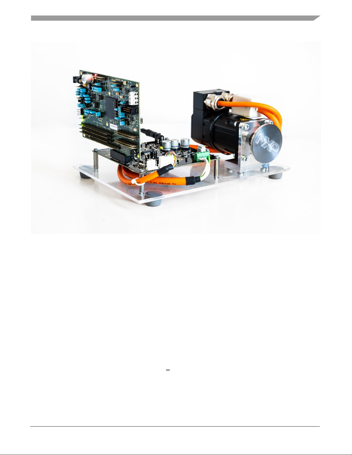
Figure 1 MCSPTR2A5775E 3-phase PMSM Development Kit with MPC5775E
3. PMSM field-oriented control
3.1.
Fundamental principle of PMSM FOC
High-performance motor control is characterized by smooth rotation over the entire speed range of the
motor, full torque control at zero speed, and fast acceleration/deceleration. To achieve such control,
Field Oriented Control is used for PM synchronous motors.
The FOC concept is based on an efficient torque control requirement, which is essential for achieving a
high control dynamic. Analogous to standard DC machines, AC machines develop maximal torque
when the armature current vector is perpendicular to the flux linkage vector. Thus, if only the
fundamental harmonic of stator magnetomotive force is considered, the torque Te developed by an AC
machine, in vector notation, is given by the following equation:
Equation 1
where pp is the number of motor pole-pairs, is is stator current vector and ψs represents vector of the
stator flux. Constant 3/2 indicates a non-power invariant transformation form.
Page 4

PMSM field-oriented control
MCSPTR2A5775E 3-phase PMSM Motor Control Kit with MPC5775E, Rev. 0, 10/2020
4 NXP Semiconductors
In instances of DC machines, the requirement to have the rotor flux vector perpendicular to the stator
current vector is satisfied by the mechanical commutator. Because there is no such mechanical
commutator in AC Permanent Magnet Synchronous Machines (PMSM), the functionality of the
commutator has to be substituted electrically by enhanced current control. This reveal that stator current
vector should be oriented in such a way that component necessary for magnetizing of the machine (flux
component) shall be isolated from the torque producing component.
This can be accomplished by decomposing the current vector into two components projected in the
reference frame, often called the dq frame that rotates synchronously with the rotor. It has become a
standard to position the dq reference frame such that the d-axis is aligned with the position of the rotor
flux vector, so that the current in the d-axis will alter the amplitude of the rotor flux linkage vector. The
reference frame position must be updated so that the d-axis should be always aligned with the rotor flux
axis.
Because the rotor flux axis is locked to the rotor position, when using PMSM machines, a mechanical
position transducer or position observer can be utilized to measure the rotor position and the position of
the rotor flux axis. When the reference frame phase is set such that the d-axis is aligned with the rotor
flux axis, the current in the q-axis represents solely the torque producing current component.
What further resulted from setting the reference frame speed to be synchronous with the rotor flux axis
speed is that both d and q axis current components are DC values. This implies utilization of simple
current controllers to control the demanded torque and magnetizing flux of the machine, thus
simplifying the control structure design.
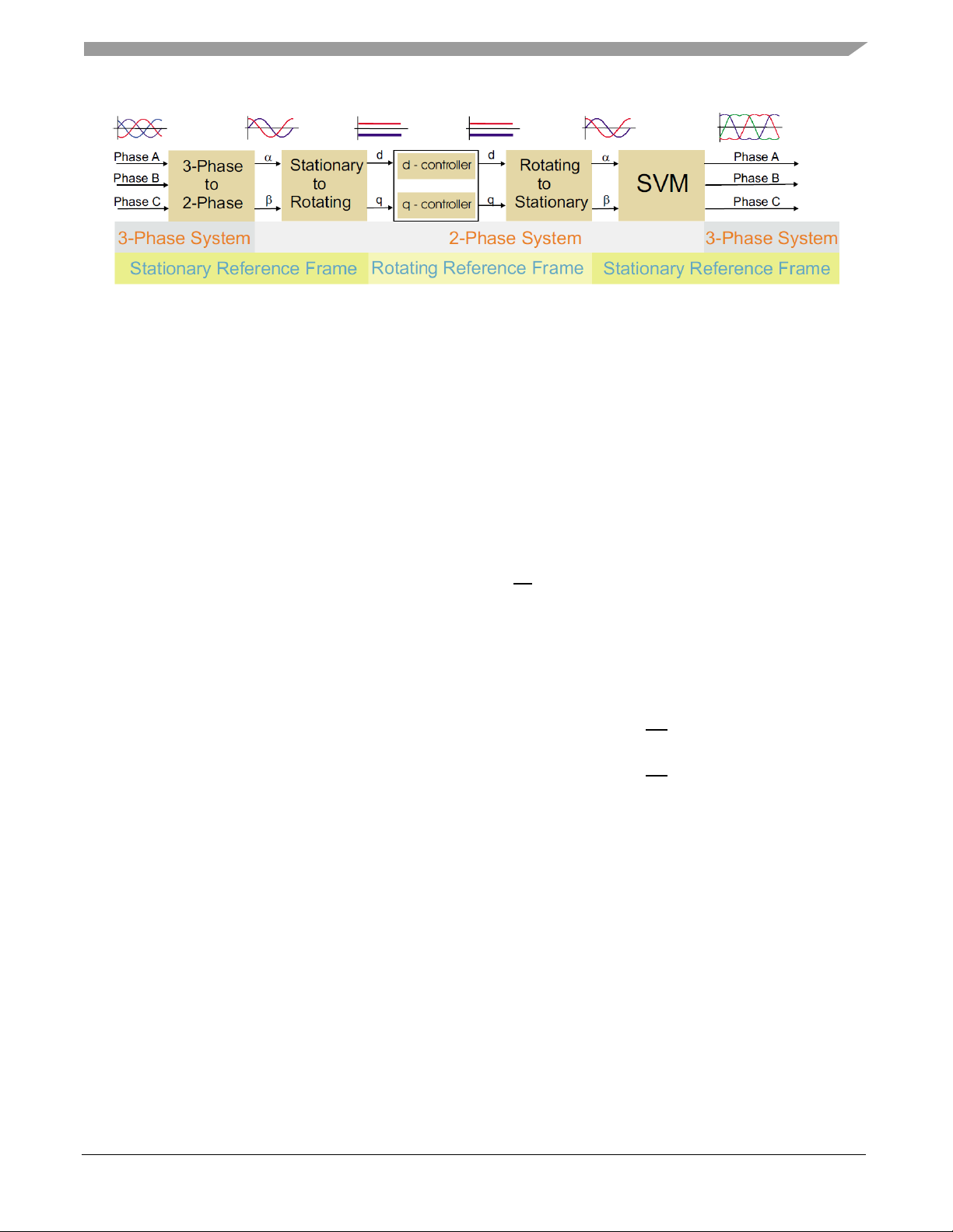
Figure 2 shows the basic structure of the vector control algorithm for the PM synchronous motor. To
perform vector control, it is necessary to take following four steps:
1. Measure the motor quantities (DC link voltage and currents, rotor position/speed).
2. Transform measured currents into the two-phase orthogonal system (α, β) using a Clarke
transformation. After that transform the currents in α, β coordinates into the d, q reference frame
using a Park transformation.
3. The stator current torque (i
sq
) and flux (isd) producing components are separately controlled in d,
q rotating frame.
4. The output of the control is stator voltage space vector and it is transformed by an inverse Park
transformation back from the d, q reference frame into the two-phase orthogonal system fixed
with the stator. The output three-phase voltage is generated using a space vector modulation.
Clarke/Park transformations discussed above are part of the Automotive Math and Motor Control
Library set (see section References).
To be able to decompose currents into torque and flux producing components (isd, isq), position of the
motor-magnetizing flux has to be known. This requires knowledge of the accurate rotor position as
being strictly fixed with magnetic flux. This application note deals with the sensor based FOC control
where the position and velocity are obtained by position/velocity estimator executed by eTPU. Position
and speed are processed by eTPU co-processor that runs independently on system core.
Page 5
PMSM field-oriented control
MCSPTR2A5775E 3-phase PMSM Motor Control Kit with MPC5775E, Rev. 0, 10/2020
NXP Semiconductors 5
Figure 2 Field oriented control transformations
3.2.
PMSM model in quadrature phase synchronous reference frame
Quadrature phase model in synchronous reference frame is very popular for field-oriented control
structures, because both controllable quantities, current and voltage, are DC values. This allows to
employ only simple controllers to force the machine currents into the defined states. Furthermore, full
decoupling of the machine flux and torque can be achieved, which allows dynamic torque, speed and
position control.
The equations describing voltages in the three phase windings of a permanent magnet synchronous
machine can be written in matrix form as follows:
Equation 2
where the total linkage flux in each phase is given as:
Equation 3
where Laa, Lbb, Lcc, are stator phase self-inductances and Lab=Lba, Lbc=Lcb, Lca=Lac are mutual
inductances between respective stator phases. The term ΨPM represents the magnetic flux generated by
the rotor permanent magnets, and θe is electrical rotor angle.
Page 6
PMSM field-oriented control
MCSPTR2A5775E 3-phase PMSM Motor Control Kit with MPC5775E, Rev. 0, 10/2020
6 NXP Semiconductors
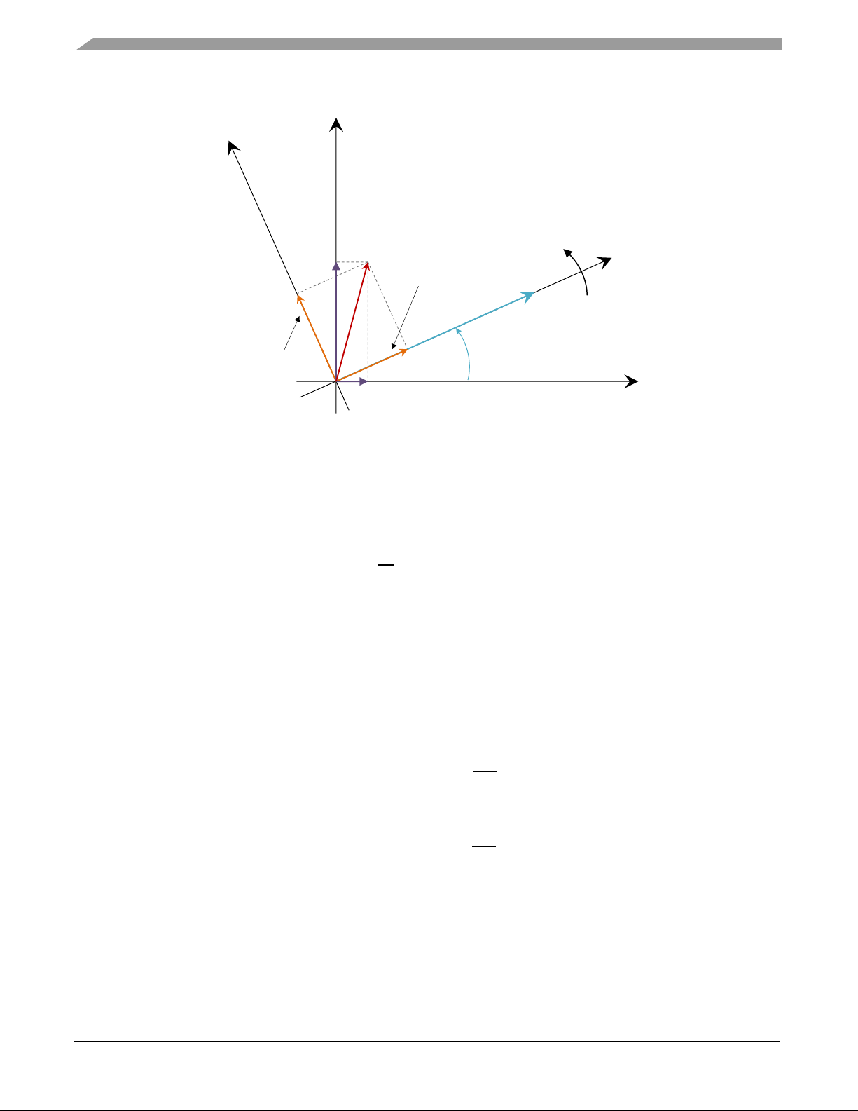
Figure 3 Orientation of stator (stationary) and rotor (rotational) reference frames, with current
components transformed into both frames
The voltage equation of the quadrature phase synchronous reference frame model can be obtained by
transforming the three phase voltage equations (Equation 2) and flux equations (Equation 3) into a two
phase rotational frame which is aligned and rotates synchronously with the rotor as shown in Figure 3.
Such transformation, after some mathematical corrections, yields the following set of equations:
Equation 4
where ωe is electrical rotor speed. It can be seen that Equation 4
represents a non-linear cross dependent system with cross-coupling terms in both d and q axis and back-
EMF voltage component in the q-axis. When FOC concept is employed, both cross-coupling terms shall
be compensated in order to allow independent control of current d and q components. Design of the
controllers is then governed by following pair of equations, derived from Equation 4 after
compensation:
Equation 5
Equation 6
Those equations describe the model of the plant for d and q current loop. Both equations are structurally
identical, therefore the same approach of controller design can be adopted for both d and q controllers.
The only difference is in values of d and q axis inductances, which results in different gains of the
controllers. Considering closed loop feedback control of a plant model as in either equation, using
α
β
d
q
ω
e
αβ frame – stator coordinates
dq frame – rotor coordinates
θ
e
i
S
i
Sd
i
Sq
i
Sα
i
Sβ
torque
component
flux
component
PM
Page 7
PMSM field-oriented control
MCSPTR2A5775E 3-phase PMSM Motor Control Kit with MPC5775E, Rev. 0, 10/2020
NXP Semiconductors 7
standard PI controllers, then the controller proportional and integral gains can be derived, using a poleplacement method, as follows:
Equation 7
Equation 8
where ω0 represents the system natural frequency [rad/sec] and ξ is the Damping factor [-] of the current
control loop.
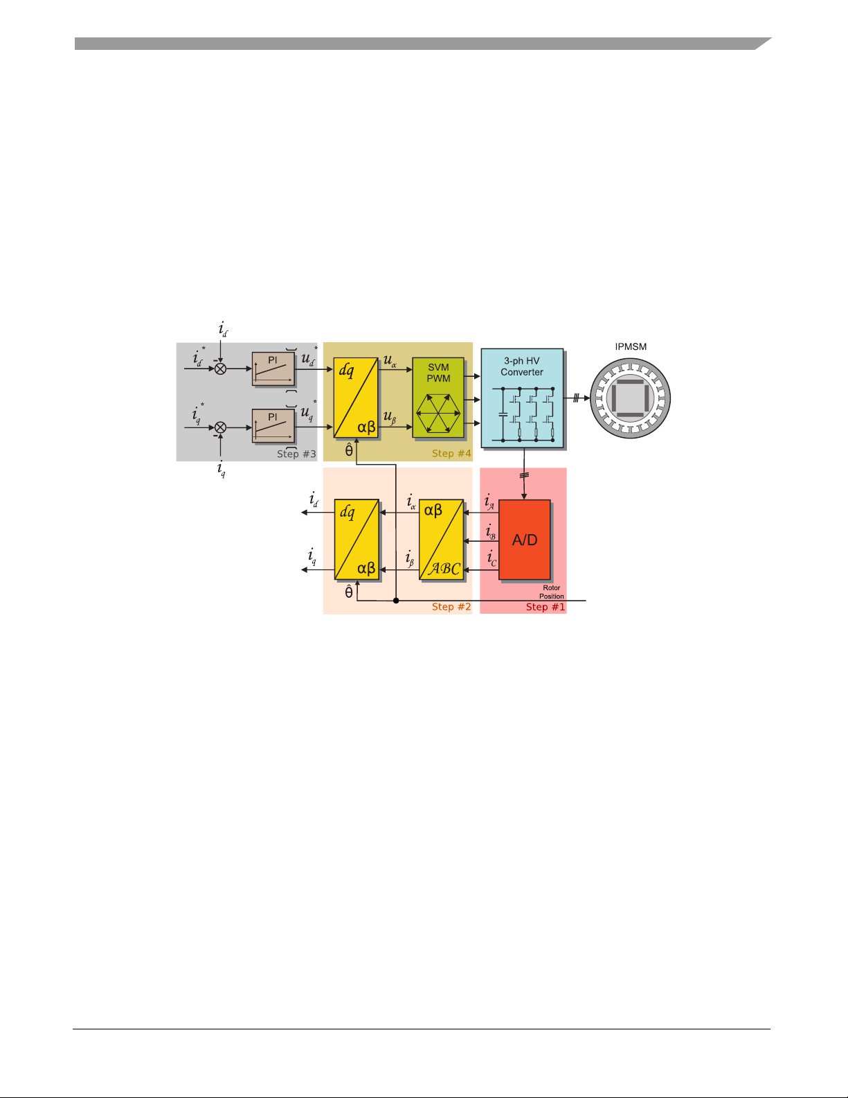
Figure 4 FOC Control Structure
3.3.
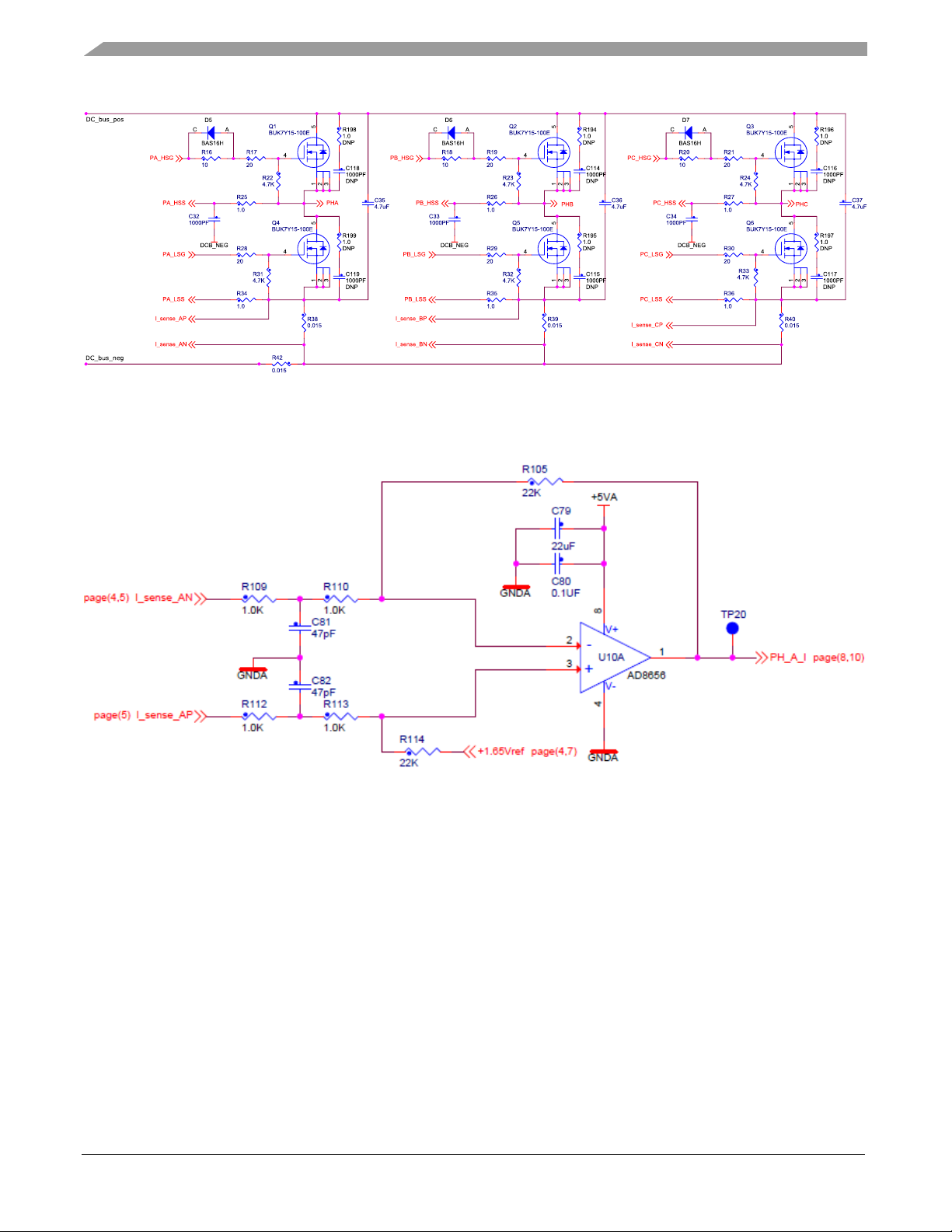
Output voltage actuation and phase current measurement
The 3-phase voltage source inverter shown in Figure 5 uses three shunt resistors (R38, R39, R40) placed
in three legs of the inverter as phase current sensors. Stator phase current which flows through the shunt
resistor produces a voltage drop which is interfaced to the AD converter of microcontroller through
conditional circuitry (refer to MCSPTR2A5775E Schematic available at nxp.com).
Page 8
PMSM field-oriented control
MCSPTR2A5775E 3-phase PMSM Motor Control Kit with MPC5775E, Rev. 0, 10/2020
8 NXP Semiconductors
Figure 5 Three-phase DC/AC inverter with shunt resistors for current measurement
Figure 6 shows a gain setup and input signal filtering circuit for operational amplifier which provides the
conditional circuitry and adjusts voltages to fit into the ADC input voltage range.
Figure 6 Phase current measurement conditional circuitry
The phase current sampling technique is a challenging task for detection of phase current differences
and for acquiring full three phase information of stator current by its reconstruction. Phase currents
flowing through shunt resistors produces a voltage drops which need to be appropriately sampled by the
AD converter when low-side transistors are switched on. The currents cannot be measured by the shunt
resistors at an arbitrary moment. This is because the current only flows through the shunt resistor when
the bottom transistor of the respective inverter leg is switched on. Therefore, considering Figure 5, phase
A current is measured using the R38 shunt resistor and can only be sampled when the low side transistor
Q4 is switched on. Correspondingly, the current in phase B has to be measured when the low side
transistor Q5 is switched on, and the current in phase C can only be measured if the low side transistor
Q6 is switched on. To get an actual instant of current sensing, voltage waveform analysis has to be
performed.
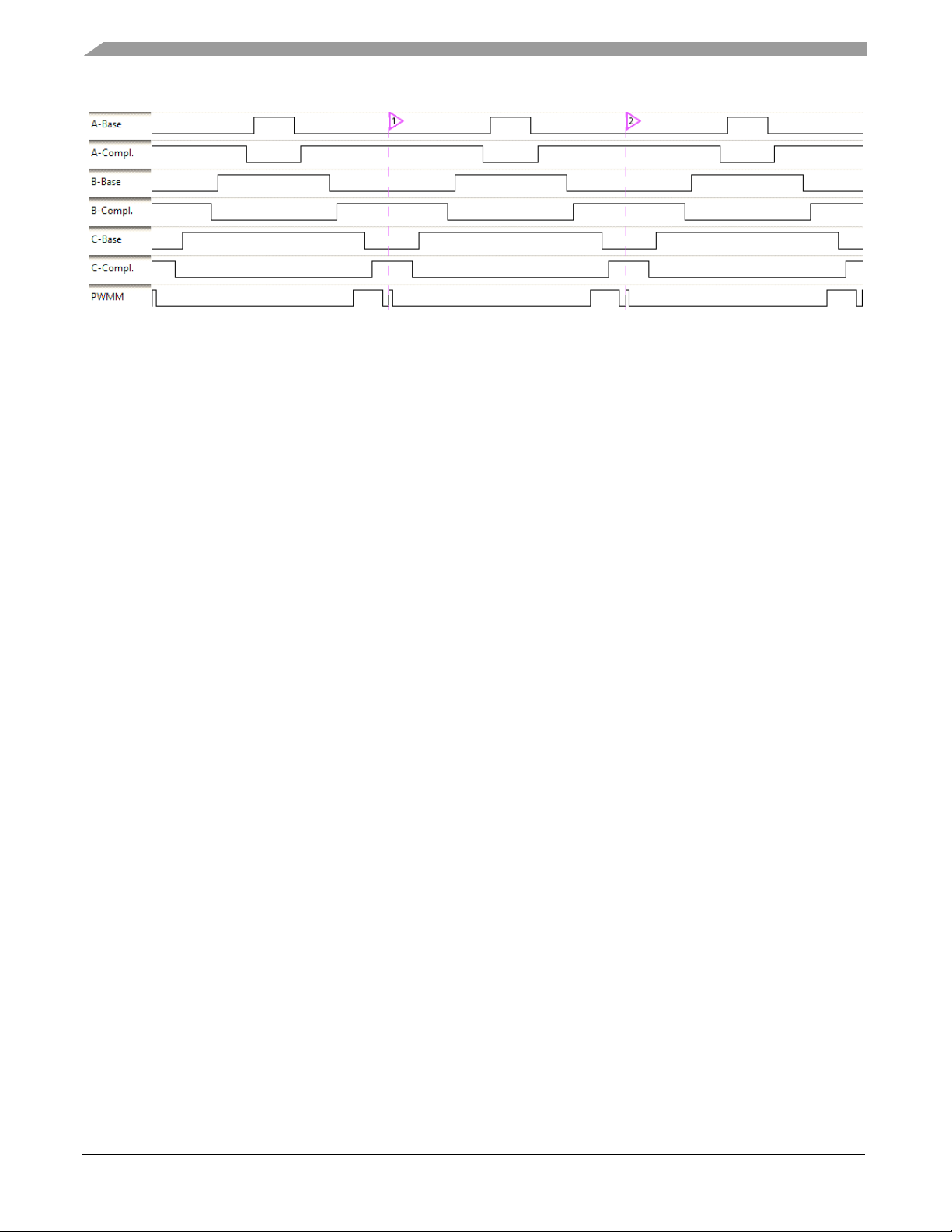
Generated duty cycles (phase A, phase B, phase C) for two consecutive PWM periods are shown in
Figure 7. These phase voltage waveforms correspond to a center-aligned PWM with sine-wave
modulation. As shown in the following figure, (PWM period I), the best sampling instant of phase
Page 9
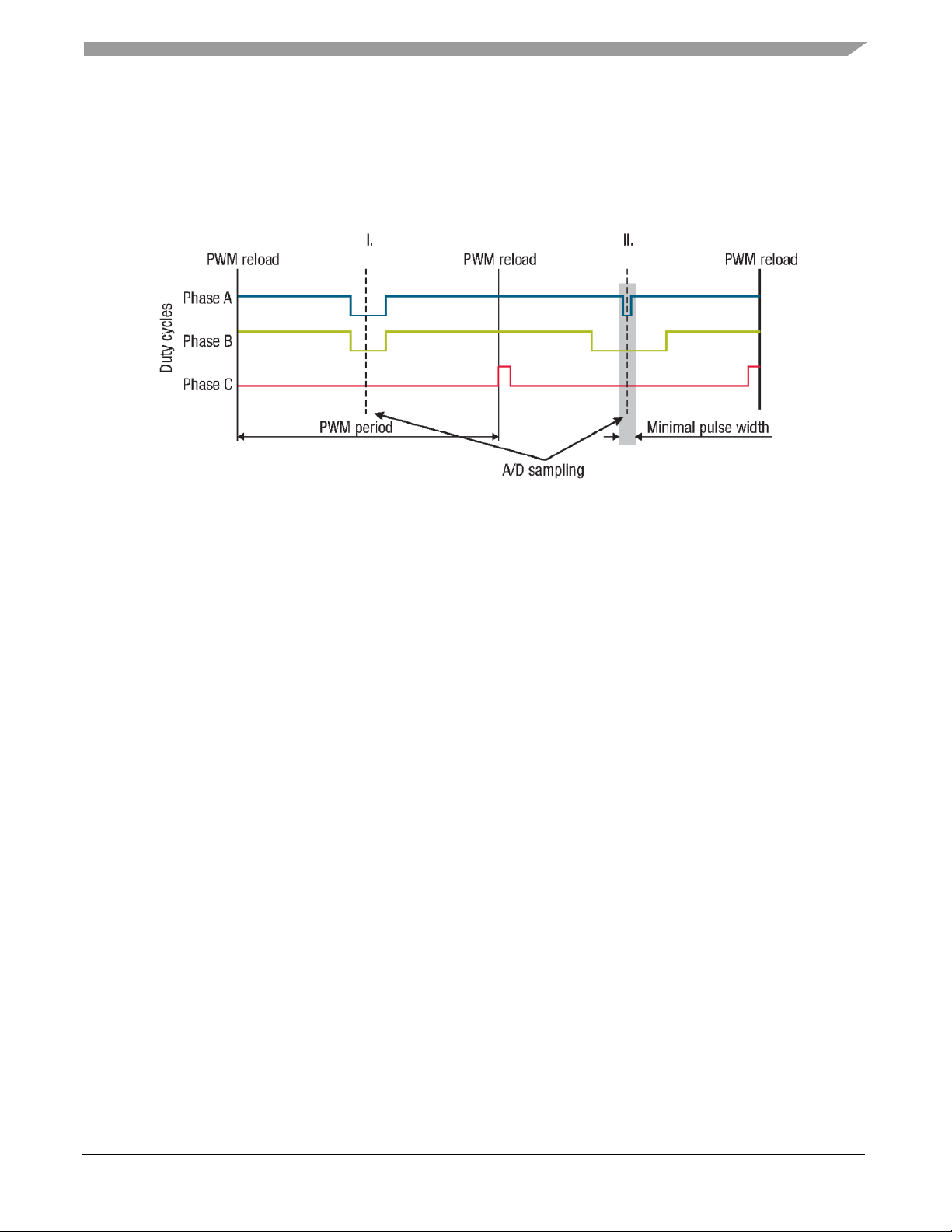
PMSM field-oriented control
MCSPTR2A5775E 3-phase PMSM Motor Control Kit with MPC5775E, Rev. 0, 10/2020
NXP Semiconductors 9
current is in the middle of the PWM period, where all bottom transistors are switched on. However, not
all three currents can be measured at an arbitrary voltage shape. PWM period II in the following figure
shows the case when the bottom transistor of phase A is ON for a very short time. If the ON time is
shorter than a certain critical time (depends on hardware design), the current cannot be correctly
measured.
Figure 7 Generated phase duty cycles in different PWM periods
In standard motor operation, where the supplied voltage is generated using the space vector modulation,
the sampling instant of phase current takes place in the middle of the PWM period in which all bottom
transistors are switched on. If the duty cycle goes to 100%, there is an instant when one of the bottom
transistors is switched on for a very short time period. Therefore, only two currents are measured and the
third one is calculated from equation:
Equation 9
NOTE
MPC5775-EVB is using eTPU timer for generation the PWMs signals.
The default limit of the PWM duty cycle is 98% which allows in whole
range of duty cycle measure all three currents. This default setting and
also type of motor control modulation can be changed. Refer to eTPU
PWMM: Center-aligned PWM mode
3.4.
Rotor position/speed estimation
Different sensor type might require different approach to evaluate the speed and position of the motor.
The NXP approach for resolver systems utilizes an Angle Tracking Observer (ATO), see Figure 8 which
is based on the Phase Lock Loop technique. The ATO input is a position error between the position
given by the sensor and estimated ATO position. The PI controller in the ATO loop minimizes the input
error by adjustment of a control variable, in this case the control variable is equivalent to a motor speed.
Integration of the speed leads to the estimated position.
Page 10

PMSM field-oriented control
MCSPTR2A5775E 3-phase PMSM Motor Control Kit with MPC5775E, Rev. 0, 10/2020
10 NXP Semiconductors
Figure 8 ATO for Resolver systems
The ATO for resolver system is characterized by the position error calculation. The observer error
corresponds to the following formula:
Equation 10
The coefficients of ATO PI controller, Integrator and filter can be tuned by MCAT tool. The ATO
function is a member of the motor control SW library (see References) and is available as
AMCLIB_TrackObsrv.
The alignment algorithm applies DC voltage to d-axis resulting full DC voltage applied to phase A and
negative half of the DC voltage applied to phase B, C for a certain period. This will cause the rotor to
move to "align" position, where stator and rotor fluxes are aligned. The rotor position in which the rotor
stabilizes after applying DC voltage is set as zero position. Motor is ready to produce full startup torque
once the rotor is properly aligned.
NOTE
MPC5775E-EVB is using eTPU for resolver feedback signal
demodulation. eTPU based resolver o digital converter is described in
chapter Software implementation on the MPC5777E.
3.5.
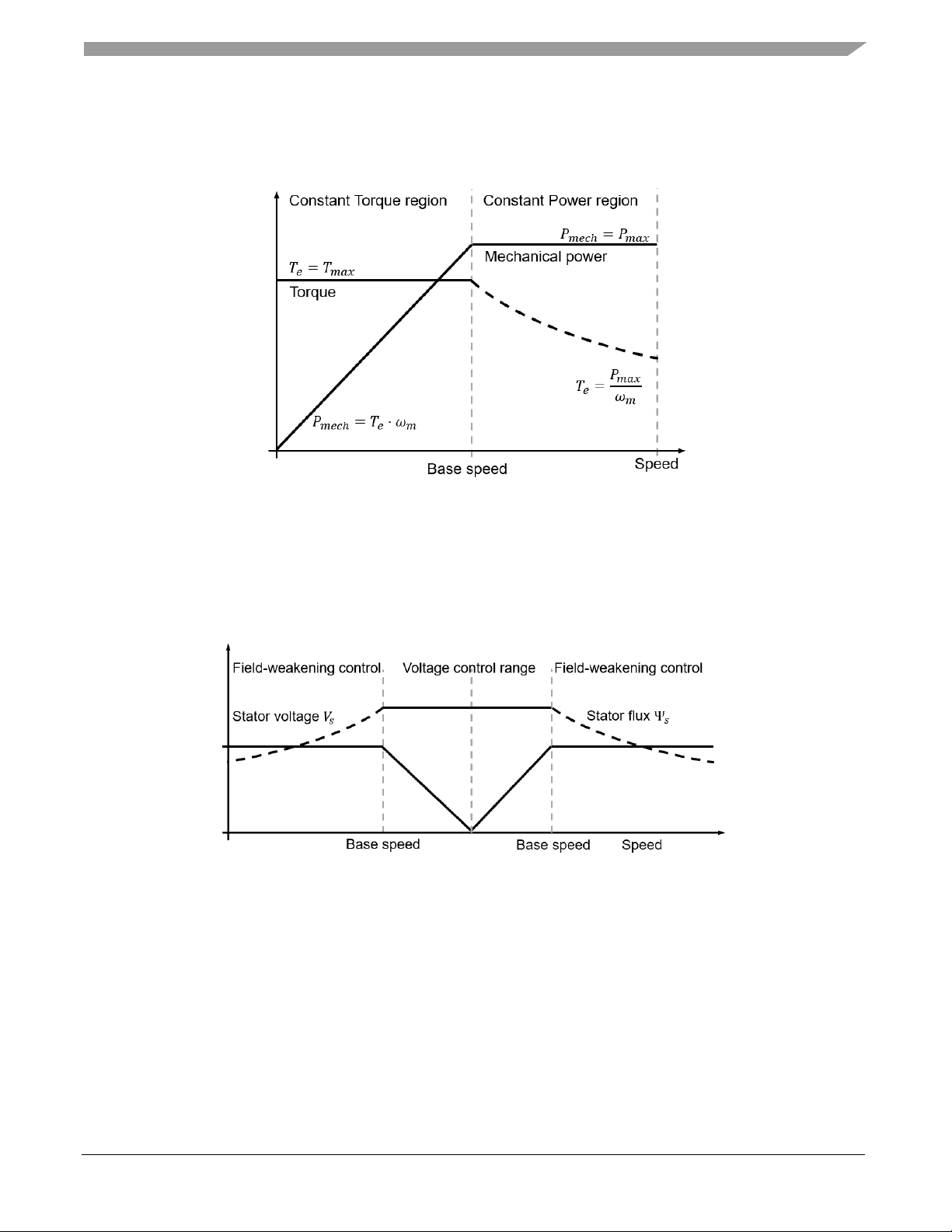
Field weakening
Field weakening is an advanced control approach that extends standard FOC to allow electric motor
operation beyond a base speed. The back electromotive force (EMF) is proportional to the rotor speed
and counteracts the motor supply voltage. If a given speed is to be reached, the terminal voltage must be
increased to match the increased stator back-EMF. A sufficient voltage is available from the inverter in
the operation up to the base speed. Beyond the base speed, motor voltages ud and uq are limited and
cannot be increased because of the ceiling voltage given by inverter. Base speed defines the rotor speed
at which the back-EMF reaches maximal value and motor still produces the maximal torque.
As the difference between the induced back-EMF and the supply voltage decreases, the phase current
flow is limited, hence the currents id and iq cannot be controlled sufficiently. Further increase of speed
would eventually result in back-EMF voltage equal to the limited stator voltage, which means a
complete loss of current control. The only way to retain the current control even beyond the base speed
is to lower the generated back-EMF by weakening the flux that links the stator winding. Base speed
Page 11
PMSM field-oriented control
MCSPTR2A5775E 3-phase PMSM Motor Control Kit with MPC5775E, Rev. 0, 10/2020
NXP Semiconductors 11
splits the whole speed motor operation into two regions: constant torque and constant power, see the
following figure.
Figure 9 Constant torque/power operating regions
Operation in constant torque region means that maximal torque can be constantly developed while the
output power increases with the rotor speed. The phase voltage increases linearly with the speed and the
current is controlled towards its reference. The operation in constant power region is characterized by a
rapid decrease in developed torque while the output power remains constant. The phase voltage is at its
limit while the stator flux decreases proportionally with the rotor speed, see the following figure.
Figure 10 Constant flux/voltage operational regions
FOC splits phase currents into the q-axis torque component and d-axis flux component. The flux current
component Id is used to weaken the stator magnetic flux linkage ΨS. Reduced stator flux ΨS yields to
lower Back-EMF and condition of Field Weakening is met. More details can be seen from the following
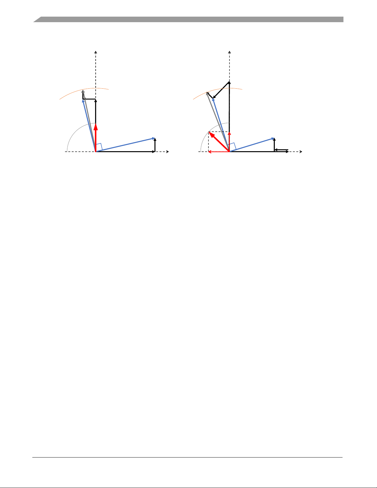
phasor diagrams of the PMSM motor operated exposing FOC control without (left) and with FW (right),
Figure 11.
Page 12
PMSM field-oriented control
MCSPTR2A5775E 3-phase PMSM Motor Control Kit with MPC5775E, Rev. 0, 10/2020
12 NXP Semiconductors
Figure 11 Steady-state phasor diagram of PMSM operation up to base speed (left) and above speed (right)
FOC without FW is operated demanding d-axis current component to be zero (Id=0) to excite electric
machine just by permanent magnets mounted on the rotor. This is an operation within constant torque
region (see Figure 9), since whole amount of the stator current consists of the torque producing
component Iq only (see Figure 11, left). Stator magnetic flux linkage ΨS1 is composed of rotor magnetic
flux linkage ΨPM, which represents the major contribution and small amount of the magnetic flux
linkage in q-axis LqIq produced by q-axis current component I
q
. Based on the Faraday’s law, rotor
magnetic flux linkage ΨPM and stator magnetic flux linkage ΨS1 produce back-EMF voltage
E
PM1=ωe1ΨPM
perpendicularly oriented to rotor magnetic flux ΨPM in q-axis and back EMF voltage
ES1=ω
e1ΨS1
perpendicularly oriented to stator magnetic flux ΨS1, respectively (see Figure 11, left). Both
voltages are directly proportional to the rotor speed ωe1. If the rotor speed exceeds the base speed, the
back-EMF voltage ES1=ω
e1ΨS1
approaches the limit given by VSI and Iq current cannot be controlled.
Hence, field weakening has to take place.
In FW operation, Id current is controlled to negative values to “weaken” stator flux linkage ΨS2 by -LdId
component as shown in Figure 11, right. Thanks to this field weakening approach, back-EMF voltage
induced in the stator windings ES2 is reduced below the VSI voltage capability even though E
PM2
exceeds it. Iq current can be controlled again to develop torque as demanded. Unlike the previous case,
this is an operation within constant power region (see Figure 9) where Iq current is limited due to Is
current vector size limitation (see Figure 11, right). In FW operation, stator magnetic flux linkage ΨS
consists of three components now: rotor magnetic flux linkage ΨPM, magnetic flux linkage in q-axis Ψq=
LqIq produced by q-axis current component Iq and magnetic flux linkage in d-axis Ψd= -LdId produced by
negative d-axis Id current component that counteracts to ΨPM.
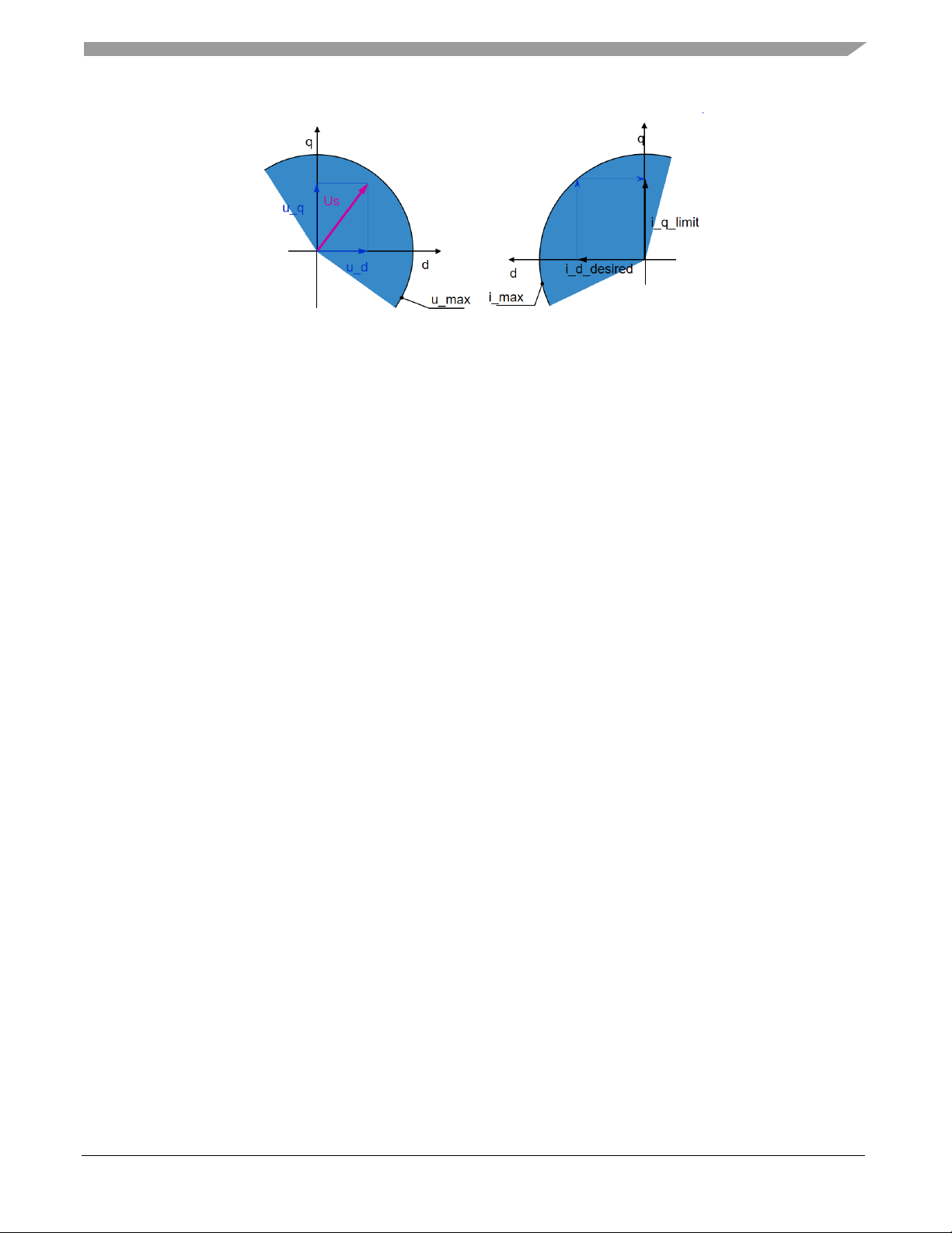
There are some limiting factors that must be taken into account when operating FOC control with field
weakening:
• Voltage amplitude u_max is limited by power as shown in Figure 12, left
• Phase current amplitude i_max is limited by capabilities of power devices and motor thermal
design as shown in Figure 12, right
• Flux linkage in d-axis is limited to prevent demagnetization of the permanent magnets
q- axis
d- axis
IS= I
q
E
PM1
=
e1
PM
V
S1
S1
RS I
S
jXSI
S
q- axis
d- axis
I
S
I
q
I
d
V
S2
S2
RS I
S
jXSI
S
-LdI
d
I
MAX
I
MAX
ES2=
e2
S2
ES1=
e1
S1
LqI
q
LqI
q
VSI voltage capability
VSI voltage capability
E
PM2
=
e2
PM
PM
PM
e1
<
e2
E
PM1
< E
PM2
Page 13
Software implementation on the MPC5777E
MCSPTR2A5775E 3-phase PMSM Motor Control Kit with MPC5775E, Rev. 0, 10/2020
NXP Semiconductors 13
Figure 12 Voltage (left) and current (right) limits for PMSM drive operation
NXP’s Automotive Math and Motor Control library offers a software solution for the FOC with field
weakening respecting all limitations discussed above. This library-based function is discussed in section
AMMCLIB integration.
4. Software implementation on the MPC5777E
4.1.
eTPU
The Enhanced Time Processing Unit (eTPU) is a programmable I/O controller with its own core and
memory system, allowing it to perform complex timing and I/O management independently of the CPU.
The eTPU is used as a co-processor, specialized for advanced timing functions, such as handle complex
engine control, motor control, and communication tasks independently of the CPU.
A new complex library of eTPU functions enabling the eTPU to drive motor control applications was
developed. This library represents a step forward compared to its predecessor – the motor control
function sets (set3 and set4). The new Motor Control eTPU Library benefits from NXP eTPU
development tools from CodeWarrior. The eTPU(2) Development Suite is based on Eclipse IDE and
includes the C and assembly compiler, simulator and debugger.
4.1.1.
eTPU PWMM:
The Motor Control PWM eTPU function (PWMM) uses either three eTPU channels to generate three
PWM output signals, or six eTPU channels to generate three complementary PWM output signal pairs,
used to drive a 3-phase electrical motor. One extra channel PWMM Master is used to synchronize all the
outputs and is responsible for all the necessary calculation. Master channel does not generate any
PWMM output, but the output is used for debugging and visualization of PWMM function processing.
An example of eTPU PWMM function can be seen on Figure 13.
Page 14
Software implementation on the MPC5777E
MCSPTR2A5775E 3-phase PMSM Motor Control Kit with MPC5775E, Rev. 0, 10/2020
14 NXP Semiconductors
Figure 13 Center aligned 3 phase PWM output with complementary channels and one Master channel
(PWMM).
Features:
• Generates three phases of PWM signals to drive an electrical motor.
• Based on the selected phase type, either single PWM outputs or complementary PWM pairs with
dead-time are generated for each motor phase.
• The PWM polarity can be separately configured for the base and the complementary PWM
outputs.
• The synchronous update of all PWM phases can happen either once or twice per PWM period:
o Frame update
o Frame and Center update (half-cycle update)
• The PWMM inputs are transformed into PWM output duty-cycles by a selected modulation. It
can be one of:
o Unsigned voltages
o Signed voltages
o Standard Space Vector Modulation
o Space Vector Modulation With O
000
Nulls
o Space Vector Modulation With O
111
Nulls
o Inverse Clark Transformation
o Sine Table Modulation
• There are four PWM modes supported. Switching between the PWM modes in run-time is also
supported:
o Left-aligned
o Right-aligned
o Center-aligned
o Inverted center-aligned
• The PWM period can be changed in run-time. The new period value is always applied at frame
update only, not at the center update.
Page 15
Software implementation on the MPC5777E
MCSPTR2A5775E 3-phase PMSM Motor Control Kit with MPC5775E, Rev. 0, 10/2020
NXP Semiconductors 15
• Generation of short pulses can be limited by a minimum pulse width – a threshold for pulse
deletion.
4.1.2.
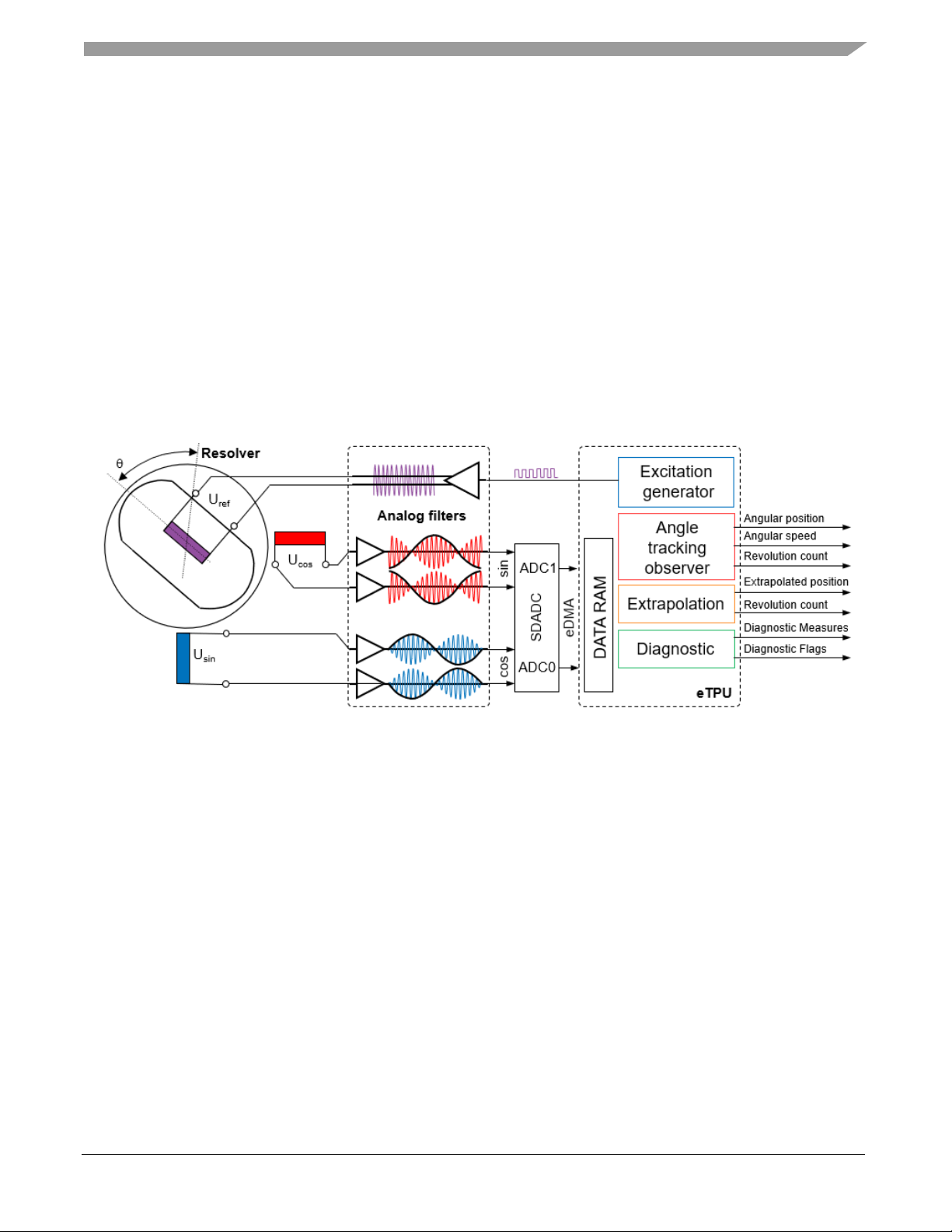
eTPU based Resolver to digital converter (RDC)
The Resolver Digital Interface eTPU function (RESOLVER) uses one eTPU channel to generate a 50%
duty-cycle PWM output signal to be passed through an external low-pass filter and used as a resolver
excitation signal. In the resolver position sensor, this excitation signal is modulated by sine and cosine of
the actual motor angle. The feedback Sine and Cosine signals are sampled by an on-chip ADC and the
conversion results can be transferred to eTPU DATA RAM by eDMA. Then, the eTPU function
RESOLVER can process the digital samples of resolver output signals. Motor angular position, angular
speed, a revolution counter, and diagnostics are results of the Sine and Cosine feedback signal
processing (see the following figure).
Figure 14 eTPU Resolver Digital Interface block diagram
Processing of the feedback signals is executed on a separate channel. Another channel is used to perform
linear extrapolation of the last updated position from ATO to any other time. This is important feature
since ATO updates come with a certain period (~50 µs) which most likely is not aligned with control
loop frequency.
Optionally, another eTPU channel can be used to process diagnostics either on the same eTPU engine
after the feedback signal processing is finished or on the other eTPU engine in parallel to the motor
angle and speed calculation. This enables the CPU application to read the new motor angle and, at the
same time, check the diagnostic results to ensure the motor angle is correct.
The Sine and Cosine analogue feedback signals need to be converted to a digital representation and
transferred to eTPU data RAM. This should be done independently of the CPU using an on-chip ADC
and eDMA. Although any of the ADC modules can be used, the described configuration adopts the
Sigma-Delta ADC (SDADC).
Page 16

Software implementation on the MPC5777E
MCSPTR2A5775E 3-phase PMSM Motor Control Kit with MPC5775E, Rev. 0, 10/2020
16 NXP Semiconductors
Two SDADC modules are used to continuously sample the Sine and Cosine signals in parallel (Figure
15). They are configured to obtain 32 samples of each signal per period instead of one sample at the
presumed peak as it is implemented in most of the SW resolver applications. This oversampling method
together with demodulation and filtration brings more robustness towards the induced noise.
Furthermore, the position is evaluated twice per resolver excitation period.
Figure 15 Oversampling and demodulation of Resolver feedback signals
4.1.3.
eTPU Analog Sensing function (AS)
The Analog Sensing eTPU function (AS) uses one eTPU channel to generate adjustable ADC trigger
pulses. On the selected eTPU channels the trigger signal generated by the AS function can be internally
routed to an ADC module. Using eDMA, the A/D conversion results can be moved back to the eTPU
data RAM for further processing by the AS eTPU function. Those pre-processed analog samples are
then available for consequential processing by e.g. an eTPU function handling the closed loop motor
control. It can run either independently with a given period (periodic mode) or it can be synchronized
with any other eTPU function (synchronized mode).
Features:
• Generates one or two adjustable trigger pulses per period:
o Frame pulse
o Center pulse
• Generates interrupts, DMA requests and eTPU links at none, one, or more of selected time-
positions:
o Frame pulse start
o Frame pulse end
Page 17

Software implementation on the MPC5777E
MCSPTR2A5775E 3-phase PMSM Motor Control Kit with MPC5775E, Rev. 0, 10/2020
NXP Semiconductors 17
o Center pulse start
o Center pulse end
• Pre-process a defined number of analog signals (ADC conversion results) using:
o Gain
o DC-offset
o Forgetting factor (low-pass EWMA filter).
• Supports processing phase currents – calculation of one phase current value using the other two-
phase current values, based on a SVM sector value.
• When working with eQADC (MPC5777C/MPC5775E), supports CPU-independent modification
of command queues.
4.2.
MPC5777E – Key modules for PMSM FOC control
The key module for motor control on MPC5775E device is Enhanced Time Processing Unit (eTPU).
Using the eTPU Motor control library function set this programmable timer co-processor is capable of
generation 3 phase PWM complementary output, analog signal measurement triggering and
synchronization signal as well as Resolver feedback signal processing. To enable full eTPU Resolver
functionality it is crucial to utilize sigma-delta Analog to digital converters together with Enhanced
Direct Memory Access module. For phase current sensing the Enhanced Queued Analog to Digital
Converters are used.
Figure 16 shows module interconnection for a typical PMSM FOC application working in sensor-based
mode using shunt current sensing with eTPU Motor Control Library functions involvement.
Figure 16 MPC5775E module interconnection block diagram
Page 18

Software implementation on the MPC5777E
MCSPTR2A5775E 3-phase PMSM Motor Control Kit with MPC5775E, Rev. 0, 10/2020
18 NXP Semiconductors
4.2.1.
MPC5777E and FETs pre-driver interconnection
Excitation of power FETs is ensured by NXP MC33937 pre-driver. This analog device is equipped with
charge pump that ensures external FETs drive at low power supply voltages. Moreover, three external
bootstrap capacitors provide gate charge to the high-side FETs (see section References).
Configuration of MC33937 pre-driver is realized via SPI module. The MC33937 allows different
operating modes to be set and locked by SPI commands. SPI commands also report condition of the
MC33937 based on the internal monitoring circuits and fault detection logic. MPC5775E detects fault
state of the MC33937 by means of fault signal MC33937 pins. Integrated current sensing amplifier with
analog comparator allow to measure DC bus current and detect overcurrent. Interconnection between
MC33937 and MPC5775E is briefly depicted in Figure 16.
4.2.2.
Module involvement in PMSM FOC control
This section will discuss timing and modules synchronization to accomplish PMSM FOC on the
MPC5775E and the internal hardware features.
The time diagram of the automatic synchronization between PWM and ADC in the PMSM application
is shown in Figure 17.
Figure 17 Time Diagram of PWM and ADC Synchronization
The PMSM FOC control with shunt current measurement is based on static timing; meaning the trigger
point instances of the ADC conversions are located at same place within one control loop cycle.
Page 19

Software implementation on the MPC5777E
MCSPTR2A5775E 3-phase PMSM Motor Control Kit with MPC5775E, Rev. 0, 10/2020
NXP Semiconductors 19
Each control cycle starts at beginning of the PWM cycle as shown in Figure 17. PWMM function runs
with a certain period that corresponds to control loop frequency. AS function is configured to run in
sync with PWMM and generates trigger pulse at the beginning of the PWMM period. This pulse rising
edge triggers eQADCs to sample phase currents and DC bus voltage. Phase currents are measured
simultaneously when bottom transistors of both inverter legs are closed, and currents flow through shunt
resistors. The rising edge of the pulse triggers also Resolver position sampling. The pulse width is
configurable and is configured for 4 µs. The falling edge of the AS pulse triggers an IRQ where the FOC
is calculated. Result of the FOC calculation is new duty cycles that has to be applied for next period. In
order to apply the new updated duty cycles for the next period the update (new duty cycle inputs) has to
come before so called “update time”. This is the time configured in PWMM function that is needed for
applying duty cycles by eTPU PWMM function for the next period, see Figure 18. If new inputs come
after the “update time” happens, then new inputs are not applied for next period and will be applied in
second next period. In that case PWMM function does not stop outputting the PWM signal and
continues with the last duty cycle values configured. Missing update IRQ is generated from eTPU
PWMM Master channel in case no new input comes before update time threshold.
Figure 18 PWMM update input values for frame update
4.3.
MPC5775E Device initialization
To simplify and accelerate application development, embedded part of the PMSM motor control
application has been created. Peripherals are initialized at beginning of the main() function. For each
MPC5775E module there is a specific configuration function:
• mcu_mode_clock_init() – MCU clock configuration
• xcptn_xmpl() – MCU interrupt routine initialization
• my_interrupt_init() – custom application interrupt initialization
• esci_init() – eSCI initialization for UART
• SIU_init() – PINs and PORT modules configuration
• my_system_etpu_init() – eTPU initialization
• edma_init() – eDMA initialization
• sdadc_init() – SDADC initialization
Page 20

Software implementation on the MPC5777E
MCSPTR2A5775E 3-phase PMSM Motor Control Kit with MPC5775E, Rev. 0, 10/2020
20 NXP Semiconductors
• eqadc_init() – eQADC initialization
• dspi_init() – DSPI initialization
4.3.1.
Clock configuration
The clock architecture of MPC5775E device contains two clock domains coming from separate PLLs.
The first one is the system clock for the cores, cross-bar switch, peripheral bridges, memories, debug
logic and memory mapped portion of peripherals. The second one feeds the state machines and protocol
engines of communication and timer peripheral modules. These two clock domains can be configured to
be completely asynchronous between each other.
PLL0 module is supplied from 40 MHz external Crystal oscillator (XOSC). PLL0 circuit multiplies the
input XOSC frequency by 10 and divides by 2 for PHI output to be 200 MHz further used as eTPU
clock, SDADC clock and further divided by 2 used as peripheral clock. Second output of PLL0 PHI1 is
divided by 4 to be 50 MHz, further used as input clock for PLL1 module.
PLL1 module is used to generate 260 MHz system clock and 130 MHz platform clock. Clocking
configuration within this application is listed in Table 1.
Table 1 MCP5775E clocking configuration
clock
frequency
core_clk
260 MHz
plat_clk
130 MHz
etpu_clk
200 MHz
per_clk
100 MHz
The configuration of overall system clock is performed within function call mcu_mode_clock_init(), see
the code example below.
void mcu_mode_clock_init(void)
{
/* 0 The crystal oscillator (XOSC) is the clock source for PLL0 */
/* 1 The internal RC oscillator (IRC) is the clock source for PLL0 */
SIU.SYSDIV.B.PLL0SEL = 0;
/* Configure PLL0 Dividers from 40Mhx XOSC */
/* phi = 200 MHz */
/* phi1 = 50 MHz */
PLLDIG.PLL0DV.B.RFDPHI1 = 4;
PLLDIG.PLL0DV.B.RFDPHI = 2;
PLLDIG.PLL0DV.B.PREDIV = 1;
PLLDIG.PLL0DV.B.MFD = 10;
/* Check whether crystal is 40MHz, if not forever loop here TODO:implement error reporting */
while (!(SIU.RSR.B.XOSCHIGH)){};
/* Ensure SIU_RSR[XOSC] is 1 to confirm that XOSC is stable. */
while (!(SIU.RSR.B.XOSC)){};
PLLDIG.PLL0CR.B.CLKCFG = 3; /* Enable PLL0 by putting PLL into Normal mode */
while (!PLLDIG.PLL0SR.B.LOCK){}; /* Test PLL0 lock */
/* Select the source clock for PLL1 */
/* 0 The crystal oscillator (XOSC) is the clock source for PLL1 */
/* 1 The PHI1 output of PLL0 is the clock source for PLL1 */
SIU.SYSDIV.B.PLL1SEL = 0;
/* Configure PLL1 Dividers - 260MHz from 40Mhx XOSC */
PLLDIG.PLL1DV.B.RFDPHI = 2;
PLLDIG.PLL1DV.B.MFD = 26;
PLLDIG.PLL1CR.B.CLKCFG = 3; /* Enable PLL1 by putting PLL into Normal mode */
while (!PLLDIG.PLL1SR.B.LOCK){}; /* Test PLL1 lock */
…
}
Page 21

Software implementation on the MPC5777E
MCSPTR2A5775E 3-phase PMSM Motor Control Kit with MPC5775E, Rev. 0, 10/2020
NXP Semiconductors 21
4.3.2.
eSCI configuration
Enhanced Serial Communication Interface (eSCI) module is used for communication between the
MPC5775E MCU and FREEMASTER runtime debugging and visualization tool. Function esci_init()
configures module A for UART functionality with baud rate 115200. See the following code example.
/* Initialize eSCI for UART */
esci_init(ESCIA_MODULE,MODE_SCI);
void esci_init(uint8_t module, uint8_t mode)
{
switch(module){
case ESCIA_MODULE:
eSCI_A.LCR1.B.LIN = mode; /* Select between LIN or SCI functionality */
eSCI_A.CR2.R = 0x2000; /* Enable ESCI and set all bits to reset value */
eSCI_A.CR1.B.TE = 1; /* Transmitter enable */
eSCI_A.CR1.B.RE = 1; /* Receiver enable */
eSCI_A.CR1.B.PT = 0; /* Parity is even */
eSCI_A.CR1.B.PE = 0; /* Parity control disable */
eSCI_A.BRR.B.SBR = 54; /* Baud rate = 115200:
MCLK = (200MHz/2), Txclk = MCLK/(16*SBR) */
break;
…
}
}
4.3.3.
eTPU configuration
eTPU function configuration is performed within so called GCT files (etpu_gct.c/.h). First there is
performed general eTPU engine configuration for both engine A and B, then eTPU functions are
assigned to selected channels and those channels are configured for that particular eTPU functionality.
The parameters for eTPU engine configuration are held in my_etpu_config structure, see part of the
structure in the following example.
/** @brief Structure handling configuration of all global settings */
struct etpu_config_t my_etpu_config =
{
/* etpu_config.mcr - Module Configuration Register */
FS_ETPU_GLOBAL_TIMEBASE_DISABLE /* keep time-bases stopped during intialization (GTBE=0) */
| FS_ETPU_MISC_DISABLE, /* SCM operation disabled (SCMMISEN=0) */
/* etpu_config.misc - MISC Compare Register*/
FS_ETPU_MISC, /* MISC compare value from etpu_set.h */
/* etpu_config.ecr_a - Engine A Configuration Register */
FS_ETPU_ENTRY_TABLE_ADDR /* entry table base address = shifted FS_ETPU_ENTRY_TABLE from etpu_set.h */
| FS_ETPU_CHAN_FILTER_2SAMPLE /* channel filter mode = three-sample mode (CDFC=0) */
| FS_ETPU_FCSS_DIV2 /* filter clock source selection = div 2 (FSCC=0) */
| FS_ETPU_FILTER_CLOCK_DIV2 /* filter prescaler clock control = div 2 (FPSCK=0) */
| FS_ETPU_PRIORITY_PASSING_ENABLE /* scheduler priority passing is enabled (SPPDIS=0) */
| FS_ETPU_ENGINE_ENABLE, /* engine is enabled (MDIS=0) */
…
}
The entire eTPU initialization and function configuration is then performed in my_system_etpu_init()
function call. See the following example code.
int32_t my_system_etpu_init(void)
Page 22

Software implementation on the MPC5777E
MCSPTR2A5775E 3-phase PMSM Motor Control Kit with MPC5775E, Rev. 0, 10/2020
22 NXP Semiconductors
{
int32_t err_code;
/* Initialization of eTPU DATA RAM */
fs_memset32((uint32_t*)fs_etpu_data_ram_start, 0, fs_etpu_data_ram_end - fs_etpu_data_ram_start);
/* Initialization of eTPU global settings */
err_code = fs_etpu_init(
my_etpu_config,
(uint32_t *)etpu_code, sizeof(etpu_code),
(uint32_t *)etpu_globals, sizeof(etpu_globals));
if(err_code != 0) return(err_code);
#ifdef FS_ETPU_ARCHITECTURE
#if FS_ETPU_ARCHITECTURE == ETPU2
/* Initialization of additional eTPU2-only global settings */
err_code = fs_etpu2_init(
my_etpu_config,
#ifdef FS_ETPU_ENGINE_MEM_SIZE
FS_ETPU_ENGINE_MEM_SIZE);
#else
0);
#endif
if(err_code != FS_ETPU_ERROR_NONE) return(err_code);
#endif
#endif
/* Initialization of eTPU channel settings */
err_code = fs_etpu_pwmm_init(&pwmm_instance, &pwmm_config);
if(err_code != FS_ETPU_ERROR_NONE) return(err_code + (ETPU_PWMM_MASTER_CH<<16));
err_code = fs_etpu_as_init(&as_instance, &pwmm_instance, &as_config);
if(err_code != FS_ETPU_ERROR_NONE) return(err_code + (ETPU_AS_CH<<16));
err_code = fs_etpu_resolver_init(&resolver_instance, &resolver_config);
if(err_code != FS_ETPU_ERROR_NONE) return(err_code + (ETPU_RESOLVER_EXC_CHAN<<16));
return(0);
}
4.3.3.1.
eTPU PWMM: Center-aligned PWM mode
The Motor Control PWM eTPU function (PWMM) uses either three eTPU channels to generate three
PWM output signals, or six eTPU channels to generate three complementary PWM output signal pairs,
used to drive a 3-phase electrical motor.
In this application complementary pairs of PWM are used with center aligned configuration, frame
update only (parameters are updated once per PWM period, on a frame) and signed voltage modulation.
Period is configured for 100 µs, dead-time configuration is 1 µs as well as minimum pulse width.
Update time is configured for 7 µs which ensures enough time to perform update of all the three phases
for next period.
PWMM function configuration is performed within etpu_gct.c file. Part of the configuration is held in
pwmm_instance where PWMM channels are assigned, complementary channel mode, function priority
and polarity of the PWM outputs are configured. Other parameters, those that can be changed during
runtime, are held in pwmm_config structure and can be changed using fs_etpu_pwmm_config() function
call. Parameters are applied in upcoming PWMM update. The change of parameters is then visible in
next period after the PWMM update. See the timing of the updates illustrated on Figure 18.
struct pwmm_config_t pwmm_config =
{
FS_ETPU_PWMM_FM1_FRAME_UPDATE_ONLY, /**< selection of PWM update position. */
FS_ETPU_PWMM_MODULATION_SIGNED, /**< Selection of modulation */
Page 23

Software implementation on the MPC5777E
MCSPTR2A5775E 3-phase PMSM Motor Control Kit with MPC5775E, Rev. 0, 10/2020
NXP Semiconductors 23
FS_ETPU_PWMM_MODE_CENTER_ALIGNED, /**< PWM Mode selection */
NSEC2TCR1(100000), /**< PWM period as a number of TCR1 cycles. */
USEC2TCR1(1), /**< PWM dead-time as a number of TCR1 cycles.*/
USEC2TCR1(1), /**< Minimum pulse width as number of TCR1 cycles. */
USEC2TCR1(7) /**< A time period (number of TCR1 cycles) that is needed to
perform an update of all PWM phases. */
};
NOTE
Use predefined macros to configure intended functionality. All the
possible options are listed in etpu_pwmm.h in comments and described in
PWMM-doxydoc.chm file. Note that parameters in pwmm_instance can be
configured only once at the eTPU initialization and cannot be changed
during runtime.
4.3.3.2.
eTPU Resolver configuration
Resolver function is designed so it cooperates closely with SDADC modules. SDADCs are configured
to provide 32 per one period of resolver feedback signal. Having considered the resolver excitation
frequency to be 10 kHz it means 320 kHz output data rate is required for SDADC. With a given
limitations of SDADC clocking and oversampling rate configurations the closest possible output data
rate that can be configured is 320.512 kHz (see Table 2). This determines the resolver excitation
frequency to be 10.016 kHz, 99.84 µs period respectively. Resolver bandwidth configuration can be
changed modifying ATO P and I gains. Current configuration of ATO is for 1 kHz bandwidth.
Excitation P and I gains are tuned for balanced phase-shift reaction, thus it is recommended to use this
configuration. For more information about eTPU Resolver implementation and its configuration please
refer to eTPU RDC and RDC Checker User Guide (References).
struct resolver_config_t resolver_config =
{
FS_ETPU_RESOLVER_SEMAPHORE_0,
FS_ETPU_RESOLVER_OPTIONS_CALCULATION_ON +
FS_ETPU_RESOLVER_OPTIONS_DIAG_MEASURES_ON +
FS_ETPU_RESOLVER_OPTIONS_EXC_ADAPTATION_ON +
FS_ETPU_RESOLVER_OPTIONS_EXC_GENERATION_ON, /* Resolver function options */
NSEC2TCR1(99840), /* Excitation signal period */
SFRACT24(0.070597541), /* ATO P-gain */
SFRACT24(0.002492006), /* ATO I-gain */
SFRACT24(0.00000), /* Excitation P-gain */
SFRACT24(0.00012), /* Excitation I-gain */
SFRACT24(0.9) /* Speed EWMA filter coefficient */
};
4.3.3.3.
eTPU AS: triggering output pulse
AS function is capable of generation periodical trigger pulses, one or two per period: Frame and Center
pulse. The position of the pulses (relative to AS period frame time and center time) is configurable as
well as the length.
In this application AS function is configured to work in synchronization mode adopting the period of
PWMM function. In that case AS period is configured to zero and pointer to the PWMM period is
provided in etpu_as.c file. The polarity of the AS signal is configured as high for the pulse. Those
Page 24

Software implementation on the MPC5777E
MCSPTR2A5775E 3-phase PMSM Motor Control Kit with MPC5775E, Rev. 0, 10/2020
24 NXP Semiconductors
configurations are held in as_instace structure (defined similarly like PWMM in etpu_gct.c) and are not
a subject of change during the runtime. AS is configured to output one Frame pulse at the beginning of
the PWMM period (on a Frame time) and length is configured to be 4 µs which is enough for all the
feedback sampling and DMA transfer to eTPU data RAM. The AS pulse is internally gated to eQADC
to trigger conversion. AS pulse is also used to trigger Resolver Extrapolation. For this purpose there
need to be a HW connection between the eTPU AS channel output and eTPU Resolver Sample channel
input. If fulfilled rising edge of the AS pulse triggers extrapolation of the position - in other words
sampling the position and speed at the same time point as the feedback current measurement. IQR is
generated at the falling edge of the trigger pulse eTPU_AS_Isr() where all the feedback values are
processed and state machine is executed.
Also, configuration for measured signals triggered by AS function is present in etpu_gct.c in structure
called as_signal_config. This structure holds one sub-configuration structure per signal, number of the
signals to be processed by AS is defined in as_instance at the AS function initialization. The signal
configuration structure holds parameters like gain, DC offset and filter factor. The processing of the
signals may and may not be used. Within this application the processing of feedback signals is
performed by CPU, not eTPU AS function.
The following example code with AS configuration and AS signal configuration structures.
/** A structure to represent a single AS signal processing configuration.
* It includes both static and dynamic values. */
struct as_signal_config_t as_signal_config[4] =
{
{
0, /* Result queue offset of the signal */
1, /* Gain bit */
0x2000, /* DC offset */
SFRACT24(0) /* Forget factor of the EWMA filter */
},
…
};
/** A structure to represent a configuration of AS.
* It includes AS configuration items which can mostly be changed in
* run-time. */
struct as_config_t as_config =
{
0, /* Start offset */
0, /* Period */
USEC2TCR1(4), /* Pulse width */
FS_ETPU_AS_FM0_FRAME_PULSE_ON, /* Pulse selection */
0, /* Frame pulse adjustment */
0, /* Center pulse adjustment */
FS_ETPU_AS_IRQ_FRAME_PULSE_END, /* IRQ and DMA options */
0, /* Link options */
0, /* Link channels numbers at frame pulse start */
0, /* Link channels numbers at frame pulse end */
0, /* Link channels numbers at center pulse start */
0, /* Link channels numbers at center pulse end */
(uint32_t *)(0xC3FC8000 + 0x1000), /* Pointer to eTPU data RAM where signals from ADC are stored */
&as_signal_config[0], /* Pointer to a signal configuration structure */
0xF, /* Mask determining signals to be processed at frame pulse end */
0x0, /* Mask determining signals to be processed at center pulse end */
FS_ETPU_AS_PHASE_CURRENTS_OFF, /* Phase current processing option */
0, /* Phase A current index in result queue */
1, /* Phase B current index in result queue */
2, /* Phase C current index in result queue */
…
};
Page 25

Software implementation on the MPC5777E
MCSPTR2A5775E 3-phase PMSM Motor Control Kit with MPC5775E, Rev. 0, 10/2020
NXP Semiconductors 25
4.3.4.
SDADC configuration
The Sine and Cosine analog feedback signals need to be converted to a digital representation and
transferred to eTPU data RAM for Resolver function processing. This should be done independently of
the CPU using an on-chip ADC and eDMA. Although any of the ADC modules can be used, the
described configuration adopts the Sigma-Delta ADC (SDADC).
Two SDADC modules are used to continuously sample the Sine and Cosine signals in parallel. They are
configured to obtain 32 samples of each signal per period. The following table details the configuration
for a 10 kHz excitation signal and a 320 kHz sampling frequency.
Table 2 SDADC configuration for Resolver
Configuration Item
Value
SDADC clock
200 MHz / 13 = 15.38 MHz (available range 4 – 16 MHz)
ADC decimation rate
24
Resulting output data rate
200 MHz / 13 / (2 * 24) = 320,512.8 Hz
Input mode
Single-ended
High-pass filter
enabled
FIFO size
16 words
FIFO threshold
8 words
DMA request on FIFO full
selected and enabled
NOTE
In this application single-ended mode is configured for SDADC to sense
resolver feedback signals (sine and cosine). This results from the Low
voltage power stage circuitry allowing single ended measurement for
position feedback. However, it is recommended to use differential
configuration for SDADC (and of course corresponding circuitry) when
using SDADCs for eTPU Resolver signal digitization. This brings the
advantage of noise rejection.
Using the function call sdadc_init() two instances of SDADC, namely SDADC1 and SDADC4 are
configured for continuous sampling with a given output data rate as listed in Table 2.
SDADC1 is started by software. SDADC1 trigger output is selected as a HW trigger to start SDADC4.
This configuration enables to start both modules of SDADC synchronously. Both SDADC modules are
configured so they generate DMA request as soon as FIFO sample count reaches the value 8. It means
that quarter of sine wave is moved by DMA from SDADC result FIFO to eTPU data RAM at once, four
times per period. See the following code example.
/* SDADC init*/
sdadc_init(OSR_24, GAIN_1, FTHLD_8, SINGLE);
void sdadc_init(uint8_t pdr, uint8_t gain, uint8_t fifo_thld, uint8_t inp_mode)
{
/* SD ADC 1 CONFIGURATION */
SDADC_1.SFR.R = 0x1B; /* Clear all the status flags */
SDADC_1.FCR.B.FRST = 1; /* Generate reset to flush FIFO */
SDADC_1.FCR.B.FTHLD = fifo_thld; /* FIFO threshold - overcome generates FIFO full event flag */
Page 26

Software implementation on the MPC5777E
MCSPTR2A5775E 3-phase PMSM Motor Control Kit with MPC5775E, Rev. 0, 10/2020
26 NXP Semiconductors
SDADC_1.FCR.B.FSIZE = 3; /* FIFO size: 0 - 1 word, 1 - 4 words, 2 - 8 words, 3 - 16 words */
SDADC_1.FCR.B.FOWEN = 0; /* Disable FIFO overwrite */
SDADC_1.FCR.B.FE = 1; /* Enable FIFO */
SDADC_1.RSER.B.DFFDIRS = 1; /* DMA request on data FIFO full */
SDADC_1.RSER.B.DFFDIRE = 1; /* Data FIFO full request enable */
SDADC_1.MCR.B.MODE = inp_mode; /* Input mode: 0 - differential, 1 - single-ended */
SDADC_1.MCR.B.PDR = pdr; /* Over sampling rate */
SDADC_1.MCR.B.PGAN = gain; /* Digital gain */
SDADC_1.MCR.B.HPFEN = 1; /* High-pass filter enabled */
SDADC_1.MCR.B.EN = 1; /* Internal SDADC modulator enabled */
SDADC_1.OSDR.B.OSD = 1; /* Set the output settling delay */
SDADC_1.CSR.B.ANCHSEL = 0; /* Analog input channel AN[x] selection */
SDADC_1.MCR.B.TRIGEN = 1; /* Enable HW trigger */
…
SDADC_4.MCR.B.TRIGSEL = 0; /* SDADC_1 trigger output selected as an input trigger for SDADC4 */
SDADC_4.MCR.B.TRIGEDSEL = 1; /* Rising edge of trigger input selected */
SDADC_4.MCR.B.TRIGEN = 1; /* Enable HW trigger */
}
void sdadc_start(void)
{
/* start the SDADC_1 by SW trigger */
SDADC_1.STKR.R = 0xFFFF;
}
4.3.5.
eQADC configuration
MPC5775E features two instances of Enhanced Queued ADCs (eQADC), each module having two
independent ADCs, total four independent on-chip ADC modules. The eQADC transfers commands
from multiple Command FIFOs (CFIFOs) to the on-chip ADCs. The multiple Result FIFOs (RFIFOs)
can receive data from the on-chip ADCs or from an on-chip DSP module. The eQADC supports
software and external hardware triggers from other blocks to initiate transfers of commands from the
CFIFOs to the on-chip ADCs. It also monitors the fullness of CFIFOs and RFIFOs, and accordingly
generates DMA or interrupt requests to control data movement between the FIFOs and the system
memory, which is external to the EQADC.
In this application all the four on-chip ADCs are utilized to sample simultaneously Phase A, Phase B
and Phase C currents and DC bus voltage. This is achieved by utilizing of four command FIFOs, one per
ADC channel. External HW trigger is configured to trigger CFIFOs, namely eTPUA_28 channel is
selected as a trigger input for all CFIFOs. This eTPU channel is assigned to AS function. ADCs are
configured for single scan mode. Results are stored in Result FIFOs, one RFIFO per ADC channel.
FIFO Drain DMA requests are enabled for all the CFIFOs as well as RFIFOs. On a CFIFO Drain DMA
request respective eQADC command is transferred from system memory to CFIFO. Commands for all
the channels have the end Of Queue bit (EOQ) configured. This results in repeated write of a single
command to the CFIFO after CFIFO is triggered. Result FIFO drain DMA request evokes respective
DMA channel that performs transfer from RFIFO to eTPU data RAM. See the configuration of the
DMA channels in Table 5 and Table 6. See the following code example of the EQADC initialization.
void eqadc_init(void)
{
uint32_t tmp;
/* AN24 - Phase A current
* AN25 - Phase B current
* AN26 - Phase C current
* AN28 - DC bus voltage */
Page 27

Software implementation on the MPC5777E
MCSPTR2A5775E 3-phase PMSM Motor Control Kit with MPC5775E, Rev. 0, 10/2020
NXP Semiconductors 27
/* SIU config of CFIFO trigger source selection:
* eTPU28_A selected to trigger all the FIFOs at one time */
SIU.ISEL5.B.CTSEL0_A = 0xC; /* eTPU28_A selected as trigger for eQADC_A Command FIFO 0 */
SIU.ISEL5.B.CTSEL1_A = 0xC; /* eTPU28_A selected as trigger for eQADC_A Command FIFO 1 */
SIU.ISEL7.B.CTSEL0_B = 0xC; /* eTPU28_A selected as trigger for eQADC_B Command FIFO 0 */
SIU.ISEL7.B.CTSEL1_B = 0xC; /* eTPU28_A selected as trigger for eQADC_B Command FIFO 1 */
/* Enable EQADC_A ADC0 and ADC1 and set ADC clock prescaler, via commands */
EQADC_A.CFCR0.B.CFINV0 = 1; /* invalidate CFIFO */
EQADC_A.CFCR0.B.CFINV1 = 1; /* invalidate CFIFO */
EQADC_A.CFPR[0].R = 0x80800301 + (0 << 25); /* push ADC0_CR configuration command to CFIFO_0 */
EQADC_A.CFPR[1].R = 0x80800301 + (1 << 25); /* push ADC1_CR configuration command to CFIFO_1 */
EQADC_A.CFCR0.R = 0x04100410; /* set software triggered single scan mode and enable single scan for both
ADC0 and ADC1 */
while (EQADC_A.FISR[0].B.EOQFX != 1) {} /* wait for end-of-queue flag */
while (EQADC_A.FISR[1].B.EOQFX != 1) {} /* wait for end-of-queue flag */
EQADC_A.FISR[0].R = ~0UL; /* clear all flags */
EQADC_A.FISR[1].R = ~0UL; /* clear all flags */
}
4.3.6.
DSPI configuration
DSPI module is used as a communication interface between MPC5775E MCU and FET pre-driver
MC33937. DSPI B module is configured for that purpose within this application using function call
dspi_init(). DSPI is configured as master mode SPI interface with 6.25 MHz frequency derived from
100 MHz PER_CLK. See the following configuration code.
/* DSPI initialization */
dspi_init(DSPI_B_MODULE, DSPI_MASTER, DSPI_SPI, CTAR0);
void dspi_init(uint8_t module, uint8_t mode, uint8_t com_mode, uint8_t ctar)
{
switch(module){
…
case DSPI_B_MODULE:
DSPI_B.MCR.B.HALT = 0x1; /* Module is set to HALT mode to perform initialization */
DSPI_B.MCR.B.MDIS = 0x1; /* Module is disabled during initialization */
DSPI_B.MCR.B.MSTR = mode; /* Select module mode: MASTER or SLAVE */
DSPI_B.MCR.B.PCSIS = 0x3F; /* The chip select inactive state is high */
DSPI_B.MCR.B.DIS_RXF = 0x1; /* RX FIFO disabled */
DSPI_B.MCR.B.DIS_TXF = 0x1; /* TX FIFO disabled */
DSPI_B.MCR.B.CLR_TXF = 0x1; /* Clear the TX FIFO counter */
DSPI_B.MCR.B.CLR_RXF = 0x1; /* Clear the RX FIFO counter */
DSPI_B.MODE.CTAR[ctar].B.FMSZ = 0x7; /* Frame size is FRMSZ + 1 = 8bit per frame */
DSPI_B.MODE.CTAR[ctar].B.DBR = 0x0; /* Duty cycle of the SCK is 50/50 */
DSPI_B.MODE.CTAR[ctar].B.CPOL = 0x0; /* Clock polarity: inactive state value of SCK is low */
DSPI_B.MODE.CTAR[ctar].B.CPHA = 0x1; /* Clock phase: Data is changed on leading edge of SCK */
DSPI_B.MODE.CTAR[ctar].B.LSBFE = 0x0; /* LSB first: Data is transferred MSB first */
DSPI_B.MODE.CTAR[ctar].B.CSSCK = 0x3; /* PCS to SCK Delay Scaler set to 16 */
DSPI_B.MODE.CTAR[ctar].B.ASC = 0x3; /* After SCK Delay Scaler set to 16 */
DSPI_B.MODE.CTAR[ctar].B.DT = 0x7; /* Delay After Transfer Scaler set to 128 */
DSPI_B.MODE.CTAR[ctar].B.BR = 0x3; /* Baud rate scaler is set to be 8, resultant DSPI clock
is 100 MHZ/(2x8) = 6.25 MHz */
DSPI_B.RSER.R = 0x0; /* No interrupts or DMA transfers enabled */
break;
…
}
}
Page 28

Software implementation on the MPC5777E
MCSPTR2A5775E 3-phase PMSM Motor Control Kit with MPC5775E, Rev. 0, 10/2020
28 NXP Semiconductors
DSPI routines are used within MC33937.c/.h driver. Also PIT timer is utilized here for timing. With all
of this MC33937 driver provides access to all features of MC33937 FET driver chip such as
reading/writing status registers, dead-time configuration and fault handling. See the following example
code.
tBool MC33937_configure( MC33937_T *ptr)
{
volatile uint8_t cnt;
uint8_t empty_data;
uint16_t command;
volatile tBool statusPass;
statusPass = TRUE;
statusPass &= ClearRESET();
statusPass &= ClearEN();
statusPass &= SetRESET();
/* start the PIT to count 2 ms */
pit_start_wait_ns(2000000);
while(!pit_read_flag());
pit_stop();
/* initiate the DSPI */
statusPass &= dspi_start();
/* Clear all faults */
statusPass &= MC33937_clear_faults(ptr);
/* Initialize MASK register 0 */
command = (uint16_t)ptr->data.mc33937mask0;
statusPass &= dspi_master_data_tx(SINGLE_CS,CS3,CTAR0, command, &empty_data);
…
}
4.3.7.
DMA transfer configuration
Within this application eleven DMA channels are utilized to speed up the control loop operation and
offload the CPU. DMA is used to transfer:
• Samples of Resolver feedback sine and cosine signals from SDADC to eTPU data RAM
• eQADC commands to command FIFO for phase current and DC bus voltage measurement
• eQADC measurement from result FIFO to eTPU data RAM
All the channels used in this application are listed in the following table together with respective DMA
request sources.
Table 3 eDMA channel usage in application
Module
DMA chan.
Requesting source
Description
eDMA A
0
EQADC_A_FISR0[CFFF0]
EQADC_A Command FIFO 0 Fill Flag (Phase A current
measurement commands)
1
EQADC_A_FISR0[RFDF0]
EQADC_A Receive FIFO 0 Drain Flag (Phase A current values)
2
EQADC_A_FISR1[CFFF1]
EQADC_A Command FIFO 1 Fill Flag (Phase B current
measurement commands)
3
EQADC_A_FISR1[RFDF1]
EQADC_A Receive FIFO 1 Drain Flag (Phase B current values)
eDMA B
0
EQADC_B_FISR0[CFFF0]
EQADC_B Command FIFO 0 Fill Flag (Phase C current
measurement commands)
1
EQADC_B_FISR0[RFDF0]
EQADC_B Receive FIFO 0 Drain Flag (Phase C current values)
2
EQADC_B_FISR1[CFFF1]
EQADC_B Command FIFO 1 Fill Flag (DC bus voltage
measurement commands)
3
EQADC_B_FISR1[RFDF1]
EQADC_B Receive FIFO 1 Drain Flag (DC bus voltage values)
36
SDADC0
SDADC_0 result ready (sine positive resolver feedback signal)
Page 29

Software implementation on the MPC5777E
MCSPTR2A5775E 3-phase PMSM Motor Control Kit with MPC5775E, Rev. 0, 10/2020
NXP Semiconductors 29
Module
DMA chan.
Requesting source
Description
39
SDADC3
SDADC_3 result ready (cosine positive resolver feedback signal)
48 - This channel is linked by eDMA B 36
NOTE
The numbering of SDADC instances differs in MPC5775E Reference
manual in various chapters. SDADC instances are numbered 1-4 whereas
the source signals from SDADCs to trigger eDMA operation are
numbered 0-3. Note that eDMA trigger signal SDADC_0 result ready
originates in SDADC1 module and similarly SDADC_3 result ready
originates in SDADC4 module.
For the purpose of eTPU Resolver function operation three eDMA channels are used to ensure Resolver
feedback signals are delivered to eTPU data RAM and to trigger eTPU processing once all the data are
transferred. Two eDMA B channels 36 and 39 are configured to transfer SDADC results after SDADC
result FIFO count reaches 8. Channel 36 is configured to link another eDMA B channel (channel 48) on
major loop completion (after all the results are transferred into eTPU data RAM) which causes a
subsequent transfer of constants into eTPU Resolver ATO channel HSR register. The array of the
constants defined in edma.c source file and is as follows:
const uint32_t link_cnst[] = {0,
FS_ETPU_RESOLVER_HSR_UPDATE_1ST,
0,
FS_ETPU_RESOLVER_HSR_UPDATE_2ND};
It means that after first quarter of sine wave samples is transferred into eTPU data RAM zero is written
into Resolver ATO eTPU channel HSR register. Writing a zero does not initiate any eTPU operation. On
the second quarter transfer end the FS_ETPU_RESOLVER_HSR_UPDATE_1
ST
constant is written to HSR register. This
write initiates eTPU service request for processing first half period of the sampled sine and cosine wave.
Similar applies for the second half period with FS_ETPU_RESOLVER_HSR_UPDATE_2
ND
that evokes processing of the
second half period. Detailed configuration for DMA channels used by eTPU Resolver function can be
found in Table 4.
Table 4 DMA configuration for eTPU Resolver
Configuration Item
Sine ADC FIFO DMA
channel
Cosine ADC FIFO DMA
channel
Linked HSR DMA channel
Source address
&SDADC_x.CDR.R
&SDADC_y.CDR.R
&link_const[0]
Destination address
resolver_instance.
.signals_pba
resolver_instance.
.signals_pba + 64
&ETPU.CHAN[resolver_instanc
e.chan_num_exc].HSRR.R
Source transfer size / modulo
32-bits / 0 bytes
32-bits / 0 bytes
32-bits / 0 bytes
Destination transfer size /
modulo
32-bits / 0 bytes
32-bits / 0 bytes
32-bits / 0 bytes
Source address offset
0 bytes
0 bytes
4 bytes
Destination address offset
4 bytes
4 bytes
0 bytes
Minor loop byte count
32 bytes
32 bytes
4 bytes
Major loop iteration count
4 4 4
Last source address adjustment
0 bytes
0 bytes
-16 bytes
Page 30

Software implementation on the MPC5777E
MCSPTR2A5775E 3-phase PMSM Motor Control Kit with MPC5775E, Rev. 0, 10/2020
30 NXP Semiconductors
Configuration Item
Sine ADC FIFO DMA
channel
Cosine ADC FIFO DMA
channel
Linked HSR DMA channel
Source address
&SDADC_x.CDR.R
&SDADC_y.CDR.R
&link_const[0]
Destination address
resolver_instance.
.signals_pba
resolver_instance.
.signals_pba + 64
&ETPU.CHAN[resolver_instanc
e.chan_num_exc].HSRR.R
Source transfer size / modulo
32-bits / 0 bytes
32-bits / 0 bytes
32-bits / 0 bytes
Destination transfer size /
modulo
32-bits / 0 bytes
32-bits / 0 bytes
32-bits / 0 bytes
Source address offset
0 bytes
0 bytes
4 bytes
Last destination address
adjustment
-128 bytes
-128 bytes
0 bytes
Channel to channel linking
enabled
disabled
disabled
Linked channel
HSR DMA channel
-
-
See the code example below where the configuration of DMA_B channel 36 for transferring sine signal
samples from SDADC1 to eTPU data RAM is shown, according to Table 4.
void edma_init(void)
{
uint8_t hsr_ch = 48;
/* DMA B ch 36 - SDADC0 result ready
DMA B ch 39 - SDADC3 result ready */
/* DMA settings for SDADC_0 request */
DMA_B.TCD[36].SADDR.R = (uint32_t)&SDADC_1.CDR.R;/* Source address */
DMA_B.TCD[36].ATTR.B.SMOD = 0; /* Source address modulo*/
DMA_B.TCD[36].ATTR.B.SSIZE = 2; /* Source data size: 32bit */
DMA_B.TCD[36].ATTR.B.DMOD = 0; /* Destination address modulo */
DMA_B.TCD[36].ATTR.B.DSIZE = 2; /* Destination data size: 32bit */
DMA_B.TCD[36].SOFF.R = 0; /* Source address signed offset */
DMA_B.TCD[36].NBYTES.MLNO.R = 32; /* Inner "minor" byte count (8*4) */
DMA_B.TCD[36].SLAST.R = 0; /* TCD Last Source Address Adjustment */
DMA_B.TCD[36].DADDR.R = (vuint32_t)resolver_instance.signals_pba; /* Destination address */
DMA_B.TCD[36].CITER.ELINKYES.B.ELINK = 1; /* Enable chan-to-chan linking on minor-loop complete */
DMA_B.TCD[36].CITER.ELINKYES.B.LINKCH = hsr_ch; /* Minor Loop Link Channel Number */
DMA_B.TCD[36].CITER.ELINKYES.B.CITER = 4; /* Current major iteration count */
DMA_B.TCD[36].DOFF.R = 4; /* Signed destination address offset */
DMA_B.TCD[36].DLASTSGA.R = -128; /* Last destination address adjustment /scatter gather
address */
DMA_B.TCD[36].BITER.ELINKYES.B.ELINK = 1; /* Enable chan-to-chan linking on minor loop complete */
DMA_B.TCD[36].BITER.ELINKYES.B.LINKCH = hsr_ch; /* Minor Loop Link Channel Number */
DMA_B.TCD[36].BITER.ELINKYES.B.BITER = 4; /* Beginning major iteration count */
DMA_B.TCD[36].CSR.B.MAJORELINK = 1; /* Enable chan-to-chan linking on major loop complete */
DMA_B.TCD[36].CSR.B.MAJORLINKCH = hsr_ch; /* Major Loop Link Channel Number */
…
}
Another four eDMA channels are used to transfer eQADC commands from system memory to eQADC
command FIFO. The DMA transfer is requested when the command FIFO is empty. eQADC
commands can be seen below.
const uint32_t eqadc_commands[] =
{
0x80001800, /* Phase A: EQADC_A ADC 0, channel 24, EOQ */
0x82101900, /* Phase B: EQADC_A ADC 1, channel 25, EOQ */
0x80001A00, /* Phase C: EQADC_B ADC 0, channel 26, EOQ */
0x82101C00, /* DCB : EQADC_B ADC 1, channel 28, EOQ */
};
Page 31

Software implementation on the MPC5777E
MCSPTR2A5775E 3-phase PMSM Motor Control Kit with MPC5775E, Rev. 0, 10/2020
NXP Semiconductors 31
Detailed configuration for DMA channels used by eQADC can be found in the following table.
Table 5 eDMA configuration for eQADC command FIFO
Configuration Item
EQADC_A Command
FIFO 0 DMA channel
EQADC_A Command
FIFO 1 DMA channel
EQADC_B Command
FIFO 0 DMA channel
EQADC_B Command
FIFO 1 DMA channel
Source address
&eqadc_commands[0]
&eqadc_commands[1]
&eqadc_commands[2]
&eqadc_commands[3]
Destination address
&EQADC_A.CFPR[0].R
&EQADC_A.CFPR[1].R
&EQADC_B.CFPR[0].R
&EQADC_B.CFPR[1].R
Source transfer size /
modulo
32-bits / 0 bytes
32-bits / 0 bytes
32-bits / 0 bytes
32-bits / 0 bytes
Destination transfer size /
modulo
32-bits / 0 bytes
32-bits / 0 bytes
32-bits / 0 bytes
32-bits / 0 bytes
Source address offset
0 bytes
0 bytes
0 bytes
0 bytes
Destination address
offset
0 bytes
0 bytes
0 bytes
0 bytes
Minor loop byte count
4 bytes
4 bytes
4 bytes
4 bytes
Major loop iteration count
1 1 1
1
Last source address
adjustment
0 bytes
0 bytes
0 bytes
0 bytes
Last destination address
adjustment
0 bytes
0 bytes
0 bytes
0 bytes
Channel to channel
linking
disabled
disabled
disabled
disabled
Linked channel
- - -
-
See the code example below where the configuration of DMA_A channel 0 for transferring eQADC
commands to measure Phase A current by eQADC are transferred from system memory to eQADC
command FIFO is shown, according to Table 5.
/* DMA settings for eQADC command FIFO */
/* phaseA - DMA_A source: 0 EQADC_A Command FIFO 0 Fill Flag */
/* phaseB - DMA_A source: 2 EQADC_A Command FIFO 1 Fill Flag */
/* phaseC - DMA_B source: 0 EQADC_B Command FIFO 0 Fill Flag */
/* DCB Voltage - DMA_B source: 2 EQADC_B Command FIFO 1 Fill Flag */
DMA_A.TCD[0].SADDR.R = (uint32_t)&eqadc_commands[0];/* Source address */
DMA_A.TCD[0].ATTR.B.SMOD = 0; /* Source address modulo */
DMA_A.TCD[0].ATTR.B.SSIZE = 2; /* Source data size: 32bit */
DMA_A.TCD[0].ATTR.B.DMOD = 0; /* Destination address modulo */
DMA_A.TCD[0].ATTR.B.DSIZE = 2; /* Destination data size: 32bit */
DMA_A.TCD[0].SOFF.R = 0; /* Source address signed offset */
DMA_A.TCD[0].NBYTES.MLNO.R = 4; /* Inner "minor" byte count */
DMA_A.TCD[0].SLAST.R = 0; /* TCD Last Source Address Adjustment */
DMA_A.TCD[0].DADDR.R = (uint32_t)&EQADC_A.CFPR[0].R;/* Destination address CFIFO */
DMA_A.TCD[0].CITER.ELINKNO.B.ELINK = 0; /* Disable chan-to-chan linking on minor-loop complete */
DMA_A.TCD[0].CITER.ELINKNO.B.CITER = 1; /* Current major iteration count */
DMA_A.TCD[0].DOFF.R = 0; /* Signed destination address offset */
DMA_A.TCD[0].DLASTSGA.R = 0; /* Last destination address adjustment /scatter gather
address */
DMA_A.TCD[0].BITER.ELINKNO.B.ELINK = 0; /* Disable chan-to-chan linking on minor loop complete */
DMA_A.TCD[0].BITER.ELINKNO.B.BITER = 1; /* Beginning major iteration count */
DMA_A.TCD[0].CSR.B.MAJORELINK = 0; /* Disable chan-to-chan linking on major loop complete */
Page 32

Software implementation on the MPC5777E
MCSPTR2A5775E 3-phase PMSM Motor Control Kit with MPC5775E, Rev. 0, 10/2020
32 NXP Semiconductors
Last set of four eDMA channels are used to transfer results from eQADC Result FIFO to eTPU data
RAM for further processing. Detailed configuration for DMA channels used by eQADC result FIFO is
shown in Table 6.
Table 6 eDMA channel configuration for eQADC Result FIFO
Configuration Item
EQADC_A Receive
FIFO 0 DMA channel
EQADC_A Receive
FIFO 1 DMA channel
EQADC_B Receive
FIFO 0 DMA channel
EQADC_B Receive
FIFO 1 DMA channel
Source address
&EQADC_A.RFPR[0].R
&EQADC_A.RFPR[1].R
&EQADC_B.RFPR[0].R
&EQADC_B.RFPR[1].R
Destination address
0xC3FC9000
(free eTPU data RAM
space)
0xC3FC9004
(free eTPU data RAM
space)
0xC3FC9008
(free eTPU data RAM
space)
0xC3FC900C
(free eTPU data RAM
space)
Source transfer size /
modulo
32-bits / 0 bytes
32-bits / 0 bytes
32-bits / 0 bytes
32-bits / 0 bytes
Destination transfer size /
modulo
32-bits / 0 bytes
32-bits / 0 bytes
32-bits / 0 bytes
32-bits / 0 bytes
Source address offset
0 bytes
0 bytes
0 bytes
0 bytes
Destination address
offset
0 bytes
0 bytes
0 bytes
0 bytes
Minor loop byte count
4 bytes
4 bytes
4 bytes
4 bytes
Major loop iteration count
1 1 1
1
Last source address
adjustment
0 bytes
0 bytes
0 bytes
0 bytes
Last destination address
adjustment
0 bytes
0 bytes
0 bytes
0 bytes
Channel to channel
linking
disabled
disabled
disabled
disabled
Linked channel
- - -
-
See the code example below where the configuration of DMA_A channel 1 for transferring Phase A
current samples from eQADC to eTPU data RAM is shown, according to Table 6.
/* DMA settings for eQADC result FIFO */
/* phaseA - DMA_A source: 1 EQADC_A Receive FIFO 0 Drain Flag*/
/* phaseB - DMA_A source: 3 EQADC_A Receive FIFO 1 Drain Flag */
/* phaseC - DMA_B source: 1 EQADC_B Receive FIFO 0 Drain Flag */
/* DCB Voltage - DMA_B source: 3 EQADC_B Receive FIFO 1 Drain Flag */
DMA_A.TCD[1].SADDR.R = (uint32_t)&EQADC_A.RFPR[0].R; /* Source address */
DMA_A.TCD[1].ATTR.B.SMOD = 0; /* Source address modulo*/
DMA_A.TCD[1].ATTR.B.SSIZE = 2; /* Source data size: 32bit */
DMA_A.TCD[1].ATTR.B.DMOD = 0; /* Destination address modulo */
DMA_A.TCD[1].ATTR.B.DSIZE = 2; /* Destination data size: 32bit */
DMA_A.TCD[1].SOFF.R = 0; /* Source address signed offset */
DMA_A.TCD[1].NBYTES.MLNO.R = 4; /* Inner "minor" byte count */
DMA_A.TCD[1].SLAST.R = 0; /* TCD Last Source Address Adjustment */
DMA_A.TCD[1].DADDR.R = 0xC3FC8000 + 0x1000; /* Destination address eTPU AS signals array */
DMA_A.TCD[1].CITER.ELINKNO.B.ELINK = 0; /* Disable channel-to-channel linking on minor-loop complete */
DMA_A.TCD[1].CITER.ELINKNO.B.CITER = 1; /* Current major iteration count */
DMA_A.TCD[1].DOFF.R = 0; /* Signed destination address offset */
DMA_A.TCD[1].DLASTSGA.R = 0; /* Last destination address adjustment /scatter gather address */
DMA_A.TCD[1].BITER.ELINKNO.B.ELINK = 0; /* Disable channel-to-channel linking on minor loop complete */
DMA_A.TCD[1].BITER.ELINKNO.B.BITER = 1; /* Beginning major iteration count */
DMA_A.TCD[1].CSR.B.MAJORELINK = 0; /* Disable channel-to-channel linking on major loop complete */
Page 33

Software implementation on the MPC5777E
MCSPTR2A5775E 3-phase PMSM Motor Control Kit with MPC5775E, Rev. 0, 10/2020
NXP Semiconductors 33
4.3.8.
Port control and pin multiplexing
PMSM FOC motor control application requires following on chip pins assignment, see Table 7.
Table 7 Pins assignment for MPC5775E PMSM FOC control
Module
Signal name
Pin name / Functionality
Description
eQADC A
M_AN24
ANA24/ANB24
Phase A curent
M_AN25
ANA25/ANB25
Phase B curent
eQADC B
M_AN26
ANA26/ANB26
Phase C curent
M_AN28
ANA28/ANB28
DC Bus Voltage
SDADC 1
M_ANA0_SDA0
ANA0/SDA0
Sine positive resolver feedback signal
(single ended)
SDADC 4
M_ANB0_SDD0
ANB0/SDD0
Cosine positive resolver feedback signal
(single ended)
eSCI A
TXDA
TXDA/GPIO89
UART transmit data (FreeMASTER)
RXDA
RXDA/GPIO90
UART receive data (FreeMASTER)
DSPI B
DSPI_SCKB
SCKB/GPIO102
DSPI B Clock Output
DSPI_SINB
SINB/GPIO103
DSPI B Serial Data Input
DSPI_SOUTB
SOUTB/GPIO104
DSPI B Serial Data Output
DSPI_CSB3
PCSB3/GPIO108
DSPI B Chip select 3 Output signal for
MC33937
eTPU A
M_eTPUA0
ETPUA0 /GPIO114
PWMM Master channel
M_eTPUA6
ETPUA6 /GPIO120
Resolver Excitation output
M_eTPUA16
ETPUA16 /GPIO130
PWMM Phase A Base channel (high-side
driver)
M_eTPUA17
ETPUA17 /GPIO131
PWMM Phase A Complementary channel
(low-side driver)
M_eTPUA18
ETPUA18 /GPIO132
PWMM Phase B Base channel (high-side
driver)
M_eTPUA19
ETPUA19 /GPIO133
PWMM Phase B Complementary channel
(low-side driver)
M_eTPUA20
ETPUA20 /GPIO134
PWMM Phase C Base channel (high-side
driver)
M_eTPUA21
ETPUA21 /GPIO135
PWMM Phase C Complementary channel
(low-side driver)
eTPUA27
ETPUA27 /GPIO141
Resolver Sample (Extrapolation) input
M_eTPUA28
ETPUA28 /GPIO142
Analog Sensing trigger output
eTPU B
eTPUB8
ETPUB8 /GPIO155
Resolver ATO channel (no input/output)
GPIO
M_eTPUA12
ETPUA12/GPIO126
Enable signal for MC33937
M_eTPUA13
ETPUA13/GPIO127
Reset signal for MC33937
M_IRQ12
IRQ12/GPIO138
Interrupt signal indicating MC33937 fault
M_IRQ3
IRQ3/GPIO453
Application control UP button
M_IRQ4
IRQ4/GPIO454
Application control DOWN button
M_IRQ11
IRQ11/GPIO137
Application switch
M_eTPUA15
GPIO129
Connecting / disconnecting braking resistor
Pin configuration listed in Table 7 is performed within SIU_init() function call.
NOTE
Pins with PWM functionality are first configured as GPIO outputs within
SIU_init() function call and outputs are configured for high side and low
side initial setup. This is needed for MC33937 configuration. After the
MC33937 configuration is finished within MCAT_Init() function call the
Page 34

Software implementation on the MPC5777E
MCSPTR2A5775E 3-phase PMSM Motor Control Kit with MPC5775E, Rev. 0, 10/2020
34 NXP Semiconductors
SIU_PWM_pin_config() routine is called that configures pins with
intended PWM functionality for respective eTPU PWMM channels. See
the code below.
void SIU_init(void)
{
…
/* configure GPIO functionality for HS and LS toggle on PWM pins */
SIU.PCR[130].B.PA = 0; /* GPIO[130] - PWM PHA base */
SIU.PCR[130].B.OBE = 1; /* Output buffer enable */
SIU.PCR[131].B.PA = 0; /* GPIO[131] - PWM PHA complementary */
SIU.PCR[131].B.OBE = 1; /* Output buffer enable */
SIU.PCR[132].B.PA = 0; /* GPIO[132] - PWM PHB base */
SIU.PCR[132].B.OBE = 1; /* Output buffer enable */
SIU.PCR[133].B.PA = 0; /* GPIO[133] - PWM PHB complementary */
SIU.PCR[133].B.OBE = 1; /* Output buffer enable */
SIU.PCR[134].B.PA = 0; /* GPIO[134] - PWM PHC base */
SIU.PCR[134].B.OBE = 1; /* Output buffer enable */
SIU.PCR[135].B.PA = 0; /* GPIO[135] - PWM PHC complementary */
SIU.PCR[135].B.OBE = 1; /* Output buffer enable */
/* High side initial setup */
SIU.GPDO[130].R = 0;
SIU.GPDO[132].R = 0;
SIU.GPDO[134].R = 0;
/* Low side initial setup */
SIU.GPDO[131].R = 1;
SIU.GPDO[133].R = 1;
SIU.GPDO[135].R = 1;
…
}
void SIU_PWM_pin_config(void)
{
/* Configure pins for eTPU functionality */
SIU.PCR[130].B.PA = 1; /* eTPUA16 - PWM PHA base */
SIU.PCR[130].B.OBE = 1; /* Output buffer enable */
SIU.PCR[131].B.PA = 1; /* eTPUA17 - PWM PHA complementary */
SIU.PCR[131].B.OBE = 1; /* Output buffer enable */
SIU.PCR[132].B.PA = 1; /* eTPUA18 - PWM PHB base */
SIU.PCR[132].B.OBE = 1; /* Output buffer enable */
SIU.PCR[133].B.PA = 1; /* eTPUA19 - PWM PHB complementary */
SIU.PCR[133].B.OBE = 1; /* Output buffer enable */
SIU.PCR[134].B.PA = 1; /* eTPUA20 - PWM PHC base */
SIU.PCR[134].B.OBE = 1; /* Output buffer enable */
SIU.PCR[135].B.PA = 1; /* eTPUA21 - PWM PHC complementary */
SIU.PCR[135].B.OBE = 1; /* Output buffer enable */
}
4.4.
Software architecture
4.4.1.
Introduction
This section describes the software design of the PMSM Field Oriented Control framework application.
The application overview and description of software implementation are provided. The aim of this
chapter is to help in understanding of the designed software.
Page 35

Software implementation on the MPC5777E
MCSPTR2A5775E 3-phase PMSM Motor Control Kit with MPC5775E, Rev. 0, 10/2020
NXP Semiconductors 35
4.4.2.
Application data flow overview
The application software is interrupt driven running in real time. There is one periodic interrupt
service routine associated with the eTPU analog sensing interrupt, executing all motor control tasks.
This includes both fast current and slow speed loop control. All tasks are performed in an order
described by the application state machine shown in Figure 21, and application flowcharts shown in
Figure 19 and Figure 20.
Figure 19 Flow chart diagram of main function with background loop
To achieve precise and deterministic sampling of analog quantities and to execute all necessary motor
control calculations, the state machine functions are called within a periodic interrupt service routine.
Hence, in order to call state machine functions, the peripheral causing this periodic interrupt must be
properly configured and the interrupt enabled. As described in section MPC5775E Device initialization,
all peripherals are initially configured and all interrupts are enabled after a RESET of the device. As
soon as interrupts are enabled and all MPC5775E peripherals are correctly configured, the state machine
functions are called from the eTPU analog sensing interrupt service routine. The background loop
handles non-critical timing tasks, such as the FreeMASTER communication polling.
Page 36

Software implementation on the MPC5777E
MCSPTR2A5775E 3-phase PMSM Motor Control Kit with MPC5775E, Rev. 0, 10/2020
36 NXP Semiconductors
Figure 20 Flow chart diagram of periodic interrupt service routine.
4.4.3.
State machine
The application state machine is implemented using a two-dimensional array of pointers to the functions
using variable called StateTable[Event][State](). The first parameter describes the current application
event, and the second parameter describes the actual application state. These two parameters select a
particular pointer to state machine function, which causes a function call whenever
StateTable[Event][State]() is called.
Page 37

Software implementation on the MPC5777E
MCSPTR2A5775E 3-phase PMSM Motor Control Kit with MPC5775E, Rev. 0, 10/2020
NXP Semiconductors 37
Figure 21 Application state machine
The application state machine consists of following six states, which are selected using variable state
defined as:
AppStates:
• INIT - state = 0
• FAULT - state = 1
• READY - state = 2
• CALIB - state = 3
• ALIGN - state = 4
• RUN - state = 5
Page 38

Software implementation on the MPC5777E
MCSPTR2A5775E 3-phase PMSM Motor Control Kit with MPC5775E, Rev. 0, 10/2020
38 NXP Semiconductors
To signalize/initiate a change of state, eleven events are defined, and are selected using variable event
defined as:
AppEvents:
• e_fault - event = 0
• e_fault_clear - event = 1
• e_init - event = 2
• e_init_done - event = 3
• e_ready - event = 4
• e_app_on - event = 5
• e_app_off - event = 11
• e_calib - event = 6
• e_calib_done - event = 7
• e_align - event = 8
• e_align_done - event = 9
• e_run - event = 10
4.4.3.1.
State – FAULT
The application goes immediately to this state when a fault is detected. The system allows all states to
pass into the FAULT state by setting cntrState.event = e_fault. State FAULT is a state that transitions
back to itself if the fault is still present in the system and the user does not request clearing of fault flags.
There are two different variables to signal fault occurrence in the application. The warning register
tempFaults represents the current state of the fault pin/variable to warn the user that the system is getting
close to its critical operation. And the fault register permFaults represents a fault flag, which is set and
put the application immediately to fault state. Even if fault source disappears, the fault remains set until
manually cleared by the user. Such mechanisms allow for stopping the application and analyzing the
cause of failure, even if the fault was caused by a short glitch on monitored pins/variables. State FAULT
can only be left when application variable switchFaultClear is manually set to true (using
FreeMASTER) or by simultaneously pressing the user buttons (BTN0 and BTN1) on the
MCSPTR2A5775E inverter board. That is, the user has acknowledged that the fault source has been
removed and the application can be restarted. When the user sets switchFaultClear = true; the following
sequence is automatically executed, see the following code.
FAULT
e_fault
e_fault_clear
e_fault
Figure 22 FAULT state with transitions
Page 39

Software implementation on the MPC5777E
MCSPTR2A5775E 3-phase PMSM Motor Control Kit with MPC5775E, Rev. 0, 10/2020
NXP Semiconductors 39
if (cntrState.usrControl.switchFaultClear)
{
// Clear permanent and temporary SW faults
permFaults.mcu.R = 0; // Clear mcu faults
permFaults.motor.R = 0; // Clear motor faults
permFaults.stateMachine.R = 0; // Clear state machine faults
MC33937Status.B.MC33937ClearErr = true; // Clear MC33937 faults
// When all Faults cleared prepare for transition to next state.
cntrState.usrControl.readFault = true;
cntrState.usrControl.switchFaultClear = false;
cntrState.event = e_fault_clear;
}
Setting event to cntrState.event = e_fault_clear while in FAULT state represents a new request to
proceed to INIT state. This request is purely user action and does not depend on actual fault status. In
other words, it is up to the user to decide when to set switchFaultClear true. However, according to the
interrupt data flow diagram shown in Figure 20, function faultDetection() is called before state machine
function state_table[event][state](). Therefore, all faults will be checked again and if there is any fault
condition remaining in the system, the respective bits in permFaults and tempFaults variables will be
set. As a consequence of permFaults not equal to zero, function faultDetection() will modify the
application event from e_fault_clear back to e_fault, which means jump to fault state when state
machine function state_table[event][state]() is called. Hence, INIT state will not be entered even though
the user tried to clear the fault flags using switchFaultClear. When the next state (INIT) is entered, all
fault bits are cleared, which means no fault is detected (permFaults = 0x0) and application variable
switchFaultClear is manually set to true.
The application is scanning for following system warnings and errors:
• DC bus over voltage
• DC bus under voltage
• DC bus over current
• Phase A and phase B over current
The thresholds for fault detection can be modified in INIT state. Please see chapter MCAT settings and
tuning for further information on how to set these thresholds using the MCAT. In addition, fault state is
entered if following errors are detected:
Page 40

Software implementation on the MPC5777E
MCSPTR2A5775E 3-phase PMSM Motor Control Kit with MPC5775E, Rev. 0, 10/2020
40 NXP Semiconductors
• PDB Errors (PDB Sequence error)
• MC33937 pre-driver errors (overtemperature, desaturation fault, low supply voltage, DC bus
overcurrent, phase error, framing error, write error after block, existing reset). See section
References.
• FOC Error (irrelevant event call in state machine or Back-EMF failure)
4.4.3.2.
State – INIT
Figure 23 INIT state with transitions
State INIT is "one pass" state/function, and can be entered from all states except for READY state,
provided there are no faults detected. All application state variables are initialized in state INIT. After
the execution of INIT state, the application event is automatically set to cntrState.event=e_init_done,
and state READY is selected as the next state to enter.
Figure 24 Flow chart of state INIT
4.4.3.3.
State – READY
Figure 25 READY state with transitions
In READY state, application is waiting for user command to start the motor. The application is released
from waiting mode by pressing the on board button BTN0 or BTN1 or by FreeMASTER interface
setting the variable switchAppOnOff = true (see flow chart in Figure 26).
INIT
e_init
e_init_done
e_app_off
READY
e_init_done
e_app_on
e_ready
Page 41

Software implementation on the MPC5777E
MCSPTR2A5775E 3-phase PMSM Motor Control Kit with MPC5775E, Rev. 0, 10/2020
NXP Semiconductors 41
Figure 26 Flow chart of state READY
4.4.3.4.
State – CALIB
Figure 27 CALIB state with transitions
Once the state machine enters CALIB state, all PWM outputs are enabled. State calib is reserved for
ADC modules calibration. MCSPTR2A5775E provides eTPU based motor control. All analogue
quantitnies are sampled and post processed by eTPU. Calibration, offset calibration and filtering are part
of analog sensing function from eTPU function selector.
State CALIB is a state that allows transition back to itself, provided no faults are present, the user does
not request stop of the application (by switchAppOnOff=true), and the calibration process has not
finished. When application event is automatically set to cntrState.event=e_calib_done, state machine
can proceed to state ALIGN.
A transition to FAULT state is performed automatically when a fault occurs. A transition to INIT state is
performed by setting the event to cntrState.event=e_app_off, which is done automatically on falling
edge of switchAppOnOff=false using FreeMASTER.
CALIB
e_app_on
e_app_off
e_calib_done
e_calib
Page 42

Software implementation on the MPC5777E
MCSPTR2A5775E 3-phase PMSM Motor Control Kit with MPC5775E, Rev. 0, 10/2020
42 NXP Semiconductors
4.4.3.5.
State – ALIGN
Figure 28 ALIGN state with transitions
This state shows alignment of the rotor and stator flux vectors to mark zero position. When using a
model-based approach for position estimation, the zero position is not known. The zero position is
obtained at ALIGN state, where a DC voltage is applied to d-axis voltage for a certain period. This will
cause the rotor to rotate to "align" position, where stator and rotor fluxes are aligned. The rotor position
in which the rotor stabilizes after applying this DC voltage is set as zero position. In order to wait for
rotor to stabilize in an aligned position, a certain time period is selected during which the DC voltage is
constantly applied. The period of time and the amplitude of DC voltage can be modified in INIT state.
Timing is implemented using a software counter that counts from a pre-defined value down to zero.
During this time, the event remains set to cntrState.event=e_align. When the counter reaches zero, the
counter is reset back to the pre-defined value, and event is automatically set to
cntrState.event=e_align_done. This enables a transition to RUN state see flow chart in Figure 29.
ALIGN
e_app_off
e_align_done
e_calib_done
e_align
Page 43

Software implementation on the MPC5777E
MCSPTR2A5775E 3-phase PMSM Motor Control Kit with MPC5775E, Rev. 0, 10/2020
NXP Semiconductors 43
Figure 29 Flow chart of state ALIGN
A transition to FAULT state is performed automatically when a fault occurs. Transition to INIT state is
performed by setting the event to cntrState.event=e_app_off, which is done automatically on falling
edge of switchAppOnOff=false using FreeMASTER or using the switch.
Page 44

Software implementation on the MPC5777E
MCSPTR2A5775E 3-phase PMSM Motor Control Kit with MPC5775E, Rev. 0, 10/2020
44 NXP Semiconductors
4.4.3.6.
State – RUN
Figure 30 RUN state with transitions
In this state, the FOC algorithm is calculated, as described in section PMSM field-oriented control.
Figure 31 shows module interconnection and used functions. Figure 32, shows implementation of FOC
algorithm and used functions and variables. As can be seen from the diagram. Rotor position and speed
are estimated by ATO observer. This is a default rotor position and speed feedback for FOC.
A transition from RUN state to FAULT state is performed automatically when a fault occurs. A
transition to INIT state is performed by setting the event to cntrState.event=e_app_off, which is done
automatically on falling edge of switchAppOnOff=false using FreeMASTER or keeping user buttons
BTN0 and BTN1 pressed.
Figure 31 Module interconnection
4.4.4.
AMMCLIB integration
Application software of the FOC control with resolver position sensing and field weakening is built
using NXP’s Automotive Math and Motor Control Library set (AMMCLIB), a precompiled, highly
RUN
e_app_off
e_align_done
e_run
Page 45

Software implementation on the MPC5777E
MCSPTR2A5775E 3-phase PMSM Motor Control Kit with MPC5775E, Rev. 0, 10/2020
NXP Semiconductors 45
speed-optimized off-the-shelf software library designed for motor control applications. The most
essential blocks of the FOC structure are presented in Figure 32. AMMCLIB supports all available data
type implementations: 32-bit fixed-point, 16-bit fixed-point and single precision floating-point. In order
to achieve high performance of the MPC5775E core, floating point arithmetic is used as a reference for
this motor control application.
Figure 32 Variables/function name convention of implemented Sensor-based FOC with FW on MPC5775E
Current Loop function AMCLIB_CurrentLoop unites and optimizes most inner loop of the FOC cascade
structure on Figure 33. It consists of two PI controllers and basic mathematical operations which
calculate errors between required and feedback currents and limits for PI controllers based on the actual
value of the DC bus voltage. All functions and data structures are presented in the following figure.
Figure 33 Functions and data structures in AMCLIB_CurrentLoop
AMCLIB_CurrentLoop
Page 46

Software implementation on the MPC5777E
MCSPTR2A5775E 3-phase PMSM Motor Control Kit with MPC5775E, Rev. 0, 10/2020
46 NXP Semiconductors
Required d- and q-axis stator currents can be either manually modified or generated by outer loop of the
cascade structure consisting of: Speed Loop and Field Weakening (FW) as shown in the following
figure. To achieve highly optimized level, AMCLIB_FWSpeedLoop merges two functions of the
AMMCLIB, namely speed control loop AMCLIB_SpeedLoop and field weakening control
AMCLIB_FW, Figure 34. AMCLIB_SpeedLoop consists of speed PI controller
GFLIB_ControllerPIpAW, speed ramp GFLIB_Ramp placed in feedforward path and exponential
moving average filter GFLIB_FilterMA placed in the speed feedback. AMCLIB_FW function is NXP’s
patented algorithm (US Patent No. US 2011/0050152 A1) that extends the speed range of PMSM
beyond the base speed by reducing the stator magnetic flux linkage as discussed in section 3.5. All
functions and data structures used in AMCLIB_FW function are shown in Figure 34.
Figure 34 Functions and data structures in AMCLIB_FWSpeedLoop
AMCLIB_FW key advantages:
• Fully utilize the drive capabilities (speed range, load torque)
• Reduces stator linkage flux only when necessary
• Supports four quadrant operations
• The algorithm is very robust - as a result, the PMSM behaves as a separately excited wound field
synchronous motor drive
• Allows maximum torque optimal control
Angle tracking observer AMCLIB_TrackObsrv constitute important blocks in this application, ATO
estimate rotor position and speed based on the inputs from eTPU.
AMCLIB_TrackObsrv is an adopted phase-locked-loop algorithm that estimates rotor speed and
position keeping θ
err
= 0. This is ensured by a loop compensator that is PI controller. While PI controller
generates estimated rotor speed, integrator used in this phase-locked-loop algorithm serves estimated
rotor position.
AMCLIB_FW
AMCLIB_SpeedLoop
AMCLIB_FWSpeedLoop
Page 47

FreeMASTER and MCAT user interface
MCSPTR2A5775E 3-phase PMSM Motor Control Kit with MPC5775E, Rev. 0, 10/2020
NXP Semiconductors 47
Figure 35 Structure of the AMCLIB_TrackObsrver
More details related to AMMCLIB FOC functions can be found in MPC5775E AMMCLIB User’s
manual (see section References). Parameters of the PI controllers placed in the speed control loop,
current control loop, Angle tracking observer can be tuned by using NXP’s Motor Control Application
Tuning tool (MCAT). Detailed instructions on how to tune parameters of the FOC structure by MCAT
are presented in AN4912, AN4642 (see section References).
4.4.5.
MCAT integration
MCAT (Motor Control Application Tuning) is a graphical tool dedicated to motor control developers
and the operators of modern electrical drives. The main feature of proposed approach is automatic
calculation and real-time tuning of selected control structure parameters. Connecting and tuning new
electric drive setup becomes easier because the MCAT tool offers a possibility to split the control
structure and consequently to control the motor at various levels of cascade control structure.
The MCAT tool runs under FreeMASTER online monitor, which allows the real-time tuning of the
motor control application. Respecting the parameters of the controlled drive, the correct values of
control structure parameters are calculated, which can be directly updated to the application or stored in
an application static configuration file. The electrical subsystems are modeled using physical laws and
parameters of the PI controllers are determined using Pole-placement method. FreeMASTER MCAT
control and tuning is described in FreeMASTER and MCAT user interface.
The MCAT tool generates a set of constants to the dedicated header file (for example “{Project
Location}\src\Config\PMSM_appconfig.h”). The names of the constants can be redefined within the
MCAT configuration file “Header_file_constant_list.xml” (“{Project Location}\FreeMASTER_control\
MCAT\src\xml_files\”). The PMSM_appconfig.h contains application scales, fault triggers, control
loops parameters, speed sensor and/or observer settings and FreeMASTER scales. The
PMSM_appconfig.h should be linked to the project and the constants should be used for the variables
initialization.
The FreeMASTER enables an online tuning of the control variables using MCAT control and tuning
view. However, the FreeMASTER must be aware of the used control-loop variables. A set of the names
is stored in “FM_params_list.xml” (“{Project Location}\FreeMASTER_control\MCAT\src\xml_files\”).
5. FreeMASTER and MCAT user interface
The FreeMASTER debugging tool is used to control the application and monitor variables during run
time. Communication with the host PC passes via USB. However, because FreeMASTER supports
RS232 communication, there must be a driver for the physical USB interface, OpenSDA, installed on
Page 48

FreeMASTER and MCAT user interface
MCSPTR2A5775E 3-phase PMSM Motor Control Kit with MPC5775E, Rev. 0, 10/2020
48 NXP Semiconductors
the host PC that creates a virtual COM port from the USB. The driver shall be installed automatically
plugging MPC5775E-EVB to USB port. Alternatively, it can be downloaded from
www.pemicro.com/opensda/. The application configures the eSCI module of the MPC5775E for a
communication speed of 115200bps. Therefore, the FreeMASTER user interface also needs to be
configured respectively.
Figure 36 FreeMASTER and Motor Control Application Tuning Tool
5.1.
MCAT settings and tuning
5.1.1.
Application configuration and tuning
FreeMASTER and MCAT interface (Figure 36) enables online application tuning and control. The
MCAT tuning shall be used before the very first run of the drive to generate the configuration header file
(PMSM_appconfig.h). Most of the variables are accessible via MCAT online tuning (thus can be
updated anytime), but some of them (especially the fault limit thresholds) must be set using the
Page 49

FreeMASTER and MCAT user interface
MCSPTR2A5775E 3-phase PMSM Motor Control Kit with MPC5775E, Rev. 0, 10/2020
NXP Semiconductors 49
configuration header file generation, which can be done on the “Output File” panel by clicking the
“Generate Configuration File” (see Figure 37).
Figure 37 Output File panel and “Generate Configuration File” button
Parameters runtime update is done using the “Update Target” button. Changes can be also saved using
“Store Data” button or reloaded to previously saved configuration using “Reload Data” button.
Any change of parameters highlights the cells that have not been saved using “Store data”. Changes can
be reverted using “Reload Data” to previously saved configuration. This button is disabled if no change
has been made.
NOTE
MCAT tool can be configured using hidden mouse-over “Settings” button
Figure 36, where a set of advanced settings, for example PI controller
types, speed sensors and other blocks of the control structure can be
changed. However, it is not recommended to change these settings since it
will force the MCAT to look for a different variables names and to
generate different set of constants than the application is designed for. See
MCAT tool documentation available at nxp.com.
The application tuning is provided by a set of MCAT pages dedicated to every part of the control
structure. An example of the Application Parameters Tuning page is in Figure 38. Following list of
settings pages is based on the PMSM sensor-based application.
Generate
Configuration File
button
Page 50

MCSPTR2A5775E 3-phase PMSM Motor Control Kit with MPC5775E, Rev. 0, 10/2020
50 NXP Semiconductors
• Parameters
o Motor Parameters
o Hardware Scales
o SW Fault Triggers
o Application Scales
o Alignment
• Current Loop
o Loop Parameters
o D axis PI Controller
o Q axis PI Controller
o Current PI Controller Limits
o DC-bus voltage IIR filter settings
• Speed Loop
o Loop Parameters
o Speed PI Controller Constants
o Speed Ramp
o Speed Ramp Constants
o Actual Speed Filter
o Speed PI Controller Limits
Changes can be tested using MCAT “Control Struc” page Figure 39, where the following control
structures can be enabled:
• Scalar Control
• Voltage FOC (Position & Speed Feedback is enabled automatically)
• Current FOC (Position & Speed Feedback is enabled automatically)
• Speed FOC (Position & Speed Feedback is enabled automatically)
Figure 38 MCAT input application parameters page
Page 51

FreeMASTER and MCAT user interface
Figure 39 MCAT application control structure page
5.2.
MCAT application Control
All application state machine variables can be seen on the FreeMASTER MCAT App control page as
shown in Figure 40. Warnings and faults are signaled by a highlighted red color bar with name of the
fault source. The warnings are signaled by a round LED-like indicator, which is placed next to the bar
with the name of the fault source. The status of any fault is signaled by highlighting respective
indicators. In Figure 40, for example, there is pending fault flag and one warning indicated ("U
LO" -
dcb
DC bus voltage is close to its under voltage conditions). That means that the measured voltage on the
DC bus exceeds the limit set in the MCAT_Init function. The warning indicator is still on if the voltage
is higher than the warning limit set in INIT state. In this case, the application state FAULT is selected,
which is shown by a frame indicator hovering above FAULT state. After all actual fault sources have
been removed, no warning indicators are highlighted, but the fault indicators will remain highlighted.
The pending faults can now be cleared by pressing the "FAULT" button. This will clear all pending
faults and will enable transition of the state machine into INIT and then READY state. After the
application faults have been cleared and the application is in READY state, all variables should be set to
their default values. The application can be started by selecting APP_ON on application On/Off switch.
Successful selection is indicated by highlighting the On/Off button in green.
MCSPTR2A5775E 3-phase PMSM Motor Control Kit with MPC5775E, Rev. 0, 10/2020
NXP Semiconductors 51
Page 52

References
status
Faults status
Clear faults button
Application ON/OFF
switch
Mechanical speed
Warnings
State info and
Figure 40 FreeMASTER MCAT Control Page for controlling the application
DC Bus Voltage
measurement
indicator
6.Conclusion
Design described in this application note shows the simplicity and efficiency in using the MPC5775E
microcontroller for PMSM motor control and introduces it as an appropriate candidate for various
applications in the automotive area. MCAT tool provides interactive online tool which makes the
PMSM drive application tuning friendly and intuitive.
7.References
52 NXP Semiconductors
• S32 Design Studio IDE for ARM® based MCUs
• FreeMASTER Run-Time Debugging Tool
• Automotive Math and Motor Control Library Set for MPC577xC
• MPC5777C Reference Manual
• MC33937: 3-Phase Field Effect Transistor Pre-driver
• Rashid, M. H. Power Electronics Handbook, 2nd Edition. Academic Press
• Motor Control Application Tuning (MCAT) Tool
• eTPU RDC and RDC Checker User Guide
MCSPTR2A5775E 3-phase PMSM Motor Control Kit with MPC5775E, Rev. 0, 10/2020
Page 53

Document Number: AN13038
Rev. 0
10/2020
How to Reach Us:
Home Page:
nxp.com
Web Support:
nxp.com/support
Information in this document is provided solely to enable system and software
implementers to use NXP products. There are no express or implied copyright licenses
granted hereunder to design or fabricate any integrated circuits based on the
information in this document. NXP reserves the right to make changes without further
notice to any products herein.
NXP makes no warranty, representation, or guarantee regarding the suitability of its
products for any particular purpose, nor does NXP assume any liability arising out of
the application or use of any product or circuit, and specifically disclaims any and all
liability, including without limitation consequential or incidental damages. “Typical”
parameters that may be provided in NXP data sheets and/or specifications can and do
vary in different applications, and actual performance may vary over time. All operating
parameters, including “typicals,” must be validated for each customer application by
customer’s technical experts. NXP does not convey any license under its patent rights
nor the rights of others. NXP sells products pursuant to standard terms and conditions
of sale, which can be found at the following address:
nxp.com/SalesTermsandConditions.
While NXP has implemented advanced security features, all products may be subject to
unidentified vulnerabilities. Customers are responsible for the design and operation of
their applications and products to reduce the effect of these vulnerabilities on
customer's applications and products, and NXP accepts no liability for any vulnerability
that is discovered. Customers should implement appropriate design and operating
safeguards to minimize the risks associated with their applications and products.
NXP, the NXP logo, NXP SECURE CONNECTIONS FOR A SMARTER WORLD,
COOLFLUX, EMBRACE, GREENCHIP, HITAG, I2C BUS, ICODE, JCOP, LIFE VIBES,
MIFARE, MIFARE CLASSIC, MIFARE DESFire, MIFARE PLUS, MIFARE FLEX,
MANTIS, MIFARE ULTRALIGHT, MIFARE4MOBILE, MIGLO, NTAG, ROADLINK,
SMARTLX, SMARTMX, STARPLUG, TOPFET, TRENCHMOS, UCODE, Freescale, the
Freescale logo, AltiVec, C 5, CodeTEST, CodeWarrior, ColdFire, ColdFire+, C Ware,
the Energy Efficient Solutions logo, Kinetis, Layerscape, MagniV, mobileGT, PEG,
PowerQUICC, Processor Expert, QorIQ, QorIQ Qonverge, Ready Play, SafeAssure, the
SafeAssure logo, StarCore, Symphony, VortiQa, Vybrid, Airfast, BeeKit, BeeStack,
CoreNet, Flexis, MXC, Platform in a Package, QUICC Engine, SMARTMOS, Tower,
TurboLink, and UMEMS are trademarks of NXP B.V. All other product or service names
are the property of their respective owners. ARM, AMBA, ARM Powered, Artisan,
Cortex, Jazelle, Keil, SecurCore, Thumb, TrustZone, and μVision are registered
trademarks of ARM Limited (or its subsidiaries) in the EU and/or elsewhere. ARM7,
ARM9, ARM11, big.LITTLE, CoreLink, CoreSight, DesignStart, Mali, mbed, NEON,
POP, Sensinode, Socrates, ULINK and Versatile are trademarks of ARM Limited (or its
subsidiaries) in the EU and/or elsewhere. All rights reserved. Oracle and Java are
registered trademarks of Oracle and/or its affiliates. The Power Architecture and
Power.org word marks and the Power and Power.org logos and related marks are
trademarks and service marks licensed by Power.org.
© 2020 NXP B.V.
 Loading...