

Page 1

NXP Semiconductors Document identifier: DRM172
Reference Manual Rev. 1, 10/2020
LLC Resonant Converter Design Using
MC56F8xxxx
Page 2

NXP Semiconductors
Contents
Chapter 1 Introduction........................................................................................... 3
1.1 Application outline..................................................................................................................... 3
1.2 Resonant converter topologies and features.............................................................................3
1.3 MC56F8xxxx controller advantages and features..................................................................... 6
Chapter 2 System description................................................................................9
2.1 Structure....................................................................................................................................9
2.2 Modulation mode.....................................................................................................................10
2.3 Control loop introduction..........................................................................................................13
Chapter 3 Hardware design................................................................................. 15
3.1 Specifications.......................................................................................................................... 15
3.2 Resonant network design........................................................................................................15
3.3 Transformer design................................................................................................................. 16
3.4 Power circuits and drivers....................................................................................................... 17
3.5 PCB layout considerations...................................................................................................... 19
Chapter 4 Software design.................................................................................. 23
4.1 Parameter normalization......................................................................................................... 23
4.2 State machine..........................................................................................................................23
4.3 Control timing.......................................................................................................................... 26
4.4 Drive signal generation logic................................................................................................... 28
4.5 Fault protection........................................................................................................................29
4.6 Use of peripherals................................................................................................................... 29
4.7 Code runs in RAM................................................................................................................... 30
4.8 Bootloader............................................................................................................................... 32
Chapter 5 Testing................................................................................................ 35
5.1 System efficiency.....................................................................................................................35
5.2 Dynamic performance............................................................................................................. 37
5.3 Current limitation function........................................................................................................38
5.4 Output voltage ripple............................................................................................................... 39
Chapter 6 Revision history...................................................................................41
LLC Resonant Converter Design Using MC56F8xxxx, Rev. 1, 10/2020
Reference Manual 2 / 42
Page 3

NXP Semiconductors
Chapter 1
Introduction
1.1 Application outline
This reference design describes an LLC resonant converter design using MC56F8xxxx DSC.
This document focuses on the key part design of the LLC resonant converter.
• The system description includes:
— system structure
— modulation modes
— control loop
• The hardware design includes:
— resonant network design
— transformer design
— PCB layout consideration
• The software design includes:
— system state machine
— control timing
— drive signal generation logic
— fault protection
— bootloader
1.2 Resonant converter topologies and features
The demand for increasing power density of switched-mode power supplies pushes designers to use a higher switching
frequency. But a high switching frequency significantly increases switching losses at Pulse Width Modulated (PWM) converters.
It decreases the efficiency. Besides, with larger heatsink or forced cooling, it wastes the spaces saved by using smaller passive
components. Therefore, the SMPS designers are looking for solutions to decrease switching losses.
One of the possible solutions is to use the resonant converter topologies. The resonant converter uses a resonant circuit in the
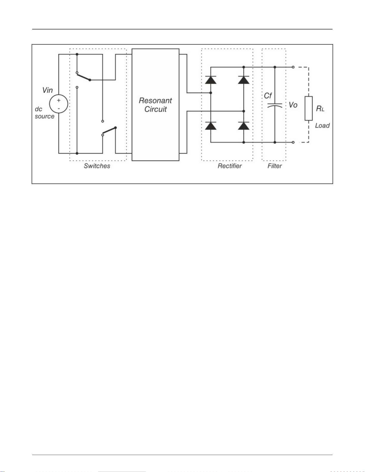
conversion path. Figure 1 shows the typical structure of the resonant converter. The switching network generates a square wave
voltage output. This voltage pattern feeds the resonant tank. The resonant tank consists of a serial or a parallel combination of L
and C passive components. There are several combinations of two or three L and C passive components used in the resonant
tank. The type of resonant tank and its connection to the load defines the resonant converter behaviors. Due to the resonant tank,
the semiconductor switches can operate at zero voltage or current switching condition. This phenomenon significantly reduces
switching losses and allows the converter operation at high switching frequencies.
LLC Resonant Converter Design Using MC56F8xxxx, Rev. 1, 10/2020
Reference Manual 3 / 42
Page 4
NXP Semiconductors
Introduction
Figure 1. Resonant converter principle
The most common known resonant topologies are a Serial Resonant Converter (SRC) and Parallel Resonant Converter (PRC).
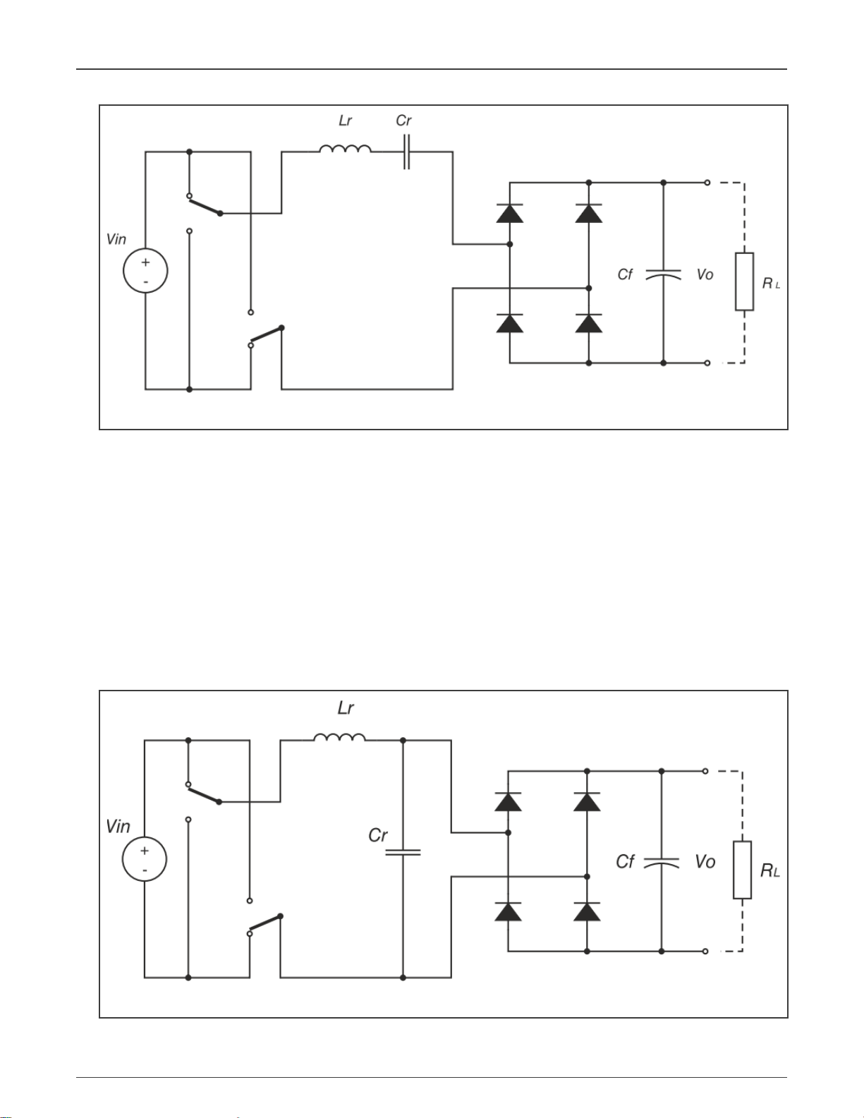
• Figure 2 shows the SRC. The resonant tank consists of a serial connected inductor Lr and capacitor Cr. The load RL is also
connected in series with the resonant tank. In the serial resonant converter, the resonant tank and load creates a voltage
divider. Because the resonant tank impedance is frequency dependent, the output voltage of the SRC can be controlled by
switching frequency. At the DC or low switching frequency the resonant tank has high impedance in comparison with the load
impedance and the output voltage is low. Increasing the switch frequency also increases the output voltage. At the resonant
frequency, the voltage drop on the resonant tank is equal to zero and thus the output voltages are equal to the input voltage.
Continuing over the resonant frequency, the output voltage starts to decrease. This is because the resonant tank impedance
increases against to the load impedance. The operation over the resonant frequency is preferred, even if the output voltage
regulation is possible over or below resonant frequency. The inductive character of the resonant frequency allows to achieve
Zero Voltage Switching (ZVS), which is preferred for MOSFET transistors.
The output voltage regulation is also limited by the load value. If the load is very low, the load impedance is high in comparison
with the resonant tank. Keeping the desired voltage at the output becomes difficult. Theoretically the switching frequency can
be infinite, but practically there is some maximal frequency limit. Therefore, the output voltage regulation at light or no load
condition is very limited.
LLC Resonant Converter Design Using MC56F8xxxx, Rev. 1, 10/2020
Reference Manual 4 / 42
Page 5
NXP Semiconductors
Introduction
Figure 2. SRC topology
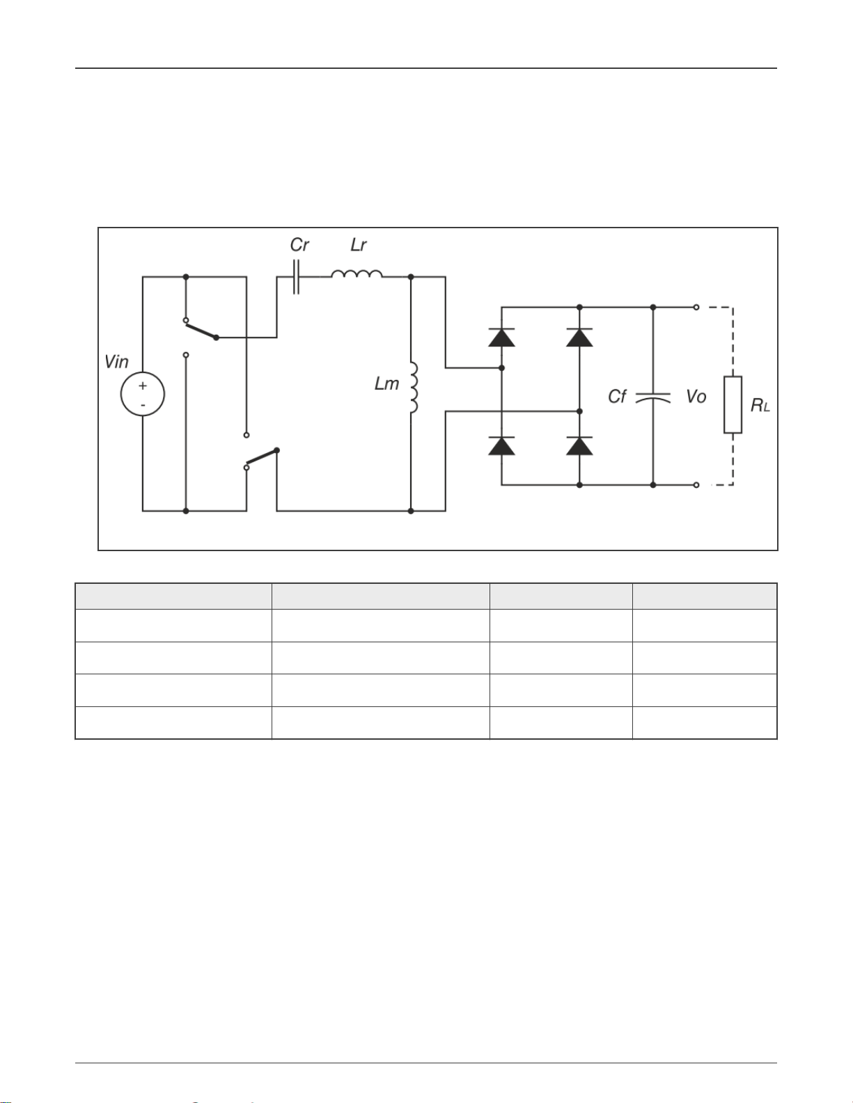
• Figure 3 shows another well-known topology - PRC. The parallel converter uses the same resonant tank as the serial resonant
converter, the serial connection of inductor Lr and capacitor Cr. The PRC differs in load connection to the resonant tank. In this
case, the load is connected in parallel with the capacitor Cr. In this configuration, the voltage divider consists of impedance of
the inductor Lr and impedance of parallel combination of the capacitor Cr and the load RL. This means that both parts top and
bottom impedance of the voltage divider are frequency dependent. At the DC or low switching frequency, the output voltage of
the PRC is equal to input voltages. With the increase of the switching frequency, the output voltage also increases due to the
characteristic of the resonant tank. The maximal output voltage is achieved at a resonant frequency, where the output voltage
is Q times higher than the input voltage. The Q is a quality factor of the resonant tank. Over the resonant frequency, the output
voltage falls, because the inductor impedance becomes more dominant against the capacitor impedance.
The PRC can control the output voltage even at no load conditions. In this case, the PRC is comprised of a resonant tank only.
On the other hand, the permanent connection of the resonant tank to the switch network brings some drawbacks at nominal
operation. At nominal load the parallel converter operates close to the resonant frequency and thus the resonant tanks have
the lowest impedance. This also means a high circulating current through the resonant tank. The parallel converter is also
suggested to operate over the resonant frequency due to ZVS conditions.
Figure 3. PRC topology
LLC Resonant Converter Design Using MC56F8xxxx, Rev. 1, 10/2020
Reference Manual 5 / 42
Page 6
NXP Semiconductors
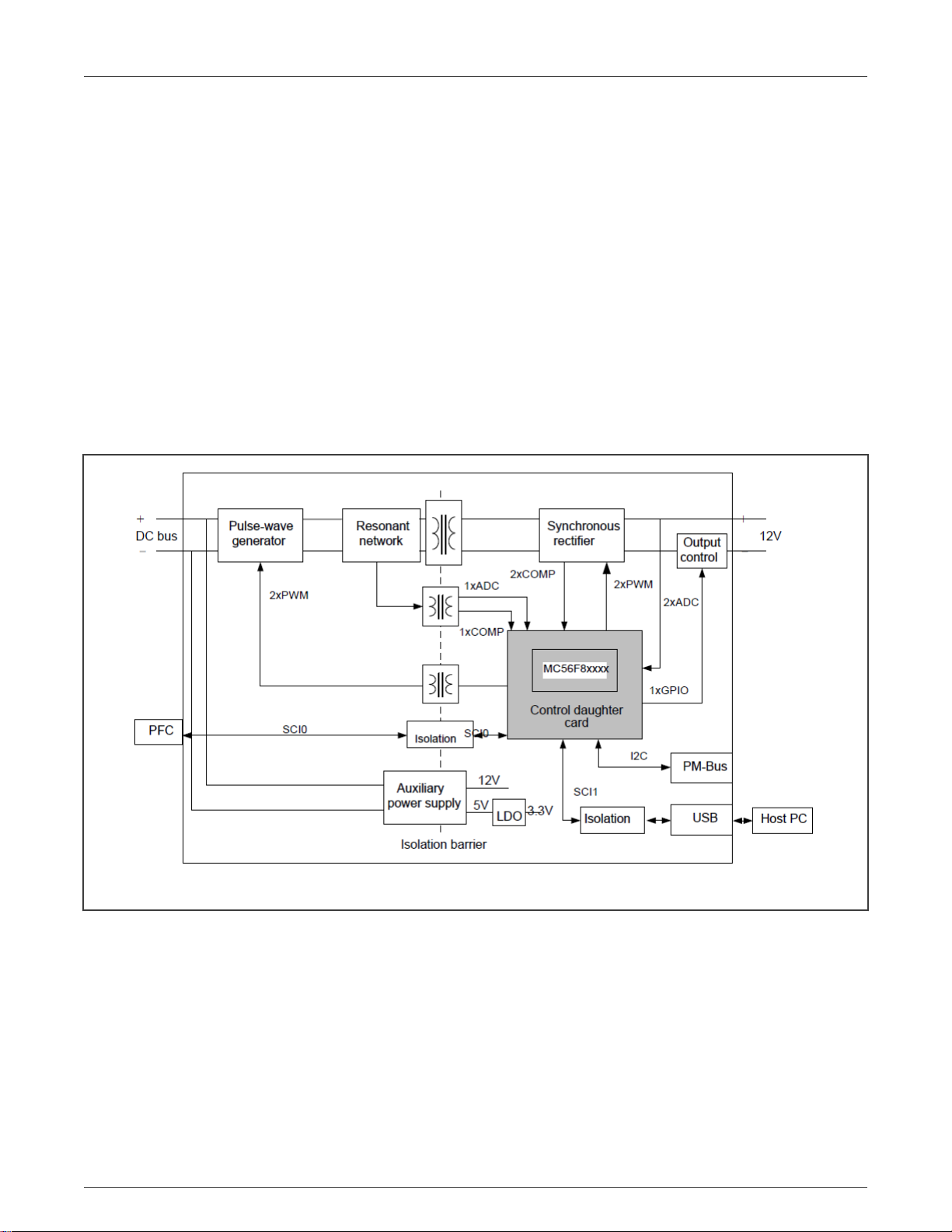
Besides the two part resonant tanks, there are almost 40 possibilities of three part resonant tanks. The most popular member
of three part tanks is the LLC resonant converter. The resonant tank consists of two inductors Lr, Lm and one capacitor Cr (see
Figure 4). The load is connected in parallel to the inductor Lm. The LLC resonant converter solves all drawbacks mentioned
above. At no load conditions the output voltage can still be controlled by a voltage drop over inductor Lm. Also at resonant
frequency, the current is limited by the Lm inductor; therefore, the circulating current through the resonant circuit can be kept
on an acceptable level. Another advantage of the LLC resonant converter is that it can operate under ZVS condition over the
whole load range. Table 1 lists the summary of the key features of all mentioned resonant converters.
Introduction
Figure 4. LLC resonant converter topology
Table 1. Resonant converters comparison
— SRC PRC LLC
ZVS operation Above fr (resonant frequency)only Above fr only Yes
Operation without load No Yes, but high losses Yes
Operation at fr No No Yes
Operation at wide input range High losses High losses Yes
1.3 MC56F8xxxx controller advantages and features
The 56F8xxxx microcontroller is a member of the 32-bit 56800EX core-based Digital Signal Controllers (DSCs). Each device in
the family combines, on a single chip, the processing power of a 32-bit DSP and the functionality of a microcontroller with a flexible
set of peripherals. Due to its cost-effectiveness, configuration flexibility, and compact program code, 56F8xxxx is well-suited for
many consumer and industrial applications.
With numerous, highly-integrated peripherals and powerful processing capabilities, the 56F8xxxx is a low-cost family especially
useful for Switched Mode Power Supplies (SMPSs), advanced motor control (including dual motor control), smart appliances,
Uninterruptible Power Supplies (UPSs), photovoltaic systems, power distribution systems, wireless charging, and medical
monitoring applications.
The following list summarizes the superset of features across the entire 56F8xxxx family.
• 56800EX 32-bit DSC core
• Up to 100MIPS at 100 MHz core frequency
LLC Resonant Converter Design Using MC56F8xxxx, Rev. 1, 10/2020
Reference Manual 6 / 42
Page 7

NXP Semiconductors
Introduction
• Protects supervisor programs and resources from user programs
• One/Two 8-channel eFlexPWM module(s) with NanoEdge™ placement and enhanced capture
• Two 8-channel 12-bit cyclic ADC
• One windowed watchdog timer, power Supervisor;
• On-chip 8 MHz/400 kHz relaxation oscillator, 200 kHz Relaxation Oscillator and 4 MHz to 16 MHz Crystal Oscillator
(XOSC)
• Inter-Module Crossbar with AND-OR-INVERT function
• Programmable Interrupt Controller (INTC)
• One/Two Quad Timer(s), two Periodic Interval Timers
• Two 12-bit DAC modules
• Four High Speed Comparators with integrated DAC references
The switched-mode power supply applications benefit greatly from the flexible eFlexPWM module, fast ADC module, on-chip
analog comparator module, and inter-module crossbar with AOI function.
This PWM module can generate various switching patterns, including highly sophisticated waveforms. It can be used to control
all known motor types and is ideal for controlling different SMPS topologies as well, it has the following features:
• 16 bits of resolution for center, edge aligned, and asymmetrical PWMs;
• Fractional delay for enhanced resolution of the PWM period and edge placement;
• PWM outputs that can operate as complementary pairs or independent channels;
• Support for synchronization to external hardware or other PWM, half cycle reload capability;
• Multiple output trigger events can be generated per PWM cycle via hardware;
• Fault inputs can be assigned to control multiple PWM outputs, programmable filters for fault inputs;
• Independently programmable PWM output polarity, independent top and bottom dead time insertion;
• Each complementary pair can operate with its own PWM frequency and dead time values;
• All outputs can be programmed to change simultaneously via a FORCE_OUT event.
The eFlexPWM offers flexibility in its configuration, enabling efficient control of any SMPS topology. The eFlexPWM module is
capable of free control of rising and falling edges for each PWM output and includes automatic complementary signal generation
and dead time insertion. Due to NanoEdge placement the eFlexPWM can generate duty cycles and frequencies with high a
resolution of up to 312 ps. The eFlexPWM module can also generate up to six synchronization events per sub-module to provide
synchronization with other modules (ADC, Quad-timer).
This LLC resonant converter application uses the eFlexPWM module for generating two PWM signals for primary side power
MOSFETs and two PWM signals for secondary side synchronous rectifier, and provide the trigger signal for ADC sample.
The Analog-to-Digital Converter (ADC) function consists of two 12-bit resolution separate ADC, each with eight analog inputs and
its own sample and hold circuit. A common digital control module configures and controls the functioning of the converters. ADC
features include:
• Two independent 12-bit ADCs:
— Two 8-channel external inputs
— Built-in × 1, × 2, × 4 programmable gain pre-amplifier
• Support of analog inputs for single-ended and differential, including unipolar differential, conversions.
• Sequential, parallel, and independent scan mode.
• First eight samples have offset, limit and zero-crossing calculation supported.
LLC Resonant Converter Design Using MC56F8xxxx, Rev. 1, 10/2020
Reference Manual 7 / 42
Page 8

NXP Semiconductors
Introduction
• ADC conversions can be synchronized by any module connected to the internal crossbar module, such as PWM, timer,
GPIO, and comparator modules.
• Support for simultaneous triggering and software-triggering conversions.
• Support for a multi-triggering mode with a programmable number of conversions on each trigger.
• Each ADC has ability to scan and store up to eight conversion results.
This LLC resonant converter application uses the ADC module in triggered parallel mode, it is synchronized at the center of PWM
signal. ADCA sampled the output current and primary current, ADCB sampled output voltage and input voltage.
The Inter-Module Crossbar and AND-OR-INVERT logic features:
• Provides generalized connections between and among on-chip peripherals: ADCs, 12-bit DAC, comparators, quad-timers,
eFlexPWMs, EWM, and select I/O pins.
• User-defined input/output pins for all modules connected to the crossbar.
• DMA request and interrupt generation from the crossbar.
• Write-once protection for all registers.
• AND-OR-INVERT function provides a universal Boolean function generator that uses a four- term sum-of-products
expression, with each product term containing true or complement values of the four selected inputs (A, B, C, D).
This LLC resonant converter application uses the Inter-Module Crossbar and AND-OR-INVERT logic to provide interconnection
between the eFlexPWM module and ADC module, interconnection between fault signal and on-chip comparator, generate the
synchronization rectifier PWM by multiple signals from eFlexPWM and on-chip comparator.
The application also uses other peripherals like on-chip comparator for hardware protection and secondary side voltage
zero-cross detection, a PIT module for the software timer, 2xSCI module for communication with the primary side and remote
control via PC and several GPIOs for LED indication.
LLC Resonant Converter Design Using MC56F8xxxx, Rev. 1, 10/2020
Reference Manual 8 / 42
Page 9
NXP Semiconductors
Chapter 2
System description
2.1 Structure
LLC is an isolated buck-boost converter, and the isolation between the primary and secondary side is formed by transformer.
The primary side incorporates the pulse-wave voltage generator, resonant network, isolated drivers, and isolated UART port to
communicate with other devices, such as, the front stage PFC converter.
The secondary side incorporates the synchronous rectifier, voltage/current sensing circuitry, output controller, drivers, PM Bus
communication, and the DSC controller board.
The auxiliary power supply takes the power directly from the DC Bus, and then generates the desired voltages with the
Flyback converter.
Figure 5 shows the overall system structure.
Figure 5. System block diagram
The sensing circuitries are used for sensing DC Bus voltage, resonant current, output voltage, output current and accommodating
them to the MCU acceptable voltage level.
The drivers are used for amplification of MCU PWM signals. Isolated drivers are between the primary and secondary side for the
driving of the resonant converter’s MOSFET on the primary side, which is implemented by pulse transformer. Non-isolated drivers
are used for synchronous rectifier’s MOSFET on the secondary side.
The synchronous rectifier rectifies the output voltage to 12 V level and can reduce the conduction losses. The output controller
determines the load on or off by software.
The DSC MC56F8xxxx controller is situated on the control daughter card and connected to the power board via the PCI slot. The
control card is powered from the secondary side and it works as the master for the whole application.
LLC Resonant Converter Design Using MC56F8xxxx, Rev. 1, 10/2020
Reference Manual 9 / 42
Page 10
NXP Semiconductors
System description
The controller is also used to communicate with outside devices. One isolated UART is applied to communicating with the
front PFC stage. Another UART to USB conversion is applied to communicating with the host PC for FreeMASTER or firmware
updating. One IIC is reserved for the PM Bus network.
2.2 Modulation mode
Most conventional LLC resonant converter applies the Pulse Frequency Modulation (PFM), namely complementary pulse signals
with 50% duty cycle drive the upper and lower arm switch and regulate the output voltage by adjusting the switching frequency.
Assuming that the power is transferred mainly by the fundamental component, the First Harmonic Approximation (FHA) method
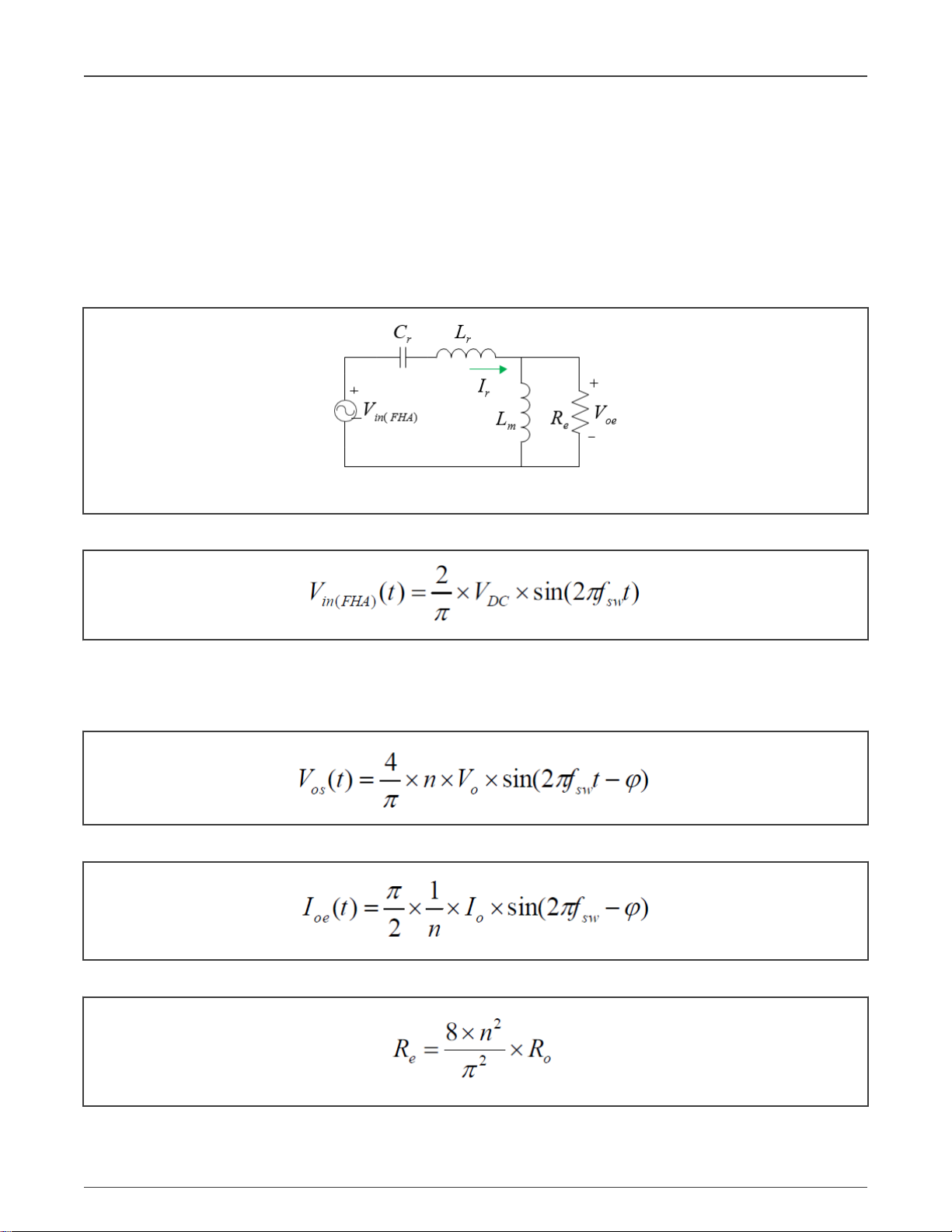
can be used to analyze the LLC resonant converter. Figure 6 shows the equivalent circuit of LLC resonant converter.
Figure 6. Equivalent circuit of LLC resonant converter
V
is the fundamental component of the output of pulse-wave generator.
in(FHA)
Voe is the fundamental component of the output voltage in the primary side, where:
• φ is the phase angle between Voe and V
in(FHA)
• n is the transformer turn ratio
Fundamental component of current Ioe.
Re is the AC equivalent load on the primary side.
Then, the input-to-output voltage gain can be obtained.
LLC Resonant Converter Design Using MC56F8xxxx, Rev. 1, 10/2020
Reference Manual 10 / 42
Page 11
NXP Semiconductors
Where:
•
•
•
•
System description
• fsw is the operating frequency
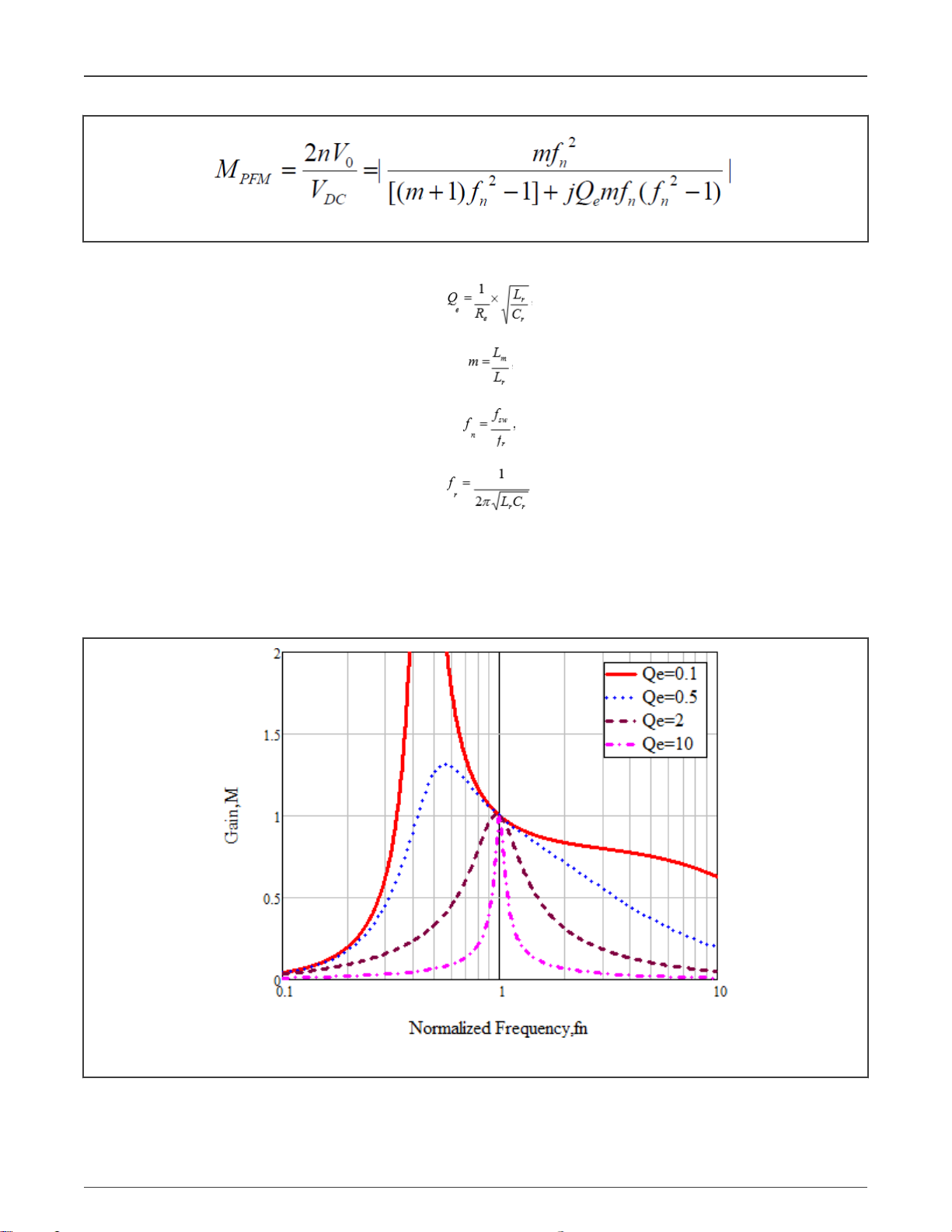
For a more intuitive understanding of the modulation principles, it is necessary to know how voltage gain behaves as a function
of fn, m, and Qe. The value of m is fixed after the physical parameters are determined and the quality factor Qe is now only
load-dependent which is also fixed in certain condition. Therefore, it is wise to plot M with respect to fn for different values of Qe.
As seen in Figure 7, the value of M varies with fn under certain m and Qe.
Figure 7. Plots of PFM voltage gain function
However, it is also obvious that the variation range of M is limited when fn > 1. To meet the requirements of a wide input voltage,
improving the switching frequency unlimitedly is not desirable, because of the restriction of component availability, the effect of
the transformer parasitic parameters, and so on.
LLC Resonant Converter Design Using MC56F8xxxx, Rev. 1, 10/2020
Reference Manual 11 / 42
Page 12
NXP Semiconductors
System description
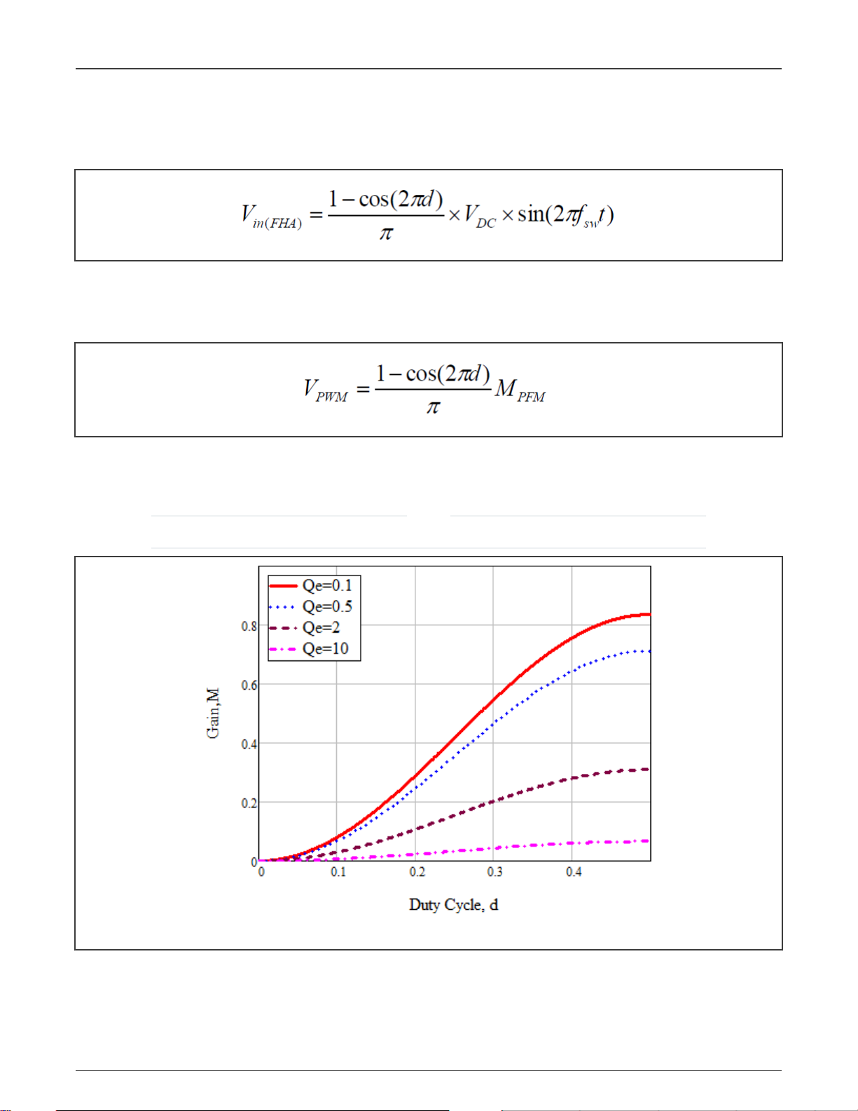
Considering the above contradictions, the additional symmetric Pulse Width Modulation (PWM) mode, namely adjusting duty
cycle of fixed frequency drive signals to regulate the output voltage, is desired.
When using symmetric PWM, V
expresses as:
in(FHA)
Where:
• d represents the duty cycle of the drive signal.
Then the voltage gain can be obtained.
Assuming a fixed working frequency which is larger than the resonant frequency, Figure 8 shows the voltage gain function for
different values of Qeunder PWM mode. The voltage gain can be any value between 0 and 1 when the duty cycle varies from 0
to 0.5.
NOTE
In order to ensure ZVS, the duty cycle can’t be too small. This reference chooses 0.3 as the minimum duty cycle.
Figure 8. Plots of PFM voltage gain function
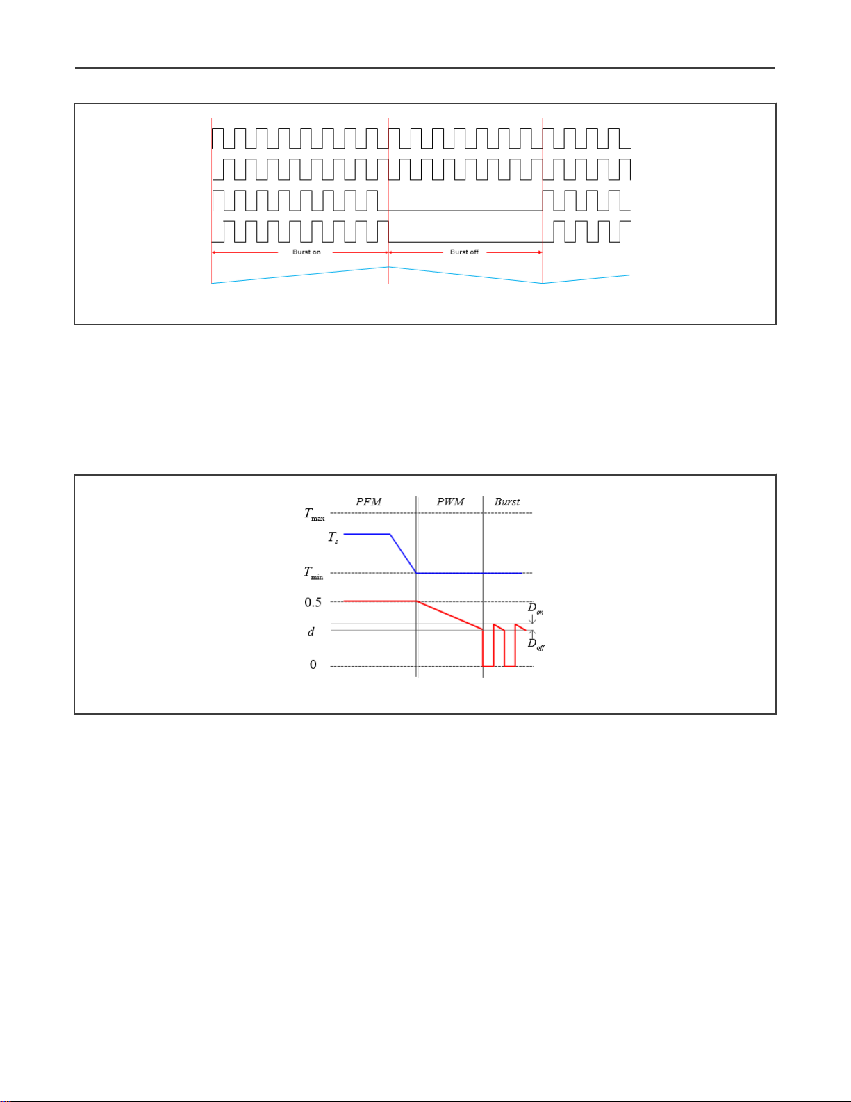
When the input voltage is too high or the load is too light, the symmetric PWM mode may still not meet requirements. So the
burst mode, namely blocking switching drive signals periodically, is taken. The burst mode control can also improve the light load
efficiency of the LLC converter. Figure 9 shows the burst operation processes. When the drive signals are not blocked, the output
voltage rises, and conversely declines.
LLC Resonant Converter Design Using MC56F8xxxx, Rev. 1, 10/2020
Reference Manual 12 / 42
Page 13
NXP Semiconductors
System description
Figure 9. Waveforms of Burst operation
As seen in Figure 7, the voltage gain decreases as the switching frequency increases in the inductive area, while in Figure 8,
the voltage gain decreases as the duty cycle decreases. In PFM mode, when the maximum switching frequency can’t meet the
gain requirement, transfer to PWM mode. If the minimum duty cycle still can’t meet requirements, transfer to burst mode. In the
closed-loop control, we take the required duty cycle which reflect the current state of the system instead of output voltage as the
judgement condition to smoothly switch between different modes. Figure 10 shows the condition of each mode and the transition
between them, a hysteresis is taken in burst mode to avoid frequent switching. In Figure 10, T
switching period, T
is the allowed minimum period, D
min
is minimum allowed duty cycle, Don and D
off
is the allowed maximum
max
is the upper and lower
off
limitation of hysteresis.
Figure 10. PFM, PWM and burst modes
2.3 Control loop introduction
In the server, the battery charger and many other industrial applications, the power supplies are required to have both constant
voltage and overload current limiting control. So the dual outer loop control scheme is applied, it includes the inner primary current
loop and outer output voltage or out current loop determined by the output current. The inner average current control loop is applied
to eliminate the difference in small-signal characteristics among different static operation, which is equivalent to modify the object
model, to adapt to the wide range requirement. Figure 11 shows the control scheme.
LLC Resonant Converter Design Using MC56F8xxxx, Rev. 1, 10/2020
Reference Manual 13 / 42
Page 14

NXP Semiconductors
System description
Figure 11. LLC control scheme
With this control scheme, LLC can work under three states:
• S1 constant voltage state: System mainly working under this mode to maintain constant 12V output. Output voltage
equals its reference and output current smaller than its reference, negative deviation causes the PI result of output current
regulator reaches its upper limit which is zero. So the output current loop is calculated but has no effect on the control, the
control signal is only related to output voltage.
• S2 constant current state: When output current reaches the current limitation threshold, output voltage decrease and
constant current loop takes effect. Output current equals its reference and output voltage smaller than its reference,
continuing positive deviation causes the PI result of the output voltage regulator has been equals its upper limit. So even if
the voltage loop is calculated, only the change of output current takes effect.
• S3 transient state: It is the intermediate state when switching between S1 and S2 and both the voltage and current loop
take effect in this state. If the load exceeds the rated load in constant voltage mode, system will change from constant
voltage state to constant current state. In this process, the PI result of voltage loop increases and the PI result of current
loop decreases. If the load reduces to less than ratings, system changes from constant current loop to constant voltage
loop. In this process, the PI result of voltage loop decreases and the PI result of current loop increases.
In summary, the concurrent outer loop smooth transition achieves both constant output voltage and overload current limitation.
The resonant current inner loop ensures the good performance in all range with the same controller. Figure 12 shows the output
I-V curve.
Figure 12. Dual outer loop I-V curve
LLC Resonant Converter Design Using MC56F8xxxx, Rev. 1, 10/2020
Reference Manual 14 / 42
Page 15

NXP Semiconductors
Chapter 3
Hardware design
This chapter describes the LLC resonant converter hardware design, provides the design procedure of resonant network and
transformer, provide the layout consideration for high frequency, high voltage, large current LLC resonant converter use case.
3.1 Specifications
Table 2. LLC resonant converter specifications
Maximum input voltage V
Minimum input voltage V
Nominal input voltage V
Output voltage V
Output current I
Secondary-side voltage drop V
Current limitation threshold I
Efficiency η 92%
Maximum switching efficiency f
Minimum switching efficiency f
Resonant frequency f
Lm/Lr ratio m 4
in_ max
in_ min
in_nom
o
o
F
lim
max
min
r
400 V
330 V
380 V
12 V
20 A
0.3 V
22 A
250 kHz
70 kHz
110 kHz
3.2 Resonant network design
Determine the maximum and minimum voltage gains of the resonant network. m is the ratio between Lm and Lr. A higher peak
gain can be obtained with a small m value, but too small m value results in poor coupling of the transformer and deteriorates the
efficiency, usually m can be chosen between 3 and 7. In the reference design, m is selected as 4.
The transformer turns ratio can be determine according to the nominal input voltage,
The required gain at maximum and minimum input voltage can be determined with the following equations.
LLC Resonant Converter Design Using MC56F8xxxx, Rev. 1, 10/2020
Reference Manual 15 / 42
Page 16

NXP Semiconductors
Hardware design
Qe can be determined according to gain curves (as shown in Figure 7). In the reference design, taking 10% gain margin and
operating frequency range into considerations, then Qe is selected as 0.36.
Calculate the equivalent load resistance:
The resonant circuit consists of resonant capacitor Cr and resonant inductor Lr. The resonant parameters can be calculated as:
The magnetizing inductance can be calculated as:
In the reference design, Cr is selected as 40 nF, and Lr is selected as 52 uH.
3.3 Transformer design
In an actual transformer, the resonant inductor can be integrated into the transformer, the primary inductance equals to:
And for integrated transformer, the actual turn ratio of transformer should be calculated according to the following equation.
LLC Resonant Converter Design Using MC56F8xxxx, Rev. 1, 10/2020
Reference Manual 16 / 42
Page 17

NXP Semiconductors
Hardware design
The transformer core can be determined according to the output power, and after the core is selected, the Aeis also determined.
The secondary and primary turns can be calculated according to the following equations.
In the reference design, integrated transformer is used. Considering the power, ETD44 coil is selected, the flux density swing is
selected as 0.3 T to reduce losses in the magnetic core,Np is selected as 32 turns and Ns is selected as 2 turns.
3.4 Power circuits and drivers
Figure 13 shows the power circuits for both the primary side and secondary side, including the primary side power MOSFETs,
resonant capacitor, main transformer, synchronize rectifier, output filter, and analog sensor circuits.
Figure 13. Main power circuit
Figure 14 (a) shows the primary side MOSFET drive circuits. The resistors and capacitors were select to provide smooth drive
signal and avoid the transistor to enter deep saturation. Figure 14 (b) shows the secondary side SR MOSFETs drive circuits.
LLC Resonant Converter Design Using MC56F8xxxx, Rev. 1, 10/2020
Reference Manual 17 / 42
Page 18

NXP Semiconductors
Hardware design
Figure 14. PWM drive circuits
Figure 15 shows the zero crossing signal detection signal for synchronize MOSFETs, sec_2 connect to secondary coil of main
transmitter, I_SR2 connect to the internal comparator DSC to provide the zero crossing signal for SR divers.
LLC Resonant Converter Design Using MC56F8xxxx, Rev. 1, 10/2020
Reference Manual 18 / 42
Page 19

NXP Semiconductors
Figure 15. Zero-crossing signal detection circuits
Hardware design
Figure 16 shows the primay current detection circuits. One 1:50 current sensor is used and one channel connect to DSC
comparator for hardware protection, another channle connect to ADC for inner primary current loop control, adjust the resistor and
capacitor value can change the signal frequency bandwindth.
Figure 16. Primary current detection circuits
3.5 PCB layout considerations
In LLC resonant converter reference design, input voltage is high, input current is large, output current is larger than 20 A,
and the system is working in high-frequency mode (70-250 K). Thus the PCB layout need to be well considered, especially for
following points:
• The input and output current loop routing;
• Power ground copper pouring to avoid influence by high frequency signal;
• Heat dissipation for power components;
• The absorb circuits should be put on top layer and close to relative pin;
LLC Resonant Converter Design Using MC56F8xxxx, Rev. 1, 10/2020
Reference Manual 19 / 42
Page 20

NXP Semiconductors
Hardware design
• Safety distance consideration for primary side and secondary side;
• Differential routing for current sample lines.
Figure 17 and Figure 18 show the input and output current routing, use power lines as thick as possible, the power loop as small as
possible. Make sure the output current flow through the filter circuits first before it arrived at the output port. Pour cropper around
the power components and add tin window on the surface for heat dissipation.
Figure 17. Primary side current loop
LLC Resonant Converter Design Using MC56F8xxxx, Rev. 1, 10/2020
Reference Manual 20 / 42
Page 21

NXP Semiconductors
Hardware design
Figure 18. Secondary side current loop
Figure 19 shows the safe distance between primary side and secondary side, which is larger than 6 mm for reinforce insulation.
The primary side to ground insulation is larger than 2.5 mm for high input voltage, and the secondary side to ground insulation is
larger than 1 mm.
LLC Resonant Converter Design Using MC56F8xxxx, Rev. 1, 10/2020
Reference Manual 21 / 42
Page 22

NXP Semiconductors
Hardware design
Figure 19. Safety distance between primary and secondary side
Additionally, the ground is not poured as large as possible, especially not poured below the high frequency circuits, only meets
the current level and heat dissipation, thus to avoid the import of high frequency system operation interfere.
LLC Resonant Converter Design Using MC56F8xxxx, Rev. 1, 10/2020
Reference Manual 22 / 42
Page 23

NXP Semiconductors
Chapter 4
Software design
This application core is the MC56F8xxxx DSC. This low-cost DSC has enough peripherals and features suitable for
implementation of full digital control of LLC resonant converter.
The software is written in C language using Code Warrior, and calls the embedded software library (FSLESL) for time saving.
For more information about how to use these libraries in the Code Warrior project, see
Software Libraries in Code Warrior
This section describes the design of the software blocks, including software structure, configuration of the DSC peripherals, control
timing, implementation of codes run in ram, and boot loader.
(document AN4586).
4.1 Parameter normalization
In order to make full use of DSC resources, the application related physical quantities are all normalized to fixed-point decimal
format, namely Q data format.
The relationship between actual value of the physical quantity and its normalized value is shown as following:
Where:
Inclusion of DSC Freescale Embedded
Where:
• Frac value is the normalized value of the physical quantity.
• actual value is the actual value of the physical quantity expressed in unit.
• quantization range is the maximum measurable value of this physical quantity.
4.2 State machine
Figure 20 shows how this application uses the state machine to control the system flow. After resetting the DSC to configure
all peripherals, the system enters a never-ending loop, including the application state machine. The application state machine
includes four states:
• INIT: The variable initialization.
• STOP: The system is initialized and waiting for the Run command, and the PWM output is disabled.
• RUN: The system is running, the run sub-state is called, and the PWM output is enabled and can be stopped with the Stop
command.
• FAULT: The system faced a fault condition and the PWM output is disabled.
After the parameters initialization, the application state machine continues into the STOP state. In the STOP state, different control
algorithms can be configured by FreeMASTER online:
• Open loop;
• Voltage single loop: the Constant output voltage control with a single loop;
• Voltage/current dual loops: the output voltage control with the voltage outer loop and the primary current inner loop;
• CCM/CVM outer loops: the concurrent output voltage or the current control with the primary current inner loop.
LLC Resonant Converter Design Using MC56F8xxxx, Rev. 1, 10/2020
Reference Manual 23 / 42
Page 24

NXP Semiconductors
Software design
Besides, the software regularly checks the LLC_run instruction to decide whether to start up. When the command, LLC_run,
is set, the application state machine continues into the RUN state. In this state, the controller starts to take effect to achieve
constant output voltage or limiting output current. Besides, the LLC_run instruction is also regularly checked in RUN state. When
the command, LLC_run, is cleared, the application state machine goes back to STOP state and waits for the LLC_run command
to be set again.
The fault detection executes under all states. If any fault is detected, the application state machine enters the FAULT state. In
this state, fault detection is still executed and whether to restart the application is optional. If allowed, when the fault condition is
certainly cleared, the application state machine restarts from the INIT state. If not, the software stays in a never ending loop and
output of the converter is disabled. The system needs to power up again for a restart.
Figure 20. Application main state machine
The RUN state is divided into two sub-state according to LLC application, as shown in Figure 21. When application state
machine transits from STOP to RUN, the system first comes into the soft-start sub-state and starts LLC resonant converter to
run with maximal switching frequency and changeable duty cycle which is determined by current output voltage. The duty cycle
is increased following the ramp until it reaches 50%. After that, the switching frequency is decreased following the ramp until a
certain output level is reached. Then the sub-state continues into the normal state and the closed-loop controller works to calculate
the desired duty cycle and switching frequency. In this sub-state, the reference output voltage is increased following ramp until it
reaches desired value and the load is connected when output voltage reaches its final reference.
LLC Resonant Converter Design Using MC56F8xxxx, Rev. 1, 10/2020
Reference Manual 24 / 42
Page 25

NXP Semiconductors
Figure 21. Application run sub-state
The application main state machine is declared in state_machine.c and state_machine.h. It is declared as:
Software design
/* State machine control structure */
typedef struct
{
pmem SM_APP_STATE_FCN_T const* psState; /* State functions */
pmem SM_APP_TRANS_FCN_T const* psTrans; /* Transition functions */ SM_APP_CTRL uiCtrl; /* Control
flags */
SM_APP_STATE_T eState; /* State */
} SM_APP_CTRL_T;
It consists of four parts:
• psState is the user end state function.
• psTrans is the user end transition function. When the system transfers between different states, corresponding transition
function is called.
• uiCtrl is the system flow control flag.
• eState is the current state of the state machine.
The state machine is periodically called in the software by inline function which calls the user defined state function. The
corresponding user end state functions and transition functions are defined in LLC_statemachine.c.
/* pointer to function with a pointer to state machine control structure */
typedef void (*PFCN_VOID_PSM)(SM_APP_CTRL_T *sAppCtrl);
/* State machine functions field (in pmem) */
pmem const PFCN_VOID_PSM gSM_STATE_TABLE[4] = {SM_StateFault, SM_StateInit, SM_StateStop,
SM_StateRun};
/* State machine function */
extern inline void SM_StateMachine(SM_APP_CTRL_T *sAppCtrl)
{
gSM_STATE_TABLE[sAppCtrl -> eState](sAppCtrl);
}
LLC Resonant Converter Design Using MC56F8xxxx, Rev. 1, 10/2020
Reference Manual 25 / 42
Page 26

NXP Semiconductors
Software design
The sub-state functions and corresponding transition functions are defined in LLC_statemachine.c and are called when the
system is in the RUN state as the same way as the main state.
4.3 Control timing
The LLC software consists of two periodical interrupts and a background loop. The first periodical interrupt PWM_Trigger_ISR()
is driven by the VAL0 compare event from eFlexPWM SM0. This routine is configured for higher priority to execute the control
loop calculation and get the desired switching signal. The ADC conversion is triggered at the same time, so register push and
ADC sampling operate simultaneously which leaves more time for algorithm calculation. Besides, center aligned PWMs ensure
this sampling point not affected by the switching operation and can get precise sample result.
PIT0_ISR() is called every 1 ms by the roll-over event of PIT0. This routine is used to create a 1 ms time base which can be used as
software timer for protection and so on. The background loop runs in a never ending loop. It includes the application state machine
and communication with PC (FreeMASTER).
As can be seen from the above description, PWM_Trigger_ISR() is a time critical routine. The FSLESL is applied to minimize
the total execution time. However, because of the high switching frequency, this routine still can’t execute every switching period
under each switching frequency. In order to achieve more precise control, the application tries to increase the effective controlling
frequency by two ways:
• Run the time critical algorithm in RAM which is described in detail in the following section.
• Change the controlling frequency according to current switching frequency.
So we need different eFlexPWM sub-modules to handle controlling frequency and PWM generating. MC56F8xxxx eFlexPWM
module has four sub-modules SM-4. SM0 is used to determine the controlling frequency and synchronize the ADC sample.
SM1&2 are used to construct PWM signals need by switch drivers. The synchronization between different sub-modules is
achieved by master reload signal forcing initialization. As measurement, the maximum time from PWM event trigger to the end
of interrupt is 8.2 µs, which includes the outer output current limitation loop, output voltage loop and inner primary voltage loop.
So the application takes 10 µs as the minimum control period, which means when the switching frequency is lower than 100 kHz
the controller is executed every PWM period. So the modulo count value of SM0 and SM2 are equivalent. When the switching
frequency is between 100 kHz and 200 kHz, the controller is executed every two PWM periods. So the modulo count value of SM0
is two times of SM2. When the switching frequency is between 200 kHz and 300 kHz, the controller is executed every three PWM
periods. So the modulo count value of SM0 is three times of SM2.
As mentioned in State machine, LLC RUN state is divided into two sub-states. Figure 22 shows the control timing for soft-start
state. The start-up frequency fst is set to 250 kHz which lets the controller execute every three PWM periods. Figure 23 shows the
control timing for normal state. When switching frequency is lower than 200 kHz, duty cycle is fixed at 50%. LLC converter works
under PFM mode. When the desired frequency is higher than 200 kHz, switching frequency is fixed at 200 kHz and LLC converter
works under symmetric PWM mode.
LLC Resonant Converter Design Using MC56F8xxxx, Rev. 1, 10/2020
Reference Manual 26 / 42
Page 27

NXP Semiconductors
Software design
Figure 22. Control timing for soft-start state
Figure 23. Control timing for normal state
The controlling frequency change is implemented in LLC_PWM_UPDATE() function as:
if(f16Ts <= (LLC_Drive.sPerCtrl.f16Ts_Lim1))
{
LLC Resonant Converter Design Using MC56F8xxxx, Rev. 1, 10/2020
Reference Manual 27 / 42
Page 28

NXP Semiconductors
Software design
setReg16(PWMA_SM0VAL1,(Ts*6)-1 );
}
else if(f16Ts <= LLC_Drive.sPerCtrl.f16Ts_Lim2)
{
setReg16(PWMA_SM0VAL1, (Ts<<2)-1);
}
else
{
setReg16(PWMA_SM0VAL1, (Ts<<1)-1);
}
4.4 Drive signal generation logic
Drive signals for half bridge MOSFETs are generated by eFlexPWM SM2. The generated PWMs can output directly or connect
to internal-peripheral crossbar switch (XBAR). When it is connected to XBAR, the hardware fault signal can connect to XBAR too
and AND with the PWMs through AOI to generate the final drive signal.
Precise synchronous rectification drive signals combine the hardware detection signal and eFlexPWM SM1 PWMs through AOI
AND function. Detected hardware signal is the DS voltage of sync tube and SM1 PWMs is a little delay to half bridge MOSFET
PWMs. The combination and delay ensure the correctness and accuracy of synchronous rectification drive signals which minimize
the loss of diode rectification. Fault signal is also needed to close the synchronous rectification MOSFETs.
Figure 24 shows the drive signal generation logic. The SW PWM output control is used to on/off the PWM outputs flexibly.
PWM_1&2 are the half bridge MOSFET drive signals and PWM_SR1&2 are the synchronous rectification drive signals. All
combinations are implemented by hardware which ensures the timeliness of drive signal and simplifies the software design.
Figure 24. Drive signal generation logic
LLC Resonant Converter Design Using MC56F8xxxx, Rev. 1, 10/2020
Reference Manual 28 / 42
Page 29

NXP Semiconductors
Software design
4.5 Fault protection
The hardware protection is over-current protection of resonant current, which is generated by the build- in high speed comparator
A. And the fault threshold is set to 4.2 A.
The software protection includes resonant current over-current protection, output under-voltage and over-voltage protection,
output over-current protection. Under the CCM/CVM outer loops mode, the output current is limited so the output under-voltage
will take effect if the load is too heavy. Under other conditions, the output current protection takes effect and the overload duration
is considered. 50% overload duration is now set to 5 ms and 20% overload duration is 20ms, which can be easily modified
as needed.
4.6 Use of peripherals
4.6.1 ADC converter
The ADC A&B converters are set to run simultaneously and synchronize with eFlexPWM sub-module 0 via Trigger 0. The trigger
signals connection between eFlexPWM and ADC is provided by a cross bar switch module. The ADC A samples resonant current
and output current, ADC B samples DC bus voltage and output voltage.
4.6.2 Pulse width modulator eFlexPWN
• The eFlexPWM sub-module 0 is used for timing control and no PWM signal is generated from this sub-module. Register
VAL0 is used to generate trigger signal for ADC and cause interrupt to handle control algorithm. Modulo count value VAL1
varies according to current switching frequency.
• The eFlexPWM sub-module 2 generates two complementary PWM signals. The PWM outputs have variable frequency
and duty cycle and route to XBARB for the generation of half bridge MOSFET drive signals. The variation of duty cycle
is implemented by change of dead time generated by software. Due to NanoEdge placement this module can generate
duty cycle and frequencies with higher resolution up to 520 ps. The sub-module 2 is synchronized with sub- module 0 by
master reload forcing initialization.
• The eFlexPWM sub-module 1 has the same modulo count value with sub-module 2 and generates two complementary
signals. The PWM outputs have the variable frequency as sub- module2 and route to XBARB for the generation of
synchronous rectification MOSFET drive signals. During operation above resonant frequency the synchronous rectification
MOSFETs can switch off later than half bridge MOSFET. This means the falling edge comes later in comparison with the
primary PWM signals.
Therefore, the PWM outputs of sub-module 1 are same as sub-module 2 except the falling edge. During operation below resonant
frequency the earlier shutdown is achieved by hardware detection. The sub- module 1 is also synchronized with sub-module 0 by
master reload forcing initialization, so it is synchronized with sub-module 2.
4.6.3 High speed comparator HSCMPA
The build-in high speed comparator A is used to detect over current condition of the primary resonant current. One of the
comparator’s inputs is the measured resonant current, the other is the fault threshold set by VREF A.
4.6.4 High speed comparator HSCMPB&D
The build-in high speed comparator B&D are used to detect the voltage flip of transformer for synchronous rectification MOSFET
on/off control. The transformer voltage thresholds are set by VREF B&D.
4.6.5 Inter-peripheral crossbar switch XBARA&B and AOI
Crossbar switch A provides the connection for trigger signals between eFlexPWM and ADC. It also works together with crossbar
switch B and AOI module to generate the precise drive signals. PWM outputs of submodule 1&2, comparator A&B&D outputs are
transferred to AOI module through XBAR B. The logical operation results of AOI are exported through XBAR A.
LLC Resonant Converter Design Using MC56F8xxxx, Rev. 1, 10/2020
Reference Manual 29 / 42
Page 30

NXP Semiconductors
Software design
4.6.6 Periodic interrupt timer PIT0
The periodic interrupt timer 0 is configured to generate a periodical interrupt every 1ms, which create a time base for use.
4.6.7 Serial communication interface SCI0 & SCI1
The serial communication interface SCI0 is used for communication with front stage, it can exchange the information with PFC
side, accept the control instructions and execute.
The serial communication interface SCI1 is used for communication with the host PC for FreeMASTER or firmware updating.
There is also a SCI USB converter on the board, so the communication with host PC finally goes via USB interface.
4.6.8 GPIO pins
There are two GPIO outputs used to drive the fault LEDs. The green LED (D4) is connected to GPIO F6 which is lit when hardware
protection occurs. The red LED (D3) is connected to GPIO C0 which is lit when software protection occurs. Other GPIO pins used
by peripherals are set to the peripheral mode.
4.7 Code runs in RAM
Due to the limitation of code execution speed in Flash, the time critical routine PWM_Trigger_ISR() is configured to runs in RAM
for time saving.
Because RAM is volatile, the relocated code is stored in flash and copied into RAM during microcontroller start-up. In order to
realize this goal, take the following steps:
1. Disable the auto generated LCF by processor Export option if used, as shown in Figure 25.
Figure 25. Disabling LCF auto generation
2. Define code sections with pragma directive. Both the PWM_Trigger_ISR() routine and the functions called in it are included
in this section.
#pragma define_section ramCodes_main "ramFunc_main.text" RX
#pragma section ramCodes_main begin
#pragma interrupt saveall
void PWM_Trigger_ISR(void)
{ … }
#pragma interrupt off
#pragma section ramCodes_main end
pragma define_section ramCodes_llc "ramFunc_llc.text" RX
#pragma section ramCodes_llc begin
static void LLC_StateRun_Softstart(void) #pragma section ramCodes_llc end
#pragma section ramCodes_llc begin
LLC Resonant Converter Design Using MC56F8xxxx, Rev. 1, 10/2020
Reference Manual 30 / 42
Page 31

NXP Semiconductors
Software design
static void LLC_StateRun_Normal(void)
{ … }
#pragma section ramCodes_llc end
#pragma section ramCodes_llc begin
static void LLC_TransRun_Softstart_Normal(void)
{ … }
#pragma section ramCodes_llc end
3. Shrunken the .p_Code memory segment length and assign a size fixed flash area for relocated code with Linker Command
File (LCF). Different device has different memory map, take MC56F82748 for example.
MEMORY {
.x_Peripherals (RW) : ORIGIN = 0xC000, LENGTH = 0
# List of all sections specified in the "Build options" tab
.p_Interrupts (RWX) : ORIGIN = 0x00000000, LENGTH = 0x000000DE
.p_Code (RWX) : ORIGIN = 0x00000208, LENGTH = 0x00002DF5
.x_Data (RW) : ORIGIN = 0x00000000, LENGTH = 0x00001000
.p_reserved_FCF (RWX) : ORIGIN = 0x00000200, LENGTH = 0x00000008
.x_internal_ROM (RW) : ORIGIN = 0x000040DE, LENGTH = 0x00000122
.p_ramFuncCode (RWX) : ORIGIN = 0x00002FFD, LENGTH = 0x00001000
.p_ramFuncSpace (RWX) : ORIGIN = 0x0000F000, LENGTH = 0x00001000
.p_flash_ROM_data (RX) : ORIGIN = 0x00000000, LENGTH = 0x00001000
}
4. Reside the defined code section in corresponding section segment with LCF. And remember to reconfigure the address of
each section segments to prevent overlap.
SECTIONS {
.at_of_p_ramFuncSpace :
{
WRITEW(0X2); # dummy insertion, prevent warning
pROM_data_start = .;
} > .p_ramFuncCode
.data_in_p_flash_ROM : AT( pROM_data_start)
{
…
ramFunc_code_start = pROM_data_start + data_size;
}
.codes_onRAM : AT( ramFunc_code_start)
{
. = . + data_size; #prevent overlap with p_falsh_ROM_data
F_RAMcode_start_addr = .;
* (rtlib.text)
#- - - - - - - - - - - - - - - - - - - - - - - - - - - - - - - - - - -
-
#- - relocate functions to section .codes_onRAM - - - - - - - - - - -
#- - - - - - - - - - - - - - - - - - - - - - - - - - - - - - - - - - -
-
* (ramFunc_main.text)
* (ramFunc_llc.text)
#- - - - - - - - - - - - - - - - - - - - - - - - - - - - - - - - - - - -
#- - manually relocate called library into this section - - - - - - - - -
#- - - - - - - - - - - - - - - - - - - - - - - - - - - - - - - - - - - -
GFLIB_SDM.lib (.text)
LLC Resonant Converter Design Using MC56F8xxxx, Rev. 1, 10/2020
Reference Manual 31 / 42
Page 32

NXP Semiconductors
Software design
PCLIB_SDM.lib (.text)
. = ALIGN(2);
F_RAMcode_end_addr = .;
ramFunctions_size = F_RAMcode_end_addr - F_RAMcode_start_addr;
ramFunctions_LdAddr = ramFunc_code_start + data_size;
} >.p_ramFuncSpace
…
}
5. Enable pROM-to-pRAM and pROM-to-xRAM copy utility and set the pass code sizes, resident address and runtime
address in LCF.
F_Livt_size = ramFunctions_size;
F_Livt_RAM_addr = F_RAMcode_start_addr;
F_Livt_ROM_addr = ramFunctions_LdAddr;
F_xROM_to_xRAM = 0x0000;
F_pROM_to_xRAM = 0x0001;
F_pROM_to_pRAM = 0x0001;
For more details on how to relocate codes into RAM, refer to
Relocate subroutines to PRAM
(document AN5143).
4.8 Bootloader
One boot loader code is also provided for this application. Boot loader code is configured to reside in the nonvolatile memory
besides the application codes. Figure 26 shows the memory configuration for the boot loader implemented by LCF. A fixed-size
flash area is assigned to the boot loader. The boot loader code can communicate with a host to get the updated application codes
and program the codes into the application code memory area on the chip through USB.
Figure 26. Memory configuration for boot loader
Figure 27 shows the execution flow of the boot loader. If an effective data is received during the monitoring, the boot loader is
carried on and the non-boot loader flash is erased and programmed. If not and monitoring time is out, the software jumps to
execute the application code. The boot loader remains unchanged under both conditions.
LLC Resonant Converter Design Using MC56F8xxxx, Rev. 1, 10/2020
Reference Manual 32 / 42
Page 33

NXP Semiconductors
Software design
Figure 27. Boot loader flow chart
Figure 28 shows the jump between boot loader and the application code. When the LLC application code is running, boot loader
can be triggered in STOP state by setting the command “Flashing” through FreeMASTER. Boot loader jumps to application code
automatically when it is completed. Besides, there is one thing need to pay special attention because of the usage of fractional
delay logic of eFlexPWM. The fractional delay block requires a continuous 200 MHz clock from PLL. If the chip PLL is unlocked
and/or missing its input reference when the fractional delay block is being used, then the output of PWM can be stuck even if the
PLL restarts. The chip PLL is unlocked when the program jump between application and boot loader, so the fractional delay should
be manually disabled before jumping to boot loader and then enabled after jumping to the application to let the fractional delay
block output normally.
Figure 28. Jump between boot loader and application code
In order to cooperate with boot loader, two extra issues need to be considered in application code:
• The memory for application code can’t go beyond 0x000073FD, the upper space is reserved for boot loader. The start address
of the application code and delay time should be entered in the address range 0x000073FD-0x000073FF.
MEMORY {
……
.p_Code (RWX) : ORIGIN = 0x00000208, LENGTH = 0x000071F5
.DelayT (RWX) : ORIGIN = 0x000073FD, LENGTH = 0x00000003
……
}
SECTIONS {
……
.delay_time :
{
WRITEW(F_EntryPoint); # jump to the application code after bootloader
LLC Resonant Converter Design Using MC56F8xxxx, Rev. 1, 10/2020
Reference Manual 33 / 42
Page 34

NXP Semiconductors
Software design
WRITEH(10); #delay time, in seconds
} > .DelayT
}
• Modification should be made to Vector_Config.h, generated by PE. The first two interrupt address must be changed as
shown in the following code, so that the program will first jump to the boot loader once the chip is reset.
#define CPU_DIRECT_ISR_ADDR_0 0x7400 /* Interrupt no. 0 (Used) -ivINT_HW_RESET
*/
#define CPU_DIRECT_ISR_ADDR_1 0x7400 /* Interrupt no. 1 (Used) - ivINT_COP_RESET
*/
For details about how to implement a boot loader, see
Boot Loader Implementation on MC56F84xxx DSC Family
(document AN4759).
For details about how to use hyperterminal together with boot loader to realize the boot loader function, see
56F82xx
(document AN4275).
Serial Boot loader for
LLC Resonant Converter Design Using MC56F8xxxx, Rev. 1, 10/2020
Reference Manual 34 / 42
Page 35

NXP Semiconductors
Chapter 5
Testing
This section provide the testing results of LLC resonant converter.
5.1 System efficiency
Table 3, Table 4, and Table 5 show the system efficiency at different voltage.
Table 3. System efficiency at VIN=380 V
— I
5% 1 12 12 0.047 380.1 17.8647 67.17%
10% 2 12 24 0.079 380.1 30.0279 79.93%
20% 4 12 48 0.148 380.1 56.2548 85.33%
30% 6 12 72 0.216 380.1 82.1016 87.70%
40% 8 12 96 0.28 380.1 106.428 90.20%
50% 10 12 120 0.345 380.1 131.1345 91.51%
60% 12 12 144 0.411 380.1 156.2211 92.18%
70% 14 12 168 0.478 380.1 181.6878 92.47%
80% 16 12 192 0.546 380.1 207.5346 92.51%
90% 18 12 216 0.615 380.1 233.7615 92.40%
100% 20 12 240 0.685 380.1 260.3685 92.18%
Table 4. System efficiency at VIN=330 V
(A) V
out
(V) P
out
(W) Iin (A) Vin (V)
out
Pin (W) Efficiency
— I
5% 1 12 12 0.055 330 18.15 66.12%
10% 2 12 24 0.092 330 30.36 79.05%
20% 4 12 48 0.166 330 54.78 87.62%
30% 6 12 72 0.24 330 79.2 90.91%
40% 8 12 96 0.315 330 103.95 92.35%
50% 10 12 120 0.391 330 129.03 93.00%
60% 12 12 144 0.467 330 154.11 93.44%
(A) V
out
(V) P
out
(W) Iin (A) Vin (V)
out
Pin (W) Efficiency
Table continues on the next page...
LLC Resonant Converter Design Using MC56F8xxxx, Rev. 1, 10/2020
Reference Manual 35 / 42
Page 36

NXP Semiconductors
Table 4. System efficiency at VIN=330 V (continued)
Testing
— I
(A) V
out
(V) P
out
(W) Iin (A) Vin (V)
out
Pin (W) Efficiency
70% 14 12 168 0.543 330 179.19 93.76%
80% 16 12 192 0.621 330 204.93 93.69%
90% 18 12 216 0.698 330 230.34 93.77%
100% 20 12 240 0.776 330 256.08 93.72%
Table 5. System efficiency at VIN=360 V
— I
(A) V
out
(V) P
out
(W) Iin (A) Vin (V)
out
Pin (W) Efficiency
5% 1 12 12 0.051 360 18.36 65.36%
10% 2 12 24 0.1 360 36 66.67%
20% 4 12 48 0.157 360 56.52 84.93%
30% 6 12 72 0.223 360 80.28 89.69%
40% 8 12 96 0.291 360 104.76 91.64%
50% 10 12 120 0.36 360 129.6 92.59%
60% 12 12 144 0.43 360 154.8 93.02%
70% 14 12 168 0.501 360 180.36 93.15%
80% 16 12 192 0.572 360 205.92 93.24%
90% 18 12 216 0.644 360 231.84 93.17%
100% 20 12 240 0.716 360 257.76 93.11%
Figure 29 shows the system efficiency curve.
LLC Resonant Converter Design Using MC56F8xxxx, Rev. 1, 10/2020
Reference Manual 36 / 42
Page 37

NXP Semiconductors
Testing
Figure 29. Efficiency curve
Figure 30 shows the switching frequency curve.
Figure 30. Switching frequency with loading
5.2 Dynamic performance
Figure 31 shows the dynamic performance at 380 V input, load transition from 0% to 65%, from 50% to 100%, and from 0%
to 100%.
LLC Resonant Converter Design Using MC56F8xxxx, Rev. 1, 10/2020
Reference Manual 37 / 42
Page 38

NXP Semiconductors
Figure 31. Load transition performance at 380 V input
Testing
Figure 32 shows the dynamic performance at 330 V input, load transition from 0% to 65%, from 50% to 100%, and from 0%
to 100%.
Figure 32. Load transition performance at 330 V input
5.3 Current limitation function
Figure 33 shows the performance when enable and trigger current limitation function at 380 V input, current limitation threshold
was set at 22 A.
• (a) shows the loading transition from 0 A to 24 A.
• (b) shows the loading transition from 10 A to 24 A.
Both output current can be limited at about 22 A and the output voltage decrease to about 10.5 V.
LLC Resonant Converter Design Using MC56F8xxxx, Rev. 1, 10/2020
Reference Manual 38 / 42
Page 39

NXP Semiconductors
Testing
Figure 33. Output current limitation test waveform
5.4 Output voltage ripple
Figure 34 shows the performance of 12 V output voltage ripple at 380 V input, system working in burst mode when output current
is zero, and in PFM when output current is 10 A and 20 A.
Figure 34. Output voltage ripple test waveform at 380 V input
Figure 35 shows the performance of 12 V output voltage ripple at 330 V input, system working in PFM when output current is 0
A, 10 A and 20 A.
LLC Resonant Converter Design Using MC56F8xxxx, Rev. 1, 10/2020
Reference Manual 39 / 42
Page 40

NXP Semiconductors
Figure 35. Output voltage ripple test waveform at 330 V input
Testing
LLC Resonant Converter Design Using MC56F8xxxx, Rev. 1, 10/2020
Reference Manual 40 / 42
Page 41

NXP Semiconductors
Chapter 6
Revision history
Table 6. Revision history
Revision number Date Substantive changes
0 08/2016 Initial release
1 10/2020 Replace MC56F82748 with MC56F8xxxx to cover
more products
LLC Resonant Converter Design Using MC56F8xxxx, Rev. 1, 10/2020
Reference Manual 41 / 42
Page 42

How To Reach Us
Home Page:
nxp.com
Web Support:
nxp.com/support
Information in this document is provided solely to enable system and software implementers
to use NXP products. There are no express or implied copyright licenses granted hereunder
to design or fabricate any integrated circuits based on the information in this document. NXP
reserves the right to make changes without further notice to any products herein.
NXP makes no warranty, representation, or guarantee regarding the suitability of its products
for any particular purpose, nor does NXP assume any liability arising out of the application
or use of any product or circuit, and specifically disclaims any and all liability, including
without limitation consequential or incidental damages. “Typical” parameters that may be
provided in NXP data sheets and/or specifications can and do vary in different applications,
and actual performance may vary over time. All operating parameters, including “typicals,”
must be validated for each customer application by customer's technical experts. NXP does
not convey any license under its patent rights nor the rights of others. NXP sells products
pursuant to standard terms and conditions of sale, which can be found at the following address:
nxp.com/SalesTermsandConditions.
While NXP has implemented advanced security features, all products may be subject to
unidentified vulnerabilities. Customers are responsible for the design and operation of their
applications and products to reduce the effect of these vulnerabilities on customer’s applications
and products, and NXP accepts no liability for any vulnerability that is discovered. Customers
should implement appropriate design and operating safeguards to minimize the risks associated
with their applications and products.
NXP, the NXP logo, NXP SECURE CONNECTIONS FOR A SMARTER WORLD, COOLFLUX,
EMBRACE, GREENCHIP, HITAG, ICODE, JCOP, LIFE VIBES, MIFARE, MIFARE CLASSIC,
MIFARE DESFire, MIFARE PLUS, MIFARE FLEX, MANTIS, MIFARE ULTRALIGHT,
MIFARE4MOBILE, MIGLO, NTAG, ROADLINK, SMARTLX, SMARTMX, STARPLUG, TOPFET,
TRENCHMOS, UCODE, Freescale, the Freescale logo, AltiVec, CodeWarrior, ColdFire,
ColdFire+, the Energy Efficient Solutions logo, Kinetis, Layerscape, MagniV, mobileGT, PEG,
PowerQUICC, Processor Expert, QorIQ, QorIQ Qonverge, SafeAssure, the SafeAssure logo,
StarCore, Symphony, VortiQa, Vybrid, Airfast, BeeKit, BeeStack, CoreNet, Flexis, MXC, Platform
in a Package, QUICC Engine, Tower, TurboLink, EdgeScale, EdgeLock, eIQ, and Immersive3D
are trademarks of NXP B.V. All other product or service names are the property of their
respective owners. AMBA, Arm, Arm7, Arm7TDMI, Arm9, Arm11, Artisan, big.LITTLE, Cordio,
CoreLink, CoreSight, Cortex, DesignStart, DynamIQ, Jazelle, Keil, Mali, Mbed, Mbed Enabled,
NEON, POP, RealView, SecurCore, Socrates, Thumb, TrustZone, ULINK, ULINK2, ULINK-ME,
ULINK-PLUS, ULINKpro, µVision, Versatile are trademarks or registered trademarks of Arm
Limited (or its subsidiaries) in the US and/or elsewhere. The related technology may be protected
by any or all of patents, copyrights, designs and trade secrets. All rights reserved. Oracle
and Java are registered trademarks of Oracle and/or its affiliates. The Power Architecture and
Power.org word marks and the Power and Power.org logos and related marks are trademarks
and service marks licensed by Power.org.
©
NXP B.V. 2016-2020. All rights reserved.
For more information, please visit: http://www.nxp.com
For sales office addresses, please send an email to: salesaddresses@nxp.com
Date of release: 10/2020
Document identifier: DRM172
 Loading...