

Page 1

LPC408x/7x
32-bit ARM Cortex-M4 MCU; up to 512 kB flash, 96 kB SRAM;
USB Device/Host/OTG; Ethernet; LCD; EMC; SPIFI
Rev. 3 — 11 January 2017 Product data sheet
1. General description
The LPC408x/7x is an ARM Cortex-M4 based digital signal controller for embedded
applications requiring a high level of integration and low power dissipation.
The ARM Cortex-M4 is a next generation core that offers system enhancements such as
low power consumption, enhanced debug features, and a high level of support block
integration. The ARM Cortex-M4 CPU incorporates a 3-stage pipeline, uses a Harvard
architecture with separate local instruction and data buses as well as a third bus for
peripherals, and includes an internal prefetch unit that supports speculative branching.
The ARM Cortex-M4 supports single-cycle digital signal processing and SIMD
instructions. A hardware floating-point processor is integrated in the core for several
versions of the part.
The LPC408x/7x adds a specialized flash memory accelerator to accomplish optimal
performance when executing code from flash. The LPC408x/7x is targeted to operate at
up to 120 MHz CPU frequency.
The peripheral complement of the LPC408x/7x includes up to 512 kB of flash program
memory, up to 96 kB of SRAM data memory, up to 4032 byte of EEPROM data memory,
External Memory controller (EMC), LCD, Ethernet, USB Device/Host/OTG, an SPI Flash
Interface (SPIFI), a General Purpose DMA controller, five UARTs, three SSP controllers,
2
three I
two general purpose PWMs with six outputs each and one motor control PWM, an
ultra-low power RTC with separate battery supply and event recorder, a windowed
watchdog timer, a CRC calculation engine and up to 165 general purpose I/O pins.
The analog peripherals include one eight-channel 12-bit ADC, two analog comparators,
and a DAC.
The pinout of LPC408x/7x is intended to allow pin function compatibility with the
LPC24xx/23xx as well as the LPC178x/7x families.
For additional documentation, see Section 17 “
C-bus interfaces, a Quadrature Encoder Interface, four general purpose timers,
2. Features and benefits
Functional replacement for LPC23xx/24xx and LPC178x/7x family devices.
ARM Cortex-M4 core:
ARM Cortex-M4 processor, running at frequencies of up to 120 MHz.
ARM Cortex-M4 built-in Memory Protection Unit (MPU) supporting eight regions.
ARM Cortex-M4 built-in Nested Vectored Interrupt Controller (NVIC).
References”.
Page 2

NXP Semiconductors
System:
Memory:
LCD controller, supporting both Super-Twisted Nematic (STN) and Thin-Film
External Memory Controller (EMC) provides support for asynchronous static memory
Eight channel General Purpose DMA controller (GPDMA) on the AHB multilayer
Serial interfaces:
LPC408x/7x
32-bit ARM Cortex-M4 microcontroller
Hardware floating-point unit (not all versions).
Non-maskable Interrupt (NMI) input.
JT AG and Serial Wire Debug (SWD), serial trace, eigh t breakpoints, a nd four watch
points.
System tick timer.
Multilayer AHB matrix interconnect provides a separate bus for each AHB master.
AHB masters include the CPU, and General Purpose DMA controller. This
interconnect provides communication with no arbitration delays unless two masters
attempt to access the same slave at the same time.
Split APB bus allows for higher throughput with fewer stalls between the CPU and
DMA. A single level of write buffering allows the CPU to continue without waiting for
completion of APB writes if the APB was not already busy.
Embedded Trace Macrocell (ETM) module supports real-time trace.
Boundary scan for simplified board testing.
512 kB on-chip flash program memory with In-System Programming (ISP) and
In-Application Programming (IAP) capabilities. The combination of an enhanced
flash memory accelerator and location of the flash memory on the CPU local
code/data bus provides high code performance from flash.
Up to 96 kB on-chip SRAM includes:
64 kB of main SRAM on the CPU with local code/data bus for high-performance
CPU access.
Two 16 kB peripheral SRAM blocks with separate access paths for higher
throughput. These SRAM blocks may be used for DMA memory as well as for
general purpose instruction and data storage.
Up to 4032 byte on-chip EEPROM.
Transistors (TFT) displays.
Dedicated DMA controller.
Selectable display resolution (up to 1024 768 pixels).
Supports up to 24-bit true-color mode.
devices such as RAM, ROM and flash, as well as dynamic memories such as single
data rate SDRAM.
matrix that can be used with the SSP, I2S, UART, CRC engine, Analog-to-Digital and
Digital-to-Analog converter peripherals, timer match signals, GPIO, and for
memory-to-memory transfers.
Quad SPI Flash Interface (SPIFI) with four lanes and up to 40 MB per second.
Ethernet MAC with MII/RMII interface and associat ed DMA controller. These
functions reside on an independent AHB.
USB 2.0 full-speed dual port device/host/OTG controller with on-chip PHY and
associated DMA controller.
LPC408X_7X All information provided in this document is subject to legal disclaimers. © NXP Semiconductors N.V. 2017. All rights reserved.
Product data sheet Rev. 3 — 11 January 2017 2 of 140
Page 3

NXP Semiconductors
Digital peripherals:
Analog peripherals:
LPC408x/7x
32-bit ARM Cortex-M4 microcontroller
Five UARTs with fractional baud rate generation, internal FIFO, DMA support, and
RS-485/EIA-485 support. One UART (UAR T1) has full mod em control I/O, and one
UART (USART4) supports IrDA, synchronous mode, and a smart card mode
conforming to ISO7816-3.
Three SSP controllers with FIFO and multi-protocol capabilities. The SSP
interfaces can be used with the GPDMA controller.
2
Three enhanced I
the full I
2
C-bus specification and Fast-mode Plus with data rates of 1 Mbit/s, two
with standard port pins. Enhancements include multiple address recognition and
monitor mode.
2
S (Inter-IC Sound) interface for digital audio input or output. It can be used with
I
the GPDMA.
CAN controller with two channels.
SD/MMC memory card interface.
Up to 165 General Purpose I/O (GPIO) pins depending on the packaging, with
configurable pull-up/down resistors, open-drain mode, and repeater mode. All
GPIOs are located on an AHB bus for fast access and support Cortex-M4
bit-banding. GPIOs can be accessed by the General Purpose DMA Controller. Any
pin of ports 0 and 2 can be used to generate an interrupt.
Two external interrupt input s configurable as edge/level sensitive . All pins on por t 0
and port 2 can be used as edge sensitive interrupt sources.
Four general purpose timers/counters, with a total of eight capture inputs and ten
compare outputs. Each timer block has an external count input. Specific timer
events can be selected to generate DMA requests.
Quadrature encoder interface that can monitor one external quadrature encoder.
Two standard PWM/timer blocks with external count input option.
One motor control PWM with support for three-phase motor control.
Real-Time Clock (RTC) with a separate power domain. The RTC is clocked by a
dedicated RTC oscillator. The RTC block includes 20 bytes of battery-powered
backup registers, allowing system status to be stored when the rest of the chip is
powered off. Battery power can be supplied from a st anda rd 3 V lithium button cell.
The RTC will continue working when the battery voltage drops to as low as 2.1 V.
An RTC interrupt can wake up the CPU from any reduced power mode.
Event Recorder that can capture the clock value when an event occurs on any of
three inputs. The event identification and the time it occurred are stored in
registers. The Event Recorder is located in the RTC power domain and can
therefore operate as long as there is RTC power.
Windowed Watchdog Timer (WWDT). Windowed operation, dedicated internal
oscillator, watchdog warning interrupt, and safety features.
CRC Engine block can calculate a CRC on supplied data using one of three
standard polynomials. The CRC engine can be used in conjunction with the DMA
controller to generate a CRC without CPU involvement in the data transfer.
12-bit Analog-to-Digital Converter (ADC) with input multiplexing among eight pins,
conversion rates up to 400 kHz, and multiple result registers. The 12-bit ADC can
be used with the GPDMA controller.
C-bus interfaces, one with a true open-drain output supporting
LPC408X_7X All information provided in this document is subject to legal disclaimers. © NXP Semiconductors N.V. 2017. All rights reserved.
Product data sheet Rev. 3 — 11 January 2017 3 of 140
Page 4

NXP Semiconductors
Power control:
Clock generation:
Versatile pin function selection feature allows many possibilities for using on-chip
Unique device serial number for identification purposes.
Single 3.3 V power supply (2.4 V to 3.6 V). Temperature range of 40 C to 85 C.
Available as LQFP208, TFBGA208, TFBGA180, LQFP144, TFBGA80, and LQFP80
LPC408x/7x
32-bit ARM Cortex-M4 microcontroller
10-bit Digital-to-Analog Converter (DAC) with dedicated conversion timer and DMA
support.
Two analog comparators.
Four reduced power modes: Sleep, Deep-sleep, Power-down, and Deep
power-down.
The Wake-up Interrupt Controller (WIC) allows the CPU to automatically wake up
from any priority interrupt that can occur while the clocks are stopped in
Deep-sleep, Power-down, and Deep power-down mo d es .
Processor wake-up from Power-down mode via any interrupt able to operate
during Power-down mode (includes external interrupts, RTC interrupt, PORT0/2
pin interrupt, and NMI).
Brownout detect with separate threshold for interrupt and forced reset.
On-chip Power-On Reset (POR).
Clock output function that can reflect the main oscillator clock, IRC clock, RTC
clock, CPU clock, USB clock, or the watchdog timer clock.
On-chip crystal oscillator with an operating range of 1 MHz to 25 MHz.
12 MHz Internal RC oscillator (IRC) trimmed to 1 % accuracy that can optionally be
used as a system clock.
An on-chip PLL allows CPU operation up to the maximum CPU rate without the
need for a high-frequency crystal. May be run from the main oscillator or the
internal RC oscillator.
A second, dedicated PLL may be used for USB interface in order to allow added
flexibility for the Main PLL settings.
peripheral functions.
package.
3. Applications
Communications:
Point-of-sale terminals, web servers, multi-protocol bridges
Industrial/Medical:
Automation controllers, application control, robotics control, HVAC, PLC, inverters,
circuit breakers, medical scanning, security monitoring, motor drive, video intercom
Consumer/Appliance:
Audio, MP3 decoders, alarm systems, displays, printers, scanners, small
appliances, fitness equipment
Automotive:
After-market, car alarms, GPS/fleet monitors
LPC408X_7X All information provided in this document is subject to legal disclaimers. © NXP Semiconductors N.V. 2017. All rights reserved.
Product data sheet Rev. 3 — 11 January 2017 4 of 140
Page 5

NXP Semiconductors
4. Ordering information
LPC408x/7x
32-bit ARM Cortex-M4 microcontroller
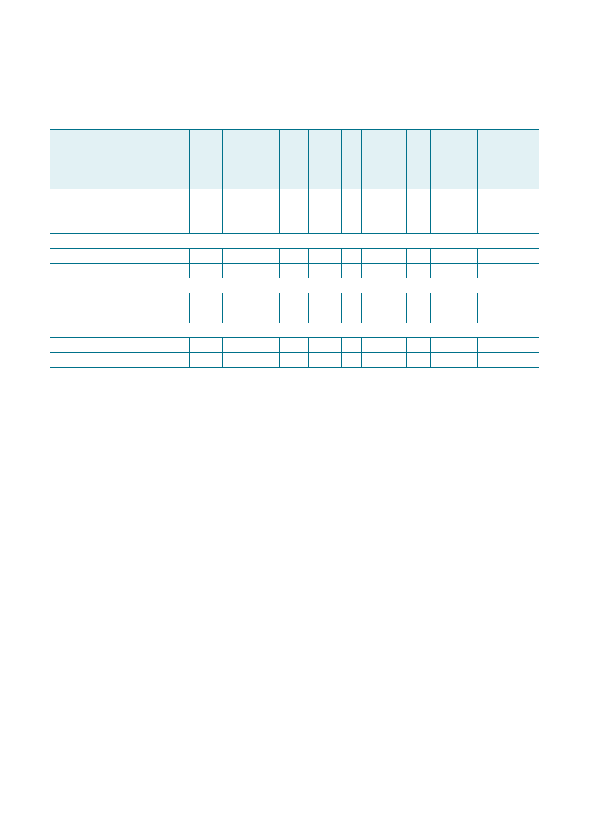
Table 1. Ordering information
Type number Package
LPC4088
LPC4088FBD208 LQFP208 plastic low profile quad flat package; 208 leads; body 28 28 1.4 mm SOT459-1
LPC4088FET208 TFBGA208 plastic thin fine-pitch ball grid array package; 208 balls; body
LPC4088FET180 TFBGA180 thin fine-pitch ball grid array package; 180 balls SOT570-3
LPC4088FBD144 LQFP144 plastic low profile quad flat package; 144 leads; body 20 20 1.4 mm SOT486-1
LPC4078
LPC4078FBD208 LQFP208 plastic low profile quad flat package; 208 leads; body 28 28 1.4 mm SOT459-1
LPC4078FET208 TFBGA208 plastic thin fine-pitch ball grid array package; 208 balls; body
LPC4078FET180 TFBGA180 thin fine-pitch ball grid array package; 180 balls SOT570-3
LPC4078FBD144 LQFP144 plastic low profile quad flat package; 144 leads; body 20 20 1.4 mm SOT486-1
LPC4078FBD80 LQFP80 plastic low-profile quad package; 80 leads; body 12 12 1.4 mm SOT315-1
LPC4078FBD100 LQFP100 plastic low profile quad flat package; 100 leads; body 14 14 1.4 mm SOT407-1
LPC4076
LPC4076FET180 TFBGA180 thin fine-pitch ball grid array package; 180 balls SOT570-3
LPC4076FBD144 LQFP144 plastic low profile quad flat package; 144 leads; body 20 20 1.4 mm SOT486-1
LPC4074
LPC4074FBD144 LQFP144 plastic low profile quad flat package; 144 leads; body 20 20 1.4 mm SOT486-1
LPC4074FBD80 LQFP80 plastic low-profile quad package; 80 leads; body 12 12 1.4 mm SOT315-1
LPC4072
LPC4072FET80 TFBGA80 plastic thin fine-pitch ball grid array package; 80 balls SOT1328-1
LPC4072FBD80 LQFP80 plastic low-profile quad package; 80 leads; body 12 12 1.4 mm SOT315-1
Name Description Version
SOT950-1
15 15 0.7 mm
SOT950-1
15 15 0.7 mm
Flash (kB)
SRAM (kB)
EEPROM (B)
EMC bus
width (bit)
LCD
Ethernet
USB
CAN
UART
QEI
SD/MMC
Comparator
FPU
Package
Table 2. Ordering options
Type number
LPC4088
LPC4088FBD208 512 96 4032 32 yes yes H/O/D 2 5 yes yes yes yes LQFP208
LPC4088FET208 512 96 4032 32 yes yes H/O/D 2 5 yes yes yes yes TFBGA208
LPC4088FET180 512 96 4032 16 yes yes H/O/D 2 5 yes yes yes yes TFBGA180
LPC4088FBD144 512 96 4032 8 yes yes H/O/D 2 5 yes yes yes yes LQFP144
LPC4078
LPC4078FBD208 512 96 4032 32 no yes H/O/D 2 5 yes yes yes yes LQFP208
LPC4078FET208 512 96 4032 32 no yes H/O/D 2 5 yes yes yes yes TFBGA208
LPC4078FET180 512 96 4032 16 no yes H/O/D 2 5 yes yes yes yes TFBGA180
LPC408X_7X All information provided in this document is subject to legal disclaimers. © NXP Semiconductors N.V. 2017. All rights reserved.
Product data sheet Rev. 3 — 11 January 2017 5 of 140
Page 6
NXP Semiconductors
LPC408x/7x
32-bit ARM Cortex-M4 microcontroller
Table 2. Ordering options
Type number
Flash (kB)
LPC4078FBD144 512 96 4032 8 no yes H/O/D 2 5 yes yes yes yes LQFP144
LPC4078FBD100 512 96 4032 - no yes H/O/D 2 5 yes yes yes yes LQFP100
LPC4078FBD80 512 96 4032 - no yes H/O/D 2 5 yes no yes yes LQFP80
LPC4076
LPC4076FET180 256 80 2048 16 no yes H/O/D 2 5 yes yes yes yes TFBGA180
LPC4076FBD144 256 80 2048 8 no yes H/O/D 2 5 yes yes yes yes LQFP144
LPC4074
LPC4074FBD144 128 40 2048 - no no D 2 4 no no no no LQFP144
LPC4074FBD80 128 40 2048 - no no D 2 4 no no no no LQFP80
LPC4072
LPC4072FET80 64 24 2048 - no no D 2 4 no no no no TFBGA80
LPC4072FBD80 64 24 2048 - no no D 2 4 no no no no LQFP80
…continued
SRAM (kB)
EEPROM (B)
EMC bus
width (bit)
LCD
Ethernet
USB
CAN
UART
QEI
SD/MMC
Comparator
FPU
Package
LPC408X_7X All information provided in this document is subject to legal disclaimers. © NXP Semiconductors N.V. 2017. All rights reserved.
Product data sheet Rev. 3 — 11 January 2017 6 of 140
Page 7
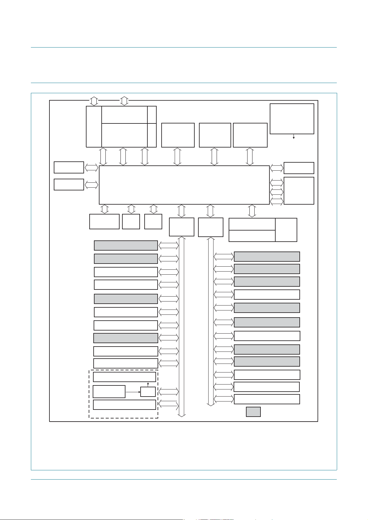
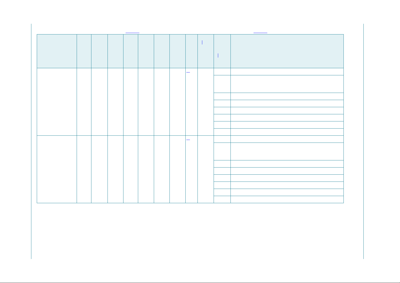
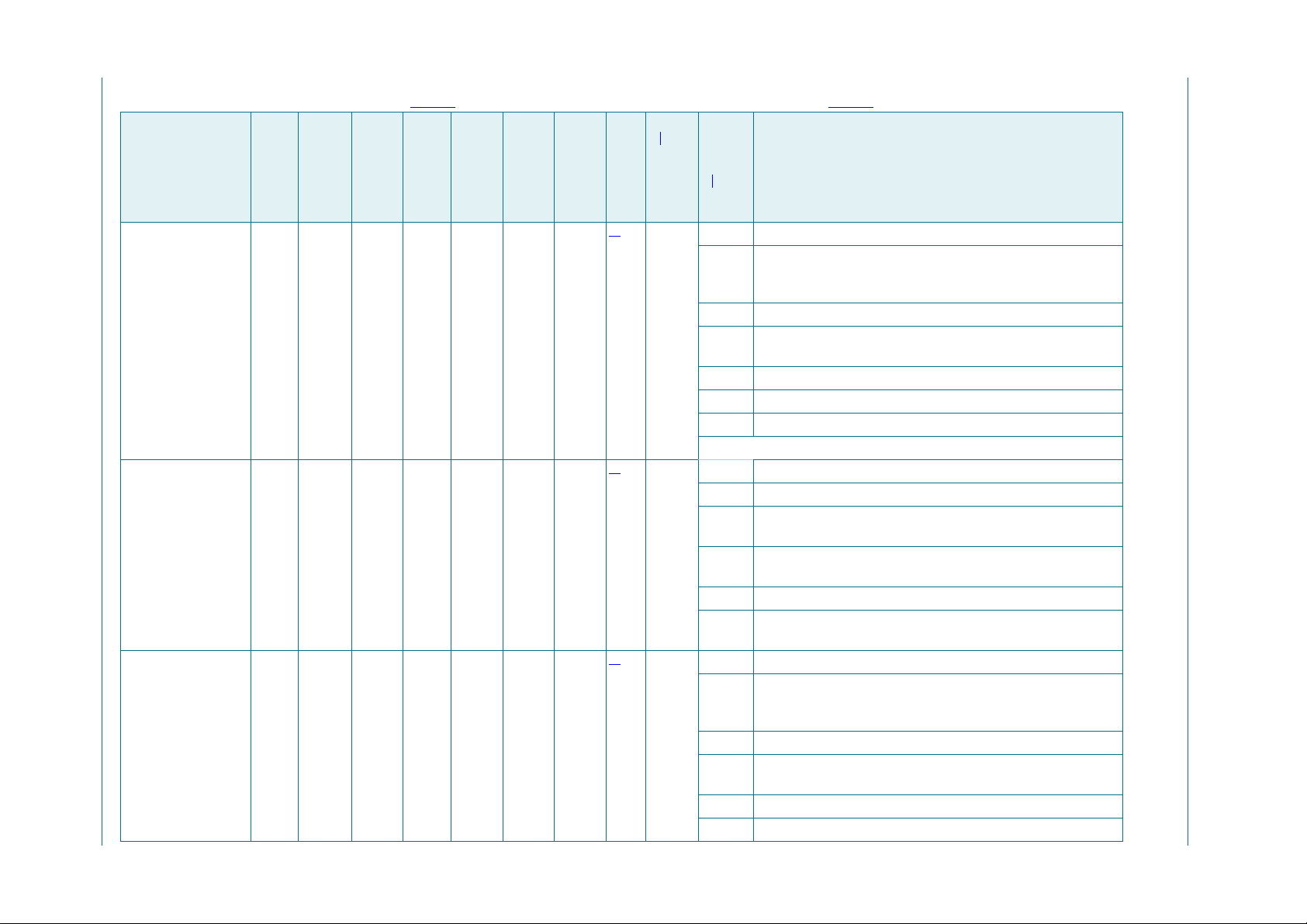
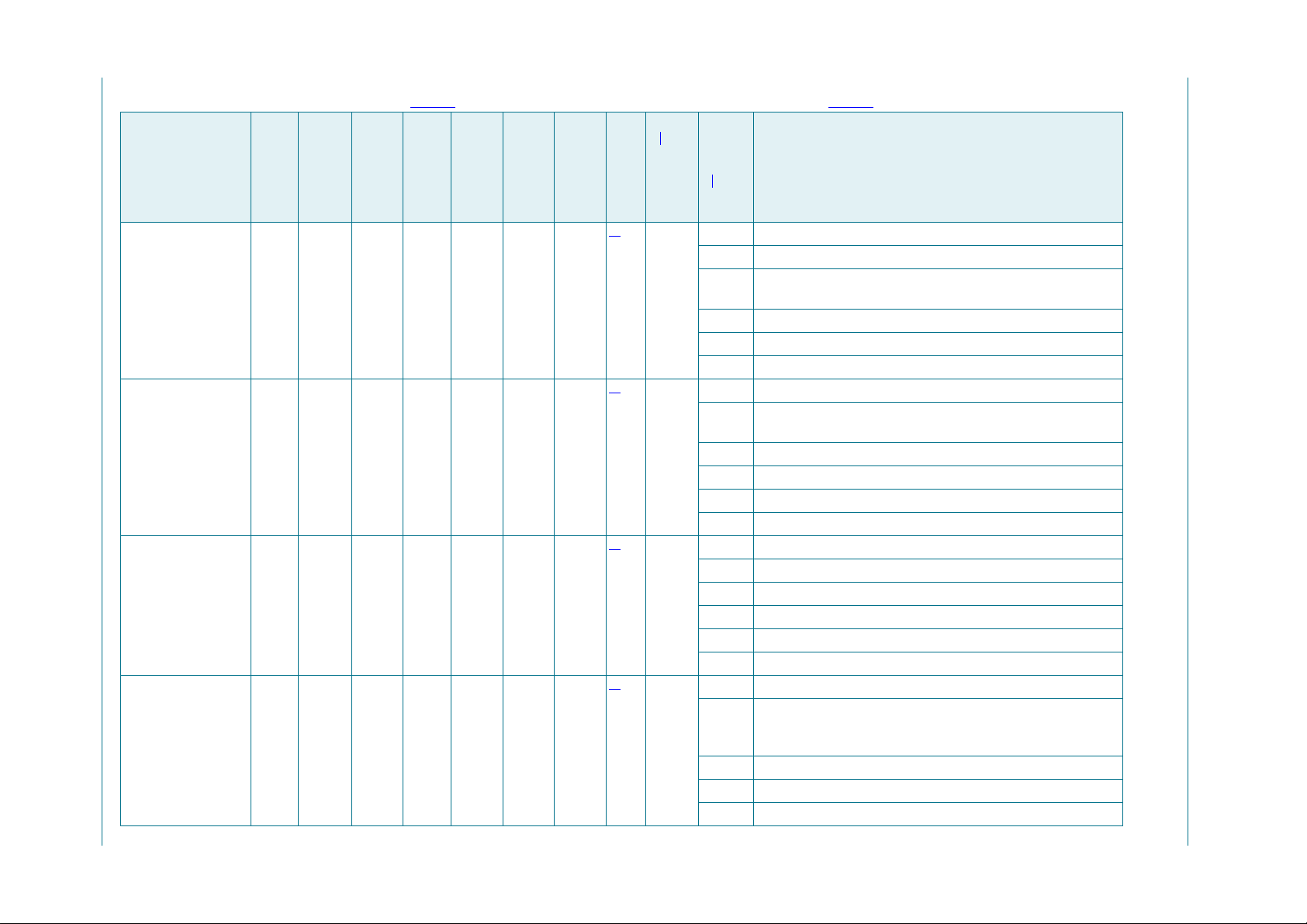
NXP Semiconductors
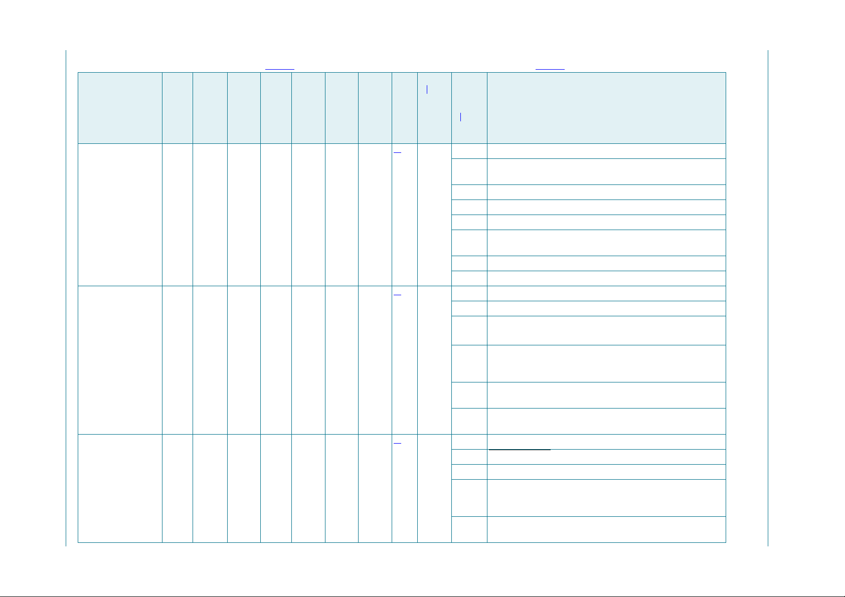
SRAM
96/80/
40/24 kB
ARM
CORTEX-M4
TEST/DEBUG
INTERFACE
EMULATION
TRACE MODULE
FLASH
ACCELERATOR
FLASH
512/256/128/64 kB
GPDMA
CONTROLLER
I-code
bus
D-code
bus
system
bus
AHB TO
APB
BRIDGE 0
HIGH-SPEED
GPIO
AHB TO
APB
BRIDGE 1
4032 B/
2048 B
EEPROM
CLOCK
GENERATION,
POWER CONTROL,
SYSTEM
FUNCTIONS
clocks and
controls
SSP0/2
USART4
(1)
UART2/3
SYSTEM CONTROL
2 x ANALOG COMPARATOR
(1)
SSP1
UART0/1
I2C0/1
CAN 0/1
TIMER 0/1
WINDOWED WDT
12-bit ADC
PWM0/1
PIN CONNECT
GPIO INTERRUPT CONTROL
RTC
BACKUP REGISTERS
EVENT RECORDER
32 kHz
OSCILLATOR
APB slave group 1
APB slave group 0
RTC POWER DOMAIN
LPC408x/7x
master
ETHERNET
(1)
master
USB
DEVICE/
HOST
(1)
/OTG
(1)
master
002aag491
slave
slave
CRC
slave
SPIFI
slave
slave
slave
slave
ROM
EMC
(1)
slaveslave
LCD
(1)
slave
MULTILAYER AHB MATRIX
I2C2
TIMER2/3
DAC
I2S
QUADRATURE ENCODER
(1)
MOTOR CONTROL PWM
MPU FPU
(1)
SD/MMC
(1)
= connected to GPDMA
5. Block diagram
LPC408x/7x
32-bit ARM Cortex-M4 microcontroller
(1) Not available on all parts.
Fig 1. Block diagram
LPC408X_7X All information provided in this document is subject to legal disclaimers. © NXP Semiconductors N.V. 2017. All rights reserved.
Product data sheet Rev. 3 — 11 January 2017 7 of 140
Page 8
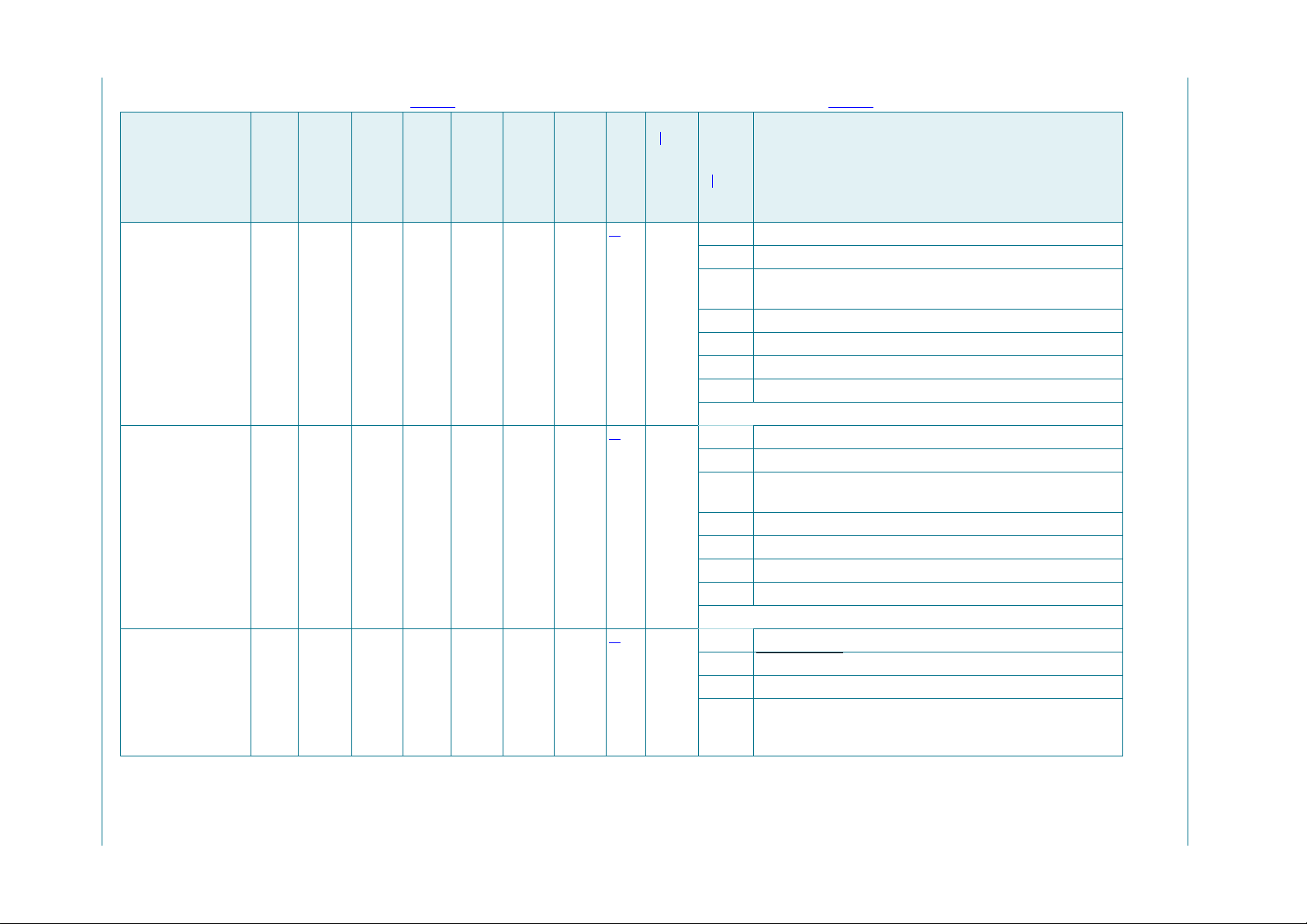
NXP Semiconductors
LPC408x/7x
156
53
104
208
157
105
1
52
002aag732
LPC408x/7x
108
37
72
144
109
73
1
36
002aag735
LPC407x
50
1
25
75
51
26
76
100
002aah638
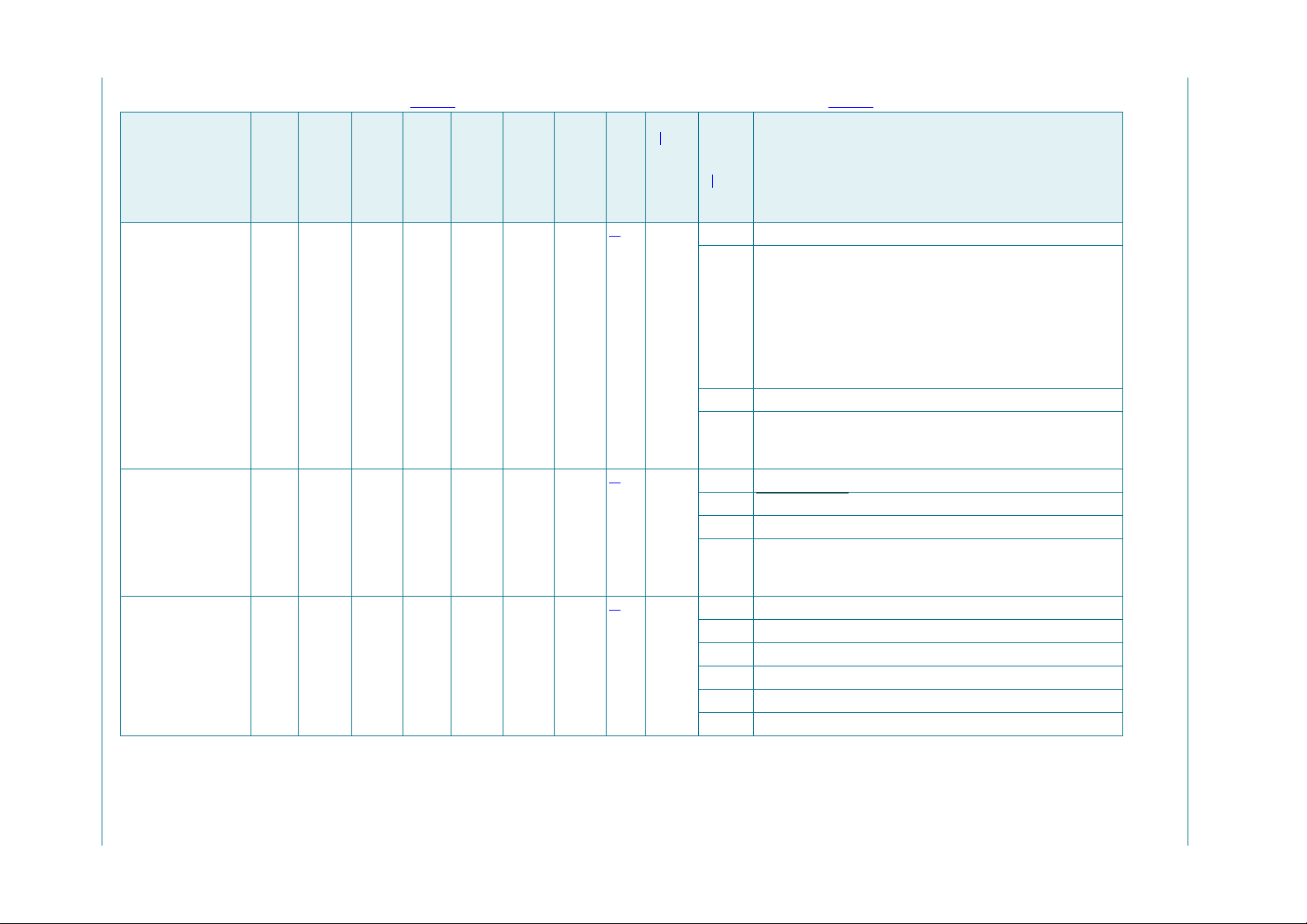
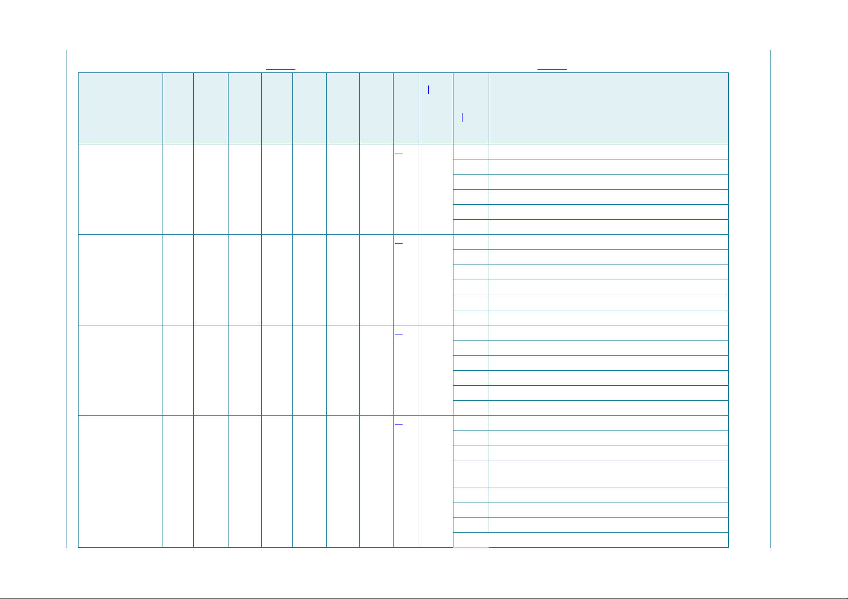
6. Pinning information
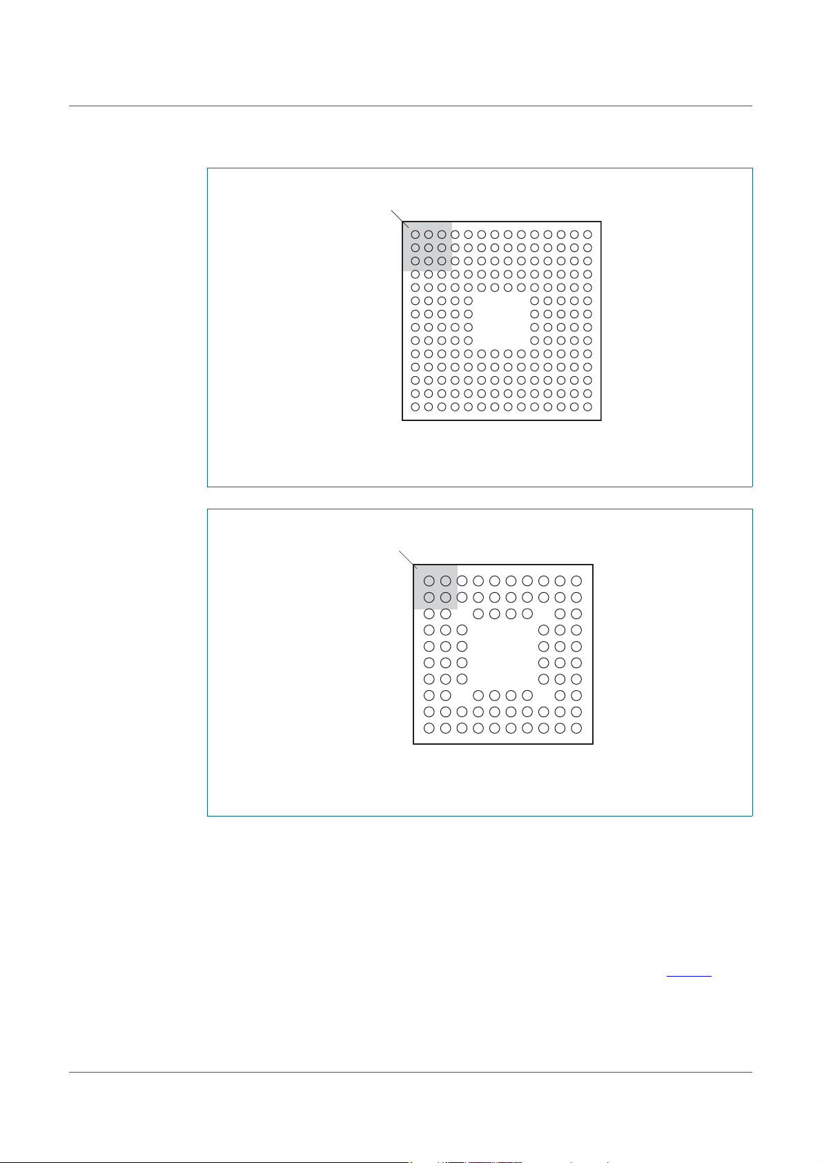
6.1 Pinning
Fig 2. Pin configuration (LQFP208)
LPC408x/7x
32-bit ARM Cortex-M4 microcontroller
Fig 3. Pin configuration (LQFP144)
Fig 4. Pin configuration (LQFP100)
LPC408X_7X All information provided in this document is subject to legal disclaimers. © NXP Semiconductors N.V. 2017. All rights reserved.
Product data sheet Rev. 3 — 11 January 2017 8 of 140
Page 9
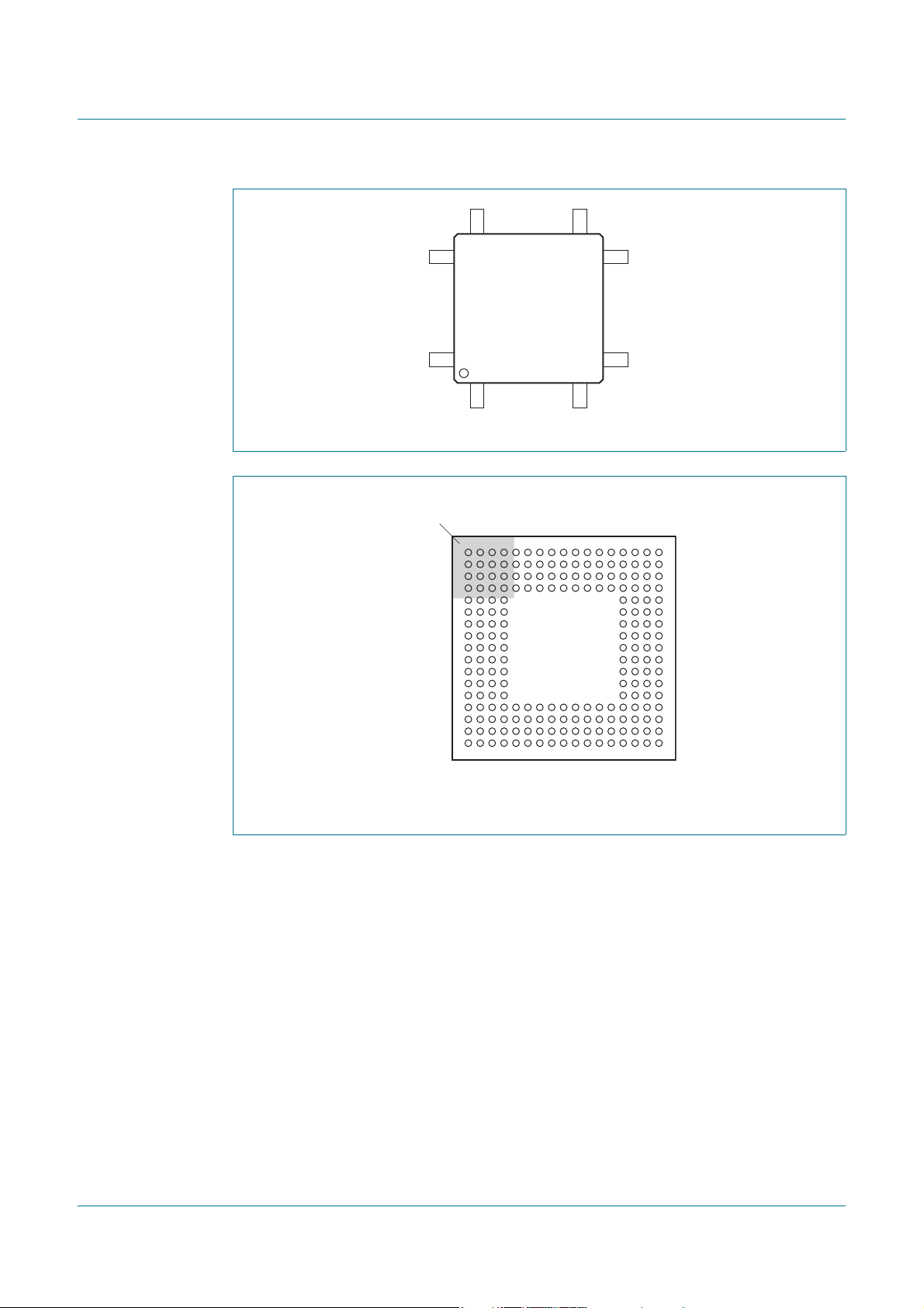
NXP Semiconductors
002aag733
LPC408x/7x
Transparent top view
ball A1
index area
U
T
R
P
N
M
K
H
L
J
G
F
E
D
C
A
B
246810121314
15 17
16
1357911
LPC408x/7x
32-bit ARM Cortex-M4 microcontroller
61
80
Fig 5. Pin configuration (LQFP80)
60
LPC408x/7x
1
41
20
40
21
002aag865
Fig 6. Pin configuration (TFBGA208)
LPC408X_7X All information provided in this document is subject to legal disclaimers. © NXP Semiconductors N.V. 2017. All rights reserved.
Product data sheet Rev. 3 — 11 January 2017 9 of 140
Page 10
NXP Semiconductors
002aag734
LPC408x/7x
2 4 6 8 10 12 13 141357911
ball A1
index area
P
N
M
L
K
J
G
E
H
F
D
C
B
A
Transparent top view
002aah684
LPC4072FET80
Transparent top view
12345678910
A
B
C
D
E
F
G
H
J
K
ball A1
index area
Fig 7. Pin configuration (TFBGA180)
LPC408x/7x
32-bit ARM Cortex-M4 microcontroller
Fig 8. Pin configuration (TFBGA80)
6.2 Pin description
I/O pins on the LPC408x/7x are 5 V tolerant and have input hysteresis unless otherwise
indicated in the table below. Crystal pins, power pins, and reference voltage pins are not
LPC408X_7X All information provided in this document is subject to legal disclaimers. © NXP Semiconductors N.V. 2017. All rights reserved.
Product data sheet Rev. 3 — 11 January 2017 10 of 140
5 V tolerant. In addition, when pins are selected to be ADC inputs, they are no longe r 5 V
tolerant and the input voltage must be limited to the volt a ge at the ADC positive refere nce
pin (VREFP).
All port pins Pn[m] are multiplexed, and the multiplexed functions appear in Table 3
order defined by the FUNC bits of the corresponding IOCON register up to the highest
used function number. Each port pin can support up to eight multiplexed functions.
IOCON register FUNC values which are reserved are noted as “R” in the pin configuration
table.
in the
Page 11
xxxxxxxxxxxxxxxxxxxxx xxxxxxxxxxxxxxxxxxxxxxxxxx xxxxxxx x x x xxxxxxxxxxxxxxxxxxxxxxxxxxxxxx xxxxxxxxxxxxxxxxxxx xx xx xxxxx
xxxxxxxxxxxxxxxxxxxxxxxxxxx xxxxxxxxxxxxxxxxxxx xxxxxx xxxxxxxxxxxxxxxxxxxxxxxxxxxxxxxxxxx xxxxxxxxxxxx x x
xxxxxxxxxxxxxxxxxxxxx xxxxxxxxxxxxxxxxxxxxxxxxxxxxxx xxxxx xxxxxxxxxxxxxxxxxxxxxxxxxxxxxxxxxxxxxxxxxxxxxxxxxx xxxxxxxx
LPC408X_7X All information provided in this document is subject to legal disclaimers. © NXP Semiconductors N.V. 2017. All rights reserved.
Product data sheet Rev. 3 — 11 January 2017 11 of 140
Table 3. Pin description
Not all functions are available on all parts. See Table 2 (Ethernet, USB, LCD, QEI, SD/MMC, comparator pins) and Table 5 (EMC pins).
Symbol
xxxxxxxxxxxxxxxxxxxxxxxxx xxxxxxxxxxxxxxxxxxxx xxx
Description
[1]
[2]
NXP Semiconductors
Pin LQFP208
Ball TFBGA208
Ball TFBGA180
Pin LQFP144
Pin LQFP100
Pin LQFP80
Pin TFBGA80
Reset state
Type
P0[0] to P0[31] I/O Port 0: Port 0 is a 32-bit I/O port with individual direction
controls for each bit. The operation of port 0 pins depends
upon the pin function selected via the pin connect block.
P0[0] 94U15M106646 37 J9
[3]
I; PU I/O P0[0] — General purpose digital input/output pin.
I CAN_RD1 — CAN1 receiver input.
O U3_TXD — Transmitter output for UART3.
2
I/O I2C1_SDA — I
C1 data input/output (this pin does not use
a specialized I2C pad).
O U0_TXD — Transmitter output for UART0.
[3]
P0[1] 96T14N116747 38 J10
I; PU I/O P0[1] — General purpose digital input/output pin.
O CAN_TD1 — CAN1 transmitter output.
I U3_RXD — Receiver input for UART3.
2
I/O I2C1_SCL — I
C1 clock input/output (this pin does not
use a specialized I2C pad).
I U0_RXD — Receiver input for UART0.
[3]
P0[2] 202 C4 D5 141 98 79 A2
I; PU I/O P0[2] — General purpose digital input/output pin.
O U0_TXD — Transmitter output for UART0.
O U3_TXD — Transmitter output for UART3.
[3]
P0[3] 204 D6 A3 142 99 80 A1
I; PU I/O P0[3] — General purpose digital input/output pin.
I U0_RXD — Receiver input for UART0.
I U3_RXD — Receiver input for UART3.
32-bit ARM Cortex-M4 microcontroller
LPC408x/7x
Page 12
xxxxxxxxxxxxxxxxxxxxx xxxxxxxxxxxxxxxxxxxxxxxxxx xxxxxxx x x x xxxxxxxxxxxxxxxxxxxxxxxxxxxxxx xxxxxxxxxxxxxxxxxxx xx xx xxxxx
xxxxxxxxxxxxxxxxxxxxxxxxxxx xxxxxxxxxxxxxxxxxxx xxxxxx xxxxxxxxxxxxxxxxxxxxxxxxxxxxxxxxxxx xxxxxxxxxxxx x x
xxxxxxxxxxxxxxxxxxxxx xxxxxxxxxxxxxxxxxxxxxxxxxxxxxx xxxxx xxxxxxxxxxxxxxxxxxxxxxxxxxxxxxxxxxxxxxxxxxxxxxxxxx xxxxxxxx
LPC408X_7X All information provided in this document is subject to legal disclaimers. © NXP Semiconductors N.V. 2017. All rights reserved.
Product data sheet Rev. 3 — 11 January 2017 12 of 140
Table 3. Pin description
Not all functions are available on all parts. See Table 2 (Ethernet, USB, LCD, QEI, SD/MMC, comparator pins) and Table 5 (EMC pins).
Symbol
xxxxxxxxxxxxxxxxxxxxxxxxx xxxxxxxxxxxxxxxxxxxx xxx
…continued
Description
[1]
[2]
NXP Semiconductors
Pin LQFP208
Ball TFBGA208
Ball TFBGA180
Pin LQFP144
Pin LQFP100
Pin LQFP80
P0[4] 168 B12 A11 116 81 - -
P0[5] 166 C12 B11 115 80 - -
Pin TFBGA80
[3]
Reset state
Type
I; PU I/O P0[4] — General purpose digital input/output pin.
2
I/O I2S_RX_SCK — I
S Receive clock. It is driven by the
master and received by the slave. Corresponds to the
signal SCK in the I2S-bus specification.
I CAN_RD2 — CAN2 receiver input.
I T2_CAP0 — Capture input for Timer 2, channel 0.
- R — Function reserved.
I/O CMP_ROSC — Comparator relaxation oscillator for 555
timer applications.
- R — Function reserved.
O LCD_VD[0] — LCD data.
[3]
I; PU I/O P0[5] — General purpose digital input/output pin.
2
I/O I2S_RX_WS — I
S Receive word select. It is driven by the
master and received by the slave. Corresponds to the
signal WS in the I2S-bus specification.
O CAN_TD2 — CAN2 transmitter output.
I T2_CAP1 — Capture input for Timer 2, channel 1.
32-bit ARM Cortex-M4 microcontroller
- R — Function reserved.
I CMP_RESET — Comparator reset.
- R — Function reserved.
O LCD_VD[1] — LCD data.
LPC408x/7x
Page 13
xxxxxxxxxxxxxxxxxxxxx xxxxxxxxxxxxxxxxxxxxxxxxxx xxxxxxx x x x xxxxxxxxxxxxxxxxxxxxxxxxxxxxxx xxxxxxxxxxxxxxxxxxx xx xx xxxxx
xxxxxxxxxxxxxxxxxxxxxxxxxxx xxxxxxxxxxxxxxxxxxx xxxxxx xxxxxxxxxxxxxxxxxxxxxxxxxxxxxxxxxxx xxxxxxxxxxxx x x
xxxxxxxxxxxxxxxxxxxxx xxxxxxxxxxxxxxxxxxxxxxxxxxxxxx xxxxx xxxxxxxxxxxxxxxxxxxxxxxxxxxxxxxxxxxxxxxxxxxxxxxxxx xxxxxxxx
LPC408X_7X All information provided in this document is subject to legal disclaimers. © NXP Semiconductors N.V. 2017. All rights reserved.
Product data sheet Rev. 3 — 11 January 2017 13 of 140
Table 3. Pin description
Not all functions are available on all parts. See Table 2 (Ethernet, USB, LCD, QEI, SD/MMC, comparator pins) and Table 5 (EMC pins).
Symbol
xxxxxxxxxxxxxxxxxxxxxxxxx xxxxxxxxxxxxxxxxxxxx xxx
…continued
Description
[1]
[2]
NXP Semiconductors
Pin LQFP208
Ball TFBGA208
Ball TFBGA180
Pin LQFP144
Pin LQFP100
Pin LQFP80
P0[6] 164 D13 D11 113 79 64 A7
P0[7] 162 C13 B12 112 78 63 A8
Pin TFBGA80
[3]
Reset state
Type
I; PU I/O P0[6] — General purpose digital input/output pin.
2
I/O I2S_RX_SDA — I
S Receive data. It is driven by the
transmitter and read by the receiver. Corresponds to the
signal SD in the I2S-bus specification.
I/O SSP1_SSEL — Slave Select for SSP1.
O T2_MAT0 — Match output for Timer 2, channel 0.
O U1_RTS — Request to Send output for UART1. Can also
be configured to be an RS-485/EIA-485 output enable
signal for UART1.
I/O CMP_ROSC — Comparator relaxation oscillator for 555
timer applications.
- R — Function reserved.
O LCD_VD[8] — LCD data.
[4]
I; IA I/O P0[7] — General purpose digital input/output pin.
2
I/O I2S_TX_SCK — I
S transmit clock. It is driven by the
master and received by the slave. Corresponds to the
2
signal SCK in the I
S-bus specification.
32-bit ARM Cortex-M4 microcontroller
I/O SSP1_SCK — Serial Clock for SSP1.
O T2_MAT1 — Match output for Timer 2, channel 1.
I RTC_EV0 — Event input 0 to Event Monitor/Recorder.
I CMP_VREF — Comparator reference voltage.
- R — Function reserved.
LPC408x/7x
O LCD_VD[9] — LCD data.
Page 14
xxxxxxxxxxxxxxxxxxxxx xxxxxxxxxxxxxxxxxxxxxxxxxx xxxxxxx x x x xxxxxxxxxxxxxxxxxxxxxxxxxxxxxx xxxxxxxxxxxxxxxxxxx xx xx xxxxx
xxxxxxxxxxxxxxxxxxxxxxxxxxx xxxxxxxxxxxxxxxxxxx xxxxxx xxxxxxxxxxxxxxxxxxxxxxxxxxxxxxxxxxx xxxxxxxxxxxx x x
xxxxxxxxxxxxxxxxxxxxx xxxxxxxxxxxxxxxxxxxxxxxxxxxxxx xxxxx xxxxxxxxxxxxxxxxxxxxxxxxxxxxxxxxxxxxxxxxxxxxxxxxxx xxxxxxxx
LPC408X_7X All information provided in this document is subject to legal disclaimers. © NXP Semiconductors N.V. 2017. All rights reserved.
Product data sheet Rev. 3 — 11 January 2017 14 of 140
Table 3. Pin description
Not all functions are available on all parts. See Table 2 (Ethernet, USB, LCD, QEI, SD/MMC, comparator pins) and Table 5 (EMC pins).
Symbol
xxxxxxxxxxxxxxxxxxxxxxxxx xxxxxxxxxxxxxxxxxxxx xxx
…continued
Description
[1]
[2]
NXP Semiconductors
Pin LQFP208
Ball TFBGA208
Ball TFBGA180
Pin LQFP144
Pin LQFP100
Pin LQFP80
P0[8] 160 A15 C12 111 77 62 A10
P0[9] 158 C14 A13 109 76 61 A9
Pin TFBGA80
[4]
Reset state
Type
I; IA I/O P0[8] — General purpose digital input/output pin.
2
I/O I2S_TX_WS — I
S Transmit word select. It is driven by the
master and received by the slave. Corresponds to the
signal WS in the I2S-bus specification.
I/O SSP1_MISO — Master In Slave Out for SSP1.
O T2_MAT2 — Match output for Timer 2, channel 2.
I RTC_EV1 — Event input 1 to Event Monitor/Recorder.
I CMP1_IN[3] — Comparator 1, input 3.
- R — Function reserved.
O LCD_VD[16] — LCD data.
[4]
I; IA I/O P0[9] — General purpose digital input/output pin.
2
I/O I2S_TX_SDA — I
S transmit data. It is driven by the
transmitter and read by the receiver. Corresponds to the
2
signal SD in the I
S-bus specification.
I/O SSP1_MOSI — Master Out Slave In for SSP1.
O T2_MAT3 — Match output for Timer 2, channel 3.
32-bit ARM Cortex-M4 microcontroller
I RTC_EV2 — Event input 2 to Event Monitor/Recorder.
I CMP1_IN[2] — Comparator 1, input 2.
- R — Function reserved.
O LCD_VD[17] — LCD data.
LPC408x/7x
Page 15
xxxxxxxxxxxxxxxxxxxxx xxxxxxxxxxxxxxxxxxxxxxxxxx xxxxxxx x x x xxxxxxxxxxxxxxxxxxxxxxxxxxxxxx xxxxxxxxxxxxxxxxxxx xx xx xxxxx
xxxxxxxxxxxxxxxxxxxxxxxxxxx xxxxxxxxxxxxxxxxxxx xxxxxx xxxxxxxxxxxxxxxxxxxxxxxxxxxxxxxxxxx xxxxxxxxxxxx x x
xxxxxxxxxxxxxxxxxxxxx xxxxxxxxxxxxxxxxxxxxxxxxxxxxxx xxxxx xxxxxxxxxxxxxxxxxxxxxxxxxxxxxxxxxxxxxxxxxxxxxxxxxx xxxxxxxx
LPC408X_7X All information provided in this document is subject to legal disclaimers. © NXP Semiconductors N.V. 2017. All rights reserved.
Product data sheet Rev. 3 — 11 January 2017 15 of 140
Table 3. Pin description
Not all functions are available on all parts. See Table 2 (Ethernet, USB, LCD, QEI, SD/MMC, comparator pins) and Table 5 (EMC pins).
Symbol
xxxxxxxxxxxxxxxxxxxxxxxxx xxxxxxxxxxxxxxxxxxxx xxx
…continued
Description
[1]
[2]
NXP Semiconductors
Pin LQFP208
Ball TFBGA208
Ball TFBGA180
Pin LQFP144
Pin LQFP100
Pin LQFP80
P0[10] 98 T15 L10 69 48 39 K9
P0[11] 100 R14 P12 70 49 40 K10
P0[12] 41 R1 J4 29 - - -
Pin TFBGA80
[3]
Reset state
Type
I; PU I/O P0[10] — General purpose digital input/output pin.
O U2_TXD — Transmitter output for UART2.
2
I/O I2C2_SDA — I
C2 data input/output (this pin does not use
a specialized I2C pad).
O T3_MAT0 — Match output for Timer 3, channel 0.
- R — Function reserved.
- R — Function reserved.
- R — Function reserved.
O LCD_VD[5] — LCD data.
[3]
I; PU I/O P0[11] — General purpose digital input/output pin.
I U2_RXD — Receiver input for UART2.
2
I/O I2C2_SCL — I
C2 clock input/output (this pin does not
use a specialized I2C pad).
O T3_MAT1 — Match output for Timer 3, channel 1.
- R — Function reserved.
- R — Function reserved.
32-bit ARM Cortex-M4 microcontroller
- R — Function reserved.
O LCD_VD[10] — LCD data.
[5]
I; PU I/O P0[12] — General purpose digital input/output pin.
O USB_PPWR2
— Port Power enable signal for USB port 2.
LPC408x/7x
I/O SSP1_MISO — Master In Slave Out for SSP1.
I ADC0_IN[6] — A/D converter 0, input 6. When configured
as an ADC input, the digital function of the pin must be
disabled.
Page 16
xxxxxxxxxxxxxxxxxxxxx xxxxxxxxxxxxxxxxxxxxxxxxxx xxxxxxx x x x xxxxxxxxxxxxxxxxxxxxxxxxxxxxxx xxxxxxxxxxxxxxxxxxx xx xx xxxxx
xxxxxxxxxxxxxxxxxxxxxxxxxxx xxxxxxxxxxxxxxxxxxx xxxxxx xxxxxxxxxxxxxxxxxxxxxxxxxxxxxxxxxxx xxxxxxxxxxxx x x
xxxxxxxxxxxxxxxxxxxxx xxxxxxxxxxxxxxxxxxxxxxxxxxxxxx xxxxx xxxxxxxxxxxxxxxxxxxxxxxxxxxxxxxxxxxxxxxxxxxxxxxxxx xxxxxxxx
LPC408X_7X All information provided in this document is subject to legal disclaimers. © NXP Semiconductors N.V. 2017. All rights reserved.
Product data sheet Rev. 3 — 11 January 2017 16 of 140
Table 3. Pin description
Not all functions are available on all parts. See Table 2 (Ethernet, USB, LCD, QEI, SD/MMC, comparator pins) and Table 5 (EMC pins).
Symbol
xxxxxxxxxxxxxxxxxxxxxxxxx xxxxxxxxxxxxxxxxxxxx xxx
…continued
Description
[1]
[2]
NXP Semiconductors
Pin LQFP208
P0[13] 45 R2 J5 32 - - -
P0[14] 69 T7 M5 48 - - -
P0[15] 128 J16 H13 89 62 47 F9
Ball TFBGA208
Ball TFBGA180
Pin LQFP144
Pin LQFP100
Pin LQFP80
Pin TFBGA80
[5]
[3]
[3]
Reset state
I; PU I/O P0[13] — General purpose digital input/output pin.
I; PU I/O P0[14] — General purpose digital input/output pin.
I; PU I/O P0[15] — General purpose digital input/output pin.
Type
O USB_UP_LED2 — USB port 2 GoodLink LED indicator. It
is LOW when the device is configured (non-control
endpoints enabled), or when the host is enabled and has
detected a device on the bus. It is HIGH when the device
is not configured, or when host is enabled and has not
detected a device on the bus, or during global suspend. It
transitions between LOW and HIGH (flashes) when the
host is enabled and detects activity on the bus.
I/O SSP1_MOSI — Master Out Slave In for SSP1.
I ADC0_IN[7] — A/D converter 0, input 7. When configured
as an ADC input, the digital function of the pin must be
disabled.
O USB_HSTEN2
I/O SSP1_SSEL — Slave Select for SSP1.
O USB_CONNECT2 — SoftConnect control for USB port 2.
Signal used to switch an external 1.5 k resistor under
software control. Used with the SoftConnect USB feature.
O U1_TXD — Transmitter output for UART1.
I/O SSP0_SCK — Serial clock for SSP0.
- R — Function reserved.
- R — Function reserved.
I/O SPIFI_IO[2] — Data bit 0 for SPIFI.
— Host Enabled status for USB port 2.
32-bit ARM Cortex-M4 microcontroller
LPC408x/7x
Page 17
xxxxxxxxxxxxxxxxxxxxx xxxxxxxxxxxxxxxxxxxxxxxxxx xxxxxxx x x x xxxxxxxxxxxxxxxxxxxxxxxxxxxxxx xxxxxxxxxxxxxxxxxxx xx xx xxxxx
xxxxxxxxxxxxxxxxxxxxxxxxxxx xxxxxxxxxxxxxxxxxxx xxxxxx xxxxxxxxxxxxxxxxxxxxxxxxxxxxxxxxxxx xxxxxxxxxxxx x x
xxxxxxxxxxxxxxxxxxxxx xxxxxxxxxxxxxxxxxxxxxxxxxxxxxx xxxxx xxxxxxxxxxxxxxxxxxxxxxxxxxxxxxxxxxxxxxxxxxxxxxxxxx xxxxxxxx
LPC408X_7X All information provided in this document is subject to legal disclaimers. © NXP Semiconductors N.V. 2017. All rights reserved.
Product data sheet Rev. 3 — 11 January 2017 17 of 140
Table 3. Pin description
Not all functions are available on all parts. See Table 2 (Ethernet, USB, LCD, QEI, SD/MMC, comparator pins) and Table 5 (EMC pins).
Symbol
xxxxxxxxxxxxxxxxxxxxxxxxx xxxxxxxxxxxxxxxxxxxx xxx
…continued
Description
[1]
[2]
NXP Semiconductors
Pin LQFP208
Ball TFBGA208
Ball TFBGA180
Pin LQFP144
Pin LQFP100
Pin LQFP80
Pin TFBGA80
P0[16] 130 J14 H14 90 63 48 F8
P0[17] 126 K17 J12 87 61 46 F10
P0[18] 124 K15 J13 86 60 45 G10
P0[19] 122 L17 J10 85 59 - -
[3]
Reset state
I; PU I/O P0[16] — General purpose digital input/output pin.
Type
I U1_RXD — Receiver input for UART1.
I/O SSP0_SSEL — Slave Select for SSP0.
- R — Function reserved.
- R — Function reserved.
I/O SPIFI_IO[3] — Data bit 0 for SPIFI.
[3]
I; PU I/O P0[17] — General purpose digital input/output pin.
I U1_CTS — Clear to Send input for UART1.
I/O SSP0_MISO — Master In Slave Out for SSP0.
- R — Function reserved.
- R — Function reserved.
I/O SPIFI_IO[1] — Data bit 0 for SPIFI.
[3]
I; PU I/O P0[18] — General purpose digital input/output pin.
I U1_DCD — Data Carrier Detect input for UART1.
I/O SSP0_MOSI — Master Out Slave In for SSP0.
- R — Function reserved.
- R — Function reserved.
I/O SPIFI_IO[0] — Data bit 0 for SPIFI.
[3]
I; PU I/O P0[19] — General purpose digital input/output pin.
I U1_DSR — Data Set Ready input for UART1.
O SD_CLK — Clock output line for SD card interface.
2
I/O I2C1_SDA — I
C1 data input/output (this pin does not use
a specialized I2C pad).
- R — Function reserved.
- R — Function reserved.
- R — Function reserved.
O LCD_VD[13] — LCD data.
32-bit ARM Cortex-M4 microcontroller
LPC408x/7x
Page 18
xxxxxxxxxxxxxxxxxxxxx xxxxxxxxxxxxxxxxxxxxxxxxxx xxxxxxx x x x xxxxxxxxxxxxxxxxxxxxxxxxxxxxxx xxxxxxxxxxxxxxxxxxx xx xx xxxxx
xxxxxxxxxxxxxxxxxxxxxxxxxxx xxxxxxxxxxxxxxxxxxx xxxxxx xxxxxxxxxxxxxxxxxxxxxxxxxxxxxxxxxxx xxxxxxxxxxxx x x
xxxxxxxxxxxxxxxxxxxxx xxxxxxxxxxxxxxxxxxxxxxxxxxxxxx xxxxx xxxxxxxxxxxxxxxxxxxxxxxxxxxxxxxxxxxxxxxxxxxxxxxxxx xxxxxxxx
LPC408X_7X All information provided in this document is subject to legal disclaimers. © NXP Semiconductors N.V. 2017. All rights reserved.
Product data sheet Rev. 3 — 11 January 2017 18 of 140
Table 3. Pin description
Not all functions are available on all parts. See Table 2 (Ethernet, USB, LCD, QEI, SD/MMC, comparator pins) and Table 5 (EMC pins).
Symbol
xxxxxxxxxxxxxxxxxxxxxxxxx xxxxxxxxxxxxxxxxxxxx xxx
…continued
Description
[1]
[2]
NXP Semiconductors
Pin LQFP208
Ball TFBGA208
Ball TFBGA180
Pin LQFP144
Pin LQFP100
Pin LQFP80
Pin TFBGA80
P0[20] 120 M17 K14 83 58 - -
P0[21] 118 M16 K11 82 57 - -
P0[22] 1 16 N17 L14 80 56 44 H10
[3]
Reset state
I; PU I/O P0[20] — General purpose digital input/output pin.
Type
O U1_DTR — Data Terminal Ready output for UART1. Can
also be configured to be an RS-485/EIA-485 output enable
signal for UART1.
I/O SD_CMD — Command line for SD card interface.
2
I/O I2C1_SCL — I
C1 clock input/output (this pin does not
use a specialized I2C pad).
- R — Function reserved.
- R — Function reserved.
- R — Function reserved.
O LCD_VD[14] — LCD data.
[3]
I; PU I/O P0[21] — General purpose digital input/output pin.
I U1_RI — Ring Indicator input for UART1.
O SD_PWR — Power Supply Enable for external SD card
power supply.
O U4_OE — RS-485/EIA-485 output enable signal for
UART4.
I CAN_RD1 — CAN1 receiver input.
I/O U4_SCLK — USART 4 clock input or output in
synchronous mode.
[6]
I; PU I/O P0[22] — General purpose digital input/output pin.
O U1_RTS — Request to Send output for UART1. Can also
be configured to be an RS-485/EIA-485 output enable
signal for UART1.
I/O SD_DAT[0] — Data line 0 for SD card interface.
O U4_TXD — Transmitter output for USART4 (input/output
in smart card mode).
O CAN_TD1 — CAN1 transmitter output.
O SPIFI_CLK — Clock output for SPIFI.
32-bit ARM Cortex-M4 microcontroller
LPC408x/7x
Page 19
xxxxxxxxxxxxxxxxxxxxx xxxxxxxxxxxxxxxxxxxxxxxxxx xxxxxxx x x x xxxxxxxxxxxxxxxxxxxxxxxxxxxxxx xxxxxxxxxxxxxxxxxxx xx xx xxxxx
xxxxxxxxxxxxxxxxxxxxxxxxxxx xxxxxxxxxxxxxxxxxxx xxxxxx xxxxxxxxxxxxxxxxxxxxxxxxxxxxxxxxxxx xxxxxxxxxxxx x x
xxxxxxxxxxxxxxxxxxxxx xxxxxxxxxxxxxxxxxxxxxxxxxxxxxx xxxxx xxxxxxxxxxxxxxxxxxxxxxxxxxxxxxxxxxxxxxxxxxxxxxxxxx xxxxxxxx
LPC408X_7X All information provided in this document is subject to legal disclaimers. © NXP Semiconductors N.V. 2017. All rights reserved.
Product data sheet Rev. 3 — 11 January 2017 19 of 140
Table 3. Pin description
Not all functions are available on all parts. See Table 2 (Ethernet, USB, LCD, QEI, SD/MMC, comparator pins) and Table 5 (EMC pins).
Symbol
xxxxxxxxxxxxxxxxxxxxxxxxx xxxxxxxxxxxxxxxxxxxx xxx
…continued
Description
[1]
[2]
NXP Semiconductors
Pin LQFP208
Ball TFBGA208
Ball TFBGA180
Pin LQFP144
Pin LQFP100
Pin LQFP80
P0[23] 18 H1 F5 13 9 - -
P0[24] 16 G2 E1 11 8 - -
P0[25] 14 F1 E4 10 7 7 D1
Pin TFBGA80
[5]
Reset state
Type
I; PU I/O P0[23] — General purpose digital input/output pin.
I ADC0_IN[0] — A/D converter 0, input 0. When configured
as an ADC input, the digital function of the pin must be
disabled.
I/O I2S_RX_SCK — Receive Clock. It is driven by the master
and received by the slave. Corresponds to the signal SCK
2
in the I
S-bus specification.
I T3_CAP0 — Capture input for Timer 3, channel 0.
[5]
I; PU I/O P0[24] — General purpose digital input/output pin.
I ADC0_IN[1] — A/D converter 0, input 1. When configured
as an ADC input, the digital function of the pin must be
disabled.
I/O I2S_RX_WS — Receive Word Select. It is driven by the
master and received by the slave. Corresponds to the
2
signal WS in the I
S-bus specification.
I T3_CAP1 — Capture input for Timer 3, channel 1.
[5]
I; PU I/O P0[25] — General purpose digital input/output pin.
32-bit ARM Cortex-M4 microcontroller
I ADC0_IN[2] — A/D converter 0, input 2. When configured
as an ADC input, the digital function of the pin must be
disabled.
I/O I2S_RX_SDA — Receive data. It is driven by the
transmitter and read by the receiver. Corresponds to the
signal SD in the I
2
S-bus specification.
LPC408x/7x
O U3_TXD — Transmitter output for UART3.
Page 20
xxxxxxxxxxxxxxxxxxxxx xxxxxxxxxxxxxxxxxxxxxxxxxx xxxxxxx x x x xxxxxxxxxxxxxxxxxxxxxxxxxxxxxx xxxxxxxxxxxxxxxxxxx xx xx xxxxx
xxxxxxxxxxxxxxxxxxxxxxxxxxx xxxxxxxxxxxxxxxxxxx xxxxxx xxxxxxxxxxxxxxxxxxxxxxxxxxxxxxxxxxx xxxxxxxxxxxx x x
xxxxxxxxxxxxxxxxxxxxx xxxxxxxxxxxxxxxxxxxxxxxxxxxxxx xxxxx xxxxxxxxxxxxxxxxxxxxxxxxxxxxxxxxxxxxxxxxxxxxxxxxxx xxxxxxxx
LPC408X_7X All information provided in this document is subject to legal disclaimers. © NXP Semiconductors N.V. 2017. All rights reserved.
Product data sheet Rev. 3 — 11 January 2017 20 of 140
Table 3. Pin description
Not all functions are available on all parts. See Table 2 (Ethernet, USB, LCD, QEI, SD/MMC, comparator pins) and Table 5 (EMC pins).
Symbol
xxxxxxxxxxxxxxxxxxxxxxxxx xxxxxxxxxxxxxxxxxxxx xxx
…continued
Description
[1]
[2]
NXP Semiconductors
Pin LQFP208
P0[26] 12 E1 D1 8 6 6 D2
Ball TFBGA208
Ball TFBGA180
Pin LQFP144
Pin LQFP100
Pin LQFP80
Pin TFBGA80
[7]
Reset state
Type
I; PU I/O P0[26] — General purpose digital input/output pin.
I ADC0_IN[3] — A/D converter 0, input 3. When configured
as an ADC input, the digital function of the pin must be
disabled.
O DAC_OUT — D/A converter output. When configured as
the DAC output, the digital function of the pin must be
disabled.
I U3_RXD — Receiver input for UART3.
[8]
P0[27] 50 T1 L3 35 25 - -
I I/O P0[27] — General purpose digital input/output pin.
2
I/O I2C0_SDA — I
C0 data input/output. (This pin uses a
specialized I2C pad).
I/O USB_SDA1 — I2C serial data for communication with an
external USB transceiver.
[8]
P0[28] 48 R3 M1 34 24 - -
I I/O P0[28] — General purpose digital input/output pin.
2
I/O I2C0_SCL — I
C0 clock input/output (this pin uses a
specialized I2C pad.
I/O USB_SCL1 — I2C serial clock for communication with an
external USB transceiver.
[9]
P0[29] 61 U4 K5 42 29 22 J3
I I/O P0[29] — General purpose digital input/output pin.
I/O USB_D+1 — USB port 1 bidirectional D+ line.
— External interrupt 0 input.
P0[30] 62 R6 N4 43 30 23 K3
I EINT0
[9]
I I/O P0[30] — General purpose digital input/output pin.
I/O USB_D1 — USB port 1 bidirectional D line.
— External interrupt 1 input.
P0[31] 51 T2 N1 36 - - -
I EINT1
[9]
I I/O P0[31] — General purpose digital input/output pin.
I/O USB_D+2 — USB port 2 bidirectional D+ line.
P1[0] to P1[31] I/O Port 1: Port 1 is a 32 bit I/O port with individual direction
controls for each bit. The operation of port 1 pins depends
upon the pin function selected via the pin connect block
32-bit ARM Cortex-M4 microcontroller
LPC408x/7x
Page 21
xxxxxxxxxxxxxxxxxxxxx xxxxxxxxxxxxxxxxxxxxxxxxxx xxxxxxx x x x xxxxxxxxxxxxxxxxxxxxxxxxxxxxxx xxxxxxxxxxxxxxxxxxx xx xx xxxxx
xxxxxxxxxxxxxxxxxxxxxxxxxxx xxxxxxxxxxxxxxxxxxx xxxxxx xxxxxxxxxxxxxxxxxxxxxxxxxxxxxxxxxxx xxxxxxxxxxxx x x
xxxxxxxxxxxxxxxxxxxxx xxxxxxxxxxxxxxxxxxxxxxxxxxxxxx xxxxx xxxxxxxxxxxxxxxxxxxxxxxxxxxxxxxxxxxxxxxxxxxxxxxxxx xxxxxxxx
LPC408X_7X All information provided in this document is subject to legal disclaimers. © NXP Semiconductors N.V. 2017. All rights reserved.
Product data sheet Rev. 3 — 11 January 2017 21 of 140
Table 3. Pin description
Not all functions are available on all parts. See Table 2 (Ethernet, USB, LCD, QEI, SD/MMC, comparator pins) and Table 5 (EMC pins).
Symbol
xxxxxxxxxxxxxxxxxxxxxxxxx xxxxxxxxxxxxxxxxxxxx xxx
…continued
Description
[1]
[2]
NXP Semiconductors
Pin LQFP208
Ball TFBGA208
Ball TFBGA180
Pin LQFP144
Pin LQFP100
Pin LQFP80
P1[0] 196 A3 B5 136 95 76 A3
P1[1] 194 B5 A5 135 94 75 B4
P1[2] 185 D9 B7 - - - -
P1[3] 177 A10 A9 - - - -
P1[4] 192 A5 C6 133 93 74 B5
Pin TFBGA80
[3]
Reset state
Type
I; PU I/O P1[0] — General purpose digital input/output pin.
O ENET_TXD0 — Ethernet transmit data 0 (RMII/MII
interface).
- R — Function reserved.
I T3_CAP1 — Capture input for Timer 3, channel 1.
I/O SSP2_SCK — Serial clock for SSP2.
[3]
I; PU I/O P1[1] — General purpose digital input/output pin.
O ENET_TXD1 — Ethernet transmit data 1 (RMII/MII
interface).
- R — Function reserved.
O T3_MAT3 — Match output for Timer 3, channel 3.
I/O SSP2_MOSI — Master Out Slave In for SSP2.
[3]
I; PU I/O P1[2] — General purpose digital input/output pin.
O ENET_TXD2 — Ethernet transmit data 2 (MII interface).
O SD_CLK — Clock output line for SD card interface.
O PWM0[1] — Pulse Width Modulator 0, output 1.
[3]
I; PU I/O P1[3] — General purpose digital input/output pin.
32-bit ARM Cortex-M4 microcontroller
O ENET_TXD3 — Ethernet transmit data 3 (MII interface).
I/O SD_CMD — Command line for SD card interface.
O PWM0[2] — Pulse Width Modulator 0, output 2.
[3]
I; PU I/O P1[4] — General purpose digital input/output pin.
LPC408x/7x
O ENET_TX_EN — Ethernet transmit data enable (RMII/MII
interface).
- R — Function reserved.
O T3_MAT2 — Match output for Timer 3, channel 2.
I/O SSP2_MISO — Master In Slave Out for SSP2.
Page 22
xxxxxxxxxxxxxxxxxxxxx xxxxxxxxxxxxxxxxxxxxxxxxxx xxxxxxx x x x xxxxxxxxxxxxxxxxxxxxxxxxxxxxxx xxxxxxxxxxxxxxxxxxx xx xx xxxxx
xxxxxxxxxxxxxxxxxxxxxxxxxxx xxxxxxxxxxxxxxxxxxx xxxxxx xxxxxxxxxxxxxxxxxxxxxxxxxxxxxxxxxxx xxxxxxxxxxxx x x
xxxxxxxxxxxxxxxxxxxxx xxxxxxxxxxxxxxxxxxxxxxxxxxxxxx xxxxx xxxxxxxxxxxxxxxxxxxxxxxxxxxxxxxxxxxxxxxxxxxxxxxxxx xxxxxxxx
LPC408X_7X All information provided in this document is subject to legal disclaimers. © NXP Semiconductors N.V. 2017. All rights reserved.
Product data sheet Rev. 3 — 11 January 2017 22 of 140
Table 3. Pin description
Not all functions are available on all parts. See Table 2 (Ethernet, USB, LCD, QEI, SD/MMC, comparator pins) and Table 5 (EMC pins).
Symbol
xxxxxxxxxxxxxxxxxxxxxxxxx xxxxxxxxxxxxxxxxxxxx xxx
…continued
Description
[1]
[2]
NXP Semiconductors
Pin LQFP208
Ball TFBGA208
Ball TFBGA180
Pin LQFP144
Pin LQFP100
Pin LQFP80
P1[5] 156 A17 B13 - - - -
P1[6] 171 B11 B10 - - - -
P1[7] 153 D14 C13 - - - -
P1[8] 190 C7 B6 132 92 73 C5
Pin TFBGA80
[3]
Reset state
Type
I; PU I/O P1[5] — General purpose digital input/output pin.
O ENET_TX_ER — Ethernet Transmit Error (MII interface).
O SD_PWR — Power Supply Enable for external SD card
power supply.
O PWM0[3] — Pulse Width Modulator 0, output 3.
- R — Function reserved.
I CMP1_IN[1] — Comparator 1, input 1.
[3]
I; PU I/O P1[6] — General purpose digital input/output pin.
I ENET_TX_CLK — Ethernet Transmit Clock (MII
interface).
I/O SD_DAT[0] — Data line 0 for SD card interface.
O PWM0[4] — Pulse Width Modulator 0, output 4.
- R — Function reserved.
I CMP0_IN[3] — Comparator 0, input 3.
[3]
I; PU I/O P1[7] — General purpose digital input/output pin.
I ENET_COL — Ethernet Collision detect (MII interface).
32-bit ARM Cortex-M4 microcontroller
I/O SD_DAT[1] — Data line 1 for SD card interface.
O PWM0[5] — Pulse Width Modulator 0, output 5.
- R — Function reserved.
I CMP1_IN[0] — Comparator 1, input 0.
[3]
I; PU I/O P1[8] — General purpose digital input/output pin.
LPC408x/7x
I ENET_CRS (ENET_CRS_DV) — Ethernet Carrier Sense
(MII interface) or Ethernet Carrier Sense/Data Valid (RMII
interface).
- R — Function reserved.
O T3_MAT1 — Match output for Timer 3, channel 1.
I/O SSP2_SSEL — Slave Select for SSP2.
Page 23
xxxxxxxxxxxxxxxxxxxxx xxxxxxxxxxxxxxxxxxxxxxxxxx xxxxxxx x x x xxxxxxxxxxxxxxxxxxxxxxxxxxxxxx xxxxxxxxxxxxxxxxxxx xx xx xxxxx
xxxxxxxxxxxxxxxxxxxxxxxxxxx xxxxxxxxxxxxxxxxxxx xxxxxx xxxxxxxxxxxxxxxxxxxxxxxxxxxxxxxxxxx xxxxxxxxxxxx x x
xxxxxxxxxxxxxxxxxxxxx xxxxxxxxxxxxxxxxxxxxxxxxxxxxxx xxxxx xxxxxxxxxxxxxxxxxxxxxxxxxxxxxxxxxxxxxxxxxxxxxxxxxx xxxxxxxx
LPC408X_7X All information provided in this document is subject to legal disclaimers. © NXP Semiconductors N.V. 2017. All rights reserved.
Product data sheet Rev. 3 — 11 January 2017 23 of 140
Table 3. Pin description
Not all functions are available on all parts. See Table 2 (Ethernet, USB, LCD, QEI, SD/MMC, comparator pins) and Table 5 (EMC pins).
Symbol
xxxxxxxxxxxxxxxxxxxxxxxxx xxxxxxxxxxxxxxxxxxxx xxx
…continued
Description
[1]
[2]
NXP Semiconductors
Pin LQFP208
Ball TFBGA208
Ball TFBGA180
Pin LQFP144
Pin LQFP100
Pin LQFP80
P1[9] 188 A6 D7 131 91 72 A4
P1[10] 186 C8 A7 129 90 71 A5
P1[11] 163 A14 A12 - - - -
P1[12] 157 A16 A14 - - - -
P1[13] 147 D16 D14 - - - -
Pin TFBGA80
[3]
Reset state
Type
I; PU I/O P1[9] — General purpose digital input/output pin.
I ENET_RXD0 — Ethernet receive data 0 (RMII/MII
interface).
- R — Function reserved.
O T3_MAT0 — Match output for Timer 3, channel 0.
[3]
I; PU I/O P1[10] — General purpose digital input/output pin.
I ENET_RXD1 — Ethernet receive data 1 (RMII/MII
interface).
- R — Function reserved.
I T3_CAP0 — Capture input for Timer 3, channel 0.
[3]
I; PU I/O P1[11] — General purpose digital input/output pin.
I ENET_RXD2 — Ethernet Receive Data 2 (MII interface).
I/O SD_DAT[2] — Data line 2 for SD card interface.
O PWM0[6] — Pulse Width Modulator 0, output 6.
[3]
I; PU I/O P1[12] — General purpose digital input/output pin.
I ENET_RXD3 — Ethernet Receive Data (MII interface).
32-bit ARM Cortex-M4 microcontroller
I/O SD_DAT[3] — Data line 3 for SD card interface.
I PWM0_CAP0 — Capture input for PWM0, channel 0.
- R — Function reserved.
O CMP1_OUT — Comparator 1, output.
[3]
I; PU I/O P1[13] — General purpose digital input/output pin.
LPC408x/7x
I ENET_RX_DV — Ethernet Receive Data Valid (MII
interface).
Page 24
xxxxxxxxxxxxxxxxxxxxx xxxxxxxxxxxxxxxxxxxxxxxxxx xxxxxxx x x x xxxxxxxxxxxxxxxxxxxxxxxxxxxxxx xxxxxxxxxxxxxxxxxxx xx xx xxxxx
xxxxxxxxxxxxxxxxxxxxxxxxxxx xxxxxxxxxxxxxxxxxxx xxxxxx xxxxxxxxxxxxxxxxxxxxxxxxxxxxxxxxxxx xxxxxxxxxxxx x x
xxxxxxxxxxxxxxxxxxxxx xxxxxxxxxxxxxxxxxxxxxxxxxxxxxx xxxxx xxxxxxxxxxxxxxxxxxxxxxxxxxxxxxxxxxxxxxxxxxxxxxxxxx xxxxxxxx
LPC408X_7X All information provided in this document is subject to legal disclaimers. © NXP Semiconductors N.V. 2017. All rights reserved.
Product data sheet Rev. 3 — 11 January 2017 24 of 140
Table 3. Pin description
Not all functions are available on all parts. See Table 2 (Ethernet, USB, LCD, QEI, SD/MMC, comparator pins) and Table 5 (EMC pins).
Symbol
xxxxxxxxxxxxxxxxxxxxxxxxx xxxxxxxxxxxxxxxxxxxx xxx
…continued
Description
[1]
[2]
NXP Semiconductors
Pin LQFP208
Ball TFBGA208
Ball TFBGA180
Pin LQFP144
Pin LQFP100
Pin LQFP80
P1[14] 184 A7 D8 128 89 70 C6
P1[15] 182 A8 A8 126 88 69 B6
P1[16] 180 D10 B8 125 87 - -
P1[17] 178 A9 C9 123 86 - -
Pin TFBGA80
[3]
Reset state
Type
I; PU I/O P1[14] — General purpose digital input/output pin.
I ENET_RX_ER — Ethernet receive error (RMII/MII
interface).
- R — Function reserved.
I T2_CAP0 — Capture input for Timer 2, channel 0.
- R — Function reserved.
I CMP0_IN[0] — Comparator 0, input 0.
[3]
I; PU I/O P1[15] — General purpose digital input/output pin.
I ENET_RX_CLK (ENET_REF_CLK) — Ethernet Receive
Clock (MII interface) or Ethernet Reference Clock (RMII
interface).
- R — Function reserved.
2
I/O I2C2_SDA — I
C2 data input/output (this pin does not use
a specialized I2C pad).
[3]
I; PU I/O P1[16] — General purpose digital input/output pin.
O ENET_MDC — Ethernet MIIM clock.
32-bit ARM Cortex-M4 microcontroller
O I2S_TX_MCLK — I2S transmit master clock.
- R — Function reserved.
- R — Function reserved.
I CMP0_IN[1] — Comparator 0, input 1.
[3]
I; PU I/O P1[17] — General purpose digital input/output pin.
LPC408x/7x
I/O ENET_MDIO — Ethernet MIIM data input and output.
O I2S_RX_MCLK — I2S receive master clock.
- R — Function reserved.
- R — Function reserved.
I CMP0_IN[2] — Comparator 0, input 2.
Page 25
xxxxxxxxxxxxxxxxxxxxx xxxxxxxxxxxxxxxxxxxxxxxxxx xxxxxxx x x x xxxxxxxxxxxxxxxxxxxxxxxxxxxxxx xxxxxxxxxxxxxxxxxxx xx xx xxxxx
xxxxxxxxxxxxxxxxxxxxxxxxxxx xxxxxxxxxxxxxxxxxxx xxxxxx xxxxxxxxxxxxxxxxxxxxxxxxxxxxxxxxxxx xxxxxxxxxxxx x x
xxxxxxxxxxxxxxxxxxxxx xxxxxxxxxxxxxxxxxxxxxxxxxxxxxx xxxxx xxxxxxxxxxxxxxxxxxxxxxxxxxxxxxxxxxxxxxxxxxxxxxxxxx xxxxxxxx
LPC408X_7X All information provided in this document is subject to legal disclaimers. © NXP Semiconductors N.V. 2017. All rights reserved.
Product data sheet Rev. 3 — 11 January 2017 25 of 140
Table 3. Pin description
Not all functions are available on all parts. See Table 2 (Ethernet, USB, LCD, QEI, SD/MMC, comparator pins) and Table 5 (EMC pins).
Symbol
xxxxxxxxxxxxxxxxxxxxxxxxx xxxxxxxxxxxxxxxxxxxx xxx
…continued
Description
[1]
[2]
NXP Semiconductors
Pin LQFP208
P1[18] 66 P7 L5 46 32 25 K4
P1[19] 68 U6 P5 47 33 26 J4
Ball TFBGA208
Ball TFBGA180
Pin LQFP144
Pin LQFP100
Pin LQFP80
Pin TFBGA80
[3]
[3]
Reset state
I; PU I/O P1[18] — General purpose digital input/output pin.
I; PU I/O P1[19] — General purpose digital input/output pin.
Type
O USB_UP_LED1 — It is LOW when the device is
configured (non-control endpoints enabled), or when the
host is enabled and has detected a device on the bus. It is
HIGH when the device is not configured, or when host is
enabled and has not detected a device on the bus, or
during global suspend. It transitions between LOW and
HIGH (flashes) when the host is enabled and detects
activity on the bus.
O PWM1[1] — Pulse Width Modulator 1, channel 1 output.
I T1_CAP0 — Capture input for Timer 1, channel 0.
- R — Function reserved.
I/O SSP1_MISO — Master In Slave Out for SSP1.
O USB_TX_E1
(OTG transceiver).
O USB_PPWR1
I T1_CAP1 — Capture input for Timer 1, channel 1.
O MC_0A — Motor control PWM channel 0, output A.
I/O SSP1_SCK — Serial clock for SSP1.
O U2_OE — RS-485/EIA-485 output enable signal for
UART2.
— Transmit Enable signal for USB port 1
— Port Power enable signal for USB port 1.
32-bit ARM Cortex-M4 microcontroller
LPC408x/7x
Page 26
xxxxxxxxxxxxxxxxxxxxx xxxxxxxxxxxxxxxxxxxxxxxxxx xxxxxxx x x x xxxxxxxxxxxxxxxxxxxxxxxxxxxxxx xxxxxxxxxxxxxxxxxxx xx xx xxxxx
xxxxxxxxxxxxxxxxxxxxxxxxxxx xxxxxxxxxxxxxxxxxxx xxxxxx xxxxxxxxxxxxxxxxxxxxxxxxxxxxxxxxxxx xxxxxxxxxxxx x x
xxxxxxxxxxxxxxxxxxxxx xxxxxxxxxxxxxxxxxxxxxxxxxxxxxx xxxxx xxxxxxxxxxxxxxxxxxxxxxxxxxxxxxxxxxxxxxxxxxxxxxxxxx xxxxxxxx
LPC408X_7X All information provided in this document is subject to legal disclaimers. © NXP Semiconductors N.V. 2017. All rights reserved.
Product data sheet Rev. 3 — 11 January 2017 26 of 140
Table 3. Pin description
Not all functions are available on all parts. See Table 2 (Ethernet, USB, LCD, QEI, SD/MMC, comparator pins) and Table 5 (EMC pins).
Symbol
xxxxxxxxxxxxxxxxxxxxxxxxx xxxxxxxxxxxxxxxxxxxx xxx
…continued
Description
[1]
[2]
NXP Semiconductors
Pin LQFP208
P1[20] 70 U7 K6 49 34 27 J5
P1[21] 72 R8 N6 50 35 - -
Ball TFBGA208
Ball TFBGA180
Pin LQFP144
Pin LQFP100
Pin LQFP80
Pin TFBGA80
[3]
[3]
Reset state
I; PU I/O P1[20] — General purpose digital input/output pin.
I; PU I/O P1[21] — General purpose digital input/output pin.
Type
O USB_TX_DP1 — D+ transmit data for USB port 1 (OTG
transceiver).
O PWM1[2] — Pulse Width Modulator 1, channel 2 output.
I QEI_PHA — Quadrature Encoder Interface PHA input.
I MC_FB0 — Motor control PWM channel 0 feedback input.
I/O SSP0_SCK — Serial clock for SSP0.
O LCD_VD[6] — LCD data.
O LCD_VD[10] — LCD data.
O USB_TX_DM1 — D transmit data for USB port 1 (OTG
transceiver).
O PWM1[3] — Pulse Width Modulator 1, channel 3 output.
I/O SSP0_SSEL — Slave Select for SSP0.
I MC_ABORT
- R — Function reserved.
O LCD_VD[7] — LCD data.
O LCD_VD[11] — LCD data.
— Motor control PWM, active low fast abort.
32-bit ARM Cortex-M4 microcontroller
LPC408x/7x
Page 27
xxxxxxxxxxxxxxxxxxxxx xxxxxxxxxxxxxxxxxxxxxxxxxx xxxxxxx x x x xxxxxxxxxxxxxxxxxxxxxxxxxxxxxx xxxxxxxxxxxxxxxxxxx xx xx xxxxx
xxxxxxxxxxxxxxxxxxxxxxxxxxx xxxxxxxxxxxxxxxxxxx xxxxxx xxxxxxxxxxxxxxxxxxxxxxxxxxxxxxxxxxx xxxxxxxxxxxx x x
xxxxxxxxxxxxxxxxxxxxx xxxxxxxxxxxxxxxxxxxxxxxxxxxxxx xxxxx xxxxxxxxxxxxxxxxxxxxxxxxxxxxxxxxxxxxxxxxxxxxxxxxxx xxxxxxxx
LPC408X_7X All information provided in this document is subject to legal disclaimers. © NXP Semiconductors N.V. 2017. All rights reserved.
Product data sheet Rev. 3 — 11 January 2017 27 of 140
Table 3. Pin description
Not all functions are available on all parts. See Table 2 (Ethernet, USB, LCD, QEI, SD/MMC, comparator pins) and Table 5 (EMC pins).
Symbol
xxxxxxxxxxxxxxxxxxxxxxxxx xxxxxxxxxxxxxxxxxxxx xxx
…continued
Description
[1]
[2]
NXP Semiconductors
Pin LQFP208
P1[22] 74 U8 M6 51 36 28 K5
P1[23] 76 P9 N7 53 37 29 H5
Ball TFBGA208
Ball TFBGA180
Pin LQFP144
Pin LQFP100
Pin LQFP80
Pin TFBGA80
[3]
[3]
Reset state
I; PU I/O P1[22] — General purpose digital input/output pin.
I; PU I/O P1[23] — General purpose digital input/output pin.
Type
I USB_RCV1 — Differential receive data for USB port 1
(OTG transceiver).
I USB_PWRD1 — Power Status for USB port 1 (host power
switch).
O T1_MAT0 — Match output for Timer 1, channel 0.
O MC_0B — Motor control PWM channel 0, output B.
I/O SSP1_MOSI — Master Out Slave In for SSP1.
O LCD_VD[8] — LCD data.
O LCD_VD[12] — LCD data.
I USB_RX_DP1 — D+ receive data for USB port 1 (OTG
transceiver).
O PWM1[4] — Pulse Width Modulator 1, channel 4 output.
I QEI_PHB — Quadrature Encoder Interface PHB input.
I MC_FB1 — Motor control PWM channel 1 feedback input.
I/O SSP0_MISO — Master In Slave Out for SSP0.
O LCD_VD[9] — LCD data.
O LCD_VD[13] — LCD data.
32-bit ARM Cortex-M4 microcontroller
LPC408x/7x
Page 28
xxxxxxxxxxxxxxxxxxxxx xxxxxxxxxxxxxxxxxxxxxxxxxx xxxxxxx x x x xxxxxxxxxxxxxxxxxxxxxxxxxxxxxx xxxxxxxxxxxxxxxxxxx xx xx xxxxx
xxxxxxxxxxxxxxxxxxxxxxxxxxx xxxxxxxxxxxxxxxxxxx xxxxxx xxxxxxxxxxxxxxxxxxxxxxxxxxxxxxxxxxx xxxxxxxxxxxx x x
xxxxxxxxxxxxxxxxxxxxx xxxxxxxxxxxxxxxxxxxxxxxxxxxxxx xxxxx xxxxxxxxxxxxxxxxxxxxxxxxxxxxxxxxxxxxxxxxxxxxxxxxxx xxxxxxxx
LPC408X_7X All information provided in this document is subject to legal disclaimers. © NXP Semiconductors N.V. 2017. All rights reserved.
Product data sheet Rev. 3 — 11 January 2017 28 of 140
Table 3. Pin description
Not all functions are available on all parts. See Table 2 (Ethernet, USB, LCD, QEI, SD/MMC, comparator pins) and Table 5 (EMC pins).
Symbol
xxxxxxxxxxxxxxxxxxxxxxxxx xxxxxxxxxxxxxxxxxxxx xxx
…continued
Description
[1]
[2]
NXP Semiconductors
Pin LQFP208
P1[24] 78 T9 P7 54 38 30 J6
P1[25] 80T10L7563931K6
P1[26] 82 R10 P8 57 40 32 H6
Ball TFBGA208
Ball TFBGA180
Pin LQFP144
Pin LQFP100
Pin LQFP80
Pin TFBGA80
[3]
[3]
[3]
Reset state
I; PU I/O P1[24] — General purpose digital input/output pin.
I; PU I/O P1[25] — General purpose digital input/output pin.
I; PU I/O P1[26] — General purpose digital input/output pin.
Type
I USB_RX_DM1 — D receive data for USB port 1 (OTG
transceiver).
O PWM1[5] — Pulse Width Modulator 1, channel 5 output.
I QEI_IDX — Quadrature Encoder Interface INDEX input.
I MC_FB2 — Motor control PWM channel 2 feedback input.
I/O SSP0_MOSI — Master Out Slave in for SSP0.
O LCD_VD[10] — LCD data.
O LCD_VD[14] — LCD data.
O USB_LS1
transceiver).
O USB_HSTEN1
O T1_MAT1 — Match output for Timer 1, channel 1.
O MC_1A — Motor control PWM channel 1, output A.
O CLKOUT — Selectable clock output.
O LCD_VD[11] — LCD data.
O LCD_VD[15] — LCD data.
O USB_SSPND1
transceiver).
O PWM1[6] — Pulse Width Modulator 1, channel 6 output.
I T0_CAP0 — Capture input for Timer 0, channel 0.
O MC_1B — Motor control PWM channel 1, output B.
I/O SSP1_SSEL — Slave Select for SSP1.
O LCD_VD[12] — LCD data.
O LCD_VD[20] — LCD data.
— Low Speed status for USB port 1 (OTG
— Host Enabled status for USB port 1.
— USB port 1 Bus Suspend status (OTG
32-bit ARM Cortex-M4 microcontroller
LPC408x/7x
Page 29
xxxxxxxxxxxxxxxxxxxxx xxxxxxxxxxxxxxxxxxxxxxxxxx xxxxxxx x x x xxxxxxxxxxxxxxxxxxxxxxxxxxxxxx xxxxxxxxxxxxxxxxxxx xx xx xxxxx
xxxxxxxxxxxxxxxxxxxxxxxxxxx xxxxxxxxxxxxxxxxxxx xxxxxx xxxxxxxxxxxxxxxxxxxxxxxxxxxxxxxxxxx xxxxxxxxxxxx x x
xxxxxxxxxxxxxxxxxxxxx xxxxxxxxxxxxxxxxxxxxxxxxxxxxxx xxxxx xxxxxxxxxxxxxxxxxxxxxxxxxxxxxxxxxxxxxxxxxxxxxxxxxx xxxxxxxx
LPC408X_7X All information provided in this document is subject to legal disclaimers. © NXP Semiconductors N.V. 2017. All rights reserved.
Product data sheet Rev. 3 — 11 January 2017 29 of 140
Table 3. Pin description
Not all functions are available on all parts. See Table 2 (Ethernet, USB, LCD, QEI, SD/MMC, comparator pins) and Table 5 (EMC pins).
Symbol
xxxxxxxxxxxxxxxxxxxxxxxxx xxxxxxxxxxxxxxxxxxxx xxx
…continued
Description
[1]
[2]
NXP Semiconductors
Pin LQFP208
P1[27] 88 T12 M9 61 43 - -
P1[28] 90 T13 P10 63 44 35 J8
Ball TFBGA208
Ball TFBGA180
Pin LQFP144
Pin LQFP100
Pin LQFP80
Pin TFBGA80
[3]
[3]
Reset state
I; PU I/O P1[27] — General purpose digital input/output pin.
I; PU I/O P1[28] — General purpose digital input/output pin.
Type
I USB_INT1
transceiver).
I USB_OVRCR1
I T0_CAP1 — Capture input for Timer 0, channel 1.
O CLKOUT — Selectable clock output.
- R — Function reserved.
O LCD_VD[13] — LCD data.
O LCD_VD[21] — LCD data.
I/O USB_SCL1 — USB port 1 I
transceiver).
I PWM1_CAP0 — Capture input for PWM1, channel 0.
O T0_MAT0 — Match output for Timer 0, channel 0.
O MC_2A — Motor control PWM channel 2, output A.
I/O SSP0_SSEL — Slave Select for SSP0.
O LCD_VD[14] — LCD data.
O LCD_VD[22] — LCD data.
— USB port 1 OTG transceiver interrupt (OTG
— USB port 1 Over-Current status.
2
C serial clock (OTG
32-bit ARM Cortex-M4 microcontroller
LPC408x/7x
Page 30
xxxxxxxxxxxxxxxxxxxxx xxxxxxxxxxxxxxxxxxxxxxxxxx xxxxxxx x x x xxxxxxxxxxxxxxxxxxxxxxxxxxxxxx xxxxxxxxxxxxxxxxxxx xx xx xxxxx
xxxxxxxxxxxxxxxxxxxxxxxxxxx xxxxxxxxxxxxxxxxxxx xxxxxx xxxxxxxxxxxxxxxxxxxxxxxxxxxxxxxxxxx xxxxxxxxxxxx x x
xxxxxxxxxxxxxxxxxxxxx xxxxxxxxxxxxxxxxxxxxxxxxxxxxxx xxxxx xxxxxxxxxxxxxxxxxxxxxxxxxxxxxxxxxxxxxxxxxxxxxxxxxx xxxxxxxx
LPC408X_7X All information provided in this document is subject to legal disclaimers. © NXP Semiconductors N.V. 2017. All rights reserved.
Product data sheet Rev. 3 — 11 January 2017 30 of 140
Table 3. Pin description
Not all functions are available on all parts. See Table 2 (Ethernet, USB, LCD, QEI, SD/MMC, comparator pins) and Table 5 (EMC pins).
Symbol
xxxxxxxxxxxxxxxxxxxxxxxxx xxxxxxxxxxxxxxxxxxxx xxx
…continued
Description
[1]
[2]
NXP Semiconductors
Pin LQFP208
Ball TFBGA208
Ball TFBGA180
Pin LQFP144
Pin LQFP100
Pin LQFP80
P1[29] 92 U14 N10 64 45 36 K8
P1[30] 42 P2 K3 30 21 18 J2
P1[31] 40 P1 K2 28 20 17 H2
Pin TFBGA80
[3]
Reset state
Type
I; PU I/O P1[29] — General purpose digital input/output pin.
2
I/O USB_SDA1 — USB port 1 I
C serial data (OTG
transceiver).
I PWM1_CAP1 — Capture input for PWM1, channel 1.
O T0_MAT1 — Match output for Timer 0, channel 1.
O MC_2B — Motor control PWM channel 2, output B.
O U4_TXD — Transmitter output for USART4 (input/output
in smart card mode).
O LCD_VD[15] — LCD data.
O LCD_VD[23] — LCD data.
[5]
I; PU I/O P1[30] — General purpose digital input/output pin.
I USB_PWRD2 — Power Status for USB port 2.
I USB_VBUS — Monitors the presence of USB bus power.
This signal must be HIGH for USB reset to occur.
I ADC0_IN[4] — A/D converter 0, input 4. When configured
as an ADC input, the digital function of the pin must be
32-bit ARM Cortex-M4 microcontroller
disabled.
2
I/O I2C0_SDA — I
C0 data input/output (this pin does not use
a specialized I2C pad.
O U3_OE — RS-485/EIA-485 output enable signal for
UART3.
[5]
I; PU I/O P1[31] — General purpose digital input/output pin.
I USB_OVRCR2
— Over-Current status for USB port 2.
LPC408x/7x
I/O SSP1_SCK — Serial Clock for SSP1.
I ADC0_IN[5] — A/D converter 0, input 5. When configured
as an ADC input, the digital function of the pin must be
disabled.
2
I/O I2C0_SCL — I
C0 clock input/output (this pin does not
use a specialized I2C pad.
Page 31

xxxxxxxxxxxxxxxxxxxxx xxxxxxxxxxxxxxxxxxxxxxxxxx xxxxxxx x x x xxxxxxxxxxxxxxxxxxxxxxxxxxxxxx xxxxxxxxxxxxxxxxxxx xx xx xxxxx
xxxxxxxxxxxxxxxxxxxxxxxxxxx xxxxxxxxxxxxxxxxxxx xxxxxx xxxxxxxxxxxxxxxxxxxxxxxxxxxxxxxxxxx xxxxxxxxxxxx x x
xxxxxxxxxxxxxxxxxxxxx xxxxxxxxxxxxxxxxxxxxxxxxxxxxxx xxxxx xxxxxxxxxxxxxxxxxxxxxxxxxxxxxxxxxxxxxxxxxxxxxxxxxx xxxxxxxx
LPC408X_7X All information provided in this document is subject to legal disclaimers. © NXP Semiconductors N.V. 2017. All rights reserved.
Product data sheet Rev. 3 — 11 January 2017 31 of 140
Table 3. Pin description
Not all functions are available on all parts. See Table 2 (Ethernet, USB, LCD, QEI, SD/MMC, comparator pins) and Table 5 (EMC pins).
Symbol
xxxxxxxxxxxxxxxxxxxxxxxxx xxxxxxxxxxxxxxxxxxxx xxx
…continued
Description
[1]
[2]
NXP Semiconductors
Pin LQFP208
P2[0] to P2[31] I/O Port 2: Port 2 is a 32 bit I/O port with individual direction
P2[0] 154 B17 D12 107 75 60 B10
P2[1] 152 E14 C14 106 74 59 B8
P2[2] 150 D15 E11 105 73 58 B9
Ball TFBGA208
Ball TFBGA180
Pin LQFP144
Pin LQFP100
Pin LQFP80
Pin TFBGA80
[3]
[3]
[3]
Reset state
I; PU I/O P2[0] — General purpose digital input/output pin.
I; PU I/O P2[1] — General purpose digital input/output pin.
I; PU I/O P2[2] — General purpose digital input/output pin.
Type
controls for each bit. The operation of port 1 pins depends
upon the pin function selected via the pin connect block.
O PWM1[1] — Pulse Width Modulator 1, channel 1 output.
O U1_TXD — Transmitter output for UART1.
- R — Function reserved.
- R — Function reserved.
- R — Function reserved.
- R — Function reserved.
O LCD_PWR — LCD panel power enable.
O PWM1[2] — Pulse Width Modulator 1, channel 2 output.
I U1_RXD — Receiver input for UART1.
- R — Function reserved.
- R — Function reserved.
- R — Function reserved.
- R — Function reserved.
O LCD_LE — Line end signal.
O PWM1[3] — Pulse Width Modulator 1, channel 3 output.
I U1_CTS — Clear to Send input for UART1.
O T2_MAT3 — Match output for Timer 2, channel 3.
- R — Function reserved.
O TRACEDATA[3] — Trace data, bit 3.
- R — Function reserved.
O LCD_DCLK — LCD panel clock.
32-bit ARM Cortex-M4 microcontroller
LPC408x/7x
Page 32

xxxxxxxxxxxxxxxxxxxxx xxxxxxxxxxxxxxxxxxxxxxxxxx xxxxxxx x x x xxxxxxxxxxxxxxxxxxxxxxxxxxxxxx xxxxxxxxxxxxxxxxxxx xx xx xxxxx
xxxxxxxxxxxxxxxxxxxxxxxxxxx xxxxxxxxxxxxxxxxxxx xxxxxx xxxxxxxxxxxxxxxxxxxxxxxxxxxxxxxxxxx xxxxxxxxxxxx x x
xxxxxxxxxxxxxxxxxxxxx xxxxxxxxxxxxxxxxxxxxxxxxxxxxxx xxxxx xxxxxxxxxxxxxxxxxxxxxxxxxxxxxxxxxxxxxxxxxxxxxxxxxx xxxxxxxx
LPC408X_7X All information provided in this document is subject to legal disclaimers. © NXP Semiconductors N.V. 2017. All rights reserved.
Product data sheet Rev. 3 — 11 January 2017 32 of 140
Table 3. Pin description
Not all functions are available on all parts. See Table 2 (Ethernet, USB, LCD, QEI, SD/MMC, comparator pins) and Table 5 (EMC pins).
Symbol
xxxxxxxxxxxxxxxxxxxxxxxxx xxxxxxxxxxxxxxxxxxxx xxx
…continued
Description
[1]
[2]
NXP Semiconductors
Pin LQFP208
P2[3] 144 E16 E13 100 70 55 C10
P2[4] 142 D17 E14 99 69 54 C9
Ball TFBGA208
Ball TFBGA180
Pin LQFP144
Pin LQFP100
Pin LQFP80
Pin TFBGA80
[3]
[3]
Reset state
I; PU I/O P2[3] — General purpose digital input/output pin.
I; PU I/O P2[4] — General purpose digital input/output pin.
Type
O PWM1[4] — Pulse Width Modulator 1, channel 4 output.
I U1_DCD — Data Carrier Detect input for UART1.
O T2_MAT2 — Match output for Timer 2, channel 2.
- R — Function reserved.
O TRACEDATA[2] — Trace data, bit 2.
- R — Function reserved.
O LCD_FP — Frame pulse (STN). Vertical synchronization
pulse (TFT).
O PWM1[5] — Pulse Width Modulator 1, channel 5 output.
I U1_DSR — Data Set Ready input for UART1.
O T2_MAT1 — Match output for Timer 2, channel 1.
- R — Function reserved.
O TRACEDATA[1] — Trace data, bit 1.
- R — Function reserved.
O LCD_ENAB_M — STN AC bias drive or TFT data enable
output.
32-bit ARM Cortex-M4 microcontroller
LPC408x/7x
Page 33

xxxxxxxxxxxxxxxxxxxxx xxxxxxxxxxxxxxxxxxxxxxxxxx xxxxxxx x x x xxxxxxxxxxxxxxxxxxxxxxxxxxxxxx xxxxxxxxxxxxxxxxxxx xx xx xxxxx
xxxxxxxxxxxxxxxxxxxxxxxxxxx xxxxxxxxxxxxxxxxxxx xxxxxx xxxxxxxxxxxxxxxxxxxxxxxxxxxxxxxxxxx xxxxxxxxxxxx x x
xxxxxxxxxxxxxxxxxxxxx xxxxxxxxxxxxxxxxxxxxxxxxxxxxxx xxxxx xxxxxxxxxxxxxxxxxxxxxxxxxxxxxxxxxxxxxxxxxxxxxxxxxx xxxxxxxx
LPC408X_7X All information provided in this document is subject to legal disclaimers. © NXP Semiconductors N.V. 2017. All rights reserved.
Product data sheet Rev. 3 — 11 January 2017 33 of 140
Table 3. Pin description
Not all functions are available on all parts. See Table 2 (Ethernet, USB, LCD, QEI, SD/MMC, comparator pins) and Table 5 (EMC pins).
Symbol
xxxxxxxxxxxxxxxxxxxxxxxxx xxxxxxxxxxxxxxxxxxxx xxx
…continued
Description
[1]
[2]
NXP Semiconductors
Pin LQFP208
P2[5] 140 F16 F12 97 68 53 D10
P2[6] 138 E17 F13 96 67 52 E8
Ball TFBGA208
Ball TFBGA180
Pin LQFP144
Pin LQFP100
Pin LQFP80
Pin TFBGA80
[3]
[3]
Reset state
I; PU I/O P2[5] — General purpose digital input/output pin.
I; PU I/O P2[6] — General purpose digital input/output pin.
Type
O PWM1[6] — Pulse Width Modulator 1, channel 6 output.
O U1_DTR — Data Terminal Ready output for UART1. Can
also be configured to be an RS-485/EIA-485 output enable
signal for UART1.
O T2_MAT0 — Match output for Timer 2, channel 0.
- R — Function reserved.
O TRACEDATA[0] — Trace data, bit 0.
- R — Function reserved.
O LCD_LP — Line synchronization pulse (STN). Horizontal
synchronization pulse (TFT).
I PWM1_CAP0 — Capture input for PWM1, channel 0.
I U1_RI — Ring Indicator input for UART1.
I T2_CAP0 — Capture input for Timer 2, channel 0.
O U2_OE — RS-485/EIA-485 output enable signal for
UART2.
O TRACECLK — Trace clock.
O LCD_VD[0] — LCD data.
O LCD_VD[4] — LCD data.
32-bit ARM Cortex-M4 microcontroller
LPC408x/7x
Page 34

xxxxxxxxxxxxxxxxxxxxx xxxxxxxxxxxxxxxxxxxxxxxxxx xxxxxxx x x x xxxxxxxxxxxxxxxxxxxxxxxxxxxxxx xxxxxxxxxxxxxxxxxxx xx xx xxxxx
xxxxxxxxxxxxxxxxxxxxxxxxxxx xxxxxxxxxxxxxxxxxxx xxxxxx xxxxxxxxxxxxxxxxxxxxxxxxxxxxxxxxxxx xxxxxxxxxxxx x x
xxxxxxxxxxxxxxxxxxxxx xxxxxxxxxxxxxxxxxxxxxxxxxxxxxx xxxxx xxxxxxxxxxxxxxxxxxxxxxxxxxxxxxxxxxxxxxxxxxxxxxxxxx xxxxxxxx
LPC408X_7X All information provided in this document is subject to legal disclaimers. © NXP Semiconductors N.V. 2017. All rights reserved.
Product data sheet Rev. 3 — 11 January 2017 34 of 140
Table 3. Pin description
Not all functions are available on all parts. See Table 2 (Ethernet, USB, LCD, QEI, SD/MMC, comparator pins) and Table 5 (EMC pins).
Symbol
xxxxxxxxxxxxxxxxxxxxxxxxx xxxxxxxxxxxxxxxxxxxx xxx
…continued
Description
[1]
[2]
NXP Semiconductors
Pin LQFP208
P2[7] 136 G16 G11 95 66 51 D9
P2[8] 134 H15 G14 93 65 50 E9
Ball TFBGA208
Ball TFBGA180
Pin LQFP144
Pin LQFP100
Pin LQFP80
Pin TFBGA80
[3]
[3]
Reset state
I; PU I/O P2[7] — General purpose digital input/output pin.
I; PU I/O P2[8] — General purpose digital input/output pin.
Type
I CAN_RD2 — CAN2 receiver input.
O U1_RTS — Request to Send output for UART1. Can also
be configured to be an RS-485/EIA-485 output enable
signal for UART1.
- R — Function reserved.
- R — Function reserved.
O SPIFI_CS
O LCD_VD[1] — LCD data.
O LCD_VD[5] — LCD data.
O CAN_TD2 — CAN2 transmitter output.
O U2_TXD — Transmitter output for UART2.
I U1_CTS — Clear to Send input for UART1.
O ENET_MDC — Ethernet MIIM clock.
- R — Function reserved.
O LCD_VD[2] — LCD data.
O LCD_VD[6] — LCD data.
— Chip select output for SPIFI.
32-bit ARM Cortex-M4 microcontroller
LPC408x/7x
Page 35

xxxxxxxxxxxxxxxxxxxxx xxxxxxxxxxxxxxxxxxxxxxxxxx xxxxxxx x x x xxxxxxxxxxxxxxxxxxxxxxxxxxxxxx xxxxxxxxxxxxxxxxxxx xx xx xxxxx
xxxxxxxxxxxxxxxxxxxxxxxxxxx xxxxxxxxxxxxxxxxxxx xxxxxx xxxxxxxxxxxxxxxxxxxxxxxxxxxxxxxxxxx xxxxxxxxxxxx x x
xxxxxxxxxxxxxxxxxxxxx xxxxxxxxxxxxxxxxxxxxxxxxxxxxxx xxxxx xxxxxxxxxxxxxxxxxxxxxxxxxxxxxxxxxxxxxxxxxxxxxxxxxx xxxxxxxx
LPC408X_7X All information provided in this document is subject to legal disclaimers. © NXP Semiconductors N.V. 2017. All rights reserved.
Product data sheet Rev. 3 — 11 January 2017 35 of 140
Table 3. Pin description
Not all functions are available on all parts. See Table 2 (Ethernet, USB, LCD, QEI, SD/MMC, comparator pins) and Table 5 (EMC pins).
Symbol
xxxxxxxxxxxxxxxxxxxxxxxxx xxxxxxxxxxxxxxxxxxxx xxx
…continued
Description
[1]
[2]
NXP Semiconductors
Pin LQFP208
Ball TFBGA208
Ball TFBGA180
Pin LQFP144
Pin LQFP100
Pin LQFP80
P2[9] 132 H16 H11 92 64 49 E10
P2[10] 110 N15 M13 76 53 41 H9
P2[11] 108 T17 M12 75 52 - -
Pin TFBGA80
[3]
Reset state
Type
I; PU I/O P2[9] — General purpose digital input/output pin.
O USB_CONNECT1 — USB1 SoftConnect control. Signal
used to switch an external 1.5 k resistor under the
software control. Used with the SoftConnect USB feature.
I U2_RXD — Receiver input for UART2.
I U4_RXD — Receiver input for USART4.
I/O ENET_MDIO — Ethernet MIIM data input and output.
- R — Function reserved.
I LCD_VD[3] — LCD data.
I LCD_VD[7] — LCD data.
[10]
I; PU I/O P2[10] — General purpose digital input/output pin. This
pin includes a 10 ns input glitch filter.
A LOW on this pin while RESET is LOW forces the on-chip
boot loader to take over control of the part after a reset and
go into ISP mode.
I EINT0
I NMI — Non-maskable interrupt input.
[10]
I; PU I/O P2[11] — General purpose digital input/output pin. This
— External interrupt 0 input.
32-bit ARM Cortex-M4 microcontroller
pin includes a 10 ns input glitch filter.
I EINT1
I/O SD_DAT[1] — Data line 1 for SD card interface.
— External interrupt 1 input.
LPC408x/7x
I/O I2S_TX_SCK — Transmit Clock. It is driven by the master
and received by the slave. Corresponds to the signal SCK
2
in the I
S-bus specification.
- R — Function reserved.
- R — Function reserved.
- R — Function reserved.
O LCD_CLKIN — LCD clock.
Page 36

xxxxxxxxxxxxxxxxxxxxx xxxxxxxxxxxxxxxxxxxxxxxxxx xxxxxxx x x x xxxxxxxxxxxxxxxxxxxxxxxxxxxxxx xxxxxxxxxxxxxxxxxxx xx xx xxxxx
xxxxxxxxxxxxxxxxxxxxxxxxxxx xxxxxxxxxxxxxxxxxxx xxxxxx xxxxxxxxxxxxxxxxxxxxxxxxxxxxxxxxxxx xxxxxxxxxxxx x x
xxxxxxxxxxxxxxxxxxxxx xxxxxxxxxxxxxxxxxxxxxxxxxxxxxx xxxxx xxxxxxxxxxxxxxxxxxxxxxxxxxxxxxxxxxxxxxxxxxxxxxxxxx xxxxxxxx
LPC408X_7X All information provided in this document is subject to legal disclaimers. © NXP Semiconductors N.V. 2017. All rights reserved.
Product data sheet Rev. 3 — 11 January 2017 36 of 140
Table 3. Pin description
Not all functions are available on all parts. See Table 2 (Ethernet, USB, LCD, QEI, SD/MMC, comparator pins) and Table 5 (EMC pins).
Symbol
xxxxxxxxxxxxxxxxxxxxxxxxx xxxxxxxxxxxxxxxxxxxx xxx
…continued
Description
[1]
[2]
NXP Semiconductors
Pin LQFP208
Ball TFBGA208
Ball TFBGA180
Pin LQFP144
Pin LQFP100
Pin LQFP80
P2[12] 106 N14 N14 73 51 - -
P2[13] 102 T16 M11 71 50 - -
P2[14] 91 R12 - - - - -
Pin TFBGA80
[10]
Reset state
Type
I; PU I/O P2[12] — General purpose digital input/output pin. This
pin includes a 10 ns input glitch filter.
I EINT2
— External interrupt 2 input.
I/O SD_DAT[2] — Data line 2 for SD card interface.
I/O I2S_TX_WS — Transmit Word Select. It is driven by the
master and received by the slave. Corresponds to the
2
signal WS in the I
S-bus specification.
O LCD_VD[4] — LCD data.
O LCD_VD[3] — LCD data.
O LCD_VD[8] — LCD data.
O LCD_VD[18] — LCD data.
[10]
I; PU I/O P2[13] — General purpose digital input/output pin. This
pin includes a 10 ns input glitch filter.
I EINT3
— External interrupt 3 input.
I/O SD_DAT[3] — Data line 3 for SD card interface.
I/O I2S_TX_SDA — Transmit data. It is driven by the
transmitter and read by the receiver. Corresponds to the
2
signal SD in the I
S-bus specification.
32-bit ARM Cortex-M4 microcontroller
- R — Function reserved.
O LCD_VD[5] — LCD data.
O LCD_VD[9] — LCD data.
LPC408x/7x
O LCD_VD[19] — LCD data.
[3]
I; PU I/O P2[14] — General purpose digital input/output pin.
O EMC_CS2
I/O I2C1_SDA — I
— LOW active Chip Select 2 signal.
2
C1 data input/output (this pin does not use
a specialized I2C pad).
I T2_CAP0 — Capture input for Timer 2, channel 0.
Page 37

xxxxxxxxxxxxxxxxxxxxx xxxxxxxxxxxxxxxxxxxxxxxxxx xxxxxxx x x x xxxxxxxxxxxxxxxxxxxxxxxxxxxxxx xxxxxxxxxxxxxxxxxxx xx xx xxxxx
xxxxxxxxxxxxxxxxxxxxxxxxxxx xxxxxxxxxxxxxxxxxxx xxxxxx xxxxxxxxxxxxxxxxxxxxxxxxxxxxxxxxxxx xxxxxxxxxxxx x x
xxxxxxxxxxxxxxxxxxxxx xxxxxxxxxxxxxxxxxxxxxxxxxxxxxx xxxxx xxxxxxxxxxxxxxxxxxxxxxxxxxxxxxxxxxxxxxxxxxxxxxxxxx xxxxxxxx
LPC408X_7X All information provided in this document is subject to legal disclaimers. © NXP Semiconductors N.V. 2017. All rights reserved.
Product data sheet Rev. 3 — 11 January 2017 37 of 140
Table 3. Pin description
Not all functions are available on all parts. See Table 2 (Ethernet, USB, LCD, QEI, SD/MMC, comparator pins) and Table 5 (EMC pins).
Symbol
xxxxxxxxxxxxxxxxxxxxxxxxx xxxxxxxxxxxxxxxxxxxx xxx
…continued
Description
[1]
[2]
NXP Semiconductors
Pin LQFP208
Ball TFBGA208
Ball TFBGA180
Pin LQFP144
Pin LQFP100
Pin LQFP80
Pin TFBGA80
P2[15] 99 P13 - - - - -
P2[16] 87 R11 P9 - - - -
P2[17] 95 R13 P11 - - - -
P2[18] 59 U3 P3 - - - -
P2[19] 67 R7 N5 - - - -
P2[20] 73 T8 P6 - - - -
P2[21] 81 U11 N8 - - - -
P2[22] 85 U12 - - - - -
P2[23] 64U5-----
[3]
Reset state
I; PU I/O P2[15] — General purpose digital input/output pin.
Type
O EMC_CS3
— LOW active Chip Select 3 signal.
I/O I2C1_SCL — I
2
C1 clock input/output (this pin does not
use a specialized I2C pad).
I T2_CAP1 — Capture input for Timer 2, channel 1.
[3]
I; PU I/O P2[16] — General purpose digital input/output pin.
O EMC_CAS
— LOW active SDRAM Column Address
Strobe.
[3]
I; PU I/O P2[17] — General purpose digital input/output pin.
O EMC_RAS
[6]
I; PU I/O P2[18] — General purpose digital input/output pin.
— LOW active SDRAM Row Address Strobe.
O EMC_CLK[0] — SDRAM clock 0.
[6]
I; PU I/O P2[19] — General purpose digital input/output pin.
O EMC_CLK[1] — SDRAM clock 1.
[3]
I; PU I/O P2[20] — General purpose digital input/output pin.
O EMC_DYCS0
[3]
I; PU I/O P2[21] — General purpose digital input/output pin.
O EMC_DYCS1
[3]
I; PU I/O P2[22] — General purpose digital input/output pin.
O EMC_DYCS2
— SDRAM chip select 0.
— SDRAM chip select 1.
— SDRAM chip select 2.
I/O SSP0_SCK — Serial clock for SSP0.
I T3_CAP0 — Capture input for Timer 3, channel 0.
[3]
I; PU I/O P2[23] — General purpose digital input/output pin.
O EMC_DYCS3
— SDRAM chip select 3.
I/O SSP0_SSEL — Slave Select for SSP0.
I T3_CAP1 — Capture input for Timer 3, channel 1.
32-bit ARM Cortex-M4 microcontroller
LPC408x/7x
Page 38

xxxxxxxxxxxxxxxxxxxxx xxxxxxxxxxxxxxxxxxxxxxxxxx xxxxxxx x x x xxxxxxxxxxxxxxxxxxxxxxxxxxxxxx xxxxxxxxxxxxxxxxxxx xx xx xxxxx
xxxxxxxxxxxxxxxxxxxxxxxxxxx xxxxxxxxxxxxxxxxxxx xxxxxx xxxxxxxxxxxxxxxxxxxxxxxxxxxxxxxxxxx xxxxxxxxxxxx x x
xxxxxxxxxxxxxxxxxxxxx xxxxxxxxxxxxxxxxxxxxxxxxxxxxxx xxxxx xxxxxxxxxxxxxxxxxxxxxxxxxxxxxxxxxxxxxxxxxxxxxxxxxx xxxxxxxx
LPC408X_7X All information provided in this document is subject to legal disclaimers. © NXP Semiconductors N.V. 2017. All rights reserved.
Product data sheet Rev. 3 — 11 January 2017 38 of 140
Table 3. Pin description
Not all functions are available on all parts. See Table 2 (Ethernet, USB, LCD, QEI, SD/MMC, comparator pins) and Table 5 (EMC pins).
Symbol
xxxxxxxxxxxxxxxxxxxxxxxxx xxxxxxxxxxxxxxxxxxxx xxx
…continued
Description
[1]
[2]
NXP Semiconductors
Pin LQFP208
Ball TFBGA208
Ball TFBGA180
Pin LQFP144
Pin LQFP100
Pin LQFP80
Pin TFBGA80
P2[24] 53 P5 P1 - - - -
P2[25] 54 R4 P2 - - - -
P2[26] 57T4-----
P2[27] 47P3-----
P2[28] 49 P4 M2 - - - -
P2[29] 43 N3 L1 - - - -
P2[30] 31 L4 - - - - -
[3]
Reset state
I; PU I/O P2[24] — General purpose digital input/output pin.
Type
O EMC_CKE0 — SDRAM clock enable 0.
[3]
I; PU I/O P2[25] — General purpose digital input/output pin.
O EMC_CKE1 — SDRAM clock enable 1.
[3]
I; PU I/O P2[26] — General purpose digital input/output pin.
O EMC_CKE2 — SDRAM clock enable 2.
I/O SSP0_MISO — Master In Slave Out for SSP0.
O T3_MAT0 — Match output for Timer 3, channel 0.
[3]
I; PU I/O P2[27] — General purpose digital input/output pin.
O EMC_CKE3 — SDRAM clock enable 3.
I/O SSP0_MOSI — Master Out Slave In for SSP0.
O T3_MAT1 — Match output for Timer 3, channel 1.
[3]
I; PU I/O P2[28] — General purpose digital input/output pin.
O EMC_DQM0 — Data mask 0 used with SDRAM and static
devices.
[3]
I; PU I/O P2[29] — General purpose digital input/output pin.
O EMC_DQM1 — Data mask 1 used with SDRAM and static
devices.
[3]
I; PU I/O P2[30] — General purpose digital input/output pin.
O EMC_DQM2 — Data mask 2 used with SDRAM and static
devices.
2
I/O I2C2_SDA — I
C2 data input/output (this pin does not use
a specialized I2C pad).
O T3_MAT2 — Match output for Timer 3, channel 2.
32-bit ARM Cortex-M4 microcontroller
LPC408x/7x
Page 39

xxxxxxxxxxxxxxxxxxxxx xxxxxxxxxxxxxxxxxxxxxxxxxx xxxxxxx x x x xxxxxxxxxxxxxxxxxxxxxxxxxxxxxx xxxxxxxxxxxxxxxxxxx xx xx xxxxx
xxxxxxxxxxxxxxxxxxxxxxxxxxx xxxxxxxxxxxxxxxxxxx xxxxxx xxxxxxxxxxxxxxxxxxxxxxxxxxxxxxxxxxx xxxxxxxxxxxx x x
xxxxxxxxxxxxxxxxxxxxx xxxxxxxxxxxxxxxxxxxxxxxxxxxxxx xxxxx xxxxxxxxxxxxxxxxxxxxxxxxxxxxxxxxxxxxxxxxxxxxxxxxxx xxxxxxxx
LPC408X_7X All information provided in this document is subject to legal disclaimers. © NXP Semiconductors N.V. 2017. All rights reserved.
Product data sheet Rev. 3 — 11 January 2017 39 of 140
Table 3. Pin description
Not all functions are available on all parts. See Table 2 (Ethernet, USB, LCD, QEI, SD/MMC, comparator pins) and Table 5 (EMC pins).
Symbol
xxxxxxxxxxxxxxxxxxxxxxxxx xxxxxxxxxxxxxxxxxxxx xxx
…continued
Description
[1]
[2]
NXP Semiconductors
Pin LQFP208
P2[31] 39N2-----
Ball TFBGA208
Ball TFBGA180
Pin LQFP144
Pin LQFP100
Pin LQFP80
Pin TFBGA80
[3]
Reset state
Type
I; PU I/O P2[31] — General purpose digital input/output pin.
O EMC_DQM3 — Data mask 3 used with SDRAM and static
devices.
2
I/O I2C2_SCL — I
C2 clock input/output (this pin does not
use a specialized I2C pad).
O T3_MAT3 — Match output for Timer 3, channel 3.
P3[0] to P3[31] I/O Port 3: Port 3 is a 32-bit I/O port with individual direction
controls for each bit. The operation of port 3 pins depends
upon the pin function selected via the pin connect block.
[3]
P3[0] 197 B4 D6 137 - - -
I; PU I/O P3[0] — General purpose digital input/output pin.
I/O EMC_D[0] — External memory data line 0.
[3]
P3[1] 201 B3 E6 140 - - -
I; PU I/O P3[1] — General purpose digital input/output pin.
I/O EMC_D[1] — External memory data line 1.
[3]
P3[2] 207 B1 A2 144 - - -
I; PU I/O P3[2] — General purpose digital input/output pin.
I/O EMC_D[2] — External memory data line 2.
[3]
P3[3] 3 E4 G5 2 - - -
I; PU I/O P3[3] — General purpose digital input/output pin.
I/O EMC_D[3] — External memory data line 3.
[3]
P3[4] 13F2D39---
I; PU I/O P3[4] — General purpose digital input/output pin.
I/O EMC_D[4] — External memory data line 4.
[3]
P3[5] 17G1 E3 12- - -
I; PU I/O P3[5] — General purpose digital input/output pin.
I/O EMC_D[5] — External memory data line 5.
[3]
P3[6] 23J1 F4 16- - -
I; PU I/O P3[6] — General purpose digital input/output pin.
I/O EMC_D[6] — External memory data line 6.
[3]
P3[7] 27L1 G319- - -
I; PU I/O P3[7] — General purpose digital input/output pin.
I/O EMC_D[7] — External memory data line 7.
[3]
P3[8] 191 D8 A6 - - - -
I; PU I/O P3[8] — General purpose digital input/output pin.
I/O EMC_D[8] — External memory data line 8.
32-bit ARM Cortex-M4 microcontroller
LPC408x/7x
Page 40

xxxxxxxxxxxxxxxxxxxxx xxxxxxxxxxxxxxxxxxxxxxxxxx xxxxxxx x x x xxxxxxxxxxxxxxxxxxxxxxxxxxxxxx xxxxxxxxxxxxxxxxxxx xx xx xxxxx
xxxxxxxxxxxxxxxxxxxxxxxxxxx xxxxxxxxxxxxxxxxxxx xxxxxx xxxxxxxxxxxxxxxxxxxxxxxxxxxxxxxxxxx xxxxxxxxxxxx x x
xxxxxxxxxxxxxxxxxxxxx xxxxxxxxxxxxxxxxxxxxxxxxxxxxxx xxxxx xxxxxxxxxxxxxxxxxxxxxxxxxxxxxxxxxxxxxxxxxxxxxxxxxx xxxxxxxx
LPC408X_7X All information provided in this document is subject to legal disclaimers. © NXP Semiconductors N.V. 2017. All rights reserved.
Product data sheet Rev. 3 — 11 January 2017 40 of 140
Table 3. Pin description
Not all functions are available on all parts. See Table 2 (Ethernet, USB, LCD, QEI, SD/MMC, comparator pins) and Table 5 (EMC pins).
Symbol
xxxxxxxxxxxxxxxxxxxxxxxxx xxxxxxxxxxxxxxxxxxxx xxx
…continued
Description
[1]
[2]
NXP Semiconductors
Pin LQFP208
Ball TFBGA208
Ball TFBGA180
Pin LQFP144
Pin LQFP100
Pin LQFP80
Pin TFBGA80
P3[9] 199 C5 A4 - - - -
P3[10] 205 B2 B3 - - - -
P3[11] 208 D5 B2 - - - -
P3[12] 1D4A1----
P3[13] 7C1C1----
P3[14] 21 H2 F1 - - - -
P3[15] 28 M1 G4 - - - -
P3[16] 137 F17 - - - - -
P3[17] 143 F15 - - - - -
P3[18] 151 C15 - - - - -
[3]
Reset state
I; PU I/O P3[9] — General purpose digital input/output pin.
Type
I/O EMC_D[9] — External memory data line 9.
[3]
I; PU I/O P3[10] — General purpose digital input/output pin.
I/O EMC_D[10] — External memory data line 10.
[3]
I; PU I/O P3[11] — General purpose digital input/output pin.
I/O EMC_D[11] — External memory data line 11.
[3]
I; PU I/O P3[12] — General purpose digital input/output pin.
I/O EMC_D[12] — External memory data line 12.
[3]
I; PU I/O P3[13] — General purpose digital input/output pin.
I/O EMC_D[13] — External memory data line 13.
[3]
I; PU I/O P3[14] — General purpose digital input/output pin.
I/O EMC_D[14] — External memory data line 14.
[3]
I; PU I/O P3[15] — General purpose digital input/output pin.
I/O EMC_D[15] — External memory data line 15.
[3]
I; PU I/O P3[16] — General purpose digital input/output pin.
I/O EMC_D[16] — External memory data line 16.
O PWM0[1] — Pulse Width Modulator 0, output 1.
O U1_TXD — Transmitter output for UART1.
[3]
I; PU I/O P3[17] — General purpose digital input/output pin.
I/O EMC_D[17] — External memory data line 17.
O PWM0[2] — Pulse Width Modulator 0, output 2.
I U1_RXD — Receiver input for UART1.
[3]
I; PU I/O P3[18] — General purpose digital input/output pin.
I/O EMC_D[18] — External memory data line 18.
O PWM0[3] — Pulse Width Modulator 0, output 3.
I U1_CTS — Clear to Send input for UART1.
32-bit ARM Cortex-M4 microcontroller
LPC408x/7x
Page 41

xxxxxxxxxxxxxxxxxxxxx xxxxxxxxxxxxxxxxxxxxxxxxxx xxxxxxx x x x xxxxxxxxxxxxxxxxxxxxxxxxxxxxxx xxxxxxxxxxxxxxxxxxx xx xx xxxxx
xxxxxxxxxxxxxxxxxxxxxxxxxxx xxxxxxxxxxxxxxxxxxx xxxxxx xxxxxxxxxxxxxxxxxxxxxxxxxxxxxxxxxxx xxxxxxxxxxxx x x
xxxxxxxxxxxxxxxxxxxxx xxxxxxxxxxxxxxxxxxxxxxxxxxxxxx xxxxx xxxxxxxxxxxxxxxxxxxxxxxxxxxxxxxxxxxxxxxxxxxxxxxxxx xxxxxxxx
LPC408X_7X All information provided in this document is subject to legal disclaimers. © NXP Semiconductors N.V. 2017. All rights reserved.
Product data sheet Rev. 3 — 11 January 2017 41 of 140
Table 3. Pin description
Not all functions are available on all parts. See Table 2 (Ethernet, USB, LCD, QEI, SD/MMC, comparator pins) and Table 5 (EMC pins).
Symbol
xxxxxxxxxxxxxxxxxxxxxxxxx xxxxxxxxxxxxxxxxxxxx xxx
…continued
Description
[1]
[2]
NXP Semiconductors
Pin LQFP208
Ball TFBGA208
Ball TFBGA180
Pin LQFP144
Pin LQFP100
Pin LQFP80
P3[19] 161 B14 - - - - -
P3[20] 167 A13 - - - - -
P3[21] 175 C10 - - - - -
P3[22] 195 C6 - - - - -
P3[23] 65 T6 M4 45 - - -
P3[24] 58 R5 N3 40 - - -
Pin TFBGA80
[3]
Reset state
Type
I; PU I/O P3[19] — General purpose digital input/output pin.
I/O EMC_D[19] — External memory data line 19.
O PWM0[4] — Pulse Width Modulator 0, output 4.
I U1_DCD — Data Carrier Detect input for UART1.
[3]
I; PU I/O P3[20] — General purpose digital input/output pin.
I/O EMC_D[20] — External memory data line 20.
O PWM0[5] — Pulse Width Modulator 0, output 5.
I U1_DSR — Data Set Ready input for UART1.
[3]
I; PU I/O P3[21] — General purpose digital input/output pin.
I/O EMC_D[21] — External memory data line 21.
O PWM0[6] — Pulse Width Modulator 0, output 6.
O U1_DTR — Data Terminal Ready output for UART1. Can
also be configured to be an RS-485/EIA-485 output enable
signal for UART1.
[3]
I; PU I/O P3[22] — General purpose digital input/output pin.
I/O EMC_D[22] — External memory data line 22.
32-bit ARM Cortex-M4 microcontroller
I PWM0_CAP0 — Capture input for PWM0, channel 0.
I U1_RI — Ring Indicator input for UART1.
[3]
I; PU I/O P3[23] — General purpose digital input/output pin.
I/O EMC_D[23] — External memory data line 23.
LPC408x/7x
I PWM1_CAP0 — Capture input for PWM1, channel 0.
I T0_CAP0 — Capture input for Timer 0, channel 0.
[3]
I; PU I/O P3[24] — General purpose digital input/output pin.
I/O EMC_D[24] — External memory data line 24.
O PWM1[1] — Pulse Width Modulator 1, output 1.
I T0_CAP1 — Capture input for Timer 0, channel 1.
Page 42

xxxxxxxxxxxxxxxxxxxxx xxxxxxxxxxxxxxxxxxxxxxxxxx xxxxxxx x x x xxxxxxxxxxxxxxxxxxxxxxxxxxxxxx xxxxxxxxxxxxxxxxxxx xx xx xxxxx
xxxxxxxxxxxxxxxxxxxxxxxxxxx xxxxxxxxxxxxxxxxxxx xxxxxx xxxxxxxxxxxxxxxxxxxxxxxxxxxxxxxxxxx xxxxxxxxxxxx x x
xxxxxxxxxxxxxxxxxxxxx xxxxxxxxxxxxxxxxxxxxxxxxxxxxxx xxxxx xxxxxxxxxxxxxxxxxxxxxxxxxxxxxxxxxxxxxxxxxxxxxxxxxx xxxxxxxx
LPC408X_7X All information provided in this document is subject to legal disclaimers. © NXP Semiconductors N.V. 2017. All rights reserved.
Product data sheet Rev. 3 — 11 January 2017 42 of 140
Table 3. Pin description
Not all functions are available on all parts. See Table 2 (Ethernet, USB, LCD, QEI, SD/MMC, comparator pins) and Table 5 (EMC pins).
Symbol
xxxxxxxxxxxxxxxxxxxxxxxxx xxxxxxxxxxxxxxxxxxxx xxx
…continued
Description
[1]
[2]
NXP Semiconductors
Pin LQFP208
Ball TFBGA208
Ball TFBGA180
Pin LQFP144
Pin LQFP100
Pin LQFP80
Pin TFBGA80
P3[25] 56 U2 M3 39 27 - -
P3[26] 55 T3 K7 38 26 - -
P3[27] 203 A1 - - - - -
P3[28] 5D2-----
P3[29] 11F3-----
[3]
Reset state
I; PU I/O P3[25] — General purpose digital input/output pin.
Type
I/O EMC_D[25] — External memory data line 25.
O PWM1[2] — Pulse Width Modulator 1, output 2.
O T0_MAT0 — Match output for Timer 0, channel 0.
[3]
I; PU I/O P3[26] — General purpose digital input/output pin.
I/O EMC_D[26] — External memory data line 26.
O PWM1[3] — Pulse Width Modulator 1, output 3.
O T0_MAT1 — Match output for Timer 0, channel 1.
I STCLK — System tick timer clock input. The maximum
STCLK frequency is 1/4 of the ARM processor clock
frequency CCLK.
[3]
I; PU I/O P3[27] — General purpose digital input/output pin.
I/O EMC_D[27] — External memory data line 27.
O PWM1[4] — Pulse Width Modulator 1, output 4.
I T1_CAP0 — Capture input for Timer 1, channel 0.
[3]
I; PU I/O P3[28] — General purpose digital input/output pin.
I/O EMC_D[28] — External memory data line 28.
O PWM1[5] — Pulse Width Modulator 1, output 5.
I T1_CAP1 — Capture input for Timer 1, channel 1.
[3]
I; PU I/O P3[29] — General purpose digital input/output pin.
I/O EMC_D[29] — External memory data line 29.
O PWM1[6] — Pulse Width Modulator 1, output 6.
O T1_MAT0 — Match output for Timer 1, channel 0.
32-bit ARM Cortex-M4 microcontroller
LPC408x/7x
Page 43

xxxxxxxxxxxxxxxxxxxxx xxxxxxxxxxxxxxxxxxxxxxxxxx xxxxxxx x x x xxxxxxxxxxxxxxxxxxxxxxxxxxxxxx xxxxxxxxxxxxxxxxxxx xx xx xxxxx
xxxxxxxxxxxxxxxxxxxxxxxxxxx xxxxxxxxxxxxxxxxxxx xxxxxx xxxxxxxxxxxxxxxxxxxxxxxxxxxxxxxxxxx xxxxxxxxxxxx x x
xxxxxxxxxxxxxxxxxxxxx xxxxxxxxxxxxxxxxxxxxxxxxxxxxxx xxxxx xxxxxxxxxxxxxxxxxxxxxxxxxxxxxxxxxxxxxxxxxxxxxxxxxx xxxxxxxx
LPC408X_7X All information provided in this document is subject to legal disclaimers. © NXP Semiconductors N.V. 2017. All rights reserved.
Product data sheet Rev. 3 — 11 January 2017 43 of 140
Table 3. Pin description
Not all functions are available on all parts. See Table 2 (Ethernet, USB, LCD, QEI, SD/MMC, comparator pins) and Table 5 (EMC pins).
Symbol
xxxxxxxxxxxxxxxxxxxxxxxxx xxxxxxxxxxxxxxxxxxxx xxx
…continued
Description
[1]
[2]
NXP Semiconductors
Pin LQFP208
P3[30] 19H3-----
Ball TFBGA208
Ball TFBGA180
Pin LQFP144
Pin LQFP100
Pin LQFP80
Pin TFBGA80
[3]
Reset state
Type
I; PU I/O P3[30] — General purpose digital input/output pin.
I/O EMC_D[30] — External memory data line 30.
O U1_RTS — Request to Send output for UART1. Can also
be configured to be an RS-485/EIA-485 output enable
signal for UART1.
O T1_MAT1 — Match output for Timer 1, channel 1.
[3]
P3[31] 25J3-----
I; PU I/O P3[31] — General purpose digital input/output pin.
I/O EMC_D[31] — External memory data line 31.
- R — Function reserved.
O T1_MAT2 — Match output for Timer 1, channel 2.
P4[0] to P4[31] - I/O Port 4: Port 4 is a 32-bit I/O port with individual direction
controls for each bit. The operation of port 4 pins depends
upon the pin function selected via the pin connect block.
[3]
P4[0] 75U9 L6 52- - -
I; PU I/O P4[0] — General purpose digital input/output pin.
I/O EMC_A[0] — External memory address line 0.
[3]
P4[1] 79 U10 M7 55 - - -
I; PU I/O P4[1] — General purpose digital input/output pin.
I/O EMC_A[1] — External memory address line 1.
[3]
P4[2] 83T11M858---
I; PU I/O P4[2] — General purpose digital input/output pin.
I/O EMC_A[2] — External memory address line 2.
[3]
P4[3] 97 U16 K9 68 - - -
I; PU I/O P4[3] — General purpose digital input/output pin.
I/O EMC_A[3] — External memory address line 3.
[3]
P4[4] 103 R15 P13 72 - - -
I; PU I/O P4[4] — General purpose digital input/output pin.
I/O EMC_A[4] — External memory address line 4.
[3]
P4[5] 107 R16 H10 74 - - -
I; PU I/O P4[5] — General purpose digital input/output pin.
I/O EMC_A[5] — External memory address line 5.
[3]
P4[6] 1 13 M14 K10 78 - - -
I; PU I/O P4[6] — General purpose digital input/output pin.
I/O EMC_A[6] — External memory address line 6.
32-bit ARM Cortex-M4 microcontroller
LPC408x/7x
Page 44

xxxxxxxxxxxxxxxxxxxxx xxxxxxxxxxxxxxxxxxxxxxxxxx xxxxxxx x x x xxxxxxxxxxxxxxxxxxxxxxxxxxxxxx xxxxxxxxxxxxxxxxxxx xx xx xxxxx
xxxxxxxxxxxxxxxxxxxxxxxxxxx xxxxxxxxxxxxxxxxxxx xxxxxx xxxxxxxxxxxxxxxxxxxxxxxxxxxxxxxxxxx xxxxxxxxxxxx x x
xxxxxxxxxxxxxxxxxxxxx xxxxxxxxxxxxxxxxxxxxxxxxxxxxxx xxxxx xxxxxxxxxxxxxxxxxxxxxxxxxxxxxxxxxxxxxxxxxxxxxxxxxx xxxxxxxx
LPC408X_7X All information provided in this document is subject to legal disclaimers. © NXP Semiconductors N.V. 2017. All rights reserved.
Product data sheet Rev. 3 — 11 January 2017 44 of 140
Table 3. Pin description
Not all functions are available on all parts. See Table 2 (Ethernet, USB, LCD, QEI, SD/MMC, comparator pins) and Table 5 (EMC pins).
Symbol
xxxxxxxxxxxxxxxxxxxxxxxxx xxxxxxxxxxxxxxxxxxxx xxx
…continued
Description
[1]
[2]
NXP Semiconductors
Pin LQFP208
Ball TFBGA208
Ball TFBGA180
Pin LQFP144
Pin LQFP100
Pin LQFP80
P4[7] 121 L16 K12 84 - - -
P4[8] 127 J17 J11 88 - - -
P4[9] 131 H17 H12 91 - - -
P4[10] 135 G17 G12 94 - - -
P4[11] 145 F14 F11 101 - - -
P4[12] 149 C16 F10 104 - - -
P4[13] 155 B16 B14 108 - - -
P4[14] 159 B15 E8 110 - - -
P4[15] 173 A11 C10 120 - - -
P4[16] 101 U17 N12 - - - -
P4[17] 104 P14 N13 - - - -
P4[18] 105 P15 P14 - - - -
P4[19] 111 P16 M14 - - - -
Pin TFBGA80
[3]
Reset state
Type
I; PU I/O P4[7] — General purpose digital input/output pin.
I/O EMC_A[7] — External memory address line 7.
[3]
I; PU I/O P4[8] — General purpose digital input/output pin.
I/O EMC_A[8] — External memory address line 8.
[3]
I; PU I/O P4[9] — General purpose digital input/output pin.
I/O EMC_A[9] — External memory address line 9.
[3]
I; PU I/O P4[10] — General purpose digital input/output pin.
I/O EMC_A[10] — External memory address line 10.
[3]
I; PU I/O P4[11] — General purpose digital input/output pin.
I/O EMC_A[11] — External memory address line 11.
[3]
I; PU I/O P4[12] — General purpose digital input/output pin.
I/O EMC_A[12] — External memory address line 12.
[3]
I; PU I/O P4[13] — General purpose digital input/output pin.
I/O EMC_A[13] — External memory address line 13.
[3]
I; PU I/O P4[14] — General purpose digital input/output pin.
32-bit ARM Cortex-M4 microcontroller
I/O EMC_A[14] — External memory address line 14.
[3]
I; PU I/O P4[15] — General purpose digital input/output pin.
I/O EMC_A[15] — External memory address line 15.
[3]
I; PU I/O P4[16] — General purpose digital input/output pin.
I/O EMC_A[16] — External memory address line 16.
[3]
I; PU I/O P4[17] — General purpose digital input/output pin.
LPC408x/7x
I/O EMC_A[17] — External memory address line 17.
[3]
I; PU I/O P4[18] — General purpose digital input/output pin.
I/O EMC_A[18] — External memory address line 18.
[3]
I; PU I/O P4[19] — General purpose digital input/output pin.
I/O EMC_A[19] — External memory address line 19.
Page 45

xxxxxxxxxxxxxxxxxxxxx xxxxxxxxxxxxxxxxxxxxxxxxxx xxxxxxx x x x xxxxxxxxxxxxxxxxxxxxxxxxxxxxxx xxxxxxxxxxxxxxxxxxx xx xx xxxxx
xxxxxxxxxxxxxxxxxxxxxxxxxxx xxxxxxxxxxxxxxxxxxx xxxxxx xxxxxxxxxxxxxxxxxxxxxxxxxxxxxxxxxxx xxxxxxxxxxxx x x
xxxxxxxxxxxxxxxxxxxxx xxxxxxxxxxxxxxxxxxxxxxxxxxxxxx xxxxx xxxxxxxxxxxxxxxxxxxxxxxxxxxxxxxxxxxxxxxxxxxxxxxxxx xxxxxxxx
LPC408X_7X All information provided in this document is subject to legal disclaimers. © NXP Semiconductors N.V. 2017. All rights reserved.
Product data sheet Rev. 3 — 11 January 2017 45 of 140
Table 3. Pin description
Not all functions are available on all parts. See Table 2 (Ethernet, USB, LCD, QEI, SD/MMC, comparator pins) and Table 5 (EMC pins).
Symbol
xxxxxxxxxxxxxxxxxxxxxxxxx xxxxxxxxxxxxxxxxxxxx xxx
…continued
Description
[1]
[2]
NXP Semiconductors
Pin LQFP208
Ball TFBGA208
Ball TFBGA180
Pin LQFP144
Pin LQFP100
Pin LQFP80
Pin TFBGA80
P4[20] 109 R17 - - - - -
P4[21] 115M15-----
P4[22] 123 K14 - - - - -
P4[23] 129 J15 - - - - -
P4[24] 183 B8 C8 127 - - -
P4[25] 179 B9 D9 124 - - -
P4[26] 1 19 L15 K13 - - - -
P4[27] 139 G15 F14 - - - -
[3]
Reset state
I; PU I/O P4[20] — General purpose digital input/output pin.
Type
I/O EMC_A[20] — External memory address line 20.
2
I/O I2C2_SDA — I
C2 data input/output (this pin does not use
a specialized I2C pad).
I/O SSP1_SCK — Serial Clock for SSP1.
[3]
I; PU I/O P4[21] — General purpose digital input/output pin.
I/O EMC_A[21] — External memory address line 21.
2
I/O I2C2_SCL — I
C2 clock input/output (this pin does not
use a specialized I2C pad).
I/O SSP1_SSEL — Slave Select for SSP1.
[3]
I; PU I/O P4[22] — General purpose digital input/output pin.
I/O EMC_A[22] — External memory address line 22.
O U2_TXD — Transmitter output for UART2.
I/O SSP1_MISO — Master In Slave Out for SSP1.
[3]
I; PU I/O P4[23] — General purpose digital input/output pin.
I/O EMC_A[23] — External memory address line 23.
I U2_RXD — Receiver input for UART2.
I/O SSP1_MOSI — Master Out Slave In for SSP1.
[3]
I; PU I/O P4[24] — General purpose digital input/output pin.
O EMC_OE
[3]
I; PU I/O P4[25] — General purpose digital input/output pin.
O EMC_WE
[3]
I; PU I/O P4[26] — General purpose digital input/output pin.
O EMC_BLS0
[3]
I; PU I/O P4[27] — General purpose digital input/output pin.
O EMC_BLS1
— LOW active Output Enable signal.
— LOW active Write Enable signal.
— LOW active Byte Lane select signal 0.
— LOW active Byte Lane select signal 1.
32-bit ARM Cortex-M4 microcontroller
LPC408x/7x
Page 46

xxxxxxxxxxxxxxxxxxxxx xxxxxxxxxxxxxxxxxxxxxxxxxx xxxxxxx x x x xxxxxxxxxxxxxxxxxxxxxxxxxxxxxx xxxxxxxxxxxxxxxxxxx xx xx xxxxx
xxxxxxxxxxxxxxxxxxxxxxxxxxx xxxxxxxxxxxxxxxxxxx xxxxxx xxxxxxxxxxxxxxxxxxxxxxxxxxxxxxxxxxx xxxxxxxxxxxx x x
xxxxxxxxxxxxxxxxxxxxx xxxxxxxxxxxxxxxxxxxxxxxxxxxxxx xxxxx xxxxxxxxxxxxxxxxxxxxxxxxxxxxxxxxxxxxxxxxxxxxxxxxxx xxxxxxxx
LPC408X_7X All information provided in this document is subject to legal disclaimers. © NXP Semiconductors N.V. 2017. All rights reserved.
Product data sheet Rev. 3 — 11 January 2017 46 of 140
Table 3. Pin description
Not all functions are available on all parts. See Table 2 (Ethernet, USB, LCD, QEI, SD/MMC, comparator pins) and Table 5 (EMC pins).
Symbol
xxxxxxxxxxxxxxxxxxxxxxxxx xxxxxxxxxxxxxxxxxxxx xxx
…continued
Description
[1]
[2]
NXP Semiconductors
Pin LQFP208
Ball TFBGA208
Ball TFBGA180
Pin LQFP144
Pin LQFP100
Pin LQFP80
P4[28] 170 C11 D10 118 82 65 B7
P4[29] 176 B10 B9 122 85 68 A6
P4[30] 187 B7 C7 130 - - -
P4[31] 193 A4 E7 134 - - -
Pin TFBGA80
[3]
Reset state
Type
I; PU I/O P4[28] — General purpose digital input/output pin.
O EMC_BLS2
— LOW active Byte Lane select signal 2.
O U3_TXD — Transmitter output for UART3.
O T2_MAT0 — Match output for Timer 2, channel 0.
- R — Function reserved.
O LCD_VD[6] — LCD data.
O LCD_VD[10] — LCD data.
O LCD_VD[2] — LCD data.
[3]
I; PU I/O P4[29] — General purpose digital input/output pin.
O EMC_BLS3
— LOW active Byte Lane select signal 3.
I U3_RXD — Receiver input for UART3.
O T2_MAT1 — Match output for Timer 2, channel 1.
2
I/O I2C2_SCL — I
C2 clock input/output (this pin does not
use a specialized I2C pad).
O LCD_VD[7] — LCD data.
32-bit ARM Cortex-M4 microcontroller
O LCD_VD[11] — LCD data.
O LCD_VD[3] — LCD data.
[3]
I; PU I/O P4[30] — General purpose digital input/output pin.
O EMC_CS0
- R — Function reserved.
— LOW active Chip Select 0 signal.
LPC408x/7x
- R — Function reserved.
- R — Function reserved.
O CMP0_OUT — Comparator 0, output.
[3]
I; PU I/O P4[31] — General purpose digital input/output pin.
O EMC_CS1
— LOW active Chip Select 1 signal.
Page 47

xxxxxxxxxxxxxxxxxxxxx xxxxxxxxxxxxxxxxxxxxxxxxxx xxxxxxx x x x xxxxxxxxxxxxxxxxxxxxxxxxxxxxxx xxxxxxxxxxxxxxxxxxx xx xx xxxxx
xxxxxxxxxxxxxxxxxxxxxxxxxxx xxxxxxxxxxxxxxxxxxx xxxxxx xxxxxxxxxxxxxxxxxxxxxxxxxxxxxxxxxxx xxxxxxxxxxxx x x
xxxxxxxxxxxxxxxxxxxxx xxxxxxxxxxxxxxxxxxxxxxxxxxxxxx xxxxx xxxxxxxxxxxxxxxxxxxxxxxxxxxxxxxxxxxxxxxxxxxxxxxxxx xxxxxxxx
LPC408X_7X All information provided in this document is subject to legal disclaimers. © NXP Semiconductors N.V. 2017. All rights reserved.
Product data sheet Rev. 3 — 11 January 2017 47 of 140
Table 3. Pin description
Not all functions are available on all parts. See Table 2 (Ethernet, USB, LCD, QEI, SD/MMC, comparator pins) and Table 5 (EMC pins).
Symbol
xxxxxxxxxxxxxxxxxxxxxxxxx xxxxxxxxxxxxxxxxxxxx xxx
…continued
Description
[1]
[2]
NXP Semiconductors
Pin LQFP208
Ball TFBGA208
Ball TFBGA180
Pin LQFP144
Pin LQFP100
Pin LQFP80
Pin TFBGA80
Reset state
Type
P5[0] to P5[4] I/O Port 5: Port 5 is a 5-bit I/O port with individual direction
controls for each bit. The operation of port 5 pins depends
upon the pin function selected via the pin connect block.
[3]
P5[0] 9 F4 E5 6 - - -
I; PU I/O P5[0] — General purpose digital input/output pin.
I/O EMC_A[24] — External memory address line 24.
I/O SSP2_MOSI — Master Out Slave In for SSP2.
O T2_MAT2 — Match output for Timer 2, channel 2.
[3]
P5[1] 30J4 H121- - G1
I; PU I/O P5[1] — General purpose digital input/output pin.
I/O EMC_A[25] — External memory address line 25.
I/O SSP2_MISO — Master In Slave Out for SSP2.
O T2_MAT3 — Match output for Timer 2, channel 3.
[11]
P5[2] 1 17 L14 L12 81 - - -
I I/O P5[2] — General purpose digital input/output pin.
- R — Function reserved.
I/O SSP2_SCK — Serial clock for SSP2. When using this pin,
the SSP2 bit rate is limited to 1 MHz.
O T3_MAT2 — Match output for Timer 3, channel 2.
- R — Function reserved.
2
I/O I2C0_SDA — I
C0 data input/output (this pin uses a
specialized I2C pad that supports I2C Fast Mode Plus).
[11]
P5[3] 141 G14 G10 98 - - -
I I/O P5[3] — General purpose digital input/output pin.
- R — Function reserved.
I/O SSP2_SSEL — Slave select for SSP2. When using this
pin, the SSP2 bit rate is limited to 1 MHz.
- R — Function reserved.
I U4_RXD — Receiver input for USART4.
2
I/O I2C0_SCL — I
specialized I
C0 clock input/output (this pin uses a
2
C pad that supports I2C Fast Mode Plus.
32-bit ARM Cortex-M4 microcontroller
LPC408x/7x
Page 48

xxxxxxxxxxxxxxxxxxxxx xxxxxxxxxxxxxxxxxxxxxxxxxx xxxxxxx x x x xxxxxxxxxxxxxxxxxxxxxxxxxxxxxx xxxxxxxxxxxxxxxxxxx xx xx xxxxx
xxxxxxxxxxxxxxxxxxxxxxxxxxx xxxxxxxxxxxxxxxxxxx xxxxxx xxxxxxxxxxxxxxxxxxxxxxxxxxxxxxxxxxx xxxxxxxxxxxx x x
xxxxxxxxxxxxxxxxxxxxx xxxxxxxxxxxxxxxxxxxxxxxxxxxxxx xxxxx xxxxxxxxxxxxxxxxxxxxxxxxxxxxxxxxxxxxxxxxxxxxxxxxxx xxxxxxxx
LPC408X_7X All information provided in this document is subject to legal disclaimers. © NXP Semiconductors N.V. 2017. All rights reserved.
Product data sheet Rev. 3 — 11 January 2017 48 of 140
Table 3. Pin description
Not all functions are available on all parts. See Table 2 (Ethernet, USB, LCD, QEI, SD/MMC, comparator pins) and Table 5 (EMC pins).
Symbol
xxxxxxxxxxxxxxxxxxxxxxxxx xxxxxxxxxxxxxxxxxxxx xxx
…continued
Description
[1]
[2]
NXP Semiconductors
Pin LQFP208
Ball TFBGA208
Ball TFBGA180
Pin LQFP144
Pin LQFP100
Pin LQFP80
Pin TFBGA80
P5[4] 206 C3 C4 143 100 - -
JTAG_TDO (SWO) 2 D3 B1 1 1 1 B2
JTAG_TDI 4C2C3322B1
JTAG_TMS
6E3C2433C2
(SWDIO)
JTAG_TRST
JTAG_TCK
8D1D4544C1
10E2D2755D3
(SWDCLK)
RESET
RSTOUT
35 M2 J1 24 17 14 G3
29 K3 H2 20 14 11 F1
RTC_ALARM 37 N1 H5 26 - - -
RTCX1 34K2 J2 2316 13 F2
[3]
Reset state
I; PU I/O P5[4] — General purpose digital input/output pin.
Type
O U0_OE — RS-485/EIA-485 output enable signal for
UART0.
- R — Function reserved.
O T3_MAT3 — Match output for Timer 3, channel 3.
O U4_TXD — Transmitter output for USART4 (input/output
in smart card mode).
[3]
O Test Data Out for JTAG interface. Also used as Serial wire
trace output.
[3]
[3]
I Test Data In for JTAG interface.
I Test Mode Select for JTAG interface. Also used as Serial
wire debug data input/output.
[3]
[3]
I Test Reset for JTAG interface.
I Test Clock for JTAG interface. This clock must be slower
than 1 /6 of the CPU clock (CCLK) for the JTAG interface
to operate. Also used as serial wire clock.
[12]
I External reset input with 20 ns glitch filter. A LOW-going
pulse as short as 50 ns on this pin resets the device,
causing I/O ports and peripherals to take on their default
states, and processor execution to begin at address 0.
This pin also serves as the debug select input. LOW level
selects the JT AG boundary scan. HIGH level selects the
ARM SWD debug mode.
[3]
O Reset status output. A LOW output on this pin indicates
that the device is in the reset state for any reason. This
reflects the RESET input pin and all internal reset sources.
[13]
O RTC controlled output. This is a 1.8 V pin. It goes HIGH
when a RTC alarm is generated.
[14]
[15]
I Input to the RTC 32 kHz ultra-low power oscillator circuit.
32-bit ARM Cortex-M4 microcontroller
LPC408x/7x
Page 49

xxxxxxxxxxxxxxxxxxxxx xxxxxxxxxxxxxxxxxxxxxxxxxx xxxxxxx x x x xxxxxxxxxxxxxxxxxxxxxxxxxxxxxx xxxxxxxxxxxxxxxxxxx xx xx xxxxx
xxxxxxxxxxxxxxxxxxxxxxxxxxx xxxxxxxxxxxxxxxxxxx xxxxxx xxxxxxxxxxxxxxxxxxxxxxxxxxxxxxxxxxx xxxxxxxxxxxx x x
xxxxxxxxxxxxxxxxxxxxx xxxxxxxxxxxxxxxxxxxxxxxxxxxxxx xxxxx xxxxxxxxxxxxxxxxxxxxxxxxxxxxxxxxxxxxxxxxxxxxxxxxxx xxxxxxxx
LPC408X_7X All information provided in this document is subject to legal disclaimers. © NXP Semiconductors N.V. 2017. All rights reserved.
Product data sheet Rev. 3 — 11 January 2017 49 of 140
Table 3. Pin description …continued
Not all functions are available on all parts. See Table 2 (Ethernet, USB, LCD, QEI, SD/MMC, comparator pins) and Table 5 (EMC pins).
Symbol
xxxxxxxxxxxxxxxxxxxxxxxxx xxxxxxxxxxxxxxxxxxxx xxx
Description
[1]
[2]
NXP Semiconductors
Pin LQFP208
RTCX2 36L2 J3 2518 15 G2
USB_D2 52U1 N237- - -
Ball TFBGA208
Ball TFBGA180
Pin LQFP144
Pin LQFP100
Pin LQFP80
Pin TFBGA80
[14]
[15]
[9]
Reset state
Type
O Output from the RTC 32 kHz ultra-low power oscillator
circuit.
I/O USB port 2 bidirectional D line.
VBAT 38 M3 K1 27 19 16 H1 I RTC power supply: 3.3 V on this pin supplies power to the
RTC.
V
DD(REG)(3V3)
V
DDA
26,
86,
174
20 G4 F2 14 10 8 E3 S Analog 3.3 V pad supply voltage: This can be connected to
H4,
P11,
D11
G1,
N9, E9
18,
60,
121
13, 42, 8434, 67 K7, C7 S 3.3 V regulator supply voltage: This is the power supply for
the on-chip voltage regulator that supplies internal logic.
the same supply as V
but should be isolated to
DD(3V3)
minimize noise and error. This voltage is used to power the
ADC and DAC. Tie this pin to 3.3 V if the ADC and DAC
are not used.
V
DD(3V3)
15,
60,
71,
89,
1 12,
125,
146,
165,
181,
G3,
P6,
P8,
U13,
P17,
K16,
C17,
B13,
C9, D7
E2,
L4,
K8,
L11,
J14,
E12,
E10,
C5
41,
62,
77,
102,
114,
138
28, 54,
71, 96
21, 42,
56, 77
K2,
H7,
D8,
C4
S 3.3 V supply voltage: This is the power supply voltage for
I/O other than pins in the VBAT domain.
198
VREFP 24 K1 G2 17 12 10 E1 S ADC positive reference voltage: This should be the same
voltage as V
, but should be isolated to minimize noise
DDA
and error. The voltage level on this pin is used as a
reference for ADC and DAC. Tie this pin to 3.3 V if the
ADC and DAC are not used.
32-bit ARM Cortex-M4 microcontroller
LPC408x/7x
Page 50

xxxxxxxxxxxxxxxxxxxxx xxxxxxxxxxxxxxxxxxxxxxxxxx xxxxxxx x x x xxxxxxxxxxxxxxxxxxxxxxxxxxxxxx xxxxxxxxxxxxxxxxxxx xx xx xxxxx
xxxxxxxxxxxxxxxxxxxxxxxxxxx xxxxxxxxxxxxxxxxxxx xxxxxx xxxxxxxxxxxxxxxxxxxxxxxxxxxxxxxxxxx xxxxxxxxxxxx x x
xxxxxxxxxxxxxxxxxxxxx xxxxxxxxxxxxxxxxxxxxxxxxxxxxxx xxxxx xxxxxxxxxxxxxxxxxxxxxxxxxxxxxxxxxxxxxxxxxxxxxxxxxx xxxxxxxx
LPC408X_7X All information provided in this document is subject to legal disclaimers. © NXP Semiconductors N.V. 2017. All rights reserved.
Product data sheet Rev. 3 — 11 January 2017 50 of 140
Table 3. Pin description
Not all functions are available on all parts. See Table 2 (Ethernet, USB, LCD, QEI, SD/MMC, comparator pins) and Table 5 (EMC pins).
Symbol
xxxxxxxxxxxxxxxxxxxxxxxxx xxxxxxxxxxxxxxxxxxxx xxx
…continued
Description
[1]
[2]
NXP Semiconductors
Pin LQFP208
V
SS
33,
63,
77,
93,
1 14,
133,
148,
169,
Ball TFBGA208
L3, T5,
R9,
P12,
N16,
H14,
E15,
A12,
B6, A2
Ball TFBGA180
H4,
P4,
L9,
L13,
G13,
D13,
C11,
B4
Pin LQFP144
44,
65,
79,
103,
117,
139
Pin LQFP100
31, 55,
72, 97
Pin LQFP80
24, 43,
57, 78
Pin TFBGA80
H4,
G8,
G9,
B3
Reset state
Type
G Ground: 0 V reference for digital IO pins.
189,
200
V
SSREG
V
SSA
32,
84,
172
22 J2 F3 15 11 9 E2 G Analog groun d: 0 V power supply and reference for the
D12,
K4,
P10
H3,
L8,
A10
22,
59,
119
15, 41, 8333, 66 J7, F3 G Ground: 0 V reference for internal logic.
ADC and DAC. This should be the same voltage as V
but should be isolated to minimize noise and error.
XTAL1 44M4L2312219J1
XTAL2 46 N4 K4 33 23 20 K1
[14]
[16]
[14]
[16]
I Input to the oscillator circuit and internal clock generator
circuits.
O Output from the oscillator amplifier.
DNC - - - - - 12 - Do not connect.
[1] PU = internal pull-up enabled (for V
or power to minimize power consumption.
[2] I = Input; O = Output; G = Ground; S = Supply.
[3] 5 V tolerant pad providing digital I/O functions with TTL levels and hysteresis.
[4] 5 V tolerant standard pad (5 V tolerant if V
be powered by VBAT.
[5] 5 V tolerant pad providing digital I/O functions with TTL levels and hysteresis and analog input. When configured as a ADC input, digital section of the pad is disabled.
[6] 5 V tolerant fast pad (5 V tolerant if V
[7] 5 V tolerant pad providing digital I/O with TTL levels and hysteresis and analog output function. When configured as the DAC output, digital section of the pad is disabled.
[8] Open-drain 5 V tolerant digital I/O pad, compatible with I
pin connected to the I
2
C-bus is floating and does not disturb the I2C lines. Open-drain configuration applies to all functions on this pin.
DD(REG)(3V3)
DD(3V3)
= 3.3 V, pulled up to 3.3 V); IA = inactive, no pull-up/down enabled; F = floating; floating pins, if not used, should be tied to ground
present; if V
DD(3V3)
present; if V
DD(3V3)
2
C-bus 400 kHz specification. It requires an external pull-up to provide output functionality. When power is switched off, this
not present, do not exceed 3.6 V) providing digital I/O functions with TTL levels and hysteresis. This pad can
DD(3V3)
not present, do not exceed 3.6 V) providing digital I/O functions with TTL levels and hysteresis.
SS
,
32-bit ARM Cortex-M4 microcontroller
LPC408x/7x
Page 51

NXP Semiconductors
LPC408x/7x
32-bit ARM Cortex-M4 microcontroller
[9] Not 5 V tolerant. Pad provides digital I/O and USB fu nctions. It is designed in accordance with the USB specification, revision 2.0
(Full-speed and Low-speed mode only).
[10] 5 V tolerant pad with 5 ns glitch filter providing digital I/O functions with TTL levels and hysteresis.
2
[11] Open-drain 5 V tolerant digital I/O pad, compatible with I
functionality. When power is switched off, this pin connected to the I
configuration applies to all functions on this pin.
[12] 5 V tolerant pad with 20 ns glitch filter providing digital I/O function with TTL levels and hysteresis.
[13] This pad can be powered from VBAT.
[14] Pad provides special analog functionality. A 32 kHz crystal oscillator must be used with the RTC. An external clock (32 kHz) can’t be
used to drive the RTCX1 pin.
[15] If the RTC is not used, these pins can be left floating.
[16] When the main oscillator is not used, connect XTAL1 and XTAL2 as follows: XTAL1 can be left floating or can be grounded (grounding
is preferred to reduce susceptibility to noise). XTAL2 should be left floating.
C-bus 1 MHz specification. It requires an external pull-up to provide output
2
C-bus is floating and does not disturb the I2C lines. Open-drain
7. Functional description
7.1 Architectural overview
The ARM Cortex-M4 includes three AHB-Lite buses: the system bus, the I-code bus, and
the D-code bus. The I-code and D-code core buses are faster than the system bus and
are used similarly to Tightly Coupled Memory (TCM) interfaces: one bus dedicated for
instruction fetch (I-code) and one bus for data access (D-code). The use of two core
buses allows for simultaneous operations if concur rent operations tar get differ ent devices.
The LPC408x/7x use a multi-layer AHB matrix to co nnect the ARM Cortex-M4 buses and
other bus masters to peripherals in a flexible mann e r tha t op tim ize s pe rfo rm a nc e by
allowing peripherals that are on different slaves ports of the matrix to be accessed
simultaneously by different bus masters.
7.2 ARM Cortex-M4 processor
The ARM Cortex-M4 processor is running at frequencies of up to 120 MHz. The proce ssor
executes the Thumb-2 instruction set for optimal performance and code size, including
hardware division, single-cycle multiply , and bit-field manipulation. A Memory Protection
Unit (MPU) supporting eight regions is included.
7.3 ARM Cortex-M4 Floating Point Unit (FPU)
Remark: The FPU is available on parts LP4088/78/76.
The FPU supports single-precision floating-point computation functionality in compliance
with the ANSI/IEEE Standard 754-2008. The FPU provides add, subtract, multiply, divide,
multiply and accumulate, and square root operations. It also performs a variety of
conversions between fixed-point, floating-point, and integer data formats.
7.4 On-chip flash program memory
The LPC408x/7x contain up to 512 kB of on-chip flash program memory. A new two-port
flash accelerator maximizes performance for use with the two fast AHB-Lite buses.
LPC408X_7X All information provided in this document is subject to legal disclaimers. © NXP Semiconductors N.V. 2017. All rights reserved.
Product data sheet Rev. 3 — 11 January 2017 51 of 140
Page 52

NXP Semiconductors
7.5 EEPROM
The LPC408x/7x contains up to 4032 byte of on-chip byte-erasable and
byte-programmable EEPROM data memory.
7.6 On-chip SRAM
The LPC408x/7x contain a total of up to 96 kB on-chip SRAM data memory. This includes
64 kB main SRAM, accessible by the CPU and DMA controller on a higher-speed bus,
and up to two additional 16 kB peripheral SRAM blocks situated on a separate slave port
on the AHB multilayer matrix.
This architecture allows CPU and DMA accesses to be spread over three separate RAMs
that can be accessed simultaneously.
7.7 Memory Protection Unit (MPU)
The LPC408x/7x have a Memory Protection Unit (MPU) which can be used to improve the
reliability of an embedded system by protecting critical data within the user application.
The MPU allows separating processing tasks by disallowing access to each other's data,
disabling access to memory regions, allowing memory regions to be defined as re ad -onl y
and detecting unexpected memory accesses that could potentially break the system.
LPC408x/7x
32-bit ARM Cortex-M4 microcontroller
The MPU separates the memory into distinct regions and implements protection by
preventing disallowed accesses. The MPU support s up to eight regions each of which can
be divided into eight subregions. Accesses to memory locations that are not defined in the
MPU regions, or not permitted by the region setting, will cause the Memory Management
Fault exception to take place.
7.8 Memory map
Table 4. LPC408 x/7x memory usage and details
Address range General Use Address range details and des crip tion
0x0000 0000 to
0x1FFF FFFF
0x2000 0000 to
0x3FFF FFFF
0x4000 0000 to
0x7FFF FFFF
On-chip non-volatile
memory
On-chip SRAM 0x1000 0000 to 0x1000 FFFF For devices with 64 kB of main SRAM.
Boot ROM 0x1FFF 0000 to 0x1FFF 1FFF 8 kB Boot ROM with flash services.
On-chip SRAM
(typically used for
peripheral data)
AHB peripherals 0x2008 0000 to 0x200B FFFF See Figure 9
APB Peripherals 0x4000 0000 to 0x4007 FFFF APB0 Peripherals, up to 32 peripheral blocks of
0x0000 0000 to 0x0007 FFFF For devices with 512 kB of flash memory.
0x0000 0000 to 0x0003 FFFF For device s wi th 256 kB of flash memory.
0x0000 0000 to 0x0001 FFFF For device s wi th 128 kB of flash memory.
0x0000 0000 to 0x0000 FFFF For devices with 64 kB of flash memory.
0x1000 0000 to 0x1000 7FFF For devices with 32 kB of main SRAM.
0x1000 0000 to 0x1000 3FFF For devices with 16 kB of main SRAM.
0x2000 0000 to 0x2000 1FFF Peripheral SRAM - bank 0 (first 8 kB)
0x2000 2000 to 0x2000 3FFF Peripheral SRAM - bank 0 (second 8 kB)
0x2000 4000 to 0x2000 7FFF Peripheral SRAM - bank 1 (16 kB)
16 kB each.
0x4008 0000 to 0x400F FFFF APB1 Peripherals, up to 32 peripheral blocks of
16 kB each.
for details
LPC408X_7X All information provided in this document is subject to legal disclaimers. © NXP Semiconductors N.V. 2017. All rights reserved.
Product data sheet Rev. 3 — 11 January 2017 52 of 140
Page 53
NXP Semiconductors
32-bit ARM Cortex-M4 microcontroller
Table 4. LPC408 x/7x memory usage and details
Address range General Use Address range details and des crip tion
0x8000 0000 to
0xDFFF FFFF
0xE000 0000 to
0xE00F FFFF
Off-chip Memory via
the External Memory
Controller
Cortex-M4 Private
Peripheral Bus
Four static memory chip selects:
0x8000 0000 to 0x83FF FFFF Static memory chip select 0 (up to 64 MB)
0x9000 0000 to 0x93FF FFFF Static memory chip select 1 (up to 64 MB)
0x9800 0000 to 0x9BFF FFFF Static memory chip select 2 (up to 64 MB)
0x9C00 0000 to 0x9FFF FFFF Static memory chip select 3 (up to 64 MB)
Four dynamic memory chip selects:
0xA000 0000 to 0xAFFF FFFF Dynamic memory chip select 0 (up to 256 MB)
0xB000 0000 to 0xBFFF FFFF Dynamic memory chip select 1 (up to 256 MB)
0xC000 0000 to 0xCFFF FFFF Dynamic memory chip select 2 (up to 256 MB)
0xD000 0000 to 0xDFFF FFFF Dynamic memory chip select 3 (up to 256 MB)
0xE000 0000 to 0xE00F FFFF Cortex-M4 related functions, includes the NVIC
and System Tick Timer.
The LPC408x/7x incorporate several distinct memory regions, shown in the following
figures. Figure 9
shows the overall map of the entire address space from the user
program viewpoint following reset. The interrupt vector area supports address remapping.
LPC408x/7x
The AHB peripheral area is 2 MB in size, and is divided to allow for up to 1 28 per ipherals.
The APB peripheral area is 1 MB in size and is divided to allow for up to 64 peripherals.
Each peripheral of either type is allocated 16 kB of space. This allows simplifying the
address decoding for each peripheral.
7.9 Nested Vectored Interrupt Controller (NVIC)
The NVIC is an integral part of the Cortex-M4. The tight coup ling to the CPU allows for low
interrupt latency and efficient processing of late arriving interrupts.
7.9.1 Features
• Controls system exceptions and peripheral interrupts.
• On the LPC408x/7x, the NVIC supports 40 vectored interrupts.
• 32 programmable interrupt priority levels, with hardware priority level masking.
• Relocatable vector table.
• Non-Maskable Interrupt (NMI).
• Software interrupt generation.
7.9.2 Interrupt sources
Each peripheral device has one interrupt line con nected to the NVIC but may have several
interrupt flags. Individual interrupt flags may also represent more than one interrupt
source.
Any pin on port 0 and port 2 regardless of the selected function can be programmed to
generate an interrupt on a rising edge, a falling edge, or both.
LPC408X_7X All information provided in this document is subject to legal disclaimers. © NXP Semiconductors N.V. 2017. All rights reserved.
Product data sheet Rev. 3 — 11 January 2017 53 of 140
Page 54

NXP Semiconductors
7.10 Pin connect block
The pin connect block allows selected pins of the microcontroller to have more than one
function. Configuration registers control the multiplexers to allow connection between the
pin and the on-chip peripherals.
Peripherals should be connected to the appropriate pins prior to being activated and prior
to any related interrupts being enabled. Activity of any enabled peripheral function that is
not mapped to a related pin should be considered undefined.
Most pins can also be configured as open-drain outputs or to have a pull-up, pull- down, or
no resistor enabled.
7.1 1 External Memory Controller (EMC)
Remark: The EMC is available for parts LPC4088/78/76. Supported memory size and
type and EMC bus width vary for different packages (see Table 2
configuration for each part is shown in Table 5
Table 5. External mem ory contr oller pin configura tion
Parts Data bus pins Address bus
LPC4088FBD208
LPC4088FET208
LPC4078FBD208
LPC4078FET208
LPC4088FET180
LPC4078FET180
LPC4076FET180
LPC4088FBD144
LPC4078FBD144
LPC4076FBD144
Control pins
pins
SRAM SDRAM
EMC_D[31:0] EMC_A[25:0] EMC_BLS[3:0]
EMC_CS[3:0],
EMC_OE, EMC_WE
EMC_D[15:0] EMC_A[19:0] EMC_BLS[1:0]
EMC_CS[1:0],
EMC_OE
EMC_D[7:0] EMC_A[15:0] EMC_BLS[3:2]
EMC_CS[1:0]
EMC_OE, EMC_WE
,
,
, EMC_WE
,
,
LPC408x/7x
32-bit ARM Cortex-M4 microcontroller
). The EMC pin
.
EMC_RAS, EMC_CAS, EMC_DYCS[3:0],
EMC_CLK[1:0], EMC_CKE[3:0],
EMC_DQM[3:0]
EMC_RAS, EMC_CAS, EMC_DYCS[1:0],
EMC_CLK[1:0], EMC_CKE[1:0],
EMC_DQM[1:0]
not available
The LPC408x/7x EMC is an ARM PrimeCell MultiPort Memory Controller peripheral
offering support for asynchronous static memory devices such as RAM, ROM, and flash.
In addition, it can be used as an interface with off-chip memory-mapped devices and
peripherals. The EMC is an Advanced Microcontroller Bus Architecture (AMBA) compliant
peripheral.
LPC408X_7X All information provided in this document is subject to legal disclaimers. © NXP Semiconductors N.V. 2017. All rights reserved.
Product data sheet Rev. 3 — 11 January 2017 54 of 140
Page 55

Product data sheet Rev. 3 — 11 January 2017 55 of 140
0x4000 4000
0x4000 8000
0x4000 C000
0x4001 0000
0x4001 8000
0x4002 0000
0x4002 8000
0x4002 C000
0x4003 4000
0x4003 0000
0x4003 8000
0x4003 C000
0x4004 0000
0x4004 4000
0x4004 8000
0x4004 C000
0x4005 C000
0x4006 0000
0x4008 0000
0x4002 4000
0x4001 C000
0x4001 4000
0x4000 0000
APB1 peripherals
0x4008 0000
0x4008 8000
0x4008 C000
0x4009 0000
0x4009 4000
0x4009 8000
0x4009 C000
0x400A 0000
0x400A 4000
0x400A 8000
0x400A C000
0x400B 0000
0x400B 4000
0x400B 8000
0x400B C000
0x400C 0000
0x400F C000
0x4010 0000
SSP0
DAC
timer 2
timer 3
UART2
UART3
USART4
(1)
I
2
C2
1 - 0 reserved
2
3
4
5
6
7
8
9
10
SSP2
I
2
S
11
12
reserved
motor control PWM
reserved
30 - 17 reserved
13
14
15
16
system control31
reserved
EMC 4 x static chip select
(1)
EMC 4 x dynamic chip select
(1)
reserved
private peripheral bus
0 GB
0.5 GB
4 GB
1 GB
0x1FFF 0000
0x2000 0000
0x2000 8000
0x2008 0000
0x2200 0000
0x200A 0000
0x2400 0000
0x2800 0000
0x4000 0000
0x4008 0000
0x4010 0000
0x4200 0000
0x4400 0000
0x8000 0000
0xA000 0000
0xE000 0000
0xE010 0000
0xFFFF FFFF
reserved
reserved
reserved
SPIFI data
reserved
reserved
APB0 peripherals
0xE004 0000
AHB peripherals
APB1 peripherals
peripheral SRAM bit-band
alias addressing
peripheral bit-band alias addressing
0x2000 4000
0x2000 2000
LPC408x/7x
QEI
(1)
SD/MMC
(1)
APB0 peripherals
WWDT
timer 0
timer 1
UART0
UART1
reserved
reserved
CAN AF RAM
CAN common
CAN1
CAN2
CAN AF registers
PWM0
I
2
C0
RTC/event recorder
+ backup registers
GPIO interrupts
pin connect
SSP1
ADC
22 - 19 reserved
I
2
C1
31 - 24 reserved
0
1
2
3
4
5
6
7
8
9
10
11
12
13
14
15
16
17
18
23
PWM1
8 kB boot ROM
0x0000 0000
0x0000 0400
active interrupt vectors
+ 256 words
I-code/D-code
memory space
002aag736
reserved
0x1FFF 2000
0x2900 0000
reserved
reserved
0x2008 0000
0x2008 4000
0x2008 8000
0x2008 C000
0x200A 0000
0x2009 C000
AHB peripherals
LCD
(1)
USB
(1)
Ethernet
(1)
GPDMA controller
0
1
2
3
0x2009 0000
CRC engine
4
0x2009 4000
5
0x2009 8000
GPIO
EMC registers
6
7
0x0000 0000
0x0001 0000
0x0002 0000
0x0004 0000
0x0008 0000
0x1000 0000
0x1000 4000
0x1000 8000
0x1001 0000
64 kB on- chip flash (LPC4072)
128 kB on- chip flash (LPC4074)
256 kB on-chip flash (LPC4076)
512 kB on-chip flash (LPC4078)
reserved
16 kB main SRAM (LPC4072)
32 kB main SRAM (LPC4074)
64 kB main SRAM (LPC4088/78/76)
16 kB peripheral SRAM1 (LPC4088/78)
8 kB peripheral SRAM0 (LPC4074/72)
16 kB peripheral SRAM0 (LPC4088/78/76)
xxxxxxxxxxxxxxxxxxxxx xxxxxxxxxxxxxxxxxxxxxxxxxx xxxxxxx x x x xxxxxxxxxxxxxxxxxxxxxxxxxxxxxx xxxxxxxxxxxxxxxxxxx xx xx xxxxx
xxxxxxxxxxxxxxxxxxxxxxxxxxx xxxxxxxxxxxxxxxxxxx xxxxxx xxxxxxxxxxxxxxxxxxxxxxxxxxxxxxxxxxx xxxxxxxxxxxx x x
xxxxxxxxxxxxxxxxxxxxx xxxxxxxxxxxxxxxxxxxxxxxxxxxxxx xxxxx xxxxxxxxxxxxxxxxxxxxxxxxxxxxxxxxxxxxxxxxxxxxxxxxxx xxxxxxxx
LPC408X_7X All information provided in this document is subject to legal disclaimers. © NXP Semiconductors N.V. 2017. All rights reserved.
xxxxxxxxxxxxxxxxxxxxxxxxx xxxxxxxxxxxxxxxxxxxx xxx
NXP Semiconductors
(1) Not available on all parts. See Table 2 and Table 4.
Fig 9. LPC408x/7x memory map
32-bit ARM Cortex-M4 microcontroller
LPC408x/7x
Page 56

NXP Semiconductors
7.11.1 Features
• Dynamic memory interface support including single data rate SDRAM.
• Asynchronous static memory device support including RAM, ROM, and flash, with or
• Low transaction latency.
• Read and write buffers to reduce latency and to improve performance.
• 8/16/32 data and 16/20/26 address lines wide static memory support.
• 16 bit and 32 bit wide chip select SDRAM memory support.
• Static memory features include:
• Four chip selects for synchronous memory and four chip selects for static memory
• Power-saving modes dynamically control EMC_CKE and EMC_CLK outputs to
• Dynamic memory self-refresh mode controlled by software.
• Controller supports 2048 (A0 to A10), 4096 (A0 to A11), and 8192 (A0 to A12) row
• Separate reset domains allow the for auto-refresh through a chip reset if desired.
LPC408x/7x
32-bit ARM Cortex-M4 microcontroller
without asynchronous page mode.
– Asynchronous page mode read.
– Programmable Wait States.
– Bus turnaround delay.
– Output enable and write enable delays.
– Extended wait.
devices.
SDRAMs.
address synchronous memory parts. That is typical 512 MB, 256 MB, and 128 MB
parts, with 4, 8, 16, or 32 data bits per device.
Note: Synchronous static memory devices (synchronous burst mode) are not supported.
7.12 General purpose DMA controller
The GPDMA is an AMBA AHB compliant peripheral allowing selected peripherals to have
DMA support.
The GPDMA enables peripheral-to-memory, memory-to-peripheral,
peripheral-to-peripheral, and memory-to-memory transactions. The source and
destination areas can each be either a memory region or a peripheral and can be
accessed through the AHB master. The GPDMA controller allows data transfers between
the various on-chip SRAM areas and supports the SD/MMC card inte rface, all SSPs, the
2
S, all UARTs, the A/D Converter, and the D/A Converter peripherals. DMA can also be
I
triggered by selected timer match conditions. Memory-to-memory transfers and transfers
to or from GPIO are supported.
7.12.1 Features
• Eight DMA channels. Each channel can support an unidirectional transfer.
• 16 DMA request lines.
LPC408X_7X All information provided in this document is subject to legal disclaimers. © NXP Semiconductors N.V. 2017. All rights reserved.
Product data sheet Rev. 3 — 11 January 2017 56 of 140
Page 57

NXP Semiconductors
• Single DMA and burst DMA request signals. Each peripheral connected to the DMA
• Memory-to-memory, memory-to-peripheral, peripheral-to-memory, and
• Scatter or gather DMA is supported through the use of linked lists. This means that
• Hardware DMA channel priority.
• AHB slave DMA programming interface. The DMA Controller is programmed by
• One AHB bus master for transferring data. The interface transfers data when a DMA
• 32-bit AHB master bus width.
• Incrementing or non-incrementing addressing for source and destination.
• Programmable DMA burst size. The DMA burst size can be programmed to more
• Internal four-word FIFO per channel.
• Supports 8, 16, and 32-bit wide tran sac tio ns .
• Big-endian and little-endian support. The DMA Controller defaults to little-endian
• An interrupt to the processor can be generated on a DMA completion or when a DMA
• Raw interrupt status. The DMA error and DMA count raw interrupt status can be read
LPC408x/7x
32-bit ARM Cortex-M4 microcontroller
Controller can assert either a burst DMA request or a single DMA request. The DMA
burst size is set by programming the DMA Controller.
peripheral-to-peripheral transfers are supported.
the source and destination areas do not have to occupy contiguous areas of memory.
writing to the DMA control registers over the AHB slave interface.
request goes active.
efficiently transfer data.
mode on reset.
error has occurred.
prior to masking.
7.13 CRC engine
The Cyclic Redundancy Check (CRC) generator with programmable polynomial settings
supports several CRC standards commonly used. To save syste m po we r an d bu s
bandwidth, the CRC engine supports DMA transfers.
7.13.1 Features
• Supports three common polynomials CRC-CCITT, CRC-16, and CRC-32.
16
– CRC-CCITT: x
– CRC-16: x
– CRC-32: x
+ x12 + x5 + 1
16
+ x15 + x2 + 1
32
+ x26 + x23 + x22 + x16 + x12 + x11 + x10 + x8 + x7 + x5 + x4 + x2 + x + 1
• Bit order reverse and 1’s complement programmable setting for input data and CRC
sum.
• Programmable seed number setting.
• Supports CPU PIO or DMA back-to-back transfer.
• Accept any size of data width per write: 8, 16 or 32-bit.
– 8-bit write: 1-cycle operation.
– 16-bit write: 2-cycle operation (8-bit x 2-cycle).
– 32-bit write: 4-cycle operation (8-bit x 4-cycle).
LPC408X_7X All information provided in this document is subject to legal disclaimers. © NXP Semiconductors N.V. 2017. All rights reserved.
Product data sheet Rev. 3 — 11 January 2017 57 of 140
Page 58

NXP Semiconductors
7.14 LCD controller
Remark: The LCD controller is available on parts LPC4088.
The LCD controller provides all of the necessary control signals to interface directly to a
variety of color and monochrome LCD panels. Both ST N (sing le a nd dua l panel) and TFT
panels can be operated. The disp lay resolutio n is selectable and can be up to 1024 768
pixels. Several color modes are provided, up to a 24-bit true-color non-palettized mode.
An on-chip 512-byte color palette allows reducing bus utilization (i.e. memory size of the
displayed data) while still supporting a large number of colors.
The LCD interface includes its own DMA controller to allow it to operate independently of
the CPU and other system functions. A built-in FIFO acts as a buffer for display data,
providing flexibility for system timing. Hardware cursor support can further reduce the
amount of CPU time needed to operate the display.
7.14.1 Features
• AHB master interface to access frame buffer.
• Setup and control via a separate AHB slave interface.
• Dual 16-deep programmable 64-bit wide FIFOs for buffering incoming display data.
• Supports single and dual-panel monochrome Super Twisted Nematic (STN) displays
• Supports single and dual-panel color STN displays.
• Supports Thin Film Transistor (TFT) color displays.
• Programmable display resolution including, but not limited to: 320 200, 320 240,
• Hardware cursor support for single-panel displays.
• 15 gray-level monochrome, 3375 color STN, and 32 K color palettized TFT support.
• 1, 2, or 4 bits-per-pixel (bpp) palettized displays for monochrome STN.
• 1, 2, 4, or 8 bpp palettized color displays for color STN and TFT.
• 16 bpp true-color non-palettized, for color STN and TFT.
• 24 bpp true-color non-palettized, for color TFT.
• Programmable timing for different display panels.
• 256 entry, 16-bit palette RAM, arranged as a 128 32-bit RAM.
• Frame, line, and pixel clock sign als .
• AC bias signal for STN, data enable signal for TFT panels.
• Supports little and big-endian, and Windows CE data formats.
• LCD panel clock may be generated from the peripheral clock, or from a clock input
LPC408x/7x
32-bit ARM Cortex-M4 microcontroller
with 4-bit or 8-bit interfaces.
640 200, 640 240, 640 480, 800 600, and 1024 768.
pin.
7.15 Ethernet
Remark: The Ethernet block is available on parts LPC4088/78/76.
The Ethernet block contains a full featured 10 Mbit/s or 100 Mbit/s Ethernet MAC
designed to provide optimized performance through the use of DMA hardware
acceleration. Features include a generous suite of control registers, half or full duplex
LPC408X_7X All information provided in this document is subject to legal disclaimers. © NXP Semiconductors N.V. 2017. All rights reserved.
Product data sheet Rev. 3 — 11 January 2017 58 of 140
Page 59

NXP Semiconductors
operation, flow control, control frames, hardware acceleration for transmit retry, receive
packet filtering and wake-up on LAN activity. Automatic frame transmission and reception
with scatter-gather DMA off-loads many operations from the CPU.
The Ethernet block and the CPU share the ARM Cortex-M4 D-code and system bus
through the AHB-multilayer matrix to access the various on-chip SRAM blocks for
Ethernet data, control, and status information.
The Ethernet block interfaces between an off-chip Ethernet PHY using the Media
Independent Interface (MII) or Reduced MII (RMII) protocol and the on-chip Media
Independent Interface Management (MIIM) serial bus.
7.15.1 Features
• Ethernet standards support:
LPC408x/7x
32-bit ARM Cortex-M4 microcontroller
– Supports 10 Mbit/s or 100 Mbit/s PHY devices including 10 Base-T, 100 Base-TX,
100 Base-FX, and 100 Base-T4.
– Fully compliant with IEEE standard 802.3.
– Fully compliant with 802.3x Full Duplex Flow Control and Half Duplex back
pressure.
– Flexible transmit and receive frame options.
– Virtual Local Area Network (VLAN) frame support.
• Memory management:
– Independent transmit and receive buffers memory mapped to shared SRAM.
– DMA managers with scatter/gather DMA and arrays of frame descriptors.
– Memory traffic optimized by buffering and pre-fetching.
• Enhanced Ethernet features:
– Receive filtering.
– Multicast and broadcast frame support for both transmit and receive.
– Optional automatic Frame Check Sequence (FCS) insertion with Circular
Redundancy Check (CRC) for transmit.
– Selectable automatic transmit frame padding.
– Over-length frame support for both transmit and receive allows any length frames.
– Promiscuous receive mode.
– Automatic collision back-off and frame retransmission.
– Includes power management by clock switching.
– Wake-on-LAN power management support allows system wake-up: using the
receive filters or a magic frame detection filter.
• Physical interface:
– Attachment of external PHY chip through stan dard MII or RMII interface.
– PHY register access is available via the MIIM interface.
LPC408X_7X All information provided in this document is subject to legal disclaimers. © NXP Semiconductors N.V. 2017. All rights reserved.
Product data sheet Rev. 3 — 11 January 2017 59 of 140
Page 60

NXP Semiconductors
7.16 USB interface
Remark: The USB Device/Host/OTG controller is available on parts LPC4088/78/76 . Th e
USB Device-only controller is available on part LPC4074/72.
The Universal Serial Bus (USB) is a 4-wire bus that supports communication between a
host and one or more (up to 127) peripherals. The host controller allocates the USB
bandwidth to attached devices through a token-based protocol. The bus supports hot
plugging and dynamic configuration of the devices. All transactions are initiated by the
host controller.
LPC408x/7x
32-bit ARM Cortex-M4 microcontroller
See Section 13.1
for details on typical USB interfacing solutions.
7.16.1 USB device controller
The device controller enables 12 Mbit/s data exchange with a USB host controller. It
consists of a register interface, serial interface engine, endpoint buffer memory, and a
DMA controller. The seria l interface eng ine decod es the USB dat a strea m and writes dat a
to the appropriate endpoint buffer. The status of a completed USB transfer or error
condition is indicated via status registers. An interrupt is also generated if enabled. When
enabled, the DMA controller transfers data between the endpoint buffer and the USB
RAM.
7.16.1.1 Features
• Fully compliant with USB 2.0 Specification (full speed).
• Supports 32 physical (16 logical) endpoints with a 4 kB endpoint buffer RAM.
• Supports Control, Bulk, Interrupt and Isochronous endpoints.
• Scalable realization of endpoints at run time.
• Endpoint Maximum packet size selection (up to USB maximum specification) by
software at run time.
• Supports SoftConnect and GoodLink features.
• While USB is in the Suspend mode, the LPC408x/7x can enter one of the reduced
power modes and wake up on USB activity.
• Supports DMA transfers with all on-chip SR AM bloc k s on all non- co nt ro l endpoints.
• Allows dynamic switching between CPU-controlled and DMA modes.
• Double buffer implementation for Bulk and Isochronous endpoints.
7.16.2 USB host controller
The host controller enables full- and low-speed dat a exchange with USB devices attached
to the bus. It consists of register interface, serial interface engine and DMA controller. The
register interface complies with the Open Host Controller Interface (OHCI) specification.
7.16.2.1 Features
• OHCI compliant.
• Two downstream ports.
• Supports per-port power switching.
LPC408X_7X All information provided in this document is subject to legal disclaimers. © NXP Semiconductors N.V. 2017. All rights reserved.
Product data sheet Rev. 3 — 11 January 2017 60 of 140
Page 61

NXP Semiconductors
7.16.3 USB OTG controller
USB OTG is a supplement to the USB 2.0 Specification that augments the capability of
existing mobile devices and USB peripherals by adding host functionality for connection to
USB peripherals.
The OTG Controller integrates the host controller, device controller, and a master-only I
interface to implement OTG dual-role device functionality. The dedicated I
controls an external OTG transceiver.
7.16.3.1 Features
• Fully compliant with On-The-Go supplement to the USB 2.0 Specification, Revision
• Hardware support for Host Negotiation Protocol (HNP).
• Includes a programmable timer required for HNP and Session Request Protocol
• Supports any OTG transceiver compliant with the OTG Transceiver Specification
1.0a.
(SRP).
(CEA-2011), Rev. 1.0.
LPC408x/7x
32-bit ARM Cortex-M4 microcontroller
2
2
C interface
C
7.17 SD/MMC card interface
Remark: The SD/MMC card interface is available on parts LPC4088/78/76.
The Secure Digital and Multimedia Card Interface (MCI) allows access to external SD
memory cards. The SD card interface conforms to the SD Multimedia Card Specification
Version 2.11.
7.17.1 Features
• The MCI provides all functions specific to the SD/MMC memory card. These include
the clock generation unit, power management control, and command and data
transfer.
• Conforms to Multimedia Card Specification v2.11.
• Conforms to Secure Digital Memory Card Physical Layer Specification, v0.96.
• Can be used as a multimedia card bus or a secure digital memory card bus host. The
SD/MMC can be connected to several multimedia cards or a single secure digital
memory card.
• DMA supported through the GPDMA controller.
7.18 Fast general purpose parallel I/O
Device pins that are not connected to a specific peripheral function are controlled by the
GPIO registers. Pins may be dynamically configured as inputs or outputs. Separate
registers allow setting or clearing any number of outputs simult an eously. The value of the
output register may be read back as well as the current state of the port pins.
LPC408x/7x use accelerated GPIO functions:
• GPIO registers are accesse d th ro ug h the AHB mu ltila ye r bu s so that th e fa ste st
possible I/O timing can be achieved.
LPC408X_7X All information provided in this document is subject to legal disclaimers. © NXP Semiconductors N.V. 2017. All rights reserved.
Product data sheet Rev. 3 — 11 January 2017 61 of 140
Page 62

NXP Semiconductors
• Mask registers allow treating sets of port bits as a group, leaving other bits
• All GPIO registers are byte and half-word addressable.
• Entire port value can be written in one instruction.
• Support for Cortex-M4 bit banding.
• Support for use with the GPDMA controller.
Additionally, any pin on Port 0 and Port 2 providing a digital function can be programmed
to generate an interrupt on a rising edge, a falling edge, or both. The edge detection is
asynchronous, so it may operate when clocks are not present such as during Power-down
mode. Each enabled interrupt can be used to wake up the chip from Power-down mode.
7.18.1 Features
• Bit level set and clear registers allow a single instruction to set or clear any number of
• Direction control of individual bits.
• All I/O default to inputs after reset.
• Pull-up/pull-down resistor configuration and open-drain configuration can be
LPC408x/7x
32-bit ARM Cortex-M4 microcontroller
unchanged.
bits in one port.
programmed through the pin connect block for each GPIO pin.
7.19 12-bit ADC
The LPC408x/7x contain one ADC. It is a single 12-bit successive approximation ADC
with eight channels and DMA support.
7.19.1 Features
• 12-bit successive approximation ADC.
• Input multiplexing among eight pins.
• Power-down mode.
• Measurement range V
• 12-bit conversion rate: up to 400 kHz.
• Individual channels can be selected for conversion.
• Burst conversion mode for single or multiple inputs.
• Optional conversion on transition of input pin or Timer Match signal.
• Individual result registers for each ADC channel to reduce interrupt overhead.
• DMA support.
7.20 10-bit DAC
The LPC408x/7x contain one DAC. The DAC allows to generate a variable analo g output.
The maximum output value of the DAC is VREFP.
to VREFP.
SS
7.20.1 Features
• 10-bit DAC.
• Resistor string architecture.
LPC408X_7X All information provided in this document is subject to legal disclaimers. © NXP Semiconductors N.V. 2017. All rights reserved.
Product data sheet Rev. 3 — 11 January 2017 62 of 140
Page 63

NXP Semiconductors
• Buffered output.
• Power-down mode.
• Selectable output drive.
• Dedicated conversion timer.
• DMA support.
7.21 Comparator
Remark: The comparator is available on parts LPC4088/7876.
Two embedded comparators are available to compare the voltage levels on external pins
or against internal voltages. Up to four voltages on external pins and several internal
reference voltages are selectable on each comparator. Additionally, two of the external
inputs can be selected to drive an input common on both comparators.
7.21.1 Features
• Up to five selectable external sources per comparator; fully configurable on either
• 0.9 V internal band gap reference voltage selectable as either positive or negative
• 32-stage voltage ladder internal reference for selectable voltages on each
• Voltage ladder source voltage is selectable from an external pin or the 3.3 V analog
• Voltage ladder can be separately powered down for applications only requiring the
• Relaxation oscillator circuitry output, for a 555 style timer operation.
• Individual comparator outputs can be connected to I/O pins.
• Separate interrupt for each comparator.
• Edge and level comparator outputs connect to two timers allowing edge counting
LPC408x/7x
32-bit ARM Cortex-M4 microcontroller
positive or negative comparator input channels.
input on each comparator.
comparator; configurable on either positive or negative comparator input.
voltage supply.
comparator function.
while a level match has been asserted or measuring the tim e between two volt age trip
points.
7.22 UART0/1/2/3 and USART4
Remark: UART0/1/2/3 are available on all parts. USART4 is available on parts
LPC4088/78/76.
The LPC408x/7x contain five UARTs. In addition to standard transmit and receive data
lines, UART1 also provides a full modem control handshake interface and support for
RS-485/9-bit mode allowing both software address detection and automatic address
detection using 9-bit mode.
The UARTs include a fractional baud rate generator. Standard baud rates such as
115200 Bd can be achieved with any crystal frequency above 2 MHz.
7.22.1 Features
• Maximum UART data bit rate of 7.5 MBit/s.
LPC408X_7X All information provided in this document is subject to legal disclaimers. © NXP Semiconductors N.V. 2017. All rights reserved.
Product data sheet Rev. 3 — 11 January 2017 63 of 140
Page 64

NXP Semiconductors
• 16 B Receive and Transmit FIFOs.
• Register locations conform to 16C550 industry standard.
• Receiver FIFO trigger points at 1 B, 4 B, 8 B, and 14 B.
• Built-in fractional baud rate generator covering wide range of baud rates without a
• Auto-baud capability.
• Fractional divider for baud rate control, auto baud capabilities and FIFO control
• Support for RS-485/9-bit/EIA-485 mode and multiprocessor addressing.
• All UARTs have DMA suppor t for both tr an sm it an d rece ive.
• UART1 equipped with standard modem interface signals. This module also provides
• USART4 includes an IrDA mode to support infrared communication.
• USART4 supports synchronous mode and a smart card mode conforming to
LPC408x/7x
32-bit ARM Cortex-M4 microcontroller
need for external crystals of particular values.
mechanism that enables software flow control implementation.
full support for hardware flow control (auto-CTS/RTS).
ISO7816-3.
7.23 SPIFI
The SPI Flash Interface allows low-cost serial flash memories to be co nnected to the ARM
Cortex-M4 processor with little performance penalty compared to parallel flash devices
with higher pin count.
The entire flash content is accessible as normal memory using byte, halfword, and word
accesses by the processor and/or DMA channels.
SPIFI provides sufficient flexibility to be compatible with common flash devices and
includes extensions to help insure compatibility with future devices.
7.23.1 Features
• Quad SPI Flash Interface (SPIFI) interface to external flash.
• Transfer rates of up to SPIFI_CLK/2 bytes per second.
• Code in the serial flash memory can be executed as if it was in the CPU’s internal
memory space. This is accomplished by mapping the external flash memory directly
into the CPU memory space.
• Supports 1-, 2-, and 4-bit bidirectional serial protocols.
• Half-duplex protocol compatible with various vendors and devices.
• Supported by a driver library available from NXP Semiconductors.
7.24 SSP serial I/O controller
The LPC408x/7x contain three SSP controllers. The SSP controller is capable of
operation on a SPI, 4-wire SSI, or Microwire bus. It can interact with multiple masters and
slaves on the bus. Only a single master and a single slave can communicate on the bus
during a given data transfer. The SSP supports full duplex transfers, with frames of 4 bits
to 16 bits of data flowing from the master to the slave and from the slave to the master. In
practice, often only one of these data flows carries meaningful data.
LPC408X_7X All information provided in this document is subject to legal disclaimers. © NXP Semiconductors N.V. 2017. All rights reserved.
Product data sheet Rev. 3 — 11 January 2017 64 of 140
Page 65

NXP Semiconductors
7.24.1 Features
• Maximum SSP speed of 33 Mbit/s (master) or 10 Mbit/s (slave).
• Compatible with Motorola SPI, 4-wire Texas Instruments SSI, and National
• Synchronous serial communication.
• Master or slave operation.
• 8-frame FIFOs for both transmit and receive.
• 4-bit to 16-bit frame.
• DMA transfers supported by GPDM A.
7.25 I2C-bus serial I/O controllers
The LPC408x/7x contain three I2C-bus controllers.
The I
(SCL) and a Serial Data Line (SDA). Each device is recognized by a unique address and
can operate as either a receiver-only device (e.g., an LCD driver) or a transmitter with the
capability to both receive and send information (such as memory). Transmitters and/or
receivers can operate in either master or sla ve mode, de pendin g on wheth er the chip has
to initiate a data transfer or is only addressed. The I
controlled by more than one bus master connected to it.
LPC408x/7x
32-bit ARM Cortex-M4 microcontroller
Semiconductor Microwire buses.
2
C-bus is bidirectional for inter-IC control using only two wires: a Serial Clock Line
2
C is a multi-master bus and can be
7.25.1 Features
2
• All I
(Fast I
up to 400 kbit/s.
• The I
using pins P5[2] and P5[3].
• Easy to configure as master, slave, or master/slave.
• Programmable clocks allow versatile rate control.
• Bidirectional data transfer between masters and slaves.
• Multi-master bus (no central master).
• Arbitration between simultaneously transmitting masters without corruption of serial
data on the bus.
• Serial clock synchronization allows devices with different bit rates to communicate via
one serial bus.
• Serial clock synchronization can be used as a handshake mechanism to suspend and
resume serial transfer.
• The I
• Both I
mode.
C-bus controllers can use standard GPIO pins with bit rates of up to 400 kbit/s
2
C-bus). The I2C0-bus interface uses special open-drain pins with bit rates of
2
C-bus interface supports Fast-mode Plus with bit rates up to 1 Mbit/s for I2C0
2
C-bus can be used for test and diagnostic purposes.
2
C-bus controllers support multiple address recognition and a bus monitor
7.26 I2S-bus serial I/O controllers
The LPC408x/7x contain one I2S-bus interface. The I2S-bus provides a standard
communication interface for digital audio applications.
LPC408X_7X All information provided in this document is subject to legal disclaimers. © NXP Semiconductors N.V. 2017. All rights reserved.
Product data sheet Rev. 3 — 11 January 2017 65 of 140
Page 66

NXP Semiconductors
LPC408x/7x
32-bit ARM Cortex-M4 microcontroller
The I2S-bus specification defines a 3-wire serial bus using one data line, one clock line,
and one word select signal. The basic I
master, and one slave. The I
and receive channel, each of which can operate as either a master or a slave.
2
S interface on the LPC408x/7x provides a separate transmit
2
S connection has one master , which is always the
7.26.1 Features
• The interface has separate input/output channels each of which can operate in master
or slave mode.
• Capable of handling 8-bit, 16-bit, and 32-bit word sizes.
• Mono and stereo audio data supported.
• The sampling frequency can range from 16 kHz to 48 kHz (16, 22.05, 32, 44.1,
48) kHz.
• Configurable word select period in master mode (separately for I
• Two 8 word FIFO data buffers are provided, one for transmit and one for receive.
• Generates interrupt requests when buffer levels cross a programmable boundary.
• Two DMA requests, controlled by programmable buffer levels. These are connected
to the GPDMA block.
• Controls include reset, stop and mute options separately for I
7.27 CAN controller and acceptance filters
2
S input and output).
2
S input and I2S output.
The LPC408x/7x contain one CAN controller with two channels.
The Controller Area Network (CAN) is a serial communications protocol which ef ficiently
supports distributed real-time control with a very high level of security. Its domain of
application ranges from high-speed networks to low cost multiplex wiring.
The CAN block is intended to support multiple CAN buses simultaneously, allowing the
device to be used as a gateway, switch, or router between two of CAN buses in industrial
or automotive applications.
Each CAN controller has a register structure similar to the NXP SJA1000 and the PeliCAN
Library block, but the 8-bit registers of those devices have been combined in 32-bit words
to allow simultaneous access in the ARM environment. The m ain operational d if ference is
that the recognition of received Identifiers, known in CAN terminology as Acceptance
Filtering, has been removed from the CAN controllers and centralized in a global
Acceptance Filter.
7.27.1 Features
• Dual-channel CAN controller and bus.
• Data rates to 1 Mbit/s on each bus.
• 32-bit register and RAM access.
• Compatible with CAN specification 2.0B, ISO 11898-1.
• Global Acceptance Filter recognizes 11-bit and 29-bit receive identifiers for all CAN
buses.
• Acceptance Filter can provide FullCAN-s tyle automatic reception for selected
Standard Identifiers.
LPC408X_7X All information provided in this document is subject to legal disclaimers. © NXP Semiconductors N.V. 2017. All rights reserved.
Product data sheet Rev. 3 — 11 January 2017 66 of 140
Page 67

NXP Semiconductors
• FullCAN messages can generate interrupts.
7.28 General purpose 32-bit timers/external event counters
The LPC408x/7x include four 32-bit timer/counters.
The timer/counter is designed to count cycles of the system derived clock or an
externally-supplied clock. It can optionally generate interrupts, generate timed DMA
requests, or perform other actions at specified timer values, based on four match
registers. Each timer/counter also includes two capture input s to trap the timer value when
an input signal transitions, optionally generating an interrupt.
7.28.1 Features
• A 32-bit timer/counter with a programmable 32-bit prescaler.
• Counter or timer operation .
• Two 32-bit capture channels per timer, that can take a snapshot of the timer value
• Four 32-bit match register s tha t allo w:
• Up to four external outputs corresponding to match registers, with the following
• Up to two match registers can be used to generate timed DMA requests.
LPC408x/7x
32-bit ARM Cortex-M4 microcontroller
when an input signal transitions. A capture event may also generate an interrupt.
– Continuous operation with optional interrupt generation on match.
– St op timer on match with optional interrupt generation.
– Reset timer on match with optional interrupt generation.
capabilities:
– Set LOW on match.
– Set HIGH on match.
– Toggle on match.
– Do nothing on match.
7.29 Pulse Width Modulator (PWM)
The LPC408x/7x contain two standard PWMs.
The PWM is based on the standard Timer block and inherits all of its features, although
only the PWM function is pinned out on the LPC40 8x/7x. The Timer is designed to count
cycles of the system derived clock and optionally switch pins, generate interrupts or
perform other actions when specified timer values occur , based on se ven match registers.
The PWM function is in addition to these features, and is based on match register events.
The ability to separately control rising and falling edge locations allows the PWM to be
used for more applications. For instance, multi-phase motor control typically requires
three non-overlapping PWM outputs with individual control of all three pulse widths and
positions.
Two match registers can be used to provide a single edge controlled PWM output. One
match register (PWMMR0) controls the PWM cycle rate, by resetting the count upon
match. The other match register controls the PWM edge position. Additional single edge
LPC408X_7X All information provided in this document is subject to legal disclaimers. © NXP Semiconductors N.V. 2017. All rights reserved.
Product data sheet Rev. 3 — 11 January 2017 67 of 140
Page 68

NXP Semiconductors
controlled PWM outputs require only one match re gister each, since the repetition rate is
the same for all PWM outputs. Multiple single edge controlled PWM outputs will all have a
rising edge at the beginning of each PWM cycle, when an PWMMR0 match occurs.
Three match registers can be used to provide a PWM output with both edges controlled.
Again, the PWMMR0 match register controls the PWM cycle rate. The other match
registers control the two PWM edge positions. Additional double edge controlled PWM
outputs require only two match registers each, since the repetition rate is the same for all
PWM outputs.
With double edge controlled PWM outputs, specific match registers control the rising and
falling edge of the output. This allows both positive going PWM pulses (when the rising
edge occurs prior to the falling edge), and negative going PWM pulses (when the falling
edge occurs prior to the rising edge).
7.29.1 Features
• LPC408x/7x has two PWM blocks with Counter or Timer operation (may use the
• Seven match registers allow up to 6 single edge controlled or 3 double edge
• Supports single edge controlled and/or double edge controlled PWM outputs. Single
• Pulse period and width can be any number of timer counts. This allows complete
• Double edge controlled PWM outputs can be programmed to be either positive going
• Match register updates are synchronized with pulse outputs to prevent generation of
• May be used as a standard 32-bit timer/counter with a prog rammable 32- bit prescaler
LPC408x/7x
32-bit ARM Cortex-M4 microcontroller
peripheral clock or one of the capture inputs as the clock source).
controlled PWM outputs, or a mix of both types. The match registers also allow:
– Continuous operation with optional interrupt generation on match.
– St op timer on match with optional interrupt generation.
– Reset timer on match with optional interrupt generation.
edge controlled PWM outputs all go high at the beginning of each cycle unless the
output is a constant low. Double edge controlled PWM outputs can have either edge
occur at any position within a cycle. This allows for both positive going and negative
going pulses.
flexibility in the trade-off between resolution and repetition rate. All PWM outputs will
occur at the same repetition rate.
or negative going pulses.
erroneous pulses. Software must ‘release’ new match values before they can b ecome
effective.
if the PWM mode is not enabled.
7.30 Motor control PWM
The LPC408x/7x contain one motor control PWM.
The motor control PWM is a specialized PWM supporting 3-phase motors and other
combinations. Feedback inputs are provided to automatically sense rotor position and use
that information to ramp speed up or down. An abort input is also provided that causes the
PWM to immediately release all motor drive outputs. At the same time, the motor control
PWM is highly configurable for other generalized timing, counting, capture, and compare
applications.
LPC408X_7X All information provided in this document is subject to legal disclaimers. © NXP Semiconductors N.V. 2017. All rights reserved.
Product data sheet Rev. 3 — 11 January 2017 68 of 140
Page 69

NXP Semiconductors
LPC408x/7x
32-bit ARM Cortex-M4 microcontroller
The maximum PWM speed is determined by the PWM resolution (n) and the operating
frequency f: PWM speed = f/2
Table 6. PWM speed at operating frequency 120 MHz
PWM resolution PWM speed
6 bit 1.875 MHz
8 bit 0.468 MHz
10 bit 0.1 17 MHz
n
(see Table 6).
7.31 Quadrature Encoder Interface (QEI)
Remark: The QEI is available on parts LPC4088/78/76.
A quadrature encoder, also known as a 2-channel incremental encoder, converts angular
displacement into two pulse signals. By monitoring both the number of pulses and the
relative phase of the two signals, the user ca n tr ack th e position, d ire ction of r otation, and
velocity. In addition, a third channel, or index signal, can be used to reset the position
counter. The quadrature encoder interface decodes the digital pulses from a quadrature
encoder wheel to integrate position over time and determine direction of rotation. In
addition, the QEI can capture the velocity of the encoder wheel.
7.31.1 Features
• Tracks encoder position.
• Increments/decrements depending on direction.
• Programmable for 2 or 4 position counting.
• Velocity capture using built-in timer.
• Velocity compare function with “less than” interrupt.
• Uses 32-bit registers for po sitio n an d ve loc ity.
• Three position compare registers with inte rr up ts.
• Index counter for revolution counting.
• Index compare register with inter ru p ts.
• Can combine index and position interrupts to produce an interrupt for whole and
partial revolution displacement.
• Digital filter with programmable delays for encoder input signals.
• Can accept decoded signal inputs (clk and direction).
• Connected to APB.
7.32 ARM Cortex-M4 system tick timer
The ARM Cortex-M4 includes a system tick timer (SYSTICK) that is intended to generate
a dedicated SYSTICK exception at a 10 ms interval. In the LPC408x/7x, this timer can be
clocked from the internal AHB clock or from a device pin.
7.33 Windowed WatchDog Timer (WWDT)
The purpose of the watchdog is to reset the controller if software fails to periodically
service it within a programmable time window.
LPC408X_7X All information provided in this document is subject to legal disclaimers. © NXP Semiconductors N.V. 2017. All rights reserved.
Product data sheet Rev. 3 — 11 January 2017 69 of 140
Page 70

NXP Semiconductors
7.33.1 Features
• Internally resets chip if not periodically reloaded during the programmable time-out
• Optional windowed operation requires reload to occur between a minimum and
• Optional warning interrupt can be generated at a programmable time prior to
• Enabled by software but requires a hardware reset or a watchdog reset/interrupt to be
• Incorrect feed sequence causes reset or interrupt if enabled.
• Flag to indicate watchdog reset.
• Programmable 24-bit timer with internal prescaler.
• Selectable time period from (T
• The Watchdog Clock (WDCLK) source is a dedicated watchdog oscillator, which is
32-bit ARM Cortex-M4 microcontroller
period.
maximum time period, both programmable.
watchdog time-out.
disabled.
cy(WDCLK)
multiples of T
always running if the watchdog timer is enabled.
cy(WDCLK)
4.
256 4) to (T
LPC408x/7x
cy(WDCLK)
224 4) in
7.34 RTC and backup registers
The RTC is a set of counters for measuring ti me when system power is on, and op tionally
when it is off. The RTC on the LPC408x/7x is designed to have extremely low power
consumption, i.e. less than 1 A. The RTC will typically run from the main chip power
supply conserving battery power while the rest of the device is powered up. When
operating from a battery, the RTC will continue working down to 2.1 V. Battery power can
be provided from a standard 3 V lithium button cell.
An ultra-low power 32 kHz oscillator will provide a 1 Hz clock to the time counting portion
of the RTC, moving most of the power consumption out of the time counting function.
The RTC includes a calibration mechanism to allow fine-tuning the count rate in a way
that will provide less than 1 second per day error when operated at a constant voltage and
temperature.
The RTC contains a small set of backup registers (20 bytes) for holding data while the
main part of the LPC408x/7x is powered off.
The RTC includes an alarm function that can wake up the LPC408x/7x from all reduced
power modes with a time resolution of 1 s.
7.34.1 Features
• Measures the passage of time to maintain a calendar and clock.
• Ultra low power design to support battery powered systems.
• Provides Seconds, Minutes, Hours, Day of Month, Month, Year, Day of Week, and
Day of Year.
• Dedicated power supply pin can be connected to a battery or to the main 3.3 V.
• Periodic interrupts can be generated from increme nt s of any field o f the time reg isters.
• Backup registers (20 byte s) po were d by VBAT.
LPC408X_7X All information provided in this document is subject to legal disclaimers. © NXP Semiconductors N.V. 2017. All rights reserved.
Product data sheet Rev. 3 — 11 January 2017 70 of 140
Page 71

NXP Semiconductors
• RTC power supply is isolated from the rest of the chip.
7.35 Event monitor/recorder
The event monitor/recorder allows recording of tampering events in sealed product
enclosures. Sensors report any attempt to open the enclosure, or to tamper with the
device in any other way. The event monitor/recorder stores records of such events when
the device is powered only by the backup battery.
7.35.1 Features
• Supports three digital event inputs in the VBAT power domain.
• An event is defined as a level change at the digital event inputs.
• For each event channel, two timestamps mark the first and the last occurrence of an
• Runs in VBAT power domain, independent of system power supply. The
• Very low power consumption.
• Interrupt available if system is running.
• A qualified event can be used as a wake-up trigger.
• State of event interrupts accessible by software through GPIO.
LPC408x/7x
32-bit ARM Cortex-M4 microcontroller
event. Each channel also has a dedicated counter tracking the total number of events.
Timestamp values are taken from the RTC.
event/recorder/monitor can ther efore operate in Deep power-down mode.
7.36 Clocking and power control
7.36.1 Crystal oscillators
The LPC408x/7x include four independent oscillators. These are the main oscillator, the
IRC oscillator, the watchdog oscillator, and the RTC oscillator.
Following reset, the LPC408x/7x will operate from the Internal RC oscillator until switched
by software. This allows systems to operate without any external crystal and the boot
loader code to operate at a known frequency.
See Figure 10
for an overview of the LPC408x/7x clock generation.
LPC408X_7X All information provided in this document is subject to legal disclaimers. © NXP Semiconductors N.V. 2017. All rights reserved.
Product data sheet Rev. 3 — 11 January 2017 71 of 140
Page 72

NXP Semiconductors
MAIN PLL0
IRC oscillator
main oscillator
(osc_clk)
CLKSRCSEL
(system clock select)
sysclk
pll_clk
CCLKSEL
(CPU clock select)
002aag737
pll_clk
ALT PLL1
CPU CLOCK
DIVIDER
alt_pll_clk
cclk
PERIPHERAL
CLOCK DIVIDER
pclk
EMC
CLOCK DIVIDER
emc_clk
sysclk
alt_pll_clk
pll_clk
USBCLKSEL
(USB clock select)
USB
CLOCK DIVIDER
usb_clk
sysclk
LPC408x/7x
LPC408x/7x
32-bit ARM Cortex-M4 microcontroller
7.36.1.1 Internal RC oscillator
Fig 10. LPC408x/7x clock generation block diagram
The IRC may be used as the clock that drives the PLL and subsequently the CPU. The
voltage and temperature range.
Upon power-up or any chip reset, the LPC408x/7x use the IRC as the clock source.
nominal IRC frequency is 12 MHz. The IRC is trimmed to 1 % accuracy over the entire
Software may later switch to one of the other available clock sources.
7.36.1.2 Main oscillator
The main oscillator can be used as the clock source for the CPU, with or without using the
PLL. The main oscillator also provides the clock source for the alternate PLL1.
The main oscillator operates at frequencies of 1 MHz to 25 MHz. This frequency can be
boosted to a higher frequency, up to the maximum CPU operating frequency, by the main
PLL. The clock selected as the PLL input is PLLCLKIN. The ARM processor clock
frequency is referred to as CCLK elsewhere in this document. The frequencies of
PLLCLKIN and CCLK are the same value unless the PLL is active and connected. The
clock frequency for each peripheral can be selected individually and is referred to as
PCLK. Refer to Section 7.36.2
LPC408X_7X All information provided in this document is subject to legal disclaimers. © NXP Semiconductors N.V. 2017. All rights reserved.
Product data sheet Rev. 3 — 11 January 2017 72 of 140
for additional information.
Page 73

NXP Semiconductors
7.36.1.3 RTC oscillator
The RTC oscillator provides a 1 Hz clock to the RTC and a 32 kHz clock output that can
be output on the CLKOUT pin in order to allow trimming the RTC oscillator without
interference from a probe.
7.36.1.4 Watchdog oscillator
The Watchdog Timer has a dedicated oscillator that provides a 500 kHz clock to the
Watchdog Timer that is always running if the Watchdog Timer is enabled. The Watchdog
oscillator clock can be output on the CLKOUT pin in order to allow observe its frequency.
In order to allow Watchdog Timer operation with minimum power consumption, which can
be important in reduced power modes, the Watchdog oscillator frequency is not tightly
controlled. The Watchdog oscillator frequency will vary over temperature and power
supply within a particular part, and may vary by processing across different parts. This
variation should be taken into account when determining Watchdog reload values.
Within a particular part, temperature and power supply variations can produce up to a
17 % frequency variation. Frequency variation between devices under the same
operating conditions can be up to 30 %.
LPC408x/7x
32-bit ARM Cortex-M4 microcontroller
7.36.2 Main PLL (PLL0) and Alternate PLL (PLL1)
PLL0 (also called the Main PLL) and PLL1 (also called the Alternate PLL) are functionally
identical but have somewhat different input possibilities and output connections. These
possibilities are shown in Figure 10
IRC or the main oscillator and can potentially be used to provide the clocks to nearly
everything on the device. The Alternate PLL receives its input only from the main oscillator
and is intended to be used as an alternate source of clocking to the USB. The USB has
timing needs that may not always be filled by the Main PLL.
Both PLLs are disabled and powered of f on reset. If the Alternate PLL is left disabled, the
USB clock can be supplied by PLL0 if everything is set up to provide 48 MHz to the USB
clock through that route. The source for each clock must be selected via the CLKSEL
registers and can be further reduced by clock dividers as needed.
PLL0 accepts an input clock frequency from either the IRC or the main oscillator. If only
the Main PLL is used, then its output frequency must be an integer multiple of all other
clocks needed in the system. PLL1 takes its input only from the main oscillator, requiring
an external crystal in the range of 10 to 25 MHz. In each PLL, the Current Controlled
Oscillator (CCO) operates in the range of 156 MHz to 320 MHz, so there are additional
dividers to bring the output down to the desired frequencies. The minimum output divider
value is 2, insuring that the output of the PLLs have a 50 % duty cycle.
If the USB is used, the possibilities for the CPU clock and other clocks will be limited by
the requirements that the frequency be precise and very low jitter, and that the PLL0
output must be a multiple of 48 MHz. Even multiples of 48 MHz that are within the
operating range of the PLL are 192 MHz and 288 MHz. Also, only the main oscillator in
conjunction with the PLL can meet the precision and jitter specifications for USB. It is du e
to these limitations that the Alternate PLL is provided.
. The Main PLL can receive its input from either the
The alternate PLL accepts an input clock frequency from the main oscillator in the range
of 10 MHz to 25 MHz only. When used as the USB clock, the input frequency is multiplied
up to a multiple of 48 MHz (192 MHz or 288 MHz as described above).
LPC408X_7X All information provided in this document is subject to legal disclaimers. © NXP Semiconductors N.V. 2017. All rights reserved.
Product data sheet Rev. 3 — 11 January 2017 73 of 140
Page 74

NXP Semiconductors
7.36.3 Wake-up timer
The LPC408x/7x begin operation at power-up and when awakened from Power-down
mode by using the 12 MHz IRC oscillator as the clock source. This allows chip operation
to resume quickly. If the main oscillator or the PLL is needed by the application, software
will need to enable these features and wait for them to stabilize before they are used as a
clock source.
When the main oscillator is initially activated, the wake-up timer allows sof tware to ensure
that the main oscillator is fully functional before the processor uses it as a clock source
and starts to execute instructions. This is important at power on, all types of reset, and
whenever any of the aforementioned functions are turned off for any reason. Since the
oscillator and other functions are turned off during Power-down mode, any wake-up of the
processor from Power-down mode makes use of the wake-up Timer.
The wake-up timer monitors the crystal oscillator to check whether it is safe to begin code
execution. When power is applied to the chip, or when some event caused the chip to exit
Power-down mode, some time is required for the oscillator to produce a signal of sufficient
amplitude to drive the clock logic. The amount of time depends on many factors, including
the rate of V
characteristics (if a quartz crystal is used), as well as any other external circuitry (e.g.,
capacitors), and the characteristics of the oscillator itself under the existing ambient
conditions.
LPC408x/7x
32-bit ARM Cortex-M4 microcontroller
ramp (in the case of power on), the type of crystal and its electrical
DD(3V3)
7.36.4 Power control
The LPC408x/7x support a variety of power control features. There are four special
modes of processor power reduction: Sleep mode, Deep-sleep mode, Powe r-down mode,
and Deep power-down mode. The CPU clock rate may also be controlled as needed by
changing clock sources, reconfiguring PLL values, and/or altering the CPU clock divider
value. This allows a trade-off of power versus processing speed based on application
requirements. In addition, the peripheral power control allows shutting down the clocks to
individual on-chip peripherals, allowing fine tuning of power consumption by eliminating all
dynamic power use in any peripherals that are not required for th e application. Each of the
peripherals has its own clock divider which provides even better power control.
The integrated PMU (Power Management Unit) automatically adjusts internal regulators
to minimize power consumption during Sleep, Deep-sleep, Power-down, and Deep
power-down modes.
The LPC408x/7x also implement a separate power domain to allow turning off power to
the bulk of the device while maintaining operation of the RTC and a small set of registers
for storing data during any of the power-down modes.
7.36.4.1 Sleep mode
When Sleep mode is entered, the clock to the core is stopped. Resumption from the Sleep
mode does not need any special sequence other than re-enabling the clock to the ARM
core.
In Sleep mode, execution of instructions is suspended until either a Reset or interrupt
occurs. Peripheral functions continue operation during Sleep mode and may generate
interrupts to cause the processor to resume execution. Sleep mode eliminates dynamic
power used by the processor itself, memory systems and related controllers, and internal
buses.
LPC408X_7X All information provided in this document is subject to legal disclaimers. © NXP Semiconductors N.V. 2017. All rights reserved.
Product data sheet Rev. 3 — 11 January 2017 74 of 140
Page 75

NXP Semiconductors
The DMA controller can continue to work in Sleep mode and ha s access to th e periphe ral
RAMs and all peripheral registers. The flash memory and the main SRAM are not
available in Sleep mode, they are disabled in order to save power.
Wake-up from Sleep mode will occur whenever any enabled interrupt occurs.
7.36.4.2 Deep-sleep mode
In Deep-sleep mode, the oscillator is shut down and the chip receives no internal clocks.
The processor state and registers, peripheral registers, and internal SRAM values are
preserved throughout Deep-sleep mode and the logic levels of chip pins remain static.
The output of the IRC is disabled but the IRC is not powered down to allow fast wake-up.
The RTC oscillator is not stopped because the RTC interrupts may be used as the
wake-up source. The PLL is automatically turned off and disconnected. The clock divider
registers are automatically reset to zero.
The Deep-sleep mode can be terminated and normal operation resumed by either a
Reset or certain specific interrupts that are able to function without clocks. Since all
dynamic operation of the chip is suspended, Deep-sleep mode reduces chip power
consumption to a very low value. Power to the flash memory is left on in Deep-sleep
mode, allowing a very quick wake-up.
LPC408x/7x
32-bit ARM Cortex-M4 microcontroller
Wake-up from Deep-sleep mode can initiated by the NMI, External Interrupts EINT0
through EINT3
an RTC Alarm interrupt, a USB input pin transition (USB activity interrupt), a CAN input
pin transition, or a Watchdog Timer time-out, when the related interrupt is enabled.
Wake-up will occur whenever any enabled interrupt occurs.
On wake-up from Deep-sleep mode, the code execution and peripherals activities will
resume after four cycles expire if the IRC was used before entering Deep-sleep mode. If
the main external oscillator was used, the code execution will resume when 4096 cycles
expire. PLL and clock dividers need to be reconfigured accordingly.
7.36.4.3 Power-down mode
Power-down mode does everything that Deep-sleep mode does but also turns off the
power to the IRC oscillator and the flash memory. This saves more power but requires
waiting for resumption of flash operation before execution of code or data access in the
flash memory can be accomplished.
When the chip enters Power-down mode, the IRC, the main oscillator, and all clocks are
stopped. The RTC remains running if it has been enabled and RTC interrupts may be
used to wake up the CPU. The flash is forced into Power-down mode. The PLLs are
automatically turned off and the clock selection multiplexers are set to use the system
clock sysclk (the reset state). The clock divider control registers are automatically reset to
zero. If the Watchdog timer is running, it will continue running in Power-down mode.
, GPIO interrupts, the Ethernet Wake-on-LAN interrupt, Brownout Detect,
On the wake-up of Power-down mode, if the IRC was used before entering Power-down
mode, it will take IRC 60 s to start-up. After this four IRC cycles will expire before the
code execution can then be resumed if the code was running from SRAM. In the
meantime, the flash wake-up timer then counts 12 MHz IRC clock cycles to make the
100 s flash start-up time. When it times out, access to the flash will be allowed. Users
need to reconfigure the PLL and clock dividers accordingly.
LPC408X_7X All information provided in this document is subject to legal disclaimers. © NXP Semiconductors N.V. 2017. All rights reserved.
Product data sheet Rev. 3 — 11 January 2017 75 of 140
Page 76

NXP Semiconductors
7.36.4.4 Deep power-down mode
The Deep power-down mode can only be entered from the RTC block. In Deep
power-down mode, power is shut off to the entire chip with the exception of the RTC
module and the RESET
To optimize power conservation, the user has the additional option of turning off or
retaining power to the 32 kHz oscillator. It is also possible to use external circuitry to turn
off power to the on-chip regulator via the V
V
DD(3V3)
device operation can be restarted.
LPC408x/7x
32-bit ARM Cortex-M4 microcontroller
pin.
DD(REG)(3V3)
pins after entering Deep Power-down mode. Power must be restored before
pins and/or the I/O power via the
The LPC408x/7x can wake up from Deep power-down mode via the RESET
alarm match event of the RTC.
7.36.4.5 Wake-up Interrupt Controller (WIC)
The WIC allows the CPU to automatically wake up from any enabled prior ity inte rrupt tha t
can occur while the clocks are stopped in Deep-sleep, Power-down, and Deep
power-down modes.
The WIC works in connection with the Nested Vectored Interrupt Controller (NVIC). When
the CPU enters Deep-sleep, Power-down, or Deep power-down mode, the NVIC sends a
mask of the current interrupt situation to the WIC. This mask includes all of the interrupts
that are both enabled and of sufficient priority to be serviced immediately. With this
information, the WIC simply notices when one of the interrupts has occurred and then it
wakes up the CPU.
The WIC eliminates the need to periodically wake up the CPU and poll the interrupts
resulting in additional power savings.
7.36.5 Peripheral power control
A power control for peripherals feature allows individual peripherals to be turned off if they
are not needed in the application, resulting in additional power savings.
7.36.6 Power domains
pin or an
The LPC408x/7x provide two independent power domains that allow the bulk of the
device to have power removed while maintaining operation of the RTC and the backup
registers.
On the LPC408x/7x, I/O pads are powered by V
DD(3V3)
, while V
DD(REG)(3V3)
powers the
on-chip voltage regulator which in turn provides power to the CPU and most of the
peripherals.
Depending on the LPC408x/7x application, a design can use two power options to
manage power consumption.
The first option assumes that power consumption is not a concern and the design ties the
V
DD(3V3)
and V
DD(REG)(3V3)
pins together. This app roach requires only one 3.3 V power
supply for both pads, the CPU, and peripherals. While this solution is simple, it does not
support powering down the I/O pad ring “on the fly” while keeping the CPU and
peripherals alive.
LPC408X_7X All information provided in this document is subject to legal disclaimers. © NXP Semiconductors N.V. 2017. All rights reserved.
Product data sheet Rev. 3 — 11 January 2017 76 of 140
Page 77

NXP Semiconductors
REAL-TIME CLOCK
BACKUP REGISTERS
REGULATOR
32 kHz
OSCILLATOR
POWER
SELECTOR
ULTRA-LOW
POWER
REGULATOR
RTC POWER DOMAIN
MAIN POWER DOMAIN
002aag738
RTCX1
VBAT
(typical 3.0 V)
V
DD(REG)(3V3)
(typical 3.3 V)
RTCX2
V
DD(3V3)
V
SS
to memories,
peripherals,
oscillators,
PLLs
to core
to I/O pads
ADC
DAC
ADC POWER DOMAIN
V
DDA
VREFP
V
SSA
LPC408x/7x
LPC408x/7x
32-bit ARM Cortex-M4 microcontroller
The second option uses two power supplies; a 3.3 V supply for the I/O pads (V
a dedicated 3.3 V supply for the CPU (V
DD(REG)(3V3)
). Having the on-chip voltage regulator
DD(3V3)
) and
powered independently from the I/O pad ring enables shutting down of the I/O p a d power
supply “on the fly” while the CPU and peripherals stay active.
The VBAT pin supplies power only to the RTC domain. The RTC requires a minimum of
power to operate, which can be supplied by an external battery. The device core power
(V
DD(REG)(3V3)
) is used to operate the RTC whenever V
power drain from the RTC battery when V
V
.
BAT
DD(REG)(3V3)
DD(REG)(3V3)
is available and V
is present. There is no
DD(REG)(3V3)
>
LPC408X_7X All information provided in this document is subject to legal disclaimers. © NXP Semiconductors N.V. 2017. All rights reserved.
Fig 11. Power distribution
Product data sheet Rev. 3 — 11 January 2017 77 of 140
Page 78

NXP Semiconductors
7.37 System control
7.37.1 Reset
Reset has four sources on the LPC408x/7x: the RESET pin, the Watchdog reset,
Power-On Reset (POR), and the BrownOut Detection (BOD) circuit. The RESET
Schmitt trigger input pin. Assertion of chip Reset by any source, once the operating
voltage attains a usable level, starts the Wake-up timer (see description in
Section 7.36.3
the oscillator is running, a fixed number of clocks have passed, and the flash controller
has completed its initialization.
When the internal Reset is removed, the processor begins executing at address 0, which
is initially the Reset vector mapped from the boot block. At that point, all of the processor
and peripheral registers have been initialized to predetermined values.
7.37.2 Brownout detection
LPC408x/7x
32-bit ARM Cortex-M4 microcontroller
pin is a
), causing reset to remain asserted until the external Reset is de-asserted,
The LPC408x/7x include 2-stage monitoring o f the voltage on the V
voltage falls below 2.2 V (typical), the BOD asserts an interrupt signal to the Vectored
Interrupt Controller. This signal can be enabled for interrupt in the Interrupt Enable
Register in the NVIC in order to cause a CPU interrupt; if not, software can monitor the
signal by reading a dedicated status register.
The second stage of low-voltage detection asserts reset to inactivate the LPC408x/7x
when the voltage on the V
alteration of the flash as operation of the vario us elem en ts of the chip wou ld oth er wise
become unreliable due to low voltage. The BOD circuit maintains this reset down below
1 V, at which point the power-on reset circuitry maintains the overall reset.
Both the 2.2 V and 1.85 V thresholds include some hysteresis. In normal operation, this
hysteresis allows the 2.2 V detection to reliably interrupt, or a regularly executed event
loop to sense the condition.
DD(REG)(3V3)
pins falls below 1.85 V (typical). This reset prevents
7.37.3 Code security (Code Read Protection - CRP)
This feature of the LPC408x/7x allows user to enable different levels of security in the
system so that access to the on-chip flash and use of the JT AG and ISP can be restricted.
When needed, CRP is invoked by programming a specific pattern into a dedicated flash
location. IAP commands are not affected by the CRP.
There are three levels of the Code Read Protection.
CRP1 disables access to chip via the JTAG and allows partial flash update (excluding
flash sector 0) using a limited set of the ISP commands. This mode is useful when CRP is
required and flash field updates are needed but all sectors can not be erased.
DD(REG)(3V3)
pins. If this
CRP2 disables access to chip via the JTAG and only allows full flash erase and update
using a reduced set of the ISP commands.
Running an application with level CRP3 selected fully disables any access to chip via the
JT AG pins and the ISP. This mode effectively disables ISP override using P2[10] pin, too.
It is up to the user’s application to provide (if needed) flash update mechanism using IAP
calls or call reinvoke ISP command to enable flash update via UART0.
LPC408X_7X All information provided in this document is subject to legal disclaimers. © NXP Semiconductors N.V. 2017. All rights reserved.
Product data sheet Rev. 3 — 11 January 2017 78 of 140
Page 79

NXP Semiconductors
CAUTION
7.37.4 APB interface
The APB peripherals are split into two separate APB buses in order to distribute the bus
bandwidth and thereby reducing stalls caused by contention between the CPU and the
GPDMA controller.
7.37.5 AHB multilayer matrix
The LPC408x/7x use an AHB multilayer matrix. This matrix connects the instruction
(I-code) and data (D-code) CPU buses of the ARM Cortex-M4 to the flash memory, the
main (32 kB) static RAM, and the Boot ROM. The GPDMA can also access all of these
memories. Additionally, the matrix connects the CPU system bus and all of the DMA
controllers to the various peripheral function s.
LPC408x/7x
32-bit ARM Cortex-M4 microcontroller
If level three Code Read Protection (CRP3) is selected, no future factory testing can be
performed on the device.
7.37.6 External interrupt inputs
The LPC408x/7x include up to 30 edge sensitive interrupt inputs combined with one level
sensitive external interrupt input as selectable pin function. The external interrupt input
can optionally be used to wake up the processor from Power-down mode.
7.37.7 Memory mapping control
The Cortex-M4 incorporates a mechanism that allows remapping the interrupt vector table
to alternate locations in the memory map. This is controlled via the Vector Table Offset
Register contained in the NVIC.
The vector table may be located anywhere within the bottom 1 GB of Cortex-M4 address
space. The vector table must be located on a 128 word (512 byte) boundary because the
NVIC on the LPC408x/7x is configured for 128 total interrupts.
7.38 Debug control
Debug and trace functions are integrated into the ARM Cortex-M4. Serial wire debug and
trace functions are supported in addition to a standard JTAG debug and parallel trace
functions. The ARM Cortex-M4 is configured to support up to eight breakpoints and four
watch points.
8. Limiting values
Table 7. Limiting values
In accordance with the Absolute Maximum Rating System (IEC 60134).
Symbol Parameter Conditions Min Max Unit
V
DD(3V3)
V
DD(REG)(3V3)
V
DDA
V
i(VBAT)
LPC408X_7X All information provided in this document is subject to legal disclaimers. © NXP Semiconductors N.V. 2017. All rights reserved.
Product data sheet Rev. 3 — 11 January 2017 79 of 140
supply voltage (3.3 V) external rail 0.5 +4.6 V
regulator supply voltage (3.3 V) 0.5 +4.6 V
analog 3.3 V pad supply voltage 0.5 +4.6 V
input voltage on pin VBAT for the RTC 0.5 +4.6 V
[1]
Page 80

NXP Semiconductors
TjT
amb
PDR
th j a–
+=
LPC408x/7x
32-bit ARM Cortex-M4 microcontroller
Table 7. Limiting values
In accordance with the Absolute Maximum Rating System (IEC 60134).
…continued
[1]
Symbol Parameter Conditions Min Max Unit
V
i(VREFP)
V
IA
input voltage on pin VREFP 0.5 +4.6 V
analog input voltage on ADC related
0.5 +5.1 V
pins
V
I
input voltage 5 V tolerant digital
[2]
0.5 +5.5 V
I/O pins;
V
V
other I/O pins
2.4V
DD(3V3)
0 V 0.5 +3.6 V
DD(3V3)
[2][3]
0.5 V
DD(3V3)
+
V
0.5
I
DD
I
SS
I
latch
supply current per supply pin - 100 mA
ground current per ground pin - 100 mA
I/O latch-up current (0.5V
< (1.5V
DD(3V3)
DD(3V3)
) < VI
);
- 100 mA
Tj < 125 C
T
stg
P
tot(pack)
storage temperature non-ope rating
total power dissipation (per package) based on package
[4]
65 +150 C
-1.5W
heat transfer, not
device power
consumption
V
ESD
electrostatic discharge voltage human body
[5]
-4000V
model; all pins
[1] The following applies t o the limiting values:
a) This product includes circuitry specifically designed for the pr otection of its internal devices from the damaging effects of excessive
static charge. Nonetheless, it is suggested that conventional precautions be taken to avoid applying greater than the rated
maximum.
b) Parameters are valid over operating temperature rang e unless otherwise specified. All voltages are with respect to V
otherwise noted.
[2] Including voltage on outputs in 3-state mode.
[3] Not to exceed 4.6 V.
[4] The maximum non-operating storage temperature is different than the temperature for required shelf life which should be determined
based on the required shelf lifetime. Please refer to the JEDEC spec for further details.
[5] Human body model: equivalent to discharging a 100 pF capacitor through a 1.5 k series resistor.
unless
SS
9. Thermal characteristics
The average chip junction temperature, Tj (C), can be calculated using the following
equation:
• T
• R
• P
= ambient temperature (C),
amb
= the package junction-to-ambient thermal resistance (C/W)
th(j-a)
= sum of internal and I/O power dissipation
D
(1)
LPC408X_7X All information provided in this document is subject to legal disclaimers. © NXP Semiconductors N.V. 2017. All rights reserved.
Product data sheet Rev. 3 — 11 January 2017 80 of 140
Page 81

NXP Semiconductors
Table 8. Thermal characteristics
VDD= 3.0 V to 3.6 V ; T
Symbol Parameter Conditions Min Typ Max Unit
T
j(max)
=40C to +85C unless otherwise specified;
amb
maximum junction
temperature
LPC408x/7x
32-bit ARM Cortex-M4 microcontroller
--125 C
Table 9. Thermal resistance (LQFP packages)
=40C to +85C unless otherwise specified.
T
amb
Thermal resistance value (C/W): ±15 %
LQFP80 LQFP144 LQFP208
ja
JEDEC (4.5 in 4 in)
0 m/s 41 31 27
1 m/s 35 28 25
2.5 m/s 32 26 24
Single-layer (4.5 in 3 in)
0 m/s 61 43 35
1 m/s 47 35 31
2.5 m/s 43 33 29
jc 7.8 9.2 10.5
jb 11.6 13.5 15.2
Table 10. Thermal resistance value (TFBGA packages)
T
=40C to +85C unless otherwise specified.
amb
Thermal resistance value (C/W): ±15 %
TFBGA180 TFBGA208
ja
JEDEC (4.5 in 4 in)
0 m/s 47 43
1 m/s 39 37
2.5 m/s 35 33
8-layer (4.5 in 3 in)
0 m/s 39 37
1 m/s 35 33
2.5 m/s 31 30
jc 8.5 7.4
jb 13 16
LPC408X_7X All information provided in this document is subject to legal disclaimers. © NXP Semiconductors N.V. 2017. All rights reserved.
Product data sheet Rev. 3 — 11 January 2017 81 of 140
Page 82

NXP Semiconductors
10. Static characteristics
LPC408x/7x
32-bit ARM Cortex-M4 microcontroller
Table 11. Static chara cteristics
T
=40C to +85C, unless otherwise specified.
amb
Symbol Parameter Conditions Min Typ
Supply pins
V
DD(3V3)
V
DD(REG)(3V3)
supply voltage (3.3 V) external rail
regulator supply voltage
[2]
2.4 3.3 3.6 V
2.4 3.3 3.6 V
(3.3 V)
V
DDA
analog 3.3 V pad supply
[3]
2.7 3.3 3.6 V
voltage
V
i(VBAT)
input voltage on pin
[4]
2.1 3.0 3.6 V
VBAT
V
i(VREFP)
input voltage on pin
[3]
2.7 3.3 V
VREFP
I
DD(REG)(3V3)
regulator supply current
(3.3 V)
active mode; code
while(1){}
executed from flash; all
peripherals disabled
PCLK = CCLK/4
[5][6]
CCLK = 12 MHz; PLL
-7.5-mA
disabled
[5][7]
CCLK = 120 MHz; PLL
-56-mA
enabled
active mode; code
while(1){}
executed from flash; all
peripherals enabled;
PCLK = CCLK/4
I
BAT
CCLK = 12 MHz; PLL
disabled
CCLK = 120 MHz; PLL
enabled
Sleep mode
Deep-sleep mode
Power-down mode
battery supply current RTC running;
part powered down;
V
DD(REG)(3V3)
V
= 3.0 V;
i(VBAT)
V
DD(3V3)
= 0 V.
part powered;
V
DD(REG)(3V3)
= 3.0 V
V
i(VBAT)
=0 V;
= 3.3 V;
[5][6]
[5][7]
[5][8]
-5.5-mA
[5][9]
- 550 1200 A
[5][9]
- 280 600 A
[10]
-
[11]
14 - -
120 - mA
19A
<10 nA
[1]
Max Unit
DDA
V
LPC408X_7X All information provided in this document is subject to legal disclaimers. © NXP Semiconductors N.V. 2017. All rights reserved.
Product data sheet Rev. 3 — 11 January 2017 82 of 140
Page 83

NXP Semiconductors
LPC408x/7x
32-bit ARM Cortex-M4 microcontroller
Table 11. Static chara cteristics
T
=40C to +85C, unless otherwise specified.
amb
…continued
Symbol Parameter Conditions Min Typ
Standard port pins, RESET
I
IL
LOW-level input current VI= 0 V; on-chip pull-up
- 0.5 10 nA
resistor disabled
I
IH
HIGH-level input
current
VI=V
DD(3V3)
; on-chip
pull-down resistor
- 0.5 10 nA
disabled
V
I
input voltage pin configured to provide
a digital function
V
O
V
IH
output voltage output active 0 - V
HIGH-level input
[15][16]
0- 5.0V
[17]
0.7V
DD(3V3)
--V
voltage
V
IL
V
hys
V
OH
V
OL
LOW-level input voltage - - 0.3V
hysteresis voltage 0.4 - - V
HIGH-level output
voltage
LOW-level output
IOH= 4 mA V
DD(3V3)
--V
0.45
IOL=4 mA --0.45V
voltage
I
OH
HIGH-level output
VOH=V
0.4 V 4--mA
DD(3V3)
current
I
OL
LOW-level output
VOL=0.4V 4--mA
current
I
OHS
HIGH-level short-circuit
VOH=0V
[18]
--50 mA
output current
I
OLS
LOW-level short-circuit
VOL=V
DD(3V3)
[18]
--60mA
output current
I
pd
I
pu
2
C-bus pins (P0[27] and P0[28])
I
V
IH
pull-down current VI=5V 10 50 150 A
pull-up current VI=0V 15 50 85 A
<5V 000A
0.7V
DD(3V3)
--V
HIGH-level input
V
DD(3V3)<VI
voltage
V
IL
V
hys
LOW-level input voltage - - 0.3V
hysteresis voltage - 0.05
V
V
OL
LOW-level output
I
=3 mA --0.4V
OLS
voltage
I
LI
input leakage current VI=V
=5V - 10 22 A
V
I
DD(3V3)
[19]
-24A
USB pins
I
OZ
OFF-state output
0V<VI<3.3V
[20]
--10 A
current
V
BUS
V
DI
bus supply voltage
differential input
(D+) (D)
[20]
--5.25V
[20]
0.2--V
sensitivity voltage
[1]
DD(3V3)
Max Unit
DD(3V3)
DD(3V3)
DD(3V3)
V
V
V
-V
LPC408X_7X All information provided in this document is subject to legal disclaimers. © NXP Semiconductors N.V. 2017. All rights reserved.
Product data sheet Rev. 3 — 11 January 2017 83 of 140
Page 84

NXP Semiconductors
32-bit ARM Cortex-M4 microcontroller
Table 11. Static chara cteristics …continued
T
=40C to +85C, unless otherwise specified.
amb
Symbol Parameter Conditions Min Typ
V
CM
differential common
mode voltage range
V
th(rs)se
single-ended receiver
switching threshold
voltage
V
OL
LOW-level output
voltage for
low-/full-speed
V
OH
HIGH-level output
voltage (driven) for
low-/full-speed
C
trans
transceiver capacitance pin to GND
Oscillator pins (see Section 13.2
V
i(XTAL1)
input voltage on pin
XTAL1
V
o(XTAL2)
output voltage on pin
XTAL2
V
i(RTCX1)
input voltage on pin
RTCX1
V
o(RTCX2)
output voltage on pin
RTCX2
includes VDI range
RL of 1.5 k to 3.6 V
RL of 15 k to GND
)
[20]
0.8 - 2.5 V
[20]
0.8 - 2.0 V
[20]
--0.18V
[20]
2.8 - 3.5 V
[20]
--20pF
0.5 1.8 1.95 V
0.5 1.8 1.95 V
0.5 - 3.6 V
0.5 - 3.6 V
LPC408x/7x
[1]
Max Unit
[1] Typical ratings are not guaranteed. The values listed are at room temperature (25 C), nominal supply voltages.
[2] For USB operation 3.0 V V
[3] V
and VREFP should be tied to V
DDA
[4] The RTC typically fails when V
[5] V
DD(REG)(3V3)
= 3.3 V; T
=25C for all power consumption measurements.
amb
3.6 V. Guaranteed by design.
DD((3V3)
if the ADC and DAC are not used.
DD(3V3)
drops below 1.6 V.
i(VBAT)
[6] Boost control bits in the PBOOST register set to 0x0 (see LPC408x/7x User manual).
[7] Boost control bits in the PBOOST register set to 0x3 (see LPC408x/7x User manual).
[8] IRC running at 12 MHz; main oscillator and PLL disabled; PCLK = CCLK/4.
[9] BOD disabled.
[10] On pin VBAT; V
[11] On pin VBAT; V
DD(REG)(3V3)
DD(REG)(3V3)
= V
= V
[12] All internal pull-ups disabled. All pins configured as output and driven LOW. V
[13] V
[14] V
= 3.3 V; T
DDA
i(VREFP)
amb
= 3.3 V; T
=25C.
=25C.
amb
DD(3V3)
DD(3V3)
= V
= V
= 0; T
DDA
= 3.3 V; T
DDA
amb
=25C.
=25C.
amb
DD(3V3)
= 3.3 V; T
amb
=25C.
[15] Including voltage on outputs in 3-state mode.
[16] V
supply voltages must be present.
DD(3V3)
[17] 3-state outputs go into 3-state mode in Deep power-down mode.
[18] Allowed as long as the current limit does not exceed the maximum current allowed by the device.
[19] To V
[20] 3.0 V V
.
SS
3.6 V.
DD(3V3)
LPC408X_7X All information provided in this document is subject to legal disclaimers. © NXP Semiconductors N.V. 2017. All rights reserved.
Product data sheet Rev. 3 — 11 January 2017 84 of 140
Page 85

NXP Semiconductors
temperature (°C)
-40 853510 60-15
002aah051
0.7
1.1
1.5
0.3
V
DD(REG)(3V3)
= 3.6 V
3.3 V
3.0 V
2.4 V
I
DD(REG)(3V3)
(mA)
temperature (°C)
-40 853510 60-15
002aah052
300
600
900
0
V
DD(REG)(3V3)
= 3.6 V
3.3 V
3.0 V
2.4 V
I
DD(REG)(3V3)
(μA)
10.1 Power consumption
LPC408x/7x
32-bit ARM Cortex-M4 microcontroller
Conditions: BOD disabled.
Fig 12. Deep-sleep mode: Typical regulator supply current I
temperature
Conditions: BOD disabled.
Fig 13. Power-down mode: Typical regulator supply current I
temperature
DD(REG)(3V3)
DD(REG)(3V3)
versus
versus
LPC408X_7X All information provided in this document is subject to legal disclaimers. © NXP Semiconductors N.V. 2017. All rights reserved.
Product data sheet Rev. 3 — 11 January 2017 85 of 140
Page 86

NXP Semiconductors
002aah074
temperature (°C)
-40 853510 60-15
0.8
1.6
0.4
1.2
2.0
0
I
BAT
(μA)
LPC408x/7x
32-bit ARM Cortex-M4 microcontroller
Conditions: V
DD(REG)(3V3)
Fig 14. Part powered off: Typical battery supply current (I
= V
DDA
= V
DD(3V3)
= 0; V
BAT
= 3.0 V.
) versus temperature
BAT
10.2 Peripheral power consumption
The supply current per peripheral is measured a s the difference in supply current between
the peripheral block enabled and the peripheral block disabled in the PCONP register. All
other blocks are disabled and no code is executed. Measured on a typical sample at
T
=25C. The peripheral clock was set to PCLK = CCLK/4 with CCLK = 12 MHz,
amb
48 MHz, and 120 MHz.
The combined current of several peripherals running at the same time can be less than
the sum of each individual peripheral current measured separately.
Table 12. Power consumption for in dividual analog and digital blocks
=25C; V
T
amb
DD(REG)(3V3)
Peripheral Conditions Typical supply current in mA
12 MHz
Timer0 0.01 0.06 0.15
Timer1 0.02 0.07 0.16
Timer2 0.02 0.07 0.17
Timer3 0.01 0.07 0.16
Timer0 + Ti mer1 + Timer2 + Timer3 0.07 0.28 0.67
UART0 0.05 0.19 0.45
UART1 0.06 0.24 0.56
UART2 0.05 0.2 0.47
UART3 0.06 0.23 0.56
USART4 0.07 0.27 0.66
UART0 + UART1 + UAR T 2 + UART3 +
USART4
PWM0 + PWM1 0.08 0.31 0.75
LPC408X_7X All information provided in this document is subject to legal disclaimers. © NXP Semiconductors N.V. 2017. All rights reserved.
Product data sheet Rev. 3 — 11 January 2017 86 of 140
= V
DD(3V3)
= V
= 3.3 V; PCLK = CCLK/4.
DDA
[1]
48 MHz
0.29 1.13 2.74
[1]
120 MHz
[2]
Page 87

NXP Semiconductors
LPC408x/7x
32-bit ARM Cortex-M4 microcontroller
Table 12. Power consumption for in dividual analog and digital blocks
T
=25C; V
amb
DD(REG)(3V3)
= V
DD(3V3)
= V
= 3.3 V; PCLK = CCLK/4.
DDA
…continued
Peripheral Conditions Typical supply current in mA
12 MHz
[1]
48 MHz
[1]
120 MHz
Motor control PWM 0.04 0.15 0.36
I2C0 0.01 0.03 0.08
I2C1 0.01 0.03 0.1
I2C2 0.01 0.03 0.08
I2C0 + I2C1 + I2C2 0.02 0.1 0.26
SSP0 0.03 0.1 0.26
SSP1 0.02 0.11 0.27
DAC 0.3 0.31 0.33
ADC (12 MHz clock) 1.51 1.61 1.7
Comparator 0.01 0.03 0.06
CAN1 0.1 1 0.44 1.08
CAN2 0.1 0.4 0.98
CAN1 + CAN2 0.15 0.59 1.44
DMA PCLK = CCLK 1.1 4.27 10.27
QEI 0.02 0.11 0.28
GPIO 0.4 1.72 4.16
LCD 0.99 3.84 9.25
I2S 0.04 0.18 0.46
EMC 0.82 3.17 7.63
RTC 0.01 0.01 0.05
USB + PLL1 0.62 0.97 1.67
Ethernet PCENET bit set
0.54 2.08 5.03
to 1 in the
PCONP register
SPIFI SPIFICLKSEL
0.89 3.44 8.15
register is set to
0x1
[2]
[1] Boost control bits in the PBOOST register set to 0x0 (see LPC178x/7x User manual UM10470).
[2] Boost control bits in the PBOOST register set to 0x3 (see LPC178x/7x User manual UM10470).
LPC408X_7X All information provided in this document is subject to legal disclaimers. © NXP Semiconductors N.V. 2017. All rights reserved.
Product data sheet Rev. 3 — 11 January 2017 87 of 140
Page 88

NXP Semiconductors
IOH (mA)
0 24168
002aaf112
2.8
2.4
3.2
3.6
V
OH
(V)
2.0
T = 85 °C
25 °C
−40 °C
VOL (V)
0 0.60.40.2
002aaf111
5
10
15
I
OL
(mA)
0
T = 85 °C
25 °C
−40 °C
10.3 Electrical pin characteristics
LPC408x/7x
32-bit ARM Cortex-M4 microcontroller
Conditions: V
DD(REG)(3V3)
= V
= 3.3 V; standard port pins.
DD(3V3)
Fig 15. Typical HIGH-level output voltage VOH versus HIGH-level output source current
I
OH
Conditions: V
DD(REG)(3V3)
Fig 16. Typical LOW-level output current IOL versus LOW-level output voltage V
= V
= 3.3 V; standard port pins.
DD(3V3)
OL
LPC408X_7X All information provided in this document is subject to legal disclaimers. © NXP Semiconductors N.V. 2017. All rights reserved.
Product data sheet Rev. 3 — 11 January 2017 88 of 140
Page 89

NXP Semiconductors
0 54231
002aaf108
−30
−50
−10
10
I
pu
(µA)
−70
T = 85 °C
25 °C
−40 °C
VI (V)
002aaf109
VI (V)
0 53241
10
70
50
30
90
I
pd
(µA)
−10
T = 85 °C
25 °C
−40 °C
LPC408x/7x
32-bit ARM Cortex-M4 microcontroller
Conditions: V
DD(REG)(3V3)
= V
= 3.3 V; standard port pins.
DD(3V3)
Fig 17. Typical pull-up current Ipu versus input voltage V
Conditions: V
DD(REG)(3V3)
= V
= 3.3 V; standard port pins.
DD(3V3)
Fig 18. Typical pull-down current Ipd versus input voltage V
I
I
LPC408X_7X All information provided in this document is subject to legal disclaimers. © NXP Semiconductors N.V. 2017. All rights reserved.
Product data sheet Rev. 3 — 11 January 2017 89 of 140
Page 90

NXP Semiconductors
11. Dynamic characteristics
11.1 Flash memory
Table 13. Flash characteristics
T
=40C to +85C, unless otherwise specified.
amb
Symbol Parameter Conditions Min Typ Max Unit
N
endu
t
ret
t
er
t
prog
[1] Number of program/erase cycles.
[2] Programming times are given for writing 256 bytes from RAM to the flash. Data must be written to the flash
in blocks of 256 bytes.
endurance
retention time powered 10 - - years
erase time sector or multiple
programming
time
LPC408x/7x
32-bit ARM Cortex-M4 microcontroller
[1]
10000 100000 - cycles
unpowered 20 - - years
95 100 105 ms
consecutive sectors
[2]
0.95 1 1.05 ms
Table 14. EEPROM characteristics
=40Cto+85C; V
T
amb
DD(REG)(3V3)
= 2.7 V to 3.6 V.
Symbol Parameter Conditions Min Typ Max Unit
f
N
t
clk
endu
ret
clock frequency 200 375 400 kHz
endurance 100000 500000 - cycles
retention time powered 10 - - years
unpowered 10 - - years
t
er
t
prog
erase time 64 bytes
programming
64 bytes
time
[1] EEPROM clock frequency = 375 kHz. Programming/erase times increase with decreasing EEPROM clock
frequency.
1 1.2 External memory interface
[1]
[2]
DD(3V3)
Conditions
RD
1
RD
2
RD3; PB = 1
RD
4
= 3.0 V to 3.6 V. Values guaranteed by design.
[1]
Min Typ Max Unit
3.3 4.3 6.1 ns
[3]
2.4 + T
cy(clk)
WAITOEN
[3]
2.7 3.5 4.9 ns
[3]
(WAITRD
WAITOEN + 1)
2.2
T
cy(clk)
Table 15. Dynamic characteristics: Static external memory interface
=30pF, T
C
L
=40C to 85C, V
amb
Symbol Parameter
Read cycle parameters
t
CSLAV
CS LOW to address
valid time
t
CSLOEL
CS LOW to OE
LOW time
t
CSLBLSL
CS LOW to BLS
LOW time
t
OELOEH
OE LOW to OE
HIGH time
[1]
-1.8-ms
[1]
-1.1-ms
3.1 + T
WAITOEN
(WAITRD
WAITOEN + 1)
T
cy(clk)
cy(clk)
2.8
4.2 + T
WAITOEN
(WAITRD
WAITOEN + 1)
T
cy(clk)
cy(clk)
3.8
ns
ns
LPC408X_7X All information provided in this document is subject to legal disclaimers. © NXP Semiconductors N.V. 2017. All rights reserved.
Product data sheet Rev. 3 — 11 January 2017 90 of 140
Page 91

NXP Semiconductors
LPC408x/7x
32-bit ARM Cortex-M4 microcontroller
Table 15. Dynamic characteristics: Static external memory interface
CL=30pF, T
Symbol Parameter
t
am
t
h(D)
t
CSHBLSH
=40C to 85C, V
amb
[1]
memory access
Conditions
RD
time
data input hold time RD
CS HIGH to BLS
PB = 1 2.7 3.4 4.9 ns
= 3.0 V to 3.6 V. Values guaranteed by design.
DD(3V3)
[1]
5
Min Typ Max Unit
[4]
[3]
(WAITRD
WAITOEN + 1)
T
9.6
cy(clk)
[5]
[3]
6
5.0 7.2 ns
HIGH time
t
CSHOEH
CS HIGH to OE
[3]
2.4 3.1 4.2 ns
HIGH time
t
OEHANV
OE HIGH to address
[3]
0.77 1.2 1.86 ns
invalid time
t
deact
deactivation time RD
Write cycle parameters
t
CSLAV
CS LOW to address
[2]
WR
7
1
[3]
- 4.3 6.1 ns
3.3 4.3 6.1 ns
valid time
t
CSLDV
CS LOW to data
WR
2
3.4 4.8 6.6 ns
valid time
t
CSLWEL
t
CSLBLSL
CS LOW to WE
LOW time
CS LOW to BLS
WR3; PB =1
WR4; PB = 1
[3]
2.6 + T
cy(clk)
(1 + WAITWEN)
[3]
2.7 3.5 4.9 ns
LOW time
t
WELWEH
t
BLSLBLSH
t
WEHDNV
WE LOW to WE
HIGH time
BLS LOW to BLS
HIGH time
WE HIGH to data
WR5; PB =1
PB = 1
WR6; PB =1
[3]
(WAITWR
WAITWEN + 1)
2.3
T
cy(clk)
[3]
(WAITWR
WAITWEN + 3)
T
2.8
cy(clk)
[3]
3.1 + T
cy(clk)
invalid time
t
WEHEOW
WE HIGH to end of
WR7; PB = 1
[6][3]
T
cy(clk)
2.6 T
write time
t
BLSHDNV
BLS HIGH to data
PB = 1 3.4 4.8 6.6 ns
invalid time
t
WEHANV
WE HIGH to
PB = 1
[3]
3.0 + T
cy(clk)
address invalid time
t
deact
deactivation time WR8; PB = 0; PB =
[3]
3.3 4.3 6.1 ns
1
t
CSLBLSL
t
BLSLBLSH
t
BLSHEOW
CS LOW to BLS
LOW
BLS LOW to BLS
HIGH time
BLS HIGH to end of
WR9; PB = 0
WR10; PB = 0
WR11; PB = 0
[3]
2.7 + T
(1 + WAITWEN)
[3]
(WAITWR
WAITWEN + 3)
T
cy(clk)
[6][3]
3.3 + T
cy(clk)
2.8
cy(clk)
write time
t
BLSHDNV
BLS HIGH to data
WR12; PB = 0
[3]
3.4 + T
cy(clk)
invalid time
…continued
(WAITRD
WAITOEN + 1)
T
cy(clk)
3.3 + T
(1 + WAITWEN)
(WAITWR
WAITWEN + 1)
T
cy(clk)
(WAITWR
WAITWEN + 3)
T
cy(clk)
4.3 + T
cy(clk)
3.8 + T
3.5 + T
(1 + WAITWEN)
(WAITWR
WAITWEN + 3)
T
cy(clk)
4.4 + T
4.8 + T
13.2
cy(clk)
2.8
3.5
cy(clk)
3.4 T
cy(clk)
cy(clk)
3.5
cy(clk)
cy(clk)
(WAITRD
WAITOEN + 1)
T
20.2
cy(clk)
4.6 + T
cy(clk)
(1 + WAITWEN)
(WAITWR
WAITWEN + 1)
T
3.8
cy(clk)
(WAITWR
WAITWEN + 3)
T
5.0
cy(clk)
5.8 + T
cy(clk)
4.6 ns
cy(clk)
5.3 + T
cy(clk)
4.9 + T
cy(clk)
(1 + WAITWEN)
(WAITWR
WAITWEN + 3)
T
5.0
cy(clk)
6.1 + T
cy(clk)
6.6 + T
cy(clk)
ns
ns
ns
ns
ns
ns
ns
ns
ns
ns
[1] Parameters are shown as RDn or WDn in Figure 19 as indicated in the Conditions column.
LPC408X_7X All information provided in this document is subject to legal disclaimers. © NXP Semiconductors N.V. 2017. All rights reserved.
Product data sheet Rev. 3 — 11 January 2017 91 of 140
Page 92

NXP Semiconductors
RD
1
RD
5
RD
2
WR
2
WR
9
WR
12
WR
10
WR
11
RD
5
RD
5
RD
6
WR
8
WR
1
EOR
EOW
RD
7
RD
4
EMC_Ax
EMC_CSx
EMC_OE
EMC_BLSx
EMC_WE
EMC_Dx
002aag214
RD
1
WR
1
EMC_Ax
WR
8
WR
4
WR
8
EMC_CSx
RD
2
RD
7
RD
7
RD
4
EMC_OE
EMC_BLSx
EMC_WE
RD
5
WR
6
WR
2
RD
5
RD
5
RD
5
RD
6
RD
3
EOR
EOW
EMC_Dx
WR3WR
5
WR
7
002aag215
LPC408x/7x
32-bit ARM Cortex-M4 microcontroller
[2] Parameters specified for 40 % of V
[3] T
= 1/EMC_CLK (see LPC408x/7x User manual).
cy(clk)
[4] Latest of address valid, EMC_CSx
[5] After End Of Read (EOR): Earliest of EMC_CSx
for rising edges and 60 % of V
DD(3V3)
LOW, EMC_OE LOW, EMC_BLSx LOW (PB = 1).
HIGH, EMC_OE HIGH, EMC_BLSx HIGH (PB = 1), address invalid.
[6] End Of Write (EOW): Earliest of address invalid, EMC_CSx
for falling edges.
DD(3V3)
HIGH, EMC_BLSx HIGH (PB = 1).
Fig 19. External static memory read/write access (PB = 0)
Fig 20. External static memory read/write access (PB =1)
LPC408X_7X All information provided in this document is subject to legal disclaimers. © NXP Semiconductors N.V. 2017. All rights reserved.
Product data sheet Rev. 3 — 11 January 2017 92 of 140
Page 93

NXP Semiconductors
EMC_Ax
EMC_CSx
EMC_OE
EMC_BLSx
EMC_WE
RD
5
EMC_Dx
Fig 21. External static memory burst read cycle
RD
LPC408x/7x
32-bit ARM Cortex-M4 microcontroller
RD
5
5
RD
5
002aag216
LPC408X_7X All information provided in this document is subject to legal disclaimers. © NXP Semiconductors N.V. 2017. All rights reserved.
Product data sheet Rev. 3 — 11 January 2017 93 of 140
Page 94

NXP Semiconductors
LPC408x/7x
32-bit ARM Cortex-M4 microcontroller
Table 16. Dynamic characteristics: Dynamic external memory interface, read strategy bits (RD bits) = 00
CL=30pF, T
=40C to 85C, V
amb
value for the feedback clock that controls input data sampling; t
output; t
is programmable delay value for the EMC_CLKOUT1 output.
clk1dly
= 3.0 V to 3.6 V. Values guaranteed by design. t
DD(3V3)
is programmable delay value for the EMC_CLKOUT0
clk0dly
is programmable delay
fbdly
Symbol Parameter Min Typ Max Unit
Common to read and write cycles
T
cy(clk)
t
d(SV)
t
h(S)
t
d(RASV)
clock cycle time
chip select valid delay time
chip select hold time
row address strobe valid delay
[1]
12.5 - - ns
[2]
-t
[2]
t
- 1.0 t
clkndly
[2]
-t
+ 3.5 t
clkndly
- 1.2 - ns
clkndly
+ 3.6 t
clkndly
+ 5.0 ns
clk0dly
+ 5.0 ns
clkndly
time
t
h(RAS)
t
d(CASV)
row address strobe hold time
column address strobe valid
[2]
t
- 0.8 t
clkndly
[2]
-t
- 0.9 - ns
clkndly
+ 3.4 t
clkndly
+ 4.9 ns
clkndly
delay time
t
h(CAS)
column address strobe hold
[2]
t
- 0.9 t
clkndly
- 1.0 - ns
clkndly
time
t
d(WV)
t
h(W)
t
d(AV)
t
h(A)
write valid delay time
write hold time
address valid delay time
address hold time
[2]
-t
[2]
t
- 0.9 t
clkndly
[2]
-t
[2]
t
- 1.1 t
clkndly
+ 4.1 t
clkndly
- 0.7 ns
clkndly
+ 4.6 t
clkndly
- 1.2 - ns
clkndly
+ 6.0 ns
clkndly
+ 6.8 ns
clkndly
Read cycle parameters when EMC_CLKOUT0 used
t
su(D)
t
h(D)
data input set-up time 5.6 - t
data input hold time -2.2 + t
fbdly
fbdly
4.5 - t
-2.9 + t
fbdly
fbdly
-ns
-ns
Read cycle parameters when EMC_CLKOUT1 used
t
su(D)
t
h(D)
data input set-up time 5.6 - t
- t
data input hold time -2.2 + t
(t
clk1dly
clk0dly
fbdly
)
fbdly
- t
+ (t
-
clk0dly
clk1dly
)
4.5 - t
- t
-2.9 + t
(t
clk0dly
clk1dly
fbdly
- t
)
fbdly
+ (t
-
clk0dly
-ns
clk1dly
-ns
)
Write cycle parameters
t
d(QV)
t
h(Q)
data output valid delay time
data output hold time
[2]
-t
[2]
t
0.4 t
clkndly
+ 5.4 t
clkndly
-ns
clkndly
+ 7.8 ns
clkndly
[1] Refers to SDRAM clock signal EMC_CLKOUTn where n = 0 and 1.
[2] t
Table 17. Dynamic characteristics: Dynamic external memory interface, read strategy bits (RD bits) = 01
C
L
value for EMC command outputs in command delayed mode; t
controls input data sampling; t
represents t
clkndly
=30pF, T
when EMC_CLKOUT0 clocks SDRAM. t
clk0dly
=40C to 85C, V
amb
represents t
clkndly
= 3.0 V to 3.6 V. Values guaranteed by design. t
DD(3V3)
is programmable delay value for the EMC_CLKOUT0 output; t
clk0dly
is programmable delay value for the feedback clock that
fbdly
when EMC_CLKOUT1 clocks SDRAM.
clk1dly
is programmable delay
cmddly
is programmable
clk1dly
delay value for the EMC_CLKOUT1 output.
Symbol Parameter Min Typ Max Unit
For RD = 1 t
clk0dly
= 0 and t
clk1dly
= 0
Common to read and write cycles
T
cy(clk)
t
d(SV)
t
h(S)
LPC408X_7X All information provided in this document is subject to legal disclaimers. © NXP Semiconductors N.V. 2017. All rights reserved.
Product data sheet Rev. 3 — 11 January 2017 94 of 140
clock cycle time
chip select valid delay time - t
chip select hold time t
[1]
12.5 - - ns
+ 1.2 t
cmddly
+ 6.8 t
cmddly
+ 2.1 - ns
cmddly
+ 10.4 ns
cmddly
Page 95

NXP Semiconductors
LPC408x/7x
32-bit ARM Cortex-M4 microcontroller
Table 17. Dynamic characteristics: Dynamic external memory interface, read strategy bits (RD bits) = 01 …continued
CL=30pF, T
value for EMC command outputs in command delayed mode; t
controls input data sampling; t
delay value for the EMC_CLKOUT1 output.
Symbol Parameter Min Typ Max Unit
t
d(RASV)
t
h(RAS)
t
d(CASV)
t
h(CAS)
t
d(WV)
t
h(W)
t
d(AV)
t
h(A)
Read cycle parameters
t
su(D)
t
h(D)
Write cycle parameters
t
d(QV)
t
h(Q)
=40C to 85C, V
amb
clk0dly
row address strobe valid
is programmable delay value for the EMC_CLKOUT0 output; t
= 3.0 V to 3.6 V. Values guaranteed by design. t
DD(3V3)
is programmable delay value for the feedback clock that
fbdly
-t
delay time
row address strobe hold
t
+ 2.3 t
cmddly
time
column address strobe valid
-t
delay time
column address strobe hold
t
+ 2.2 t
cmddly
time
write valid delay time - t
write hold time t
+ 1.5 t
cmddly
address valid delay time - t
address hold time t
data input set-up time 5.6 - t
data input hold time -2.2 + t
+ 1.0 t
cmddly
fbdly
fbdly
data output valid delay time - t
data output hold time t
+ 1.0 t
cmddly
is programmable delay
cmddly
is programmable
clk1dly
+ 6.8 t
cmddly
+ 4.3 - ns
cmddly
+ 6.7 t
cmddly
+ 4.1 - ns
cmddly
+ 7.1 t
cmddly
+ 2.7 - ns
cmddly
+ 7.7 t
cmddly
+ 1.8 - ns
cmddly
4.5 - t
fbdly
-2.9 + t
fbdly
+ 8.7 t
cmddly
+ 2.0 - ns
cmddly
+ 10.4 ns
cmddly
+ 10.2 ns
cmddly
+ 10.9 ns
cmddly
+ 11.9 ns
cmddly
-ns
-ns
+ 13.1 ns
cmddly
[1] Refers to SDRAM clock signal EMC_CLKOUTn where n = 0 and 1.
LPC408X_7X All information provided in this document is subject to legal disclaimers. © NXP Semiconductors N.V. 2017. All rights reserved.
Product data sheet Rev. 3 — 11 January 2017 95 of 140
Page 96

NXP Semiconductors
002aah129
T
cy(clk)
EMC_DYCSn,
EMC_RAS,
EMC_CAS,
EMC_WE,
EMC_CKEOUTn,
EMC_A[22:0],
EMC_DQMOUTn
t
h(Q)
t
h(D)
t
su(D)
EMC_D[31:0]
write
EMC_D[31:0]
read
t
d(QV)
t
h(x)
t
d(xV)
EMC_CLKOUT0
EMC_CLKOUT1
delay = 0
LPC408x/7x
32-bit ARM Cortex-M4 microcontroller
Fig 22. Dynamic external memory interface signal timing
LPC408X_7X All information provided in this document is subject to legal disclaimers. © NXP Semiconductors N.V. 2017. All rights reserved.
Product data sheet Rev. 3 — 11 January 2017 96 of 140
Page 97

NXP Semiconductors
LPC408x/7x
32-bit ARM Cortex-M4 microcontroller
Table 18. Dynamic characteristics: Dynamic external memory interface programmable clock delays (CMDDLY,
FBCLKDLY, CLKOUT0DLY and CLKOUT1DLY)
T
=40C to 85C, V
amb
command outputs in command delayed mode; t
data sampling; t
is programmable delay value for the EMC_CLKOUT0 output; t
clk0dly
= 3.0 V to 3.6 V.Values guaranteed by design. t
DD(3V3)
is programmable delay value for the feedback clock that controls input
fbdly
is programmable delay value for EMC
cmddly
is programmable delay value for the
clk1dly
EMC_CLKOUT1 output.
Symbols Parameter Five bit value for each delay in EMCDLYCTL
, t
, t
t
cmddly
fbdly
clk0dly
, t
delay time b00000 0.0 0.0 0.0 ns
clk1dly
[1]
Min Typ Max Unit
b00001 0.1 0.1 0.2 ns
b00010 0.2 0.3 0.5 ns
b00011 0.3 0.4 0.7 ns
b00100 0.5 0.8 1.3 ns
b00101 0.6 0.9 1.5 ns
b00110 0.7 1.1 1.8 ns
b00111 0.8 1.2 2.0 ns
b01000 1.2 1.8 2.9 ns
b01001 1.3 1.9 3.1 ns
b01010 1.4 2.0 3.4 ns
b01011 1.5 2.1 3.6 ns
b01100 1.7 2.6 4.2 ns
b01101 1.8 2.7 4.4 ns
b01110 1.9 2.9 4.7 ns
b01111 2.0 3.0 4.9 ns
b10000 2.4 3.7 6.0 ns
b10001 2.5 3.8 6.2 ns
b10010 2.6 4.0 6.5 ns
b10011 2.7 4.1 6.7 ns
b10100 2.9 4.5 7.3 ns
b10101 3.0 4.6 7.5 ns
b10110 3.1 4.8 7.8 ns
b10111 3.2 4.9 8.0 ns
b11000 3.6 5.4 8.9 ns
b11001 3.7 5.5 9.1 ns
b11010 3.8 5.7 9.4 ns
b11011 3.9 5.8 9.6 ns
b11100 4.1 6.2 10.2 ns
b11101 4.2 6.3 10.4 ns
b11110 4.3 6.6 10.7 ns
b11111 4.4 6.7 10.9 ns
[1] The programmable delay blocks are controlled by the EMCDLYCTL register in the EMC register block. All
delay times are incremental delays for each element starting from delay block 0. See the LPC408x/7x user
manual for details.
LPC408X_7X All information provided in this document is subject to legal disclaimers. © NXP Semiconductors N.V. 2017. All rights reserved.
Product data sheet Rev. 3 — 11 January 2017 97 of 140
Page 98

NXP Semiconductors
t
CHCL
t
CLCX
t
CHCX
T
cy(clk)
t
CLCH
002aaa907
1 1.3 External clock
Table 19. Dynamic characteristic: external clock (see Figure 40)
T
amb
Symbol Parameter Min Typ
f
osc
T
cy(clk)
t
CHCX
t
CLCX
t
CLCH
t
CHCL
[1] Parameters are valid over operating temperature range unless otherwise specified.
[2] Typical ratings are not guaranteed. The values listed are at room temperature (25 C), nominal supply
=40C to +85C; V
oscillator frequency 1 - 25 MHz
clock cycle time 40 - 1000 ns
clock HIGH time T
clock LOW time T
clock rise time - - 5 ns
clock fall time - - 5 ns
voltages.
over specified ranges.
DD(3V3)
LPC408x/7x
32-bit ARM Cortex-M4 microcontroller
[1]
[2]
Max Unit
0.4 - - ns
cy(clk)
0.4 - - ns
cy(clk)
Fig 23. External clock timing (with an amplitude of at least V
1 1.4 Internal oscillators
Table 20. Dynamic characteristic: internal oscillators
=40C to +85C; 2.7 V V
T
amb
Symbol Parameter Min Typ
f
osc(RC)
f
i(RTC)
[1] Parameters are valid over operating temperature range unless otherwise specified.
[2] Typical ratings are not guaranteed. The values listed are at room temperature (25 C), nominal supply
voltages.
internal RC oscillator frequency 11.88 12 12.12 MH z
RTC input frequency - 32.768 - kHz
1 1 .5 I/O pins
Table 21. Dynamic characteristic: I/O pins
T
=40C to +85C; V
amb
Symbol Parameter Conditions Min Typ Max Unit
t
r
t
f
rise time pin configured as
fall time pin configured as
DD(3V3)
over specified ranges.
DD(3V3)
output
output
3.6 V.
[1]
= 200 mV)
i(RMS)
[1]
[2]
Max Unit
3.0 - 5.0 ns
2.5 - 5.0 ns
[1] Applies to standard port pin. For details, see the LPC408x/7x IBIS model available on the NXP website.
LPC408X_7X All information provided in this document is subject to legal disclaimers. © NXP Semiconductors N.V. 2017. All rights reserved.
Product data sheet Rev. 3 — 11 January 2017 98 of 140
Page 99

NXP Semiconductors
1 1.6 SSP interface
Table 22. Dynamic characteristics: SSP pins in SPI mode
CL=10pF, T
Symbol Parameter Conditions Min Max Unit
SSP master
T
cy(clk)
t
DS
t
DH
t
v(Q)
t
h(Q)
SSP slave
T
cy(clk)
t
DS
t
DH
t
v(Q)
t
h(Q)
[1] The minimum clock cycle time, and therefore the maximum frequency of the SSP in master mode, is limited
[2] T
[3] T
[4] T
LPC408x/7x
32-bit ARM Cortex-M4 microcontroller
=40C to 85C, V
amb
clock cycle time full-duplex
mode
when only
transmitting
data set-up time in SPI mode
data hold time in SPI mode
data output valid
in SPI mode
time
data output hold time in SPI mode
clock cycle time
data set-up time in SPI mode
data hold time in SPI mode
data output valid
in SPI mode
time
data output hold time in SPI mode
by the pin electronics to the value given. The SSP block should not be configured to generate a clock faster
than that. At and below the maximum frequency, T
The clock cycle time derived from the SPI bit rate T
SSP peripheral clock divider (SSPCLKDIV), the SSP SCR parameter (specified in the SSP0CR0 register),
and the SSP CPSDVSR parameter (specified in the SSP clock prescale register).
= 40 C to 85 C; V
amb
= 12 T
cy(clk)
= 25 C; V
amb
cy(PCLK)
DD(3V3)
. The maximum clock rate in slave mode is 1/12th of the PCLK rate.
= 3.3 V.
= 3.0 V to 3.6 V.
DD(3V3)
= 3.0 V to 3.6 V . Values guaranteed by design.
DD(3V3)
[1]
30 - ns
30 - ns
[2]
14.8 - ns
[2]
2- ns
[2]
-6.3 ns
[2]
2.4 - ns
[3]
100 - ns
[3][4]
14.8 - ns
[3][4]
2- ns
[3][4]
-3*T
[3][4]
2.4 - ns
= (SSPCLKDIV (1 + SCR) CPSDVSR) / f
cy(clk)
is a function of the main clock frequency f
cy(clk)
cy(PCLK)
+ 6.3 ns
main
main
, the
.
LPC408X_7X All information provided in this document is subject to legal disclaimers. © NXP Semiconductors N.V. 2017. All rights reserved.
Product data sheet Rev. 3 — 11 January 2017 99 of 140
Page 100

NXP Semiconductors
SCK (CPOL = 0)
MOSI
MISO
T
cy(clk)
t
DS
t
DH
t
v(Q)
DATA VA L ID DATA VAL I D
t
h(Q)
SCK (CPOL = 1)
DATA VALID
DATA VALID
MOSI
MISO
t
DS
t
DH
DATA VA L ID DATA VAL I D
t
h(Q)
DATA VALID
DATA VALID
t
v(Q)
CPHA = 1
CPHA = 0
002aae829
LPC408x/7x
32-bit ARM Cortex-M4 microcontroller
Fig 24. SSP master timing in SPI mode
SCK (CPOL = 0)
SCK (CPOL = 1)
MOSI
MISO
MOSI
MISO
DATA VALID
DATA VA L ID DATA VAL I D
T
cy(clk)
DATA VALID
t
v(Q)
DATA VA L ID DATA VAL I D
t
DS
t
v(Q)
DATA VALID
t
DS
DATA VALID
t
DH
t
DH
t
t
h(Q)
h(Q)
CPHA = 1
CPHA = 0
002aae830
LPC408X_7X All information provided in this document is subject to legal disclaimers. © NXP Semiconductors N.V. 2017. All rights reserved.
Product data sheet Rev. 3 — 11 January 2017 100 of 140
Fig 25. SSP slave timing in SPI mode
 Loading...