

Page 1

DRAFT
D
RAFT DRAFT DRAFT DRAFT DRAFT D
D
RAFT DRA
D
RAFT
DR
AFT
DRAFT
UM10316
LPC29xx User manual
Rev. 01.01 — 14 July 2009 User manual
Document information
Info Content
Keywords LPC2917/01; LPC2919/01; LPC2927; LPC2929; LPC2921; LPC2923;
LPC2925; LPC2930; LPC2939 User Manual, ARM9, CAN, LIN, USB
Abstract This document extends the LPC29xx data sheets with additional details to
support both hardware and software development. It focuses on functional
description and typical application use.
F
T DRAFT DRAFT DRAFT DRA
DRA
DR
AFT
DRAFT
DR
F
T DRAF
Page 2

DRAFT
NXP Semiconductors
Revision history
Rev Date Description
1.01 <tbd>
Modifications: • LIN chapter updated with description and register map of the UART mode.
• Corrected description of NMMEN bit (bit 0) in the RS485CTRL register: 0 = RS-485 mode disabled. 1 =
RS-485 mode enabled. Default value: 0.
• LPC2930/39 pin configuration table: pin 29 description corrected; P1[31] changed to P1[30].
• LPC2930/39 pin configuration table: USB_OVRCR1 function added to pin 31.
1 20090522 Initial LPC29xx user manual edition
AFT
DRA
DR
AFT
DRAFT
DR
F
T DRAF
D
RAFT DRAFT DRAFT DRAFT DRAFT D
D
RAFT DRA
LPC29xx User manual
D
RAFT
UM10316
F
T DRAFT DRAFT DRAFT DRA
DR
DRAFT
Contact information
For more information, please visit: http://www.nxp.com
For sales office addresses, please send an email to: salesaddresses@nxp.com
UM10316_1 © NXP B.V. 2009. All rights reserved.
User manual Rev. 01.01 — 14 July 2009 2 of 568
Page 3

UM10316
Chapter 1: LPC29xx Introductory information
Rev. 01.01 — 14 July 2009 User manual
1. Introduction
The LPC29xx combine an 125 MHz ARM968E-S CPU core, Full Speed USB 2.0 OTG
and device, CAN and LIN, up to 56 kB SRAM, up to 768 kB flash memory, external
memory interface, two or three 10-bit ADCs, and multiple serial and parallel interfaces in a
single chip targeted at consumer, industrial, medical, and communication. To optimize
system power consumption, the LPC29xx ha s a very flexible Clock Generation Unit
(CGU) that provides dynamic clock gating and scaling.
2. About this user manual
This document describes the following par ts: LPC2917/01, LPC2919/01, LPC2921,
LPC2923, LPC2925, LPC2927, LPC2929, LPC2930, a nd LPC29 39. Differences between
the various parts as they apply to each block or peripheral are listed at the beginning of
each chapter. For an overview of features see Table 1–2
DRAFT
.
AFT
DRA
DR
AFT
DRAFT
DR
F
T DRAF
D
RAFT DRAFT DRAFT DRAFT DRAFT D
D
RAFT DRA
D
RAFT
F
T DRAFT DRAFT DRAFT DRA
DR
DRAFT
3. General features
Remark: See Table 1–2 for feature details for each LPC29xx part.
• ARM968E-S processor running at frequencies of up to 125 MHz maximum.
• Multi-layer AHB system bus at 125 MHz with four separate layers.
• On-chip memory:
– Two Tightly Coupled Memories (TCM), up to 32 kB Instruction (ITCM), up to 32 kB
– Two separate internal Static RAM (SRAM) instances; 32 kB SRAM and 16 kB
– 8 kB ETB SRAM.
– Up to 768 kB flash-program memory with 16 kB EEPROM.
• Dual-master , eight-channel GPDMA controller on the AHB multilayer matrix which can
be used with the SPI interfaces and the UARTs, as well as for memory-to-memory
transfers including the TCM memories.
• External Static Memory Controller (SMC) with eight memory banks; up to 32-bit data
bus; up to 24-bit address bus.
• Serial interfaces:
– USB 2.0 full-speed device/OTG controller with dedicated DMA controller and
– Two-channel CAN controller supporting Full-CAN and extensive message filtering
– Two LIN master controllers with full hardware support for LIN communication.
– Two 550 UARTs with 16-byte Tx and Rx FIFO depths, DMA support, and RS485
Data TCM (DTCM).
SRAM.
on-chip PHY for device and Host (LPC2930/39 only) functio ns.
support.
UM10316_1 © NXP B.V. 2009. All rights reserved.
User manual Rev. 01.01 — 14 July 2009 3 of 568
Page 4

NXP Semiconductors
• Other peripherals:
• Up to 108 general-purpose I/O pins with programmable pull-up, pull-down, or bus
• Vectored Interrupt Controller (VIC) with 16 priority levels.
• Up to 24 level-sensitive external interrupt pins, including CAN and LIN wake-up
• Configurable clock-out pin for driving external system clocks.
• Processor wake-up from power-down via external interrupt pins; CAN or LIN activity.
• Flexible Reset Generator Unit (RGU) able to control resets of individual modules.
• Flexible Clock-Generation Unit (CGU) able to control clock frequency of individual
• Highly configurable system Power Management Unit (PMU):
• Standard ARM test and debug interface with real-time in-circuit emulator.
• Boundary-scan test supported.
• ETM/ETB debug functions with 8 kB of dedicated SRAM also accessible for
• Dual power supply:
DRAFT
Chapter 1: LPC29xx Introductory information
– Three full-duplex Q-SPIs with four slave-select lines; 16 bits wide; 8 locations
deep; Tx FIFO and Rx FIFO.
2
– Two I
– Up to three ADCs: Two 10-bit ADCs, 8-channels each, with 3.3 V measurement
– Multiple trigger-start option for all ADCs: timer, PWM, other ADC and external
– Four 32-bit timers each containing four capture-and-compare registers linked to
– Four six-channel PWMs (Pulse-Width Modulators) with capture and trap
– Two dedicated 32-bit timers to schedule and synchronize PWM and ADC.
– Quadrature encoder interface that can monitor one external quadrature encoder.
– 32-bit watchdog with timer change protection, running on safe clock.
keeper.
features.
modules:
– On-chip very low-power ring oscillator; fixed frequency of 0.4 MHz; always on to
– On-chip crystal oscillator with a recommended operating range from 10 MHz to
– On-chip PLL allows CPU operation up to a maximum CPU rate of 125 MHz.
– Generation of up to 11 base clocks.
– Seven fractional dividers.
clock control of individual modules.
allows minimization of system operating power consumption in any configuration.
application code and data storage.
C-bus interfaces.
range and one, 8-channel 10-bit ADC with 5.0 V measurement range provide a
total of up to 24 analog inputs, with conversion times as low as 2.44 μs per
channel. Each channel provides a compare function to minimize interrupts.
signal input.
I/Os.
functionality.
provide a Safe_Clock source for system monitoring.
25 MHz - max. PLL input 25 MHz.
D
RAFT DRAFT DRAFT DRAFT DRAFT D
D
RAFT DRA
D
RAFT
UM10316
F
T DRAFT DRAFT DRAFT DRA
DR
AFT
DRAFT
DRAFT
DRA
F
DR
AFT
DR
T DRAF
UM10316_1 © NXP B.V. 2009. All rights reserved.
User manual Rev. 01.01 — 14 July 2009 4 of 568
Page 5

NXP Semiconductors
– CPU operating voltage: 1.8 V ± 5%.
– I/O operating voltage: 2.7 V to 3.6 V; inputs tolerant up to 5.5 V.
• Available in 100-pin,144-pin, and 208-pin LQFP packages.
• −40 °C to 85 °C ambient operating temperature range.
4. Ordering information
DRAFT
D
D
RAFT DRAFT DRAFT DRAFT DRAFT D
RAFT DRA
D
RAFT
UM10316
Chapter 1: LPC29xx Introductory information
F
T DRAFT DRAFT DRAFT DRA
DR
AFT
DRAFT
DRA
DR
AFT
DRAFT
DR
F
T DRAF
Table 1. Ordering information
Type number Package
LPC2917FBD144/01 LQFP144 plastic low profile quad flat package; 144 leads; body 20 × 20 × 1.4 mm SOT486-1
LPC2919FBD144/01 LQFP144 plastic low profile quad flat package; 144 leads; body 20 × 20 × 1.4 mm SOT486-1
LPC2921FBD100 LQFP100 plastic low profile quad flat package; 100 leads; body 14 x 14 x 1.4 mm SOT407-1
LPC2923FBD100 LQFP100 plastic low profile quad flat package; 100 leads; body 14 x 14 x 1.4 mm SOT407-1
LPC2925FBD100 LQFP100 plastic low profile quad flat package; 100 leads; body 14 x 14 x 1.4 mm SOT407-1
LPC2927FBD144 LQFP144 plastic low profile quad flat package; 144 leads; body 20 × 20 × 1.4 mm SOT486-1
LPC2929FBD144 LQFP144 plastic low profile quad flat package; 144 leads; body 20 × 20 × 1.4 mm SOT486-1
LPC2930FBD208 LQFP208 plastic low profile quad flat package; 208 leads; body 28 x 28 x 1.4 mm SOT459-1
LPC2939FBD208 LQFP208 plastic low profile quad flat package; 208 leads; body 28 x 28 x 1.4 mm SOT459-1
Name Description Version
UM10316_1 © NXP B.V. 2009. All rights reserved.
User manual Rev. 01.01 — 14 July 2009 5 of 568
Page 6

xxxxxxxxxxxxxxxxxxxxx xxxxxxxxxxxxxxxxxxxxxxxxxx xxxxxxx x x x xxxxxxxxxxxxxxxxxxxxxxxxxxxxxx xxxxxxxxxxxxxxxxxxx xx xx xxxxx
xxxxxxxxxxxxxxxxxxxxxxxxxxx xxxxxxxxxxxxxxxxxxx xxxxxx xxxxxxxxxxxxxxxxxxxxxxxxxxxxxxxxxxx xxxxxxxxxxxx x x
xxxxxxxxxxxxxxxxxxxxx xxxxxxxxxxxxxxxxxxxxxxxxxxxxxx xxxxx xxxxxxxxxxxxxxxxxxxxxxxxxxxxxxxxxxxxxxxxxxxxxxxxxx xxxxxxxx
UM10316_1 © NXP B.V. 2009. All rights reserved.
User manual Rev. 01.01 — 14 July 2009 6 of 568
Table 2. LPC29xx part overview
Part
number
LPC2939 768 kB 56 kB 32/32 kB 2 2 208 2 3 2 Yes Yes Yes Yes Yes Yes Yes Yes Yes
LPC2930 - 56 kB 32/32 kB 2 2 208 2 3 2 Yes Yes Yes Yes Yes Yes Yes Yes Ye s
LPC2929 768 kB 56 kB 32/32 kB 2 2 144 2 3 2 Yes Yes Yes No Yes Yes Yes Yes Yes
LPC2927 512 kB 56 kB 32/32 kB 2 2 144 2 3 2 Yes Yes Yes No Yes Yes Yes Yes Yes
LPC2925 512 kB 40 kB 16/16 kB 2 2 100 2 3 2 No No Yes No No Yes Y es Yes Yes
LPC2923 256 kB 24 kB 16/16 kB 2 2 100 2 3 2 No No Yes No No Yes Y es Yes Yes
LPC2921 128 kB 24 kB 16/16 kB 2 2 100 2 3 2 No No Yes No No Yes Y es Yes Yes
LPC2919/01 768 kB 56 kB 16/16 kB 2 2 144 2 3 2 No Yes No No No Yes Yes Yes Yes
LPC2917/01 512 kB 56 kB 16/16 kB 2 2 144 2 3 2 No Yes No No No Yes Yes Yes Yes
xxxxxxxxxxxxxxxxxxxxxxxxx xxxxxxxxxxxxxxxxxxxx xxx
4.1 Ordering options
Flash SRAM
(incl
ETB)
TCM
(I/D)
CAN LIN/
UART
Pins UART
RS485
SPI 3V3
ADC
5 V
ADC
SMC USB
device
USB
host
USB
ETM QEI I2C-bus Clkout
OTG
Remark: Note that parts LPC2927 and LPC2929 are not fully pin compatible with parts LPC2917/01 and LPC2919/01 or
LPC2917 and LPC2919. On the LPC2927/29 the MSCSS and timer blocks have a reduced pinout.
NXP Semiconductors
pin
4.2 Comparison with LPC2917/19 devices
Table 3. Feature comparison
Parts GPDMA UART
RS485
mode
LPC2917/19 no no no no 2 2 no 512/768 kB no 80 kB no no
LPC2917/19/01 yes yes yes yes 2 2 no 512/768 kB yes 88 kB 8 kB no
LPC2927/29 yes yes yes yes 2 2 yes 512/768 kB yes 120 kB 8 kB yes
I2C QEI CAN LIN USB
OTG/
device
Flash EEPROM SRAM
total
ETB
SRAM
5V
ADC
Chapter 1: LPC29xx Introductory information
DRAFT
D
RAFT DRA
D
RAFT DRAFT DRAFT DRAFT DRAFT D
UM10316
F
T DRAFT DRAFT DRAFT DRA
DRA
F
T DRAF
DR
D
RAFT
DRAFT
DR
AFT
DRAFT
DR
AFT
Page 7

D
RAFT
UM10316
NXP Semiconductors
DRAFT
D
D
RAFT DRAFT DRAFT DRAFT DRAFT D
RAFT DRA
Chapter 1: LPC29xx Introductory information
F
T DRAFT DRAFT DRAFT DRA
4.3 LPC29xx USB options
Table 4. LPC29x x USB options
Part On-chip controller Ports On-chip PHY
LPC2917/01 - - - - LPC2919/01 - - - - LPC2921 Full-speed - - 1 Device
LPC2923 Full-speed - - 1 Device
LPC2925 Full-speed - - 1 Device
LPC2927 Full-speed - Full-speed 1 Device
LPC2929 Full-speed - Full-speed 1 Device
LPC2930 Full-speed Full-speed Full-speed 2 Device, host
LPC2939 Full-speed Full-speed Full-speed 2 Device, host
Device Host OTG
DR
AFT
DRAFT
DRA
DR
AFT
DRAFT
DR
F
T DRAF
UM10316_1 © NXP B.V. 2009. All rights reserved.
User manual Rev. 01.01 — 14 July 2009 7 of 568
Page 8
NXP Semiconductors
002aad959
ARM968E-S
DTCM
16 kB
ITCM
16 kB
TEST/DEBUG
INTERFACE
slave
slave
slave
slave
slave
slave
slave
slave
EXTERNAL STATIC
MEMORY CONTROLLER
GPDMA CONTROLLER
GPDMA REGISTERS
EMBEDDED FLASH
512/768 kB
16 kB
EEPROM
EMBEDDED SRAM 32 kB
SYSTEM CONTROL
TIMER0/1 MTMR
CAN0/1
GLOBAL
ACCEPTANCE
FILTER
LIN0/1
PWM0/1/2/3
3.3 V ADC1/2
EVENT ROUTER
EMBEDDED SRAM 16 kB
GENERAL PURPOSE I/O
PORTS 0/1/2/3
TIMER 0/1/2/3
SPI0/1/2
RS485 UART0/1
WDT
master
master
slave
AHB TO APB
BRIDGE
AHB TO DTL
BRIDGE
VECTORED
INTERRUPT
CONTROLLER
AHB TO DTL
BRIDGE
AHB TO APB
BRIDGE
QUADRATURE
ENCODER
CHIP FEATURE ID
AHB TO APB
BRIDGE
I2C0/1
AHB TO APB
BRIDGE
CLOCK
GENERATION
UNIT CGU0/1
POWER
MANAGEMENT
UNIT
RESET
GENERATION
UNIT
LPC2917/01
LPC2919/01
JTAG
interface
8 kB SRAM
slave
slave
1 × master
2 × slave
AHB
MULTI
LAYER
MATRIX
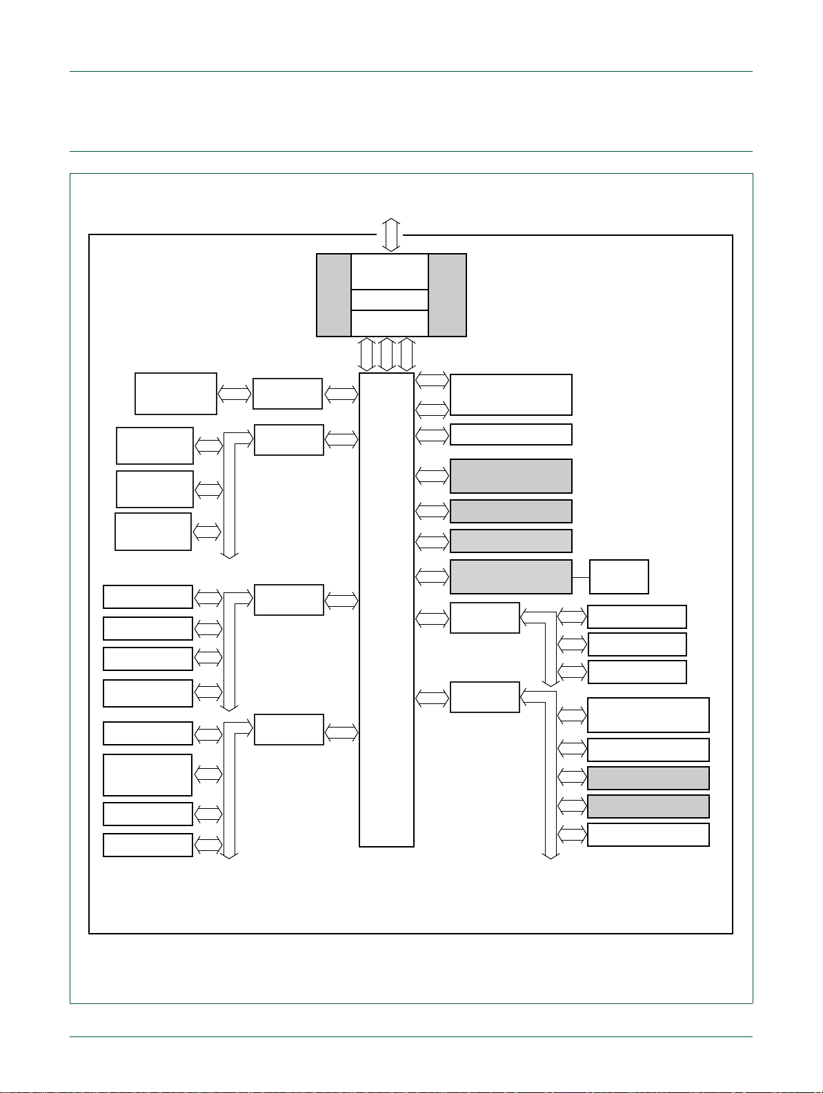
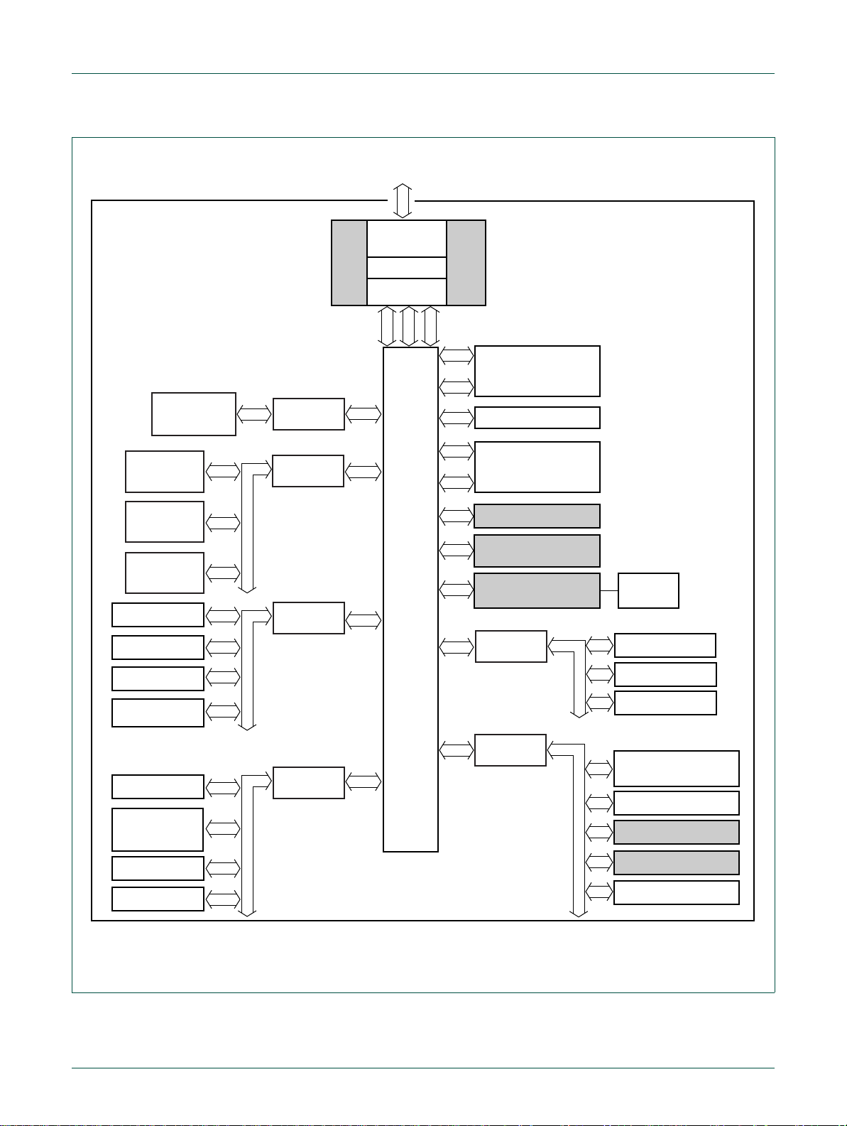
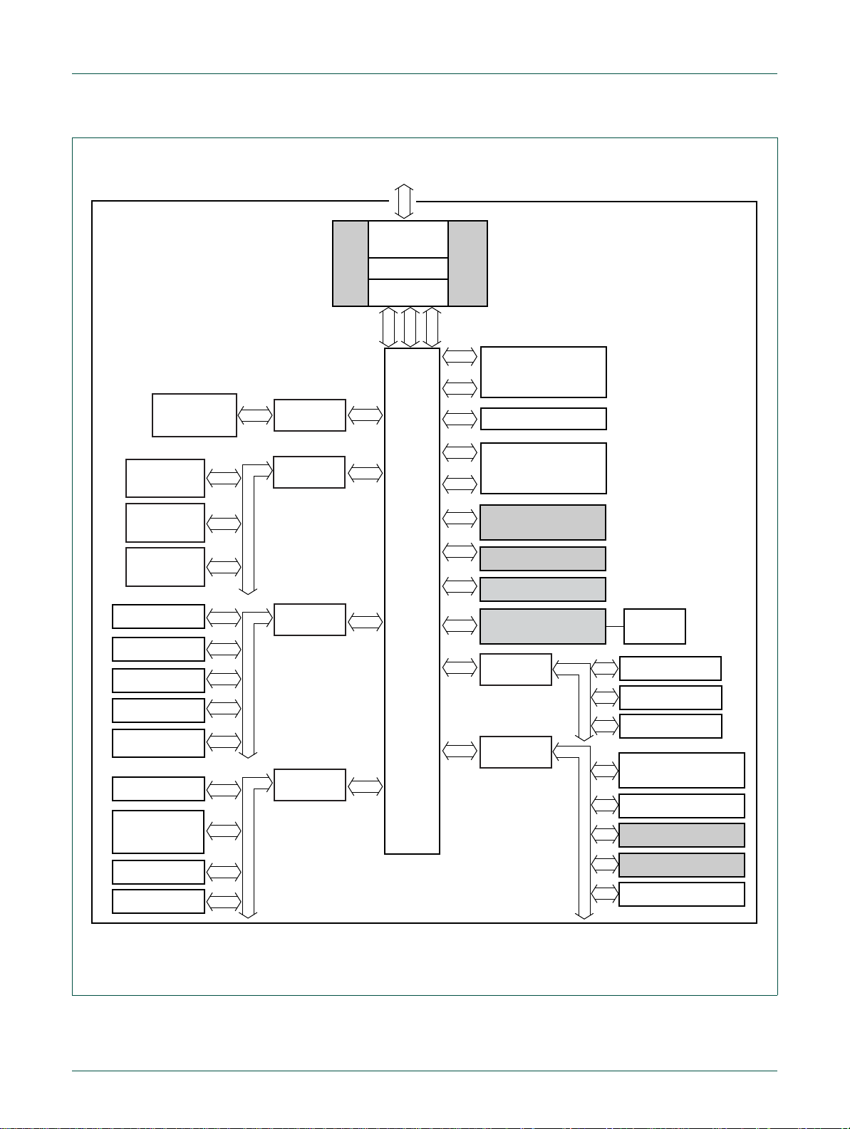
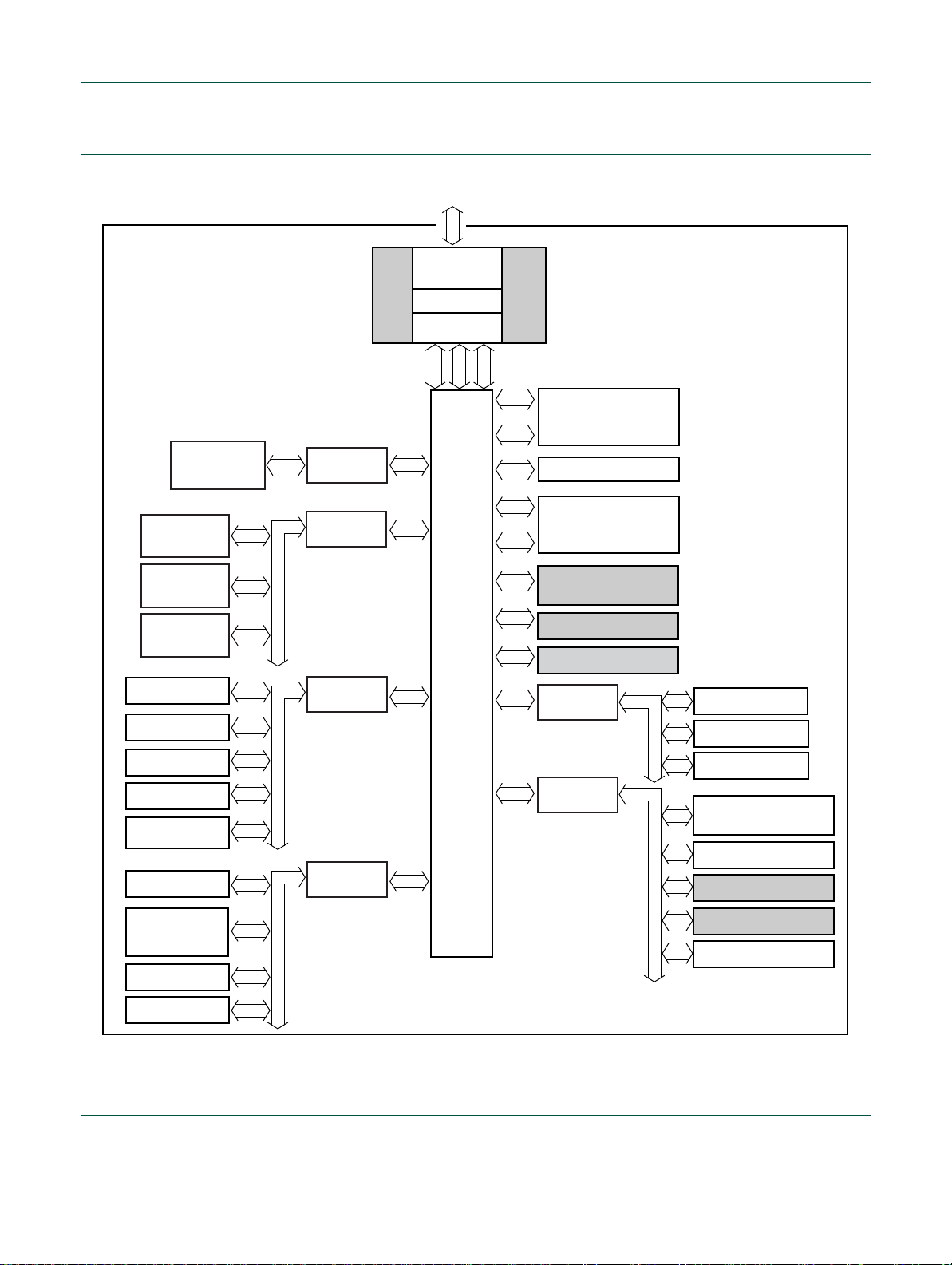
5. Block diagram
DRAFT
D
D
RAFT DRAFT DRAFT DRAFT DRAFT D
RAFT DRA
D
RAFT
UM10316
Chapter 1: LPC29xx Introductory information
F
T DRAFT DRAFT DRAFT DRA
DR
AFT
DRAFT
DRA
DR
AFT
DRAFT
DR
F
T DRAF
Fig 1. LPC2917/19/01 block diagram
Grey-shaded blocks represent peripherals with connections to the GPDMA.
UM10316_1 © NXP B.V. 2009. All rights reserved.
User manual Rev. 01.01 — 14 July 2009 8 of 568
Page 9
NXP Semiconductors
EMBEDDED FLASH
512/256/128 kB
002aae224
ARM968E-S
DTCM
16 kB
ITCM
16 kB
TEST/DEBUG
INTERFACE
slave
master
1 master
2 slaves
master
GPDMA CONTROLLER
GPDMA REGISTERS
16 kB
EEPROM
EMBEDDED SRAM 16 kB
(LPC2925 only)
SYSTEM CONTROL
TIMER0/1 MTMR
CAN0/1
GLOBAL
ACCEPTANCE
FILTER
PWM0/1/2/3
3.3 V ADC1/2
EVENT ROUTER
EMBEDDED SRAM 16 kB
GENERAL PURPOSE I/O
PORTS 0/1/5
TIMER 0/1/2/3
SPI0/1/2
RS-485 UART0/1
WDT
AHB TO APB
BRIDGE
AHB TO DTL
BRIDGE
VECTORED
INTERRUPT
CONTROLLER
master
slave
USB DEVICE
CONTROLLER
slave
slave
slave
slave
slave
slave
slave
slave
slave
AHB TO DTL
BRIDGE
AHB TO APB
BRIDGE
QUADRATURE
ENCODER
CHIP FEATURE ID
AHB TO APB
BRIDGE
I2C0/1
UART/LIN0/1
AHB TO APB
BRIDGE
AHB
MULTILAYER
MATRIX
LPC2921/2923/2925
JTAG
interface
8 kB SRAM
general subsystem
power, clock, and
reset subsystem
MSC subsystem
networking subsystem
peripheral subsystem
CLOCK
GENERATION
UNIT
POWER
MANAGEMENT
UNIT
RESET
GENERATION
UNIT
DRAFT
D
D
RAFT DRAFT DRAFT DRAFT DRAFT D
RAFT DRA
D
RAFT
UM10316
Chapter 1: LPC29xx Introductory information
F
T DRAFT DRAFT DRAFT DRA
DR
AFT
DRAFT
DRA
DR
AFT
DRAFT
DR
F
T DRAF
Fig 2. LPC2921/23/25 block diagram
UM10316_1 © NXP B.V. 2009. All rights reserved.
User manual Rev. 01.01 — 14 July 2009 9 of 568
Grey-shaded blocks represent peripherals with connections to the GPDMA.
Page 10
NXP Semiconductors
002aae143
ARM968E-S
DTCM
32 kB
ITCM
32 kB
TEST/DEBUG
INTERFACE
slave
master
1 master
2 slaves
master
EXTERNAL STATIC
MEMORY CONTROLLER
GPDMA CONTROLLER
GPDMA REGISTERS
EMBEDDED FLASH
512/768 kB
16 kB
EEPROM
EMBEDDED SRAM 32 kB
SYSTEM CONTROL
TIMER0/1 MTMR
CAN0/1
GLOBAL
ACCEPTANCE
FILTER
UART/LIN0/1
PWM0/1/2/3
3.3 V ADC1/2
EVENT ROUTER
EMBEDDED SRAM 16 kB
GENERAL PURPOSE I/O
PORTS 0/1/2/3/5
TIMER 0/1/2/3
SPI0/1/2
RS485 UART0/1
WDT
AHB TO APB
BRIDGE
AHB TO DTL
BRIDGE
VECTORED
INTERRUPT
CONTROLLER
master
slave
USB OTG/DEVICE
CONTROLLER
slave
slave
slave
slave
slave
slave
slave
slave
slave
slave
AHB TO DTL
BRIDGE
AHB TO APB
BRIDGE
5 V ADC0
QUADRATURE
ENCODER
CHIP FEATURE ID
AHB TO APB
BRIDGE
I2C0/1
AHB TO APB
BRIDGE
CLOCK
GENERATION
UNIT
POWER
MANAGEMENT
UNIT
RESET
GENERATION
UNIT
AHB
MULTILAYER
MATRIX
LPC2927/2929
JTAG
interface
8 kB SRAM
general subsystem
power. clock, and
reset subsystem
MSC subsystem
networking subsystem
peripheral subsystem
DRAFT
D
D
RAFT DRAFT DRAFT DRAFT DRAFT D
RAFT DRA
D
RAFT
UM10316
Chapter 1: LPC29xx Introductory information
F
T DRAFT DRAFT DRAFT DRA
DR
AFT
DRAFT
DRA
DR
AFT
DRAFT
DR
F
T DRAF
Fig 3. LPC2927/29 block diagram
UM10316_1 © NXP B.V. 2009. All rights reserved.
User manual Rev. 01.01 — 14 July 2009 10 of 568
Grey-shaded blocks represent peripherals with connections to the GPDMA.
Page 11
NXP Semiconductors
002aae257
ARM968E-S
DTCM
32 kB
ITCM
32 kB
TEST/DEBUG
INTERFACE
slave
master
1 master
2 slaves
master
EXTERNAL STATIC
MEMORY CONTROLLER
GPDMA CONTROLLER
GPDMA REGISTERS
EMBEDDED SRAM 32 kB
SYSTEM CONTROL
TIMER0/1 MTMR
CAN0/1
GLOBAL
ACCEPTANCE
FILTER
UART/LIN0/1
PWM0/1/2/3
3.3 V ADC1/2
EVENT ROUTER
EMBEDDED SRAM 16 kB
GENERAL PURPOSE I/O
PORTS 0/1/2/3/4/5
TIMER 0/1/2/3
SPI0/1/2
RS485 UART0/1
WDT
AHB TO APB
BRIDGE
AHB TO DTL
BRIDGE
VECTORED
INTERRUPT
CONTROLLER
master
slave
USB HOST/OTG/DEVICE
CONTROLLER
slave
slave
slave
slave
slave
slave
slave
slave
slave
AHB TO DTL
BRIDGE
AHB TO APB
BRIDGE
5 V ADC0
QUADRATURE
ENCODER
CHIP FEATURE ID
AHB TO APB
BRIDGE
I2C0/1
AHB TO APB
BRIDGE
CLOCK
GENERATION
UNIT
POWER
MANAGEMENT
UNIT
RESET
GENERATION
UNIT
AHB
MULTILAYER
MATRIX
LPC2930
JTAG
interface
8 kB SRAM
general subsystem
power. clock, and
reset subsystem
MSC subsystem
networking subsystem
peripheral subsystem
DRAFT
D
D
RAFT DRAFT DRAFT DRAFT DRAFT D
RAFT DRA
D
RAFT
UM10316
Chapter 1: LPC29xx Introductory information
F
T DRAFT DRAFT DRAFT DRA
DR
AFT
DRAFT
DRA
DR
AFT
DRAFT
DR
F
T DRAF
Grey-shaded blocks represent peripherals with connections to the GPDMA.
Fig 4. LPC2930 block diagram
UM10316_1 © NXP B.V. 2009. All rights reserved.
User manual Rev. 01.01 — 14 July 2009 11 of 568
Page 12

NXP Semiconductors
002aae254
ARM968E-S
DTCM
32 kB
ITCM
32 kB
TEST/DEBUG
INTERFACE
slave
master
1 master
2 slaves
master
EXTERNAL STATIC
MEMORY CONTROLLER
GPDMA CONTROLLER
GPDMA REGISTERS
EMBEDDED FLASH
768 kB
16 kB
EEPROM
EMBEDDED SRAM 32 kB
SYSTEM CONTROL
TIMER0/1 MTMR
CAN0/1
GLOBAL
ACCEPTANCE
FILTER
UART/LIN0/1
PWM0/1/2/3
3.3 V ADC1/2
EVENT ROUTER
EMBEDDED SRAM 16 kB
GENERAL PURPOSE I/O
PORTS 0/1/2/3/4/5
TIMER 0/1/2/3
SPI0/1/2
RS485 UART0/1
WDT
AHB TO APB
BRIDGE
AHB TO DTL
BRIDGE
VECTORED
INTERRUPT
CONTROLLER
master
slave
USB HOST/OTG/DEVICE
CONTROLLER
slave
slave
slave
slave
slave
slave
slave
slave
slave
slave
AHB TO DTL
BRIDGE
AHB TO APB
BRIDGE
5 V ADC0
QUADRATURE
ENCODER
CHIP FEATURE ID
AHB TO APB
BRIDGE
I2C0/1
AHB TO APB
BRIDGE
CLOCK
GENERATION
UNIT
POWER
MANAGEMENT
UNIT
RESET
GENERATION
UNIT
AHB
MULTILAYER
MATRIX
LPC2939
JTAG
interface
8 kB SRAM
general subsystem
power. clock, and
reset subsystem
MSC subsystem
networking subsystem
peripheral subsystem
DRAFT
D
D
RAFT DRAFT DRAFT DRAFT DRAFT D
RAFT DRA
D
RAFT
UM10316
Chapter 1: LPC29xx Introductory information
F
T DRAFT DRAFT DRAFT DRA
DR
AFT
DRAFT
DRA
DR
AFT
DRAFT
DR
F
T DRAF
Fig 5. LPC2939 block diagram
UM10316_1 © NXP B.V. 2009. All rights reserved.
User manual Rev. 01.01 — 14 July 2009 12 of 568
Grey-shaded blocks represent peripherals with connections to the GPDMA.
Page 13

NXP Semiconductors
6. Functional blocks
This chapter gives an overview of the functional blocks, clock domains, and power modes.
See Table 1–2
The functional blocks are explained in detail in the following chapters. Several blocks are
gathered into subsystems and one or more of these blocks and/or subsystems are put into
a clock domain. Each of these clock domains can be configured individually for power
management (i.e. clock on or off and whether the clock respond s to sleep and wake-up
events).
Table 5. Functional blocks and clock domains
Short Description Comment
Clock domain AHB
ARM ARM9TDMI-S 32-bit RISC processor
SMC Static Memory Controller For external (static) memory banks
SRAM Internal Static Memory -
Clock domain Flash
Flash - Internal Flash Memory
FMC Flash Memory Controller Controller for the internal flash memory
Clock domain USB
USB USB OTG controller -
Clock domain DMA controller
GPDMA General Purpose DMA
Clock domain VIC
VIC Vectored Interrupt Controller Prioritized/vectored interrupt handling
Clock domain general subsystem
CFID Digital Chip ID Identifies the device and its possibilities
ER Event Router Routes wake-up events and external
SCU System Control Unit Configures memory map and I/O
Clock domain peripheral subsystem
GPIO General-Purpose
TMR Timer Provides match output and capture
UART Universal Asynchronous
WDT Watchdog Timer to guard (software) execution
SPI Serial Peripheral Interfac e Supports various industry-standard SPI
Clock domain modulation and sampling-control subsystem
DRAFT
D
D
RAFT DRAFT DRAFT DRAFT DRAFT D
RAFT DRA
D
RAFT
UM10316
DRAFT
Chapter 1: LPC29xx Introductory information
F
T DRAFT DRAFT DRAFT DRA
for availability of peripherals and blocks for specific LPC29xx parts.
controller
interrupts (to CGU/VIC)
functions
Directly controls I/O pins
Input/Output
inputs
Standard 550 serial port
Receiver/Transmitter
protocols
DR
AFT
DRA
DR
AFT
DRAFT
DR
F
T DRAF
ADC Analog-to-Digital Converter 10-bit Analog-to-Digital Converter
PWM Pulse-Width Modulator Synchronized Pulse-Width Modulator
UM10316_1 © NXP B.V. 2009. All rights reserved.
User manual Rev. 01.01 — 14 July 2009 13 of 568
Page 14

NXP Semiconductors
Table 5. Functional blocks and clock domains
Short Description Comment
TMR Timer Dedicated Sampling and Control Timer
QEI Quadrature encoder
Clock domain networking subsystem
CAN Gateway Includes acceptance filter
LIN Master controller LIN master controller
I2C I2C-bus
Clock domain power control subsystem
CGU0 Clock Generation Unit Controls clock sources and clock
CGU1 clock generation unit USB clocks and clock out
RGU reset generation unit PMU power management unit -
interface
DRAFT
Chapter 1: LPC29xx Introductory information
…continued
-
domains
D
RAFT DRAFT DRAFT DRAFT DRAFT D
D
RAFT DRA
D
RAFT
UM10316
F
T DRAFT DRAFT DRAFT DRA
DR
AFT
DRAFT
DRA
DR
AFT
DRAFT
DR
F
T DRAF
7. Architectural overview
The LPC29xx consists of:
• An ARM968E-S processor with real-time emulation support
• An AMBA multi-layer Advanced High-performance Bus (AHB) for interfacing to the
on-chip memory controllers
• Two DTL buses (an universal NXP interface) for interfacing to the interrupt controller
and the Power, Clock and Reset Control cluster (also called subsystem).
• Three ARM Peripheral Buses (APB - a compatible superset of ARM's AMBA
advanced peripheral bus) for connection to on-chip peripherals clustered in
subsystems.
• One ARM Peripheral Bus for event router and system control.
The LPC29xx configures the ARM968E-S processor in little-endian byte order. All
peripherals run at their own clock frequency to optimize the total system power
consumption. The AHB2APB bridge used in the subsystems contains a write-ahead buffer
one transaction deep. This implies that when the ARM968E-S issues a buff ered write
action to a register located on the APB side of the bridge, it continues even though the
actual write may not yet have taken place. Completion of a second write to the same
subsystem will not be executed until the first write is finished.
8. ARM968E-S processor
The ARM968E-S is a general purpose 32-bit RISC processor, which offers high
performance and very low power consumption. The ARM architecture is based on
Reduced Instruction Set Computer (RISC) principles, and the instruction set and related
decode mechanism are much simpler than those of microprogrammed Complex
Instruction Set Computers (CISC). This simplicity results in a high instruction throughput
and impressive real-time interrupt respon se fro m a sm all and co st- effective con tr olle r
core.
UM10316_1 © NXP B.V. 2009. All rights reserved.
User manual Rev. 01.01 — 14 July 2009 14 of 568
Page 15

NXP Semiconductors
Amongst the most compelling features of the ARM968E-S are:
• Separate directly connected instruction and data Tightly Coupled Memory (TCM)
• Write buffers for the AHB and TCM buses
• Enhanced 16 × 32 multiplier capable of single-cycle MAC operations and 16-bit fixed-
Pipeline techniques are employed so that all pa rts of the p rocessing and memory systems
can operate continuously. The ARM968E-S is based on the ARMv5TE five-stage pipeline
architecture. Typica lly, in a three-stage pipeline architecture, while one instruction is being
executed its successor is being decoded and a third instruction is being fetched from
memory. In the five-stage pipeline additional stages are added for memory access and
write-back cycles.
The ARM968E-S processor also employs a unique architectural strategy known as
THUMB, which makes it ideally suited to high-volume applications with memory
restrictions or to applications where code density is an issue.
DRAFT
Chapter 1: LPC29xx Introductory information
interfaces
point DSP instructions to accelerate signal-processing algorithms and applications.
D
RAFT DRAFT DRAFT DRAFT DRAFT D
D
RAFT DRA
D
RAFT
UM10316
F
T DRAFT DRAFT DRAFT DRA
DR
AFT
DRAFT
DRAFT
DRA
F
DR
AFT
DR
T DRAF
The key idea behind THUMB is that of a super-reduced instruction set. Essentially, the
ARM968E-S processor has two instruction sets:
• Standard 32-bit ARMv5TE set
• 16-bit THUMB set
The THUMB set's 16-bit instruction length allows it to approach twice the density of
standard ARM code while retaining most of the ARM's performance advantage over a
traditional 16-bit controller using 16-bit registers. This is possible because THUMB code
operates on the same 32-bit register set as ARM code.
THUMB code can provide up to 65 % of the code size of ARM, and 160 % of the
performance of an equivalent ARM controller connected to a 16-bit memory system.
The ARM968E-S processor is described in detail in the ARM968E-S data sheet.
9. On-chip flash memory system
The LPC29xx includes up to 768 kB flash memory. This memory can be used for both
code and data storage. Flash memory can be programmed in- system via a serial port
(e.g., CAN).
10. On-chip static RAM
In addition to the two 16 kB or 32 kB TCMs, the LPC29xx includes two static RAM
memories: one of up to 32 kB and one of 16 kB. Both may be used for code and/or data
storage.
UM10316_1 © NXP B.V. 2009. All rights reserved.
User manual Rev. 01.01 — 14 July 2009 15 of 568
Page 16

UM10316
Chapter 2: LPC29xx memory mapping
Rev. 01.01 — 14 July 2009 User manual
1. How to read this chapter
The memory configuration varies for the different LPC29xx parts (see Table 2–6). In
addition to the memory blocks, peripheral register blocks in memory region 7 are available
only if the peripheral is implemented. See Table 2–7
peripheral registers are available on all LPC29xx parts.
Table 6. LPC29xx memory configurations
Part number Flash SRAM TCM (I/D) SMC
LPC2917/01 512 kB 32 kB 16 kB yes 16/16 kB 8 banks, 16 MB each
LPC2919/01 768 kB 32 kB 16 kB yes 16/16 kB 8 banks, 16 MB each
LPC2921 128 kB 16 kB - yes 16/16 kB LPC2923 256 kB 16 kB - yes 16/16 kB LPC2925 512 kB 16 kB 16 kB yes 16/16 kB LPC2927 512 kB 32 kB 16 kB yes 32/32 kB 8 banks, 16 MB each
LPC2929 768 kB 32 kB 16 kB yes 32/32 kB 8 banks, 16 MB each
LPC2930 - 32 kB 16 kB yes 32/32 kB 8 banks, 16 MB each
LPC2939 768 kB 32 kB 16 kB yes 32/32 kB 8 banks, 16 MB each
SRAM @
0x8000 0000
SRAM @
0x8000 8000
DRAFT
D
D
RAFT DRAFT DRAFT DRAFT DRAFT D
RAFT DRA
D
RAFT
DRAFT
F
T DRAFT DRAFT DRAFT DRA
for part specific registers. All other
ETB
(8 kB)
DR
AFT
DRA
DR
AFT
DRAFT
DR
F
T DRAF
Table 7. LPC29xx configuration of peripheral registers
Part number peripheral
cluster #2
GPIO ADC0 ADC1 ADC2 USB
LPC291719/01 GPIO0/1/2/3 no yes yes no
LPC2919/01 GPIO0/1/2/3 no yes yes no
LPC2921 GPIO0/1/5 no yes yes yes
LPC2923 GPIO0/1/5 no yes yes yes
LPC2925 GPIO0/1/5 no yes yes yes
LPC2927 GPIO0/1/2/3/5 yes yes yes yes
LPC2929 GPIO0/1/2/3/5 yes yes yes yes
LPC2930 GPIO0/1/2/3/4/5 yes yes yes yes
LPC2939 GPIO0/1/2/3/4/5 yes yes yes yes
2. Memory-map view of the AHB
The LPC29xx uses an AHB multilayer bus with the CPU and the GPDMA as the bus
masters. The AHB slaves are connected to the AHB-lite multilayer bus.The ARM968E-S
CPU has access to all AHB slaves and hence to all address regions.
peripheral cluster #6 AHB
peripherals
UM10316_1 © NXP B.V. 2009. All rights reserved.
User manual Rev. 01.01 — 14 July 2009 16 of 568
Page 17

NXP Semiconductors
3. Memory-map regions
The ARM9 processor has a 4 GB of address space. The LPC29xx has divided this
memory space into eight regions of 512 MB each. Each region is used for a dedicated
purpose.
An exception to this is region 0; several of the other regions (or a part of it) can be
shadowed in the memory map at this region. This shadowing can be controlled by
software via the programmable re-mapping registers (see Table 6–64
Table 8. LPC29xx memory regions
Memory region # Address Description
0 0x0000 0000 TCM area and shadow area
1 0x2000 0000 embedded flash area
2 0x4000 0000 external static memory area
3 0x6000 0000 external static memory controller area
4 0x8000 0000 internal SRAM area
5 0xA000 0000 not used
6 0xC000 0000 not used
7 0xE000 0000 bus-peripherals area
DRAFT
D
D
RAFT DRAFT DRAFT DRAFT DRAFT D
RAFT DRA
D
RAFT
UM10316
Chapter 2: LPC29xx memory mapping
F
T DRAFT DRAFT DRAFT DRA
DR
AFT
DRAFT
DRA
).
DR
AFT
DRAFT
DR
F
T DRAF
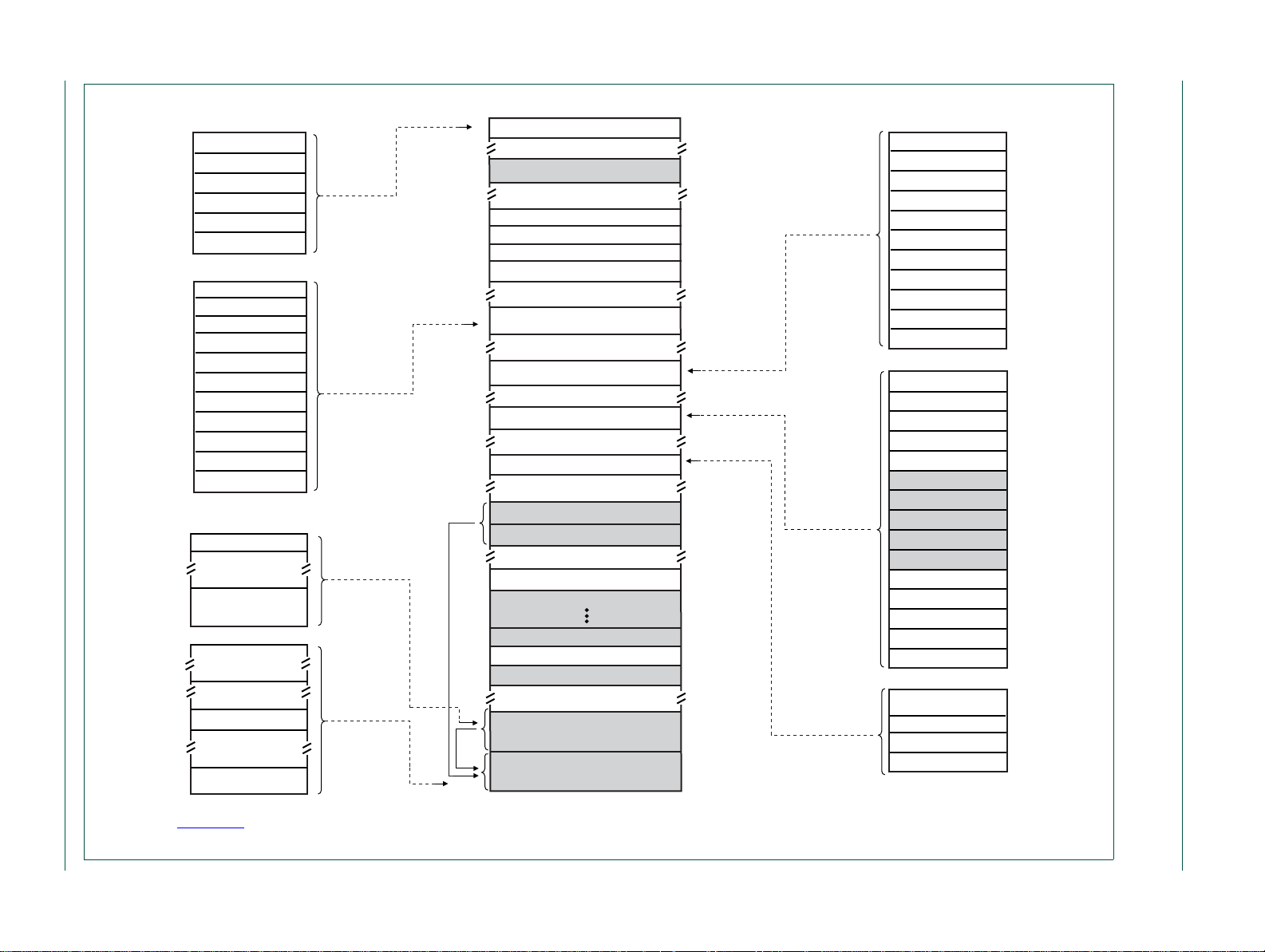
Figure 2–6 gives a graphical overview of the LPC29xx memory map.
UM10316_1 © NXP B.V. 2009. All rights reserved.
User manual Rev. 01.01 — 14 July 2009 17 of 568
Page 18
User manual Rev. 01.01 — 14 July 2009 18 of 568
16 MB ext. static memory bank 0
(1)
16 MB ext. static memory bank 1
(1)
ext. static memory banks 7 to 2
(1)
reserved
DMA interface to TCM
PCR/VIC control
0x0000 0000
0 GB
1 GB
4 GB
2 GB
0x4000 0000
0x4100 0000
0x4300 0000
0x4200 0000
0x2000 0000
0x6000 0000
0x6000 4000
0x8000 0000
0x8000 8000
0x8000 C000
0xE000 0000
0xE002 0000
0xE004 0000
0xE006 0000
0xE008 0000
0xE00A 0000
0xE00C 0000
0xE00E 0000
0xE010 0000
0xE014 0000
0xE018 3000
0xF000 0000
0xF080 0000
0xFFFF 8000
0xFFFF FFFF
reserved
reserved
reserved
reserved
reserved
reserved
reserved
peripheral subsystem #0
peripheral subsystem #2
peripheral subsystem #4
peripheral subsystem #6
0xE018 2000
0xE018 0000
32 kB AHB SRAM
(1)
16 kB AHB SRAM
(1)
reserved
USB controller
(1)
DMA controller
8 kB ETB SRAM
ETB control
reserved
ITCM/DTCM
on-chip flash
(1)
0x2020 4000
0x0000 0000
0x0040 0000
0x0000 8000
0x0040 8000
0x0080 0000
0x2000 0000
32 kB
(1)
ITCM
32 kB
(1)
DTCM
reserved
reserved
no physical memory
peripherals #6
MSCSS
subsystem
ITCM/DTCM
memory
EMI/SMC
(1)
peripherals #2
peripheral
subsystem
0xE004 1000
0xE004 2000
0xE004 3000
0xE004 4000
0xE004 6000
0xE004 8000
0xE004 A000
0xE004 B000
0xE004 D000
0xE005 0000
0xE006 0000
0xE004 C000
0xE004 9000
0xE004 7000
0xE004 5000
0xE004 0000
SPI0
WDT
TIMER0
TIMER1
TIMER2
TIMER3
UART0
UART1
SPI1
SPI2
GPIO0
GPIO1
GPIO2
(1)
GPIO3 to GPIO5
(1)
peripherals #0
general
subsystem
0xE000 1000
0xE000 2000
0xE000 2000
0xE002 0000
0xE000 0000
CFID
SCU
event router
peripherals #4
networking
subsystem
0xE008 1000
0xE008 0000
CAN0
CAN1
0xE008 2000
0xE008 3000
0xE008 4000
0xE008 7000
0xE008 9000
0xE008 B000
0xE00A 0000
0xE008 A000
0xE008 8000
0xE008 6000
I2C0
I2C1
reserved
CAN ID LUT
CAN common regs
LIN0
LIN1
CAN AF regs
0xE00C 0000
0xE00C 1000
0xE00C 2000
0xE00C 3000
0xE00C 4000
0xE00C 5000
0xE00C 6000
0xE00C 7000
0xE00C 8000
0xE00C 9000
0xE00C A000
0xE00E 0000
ADC0 (5V)
(1)
ADC1
ADC2
PWM0
PWM1
PWM3
quadrature encoder
PWM2
MSCSS timer0
MSCSS timer1
PCR/VIC
subsystem
0xFFFF 8000
0xFFFF 9000
0xFFFF A000
0xFFFF B000
0xFFFF C000
0xFFFF F000
0xFFFF FFFF
PMU
CGU1
reserved
reserved
reserved
reserved
reserved
VIC
CGU0
RGU
512 MB shadow area
remappable to
shadow area
LPC29xx
768 kB
(1)
on-chip
flash
flash controller
0x2000 0000
reserved
0x200C 0000
0x2020 0000
0x2020 4000
flash
memory
xxxxxxxxxxxxxxxxxxxxx xxxxxxxxxxxxxxxxxxxxxxxxxx xxxxxxx x x x xxxxxxxxxxxxxxxxxxxxxxxxxxxxxx xxxxxxxxxxxxxxxxxxx xx xx xxxxx
xxxxxxxxxxxxxxxxxxxxxxxxxxx xxxxxxxxxxxxxxxxxxx xxxxxx xxxxxxxxxxxxxxxxxxxxxxxxxxxxxxxxxxx xxxxxxxxxxxx x x
xxxxxxxxxxxxxxxxxxxxx xxxxxxxxxxxxxxxxxxxxxxxxxxxxxx xxxxx xxxxxxxxxxxxxxxxxxxxxxxxxxxxxxxxxxxxxxxxxxxxxxxxxx xxxxxxxx
UM10316_1 © NXP B.V. 2009. All rights reserved.
xxxxxxxxxxxxxxxxxxxxxxxxx xxxxxxxxxxxxxxxxxxxx xxx
NXP Semiconductors
Fig 6. LPC29xx system memory map: graphical overview
(1) See Section 2–1 for part-specific implementation. Gray-shaded memory regions are accessible by the GPDMA controller.
Chapter 2: LPC29xx memory mapping
DRAFT
D
RAFT DRA
D
RAFT DRAFT DRAFT DRAFT DRAFT D
UM10316
F
T DRAFT DRAFT DRAFT DRA
DRA
F
T DRAF
DR
D
RAFT
DRAFT
DR
AFT
DRAFT
DR
AFT
Page 19
NXP Semiconductors
Region #0:TCM area
0x0000_0000 - 0x1FFF_FFFF
(Offset Address
0x0000 0000
0x1FFF FFFF
0x0000 4000/0
0x0040 0000
I-TCM region aliasses
I-TCM (16/32 kByte)
0x0080 0000
D-TCM region aliasses
D-TCM (16 kByte)
region #0 no physical memory
0x0040 4000/0
3.1 Region 0: TCM/shadow area
The ARM968E-S processor has its exception vectors located at address logic 0. Since
flash is the only non-volatile memory available in the LPC29xx, the exception vectors in
the flash must be located at address logic 0 at reset (AHB_RST).
DRAFT
D
D
RAFT DRAFT DRAFT DRAFT DRAFT D
RAFT DRA
D
RAFT
UM10316
Chapter 2: LPC29xx memory mapping
F
T DRAFT DRAFT DRAFT DRA
DR
AFT
DRAFT
DRA
DR
AFT
DRAFT
DR
F
T DRAF
UM10316_1 © NXP B.V. 2009. All rights reserved.
User manual Rev. 01.01 — 14 July 2009 19 of 568
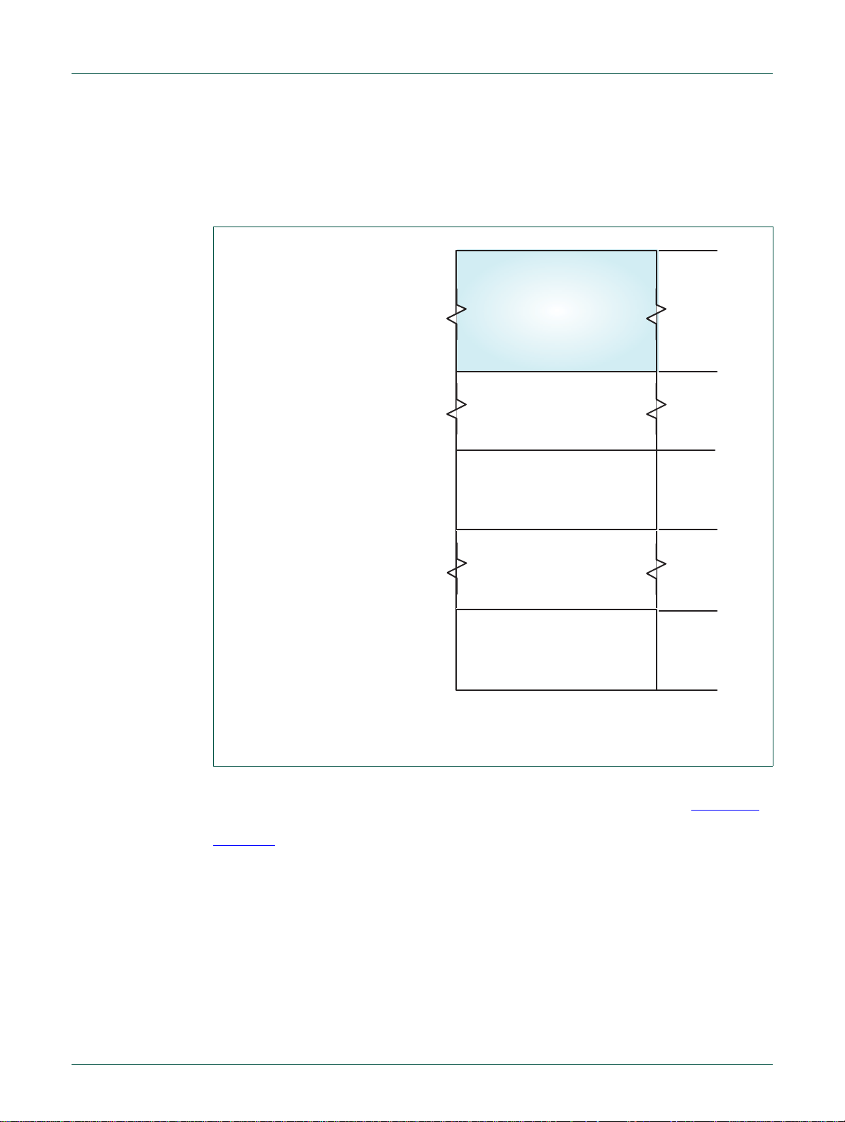
Fig 7. Region 0 memory map
After booting a choice must be made for region 0. When enable d, the Tightly Coupled
Memories (TCMs) occupy fixed address locations in region 0 as indicated in Figure 2–6
Information on how to enable the TCMs can be found in the ARM documentation, see
Ref. 31–2
To enable memory re-mapping, the LPC29xx AHB system memory map provides a
shadow area (region 0) starting at address log ic 0 . This is a vir tual memo ry re gio n, i.e. no
actual memory is present at the shadow area addresses. A selectable region of the AHB
.
.
system memory map is, apart from its own specific region, also accessible via this shadow
area region.
Page 20

NXP Semiconductors
+ 0x00000000
+ 0x1FFFFFFF
+ 0x00200000
FLASH IF1
Configuration Area (4 Kbyte)
+ 0x00200FFF
Embedded FLASH
memory area
512 Kbyte -
768 Kbyte
+ 0x0007FFFF - 0x000BFFF
After reset, the region 1 embedded flash area is always available at the shadow area.
After booting, any other region of the AHB system memory map (e.g. internal SRAM) can
be re-mapped to region 0 by means of the shadow memory mapping register. For more
details about the shadow area see Table 6–64
3.2 Region 1: embedded flash area
Figure 2–8 gives a graphical overview of the embedded flash memory map.
DRAFT
D
D
RAFT DRAFT DRAFT DRAFT DRAFT D
RAFT DRA
D
RAFT
UM10316
DR
DRAFT
Chapter 2: LPC29xx memory mapping
F
T DRAFT DRAFT DRAFT DRA
.
AFT
DRA
DR
AFT
DRAFT
DR
F
T DRAF
Fig 8. Region 1 embedded flash memory
Region 1 is reserved for the embedded flash. A data area of 2 Mbyte (to be prepared for a
larger flash-memory instance) and a configuration area of 4 kB are reserved for each
embedded flash instance. Although the LPC29xx contains only one embedded flash
instance, the memory aperture per instance is defined at 4 Mbyte.
3.3 Region 2: external static memory area
Region 2 is reserved for the external static memory. The LPC29xx provides I/O pins for
eight bank-select signals and 24 address lines. This implies that eight memory banks of
UM10316_1 © NXP B.V. 2009. All rights reserved.
User manual Rev. 01.01 — 14 July 2009 20 of 568
16 Mbytes each can be addressed externally.
3.4 Region 3: external static memory controller area
The external Static-Memory Controller configuration area is located at region 3
3.5 Region 4: internal SRAM area
Figure 2–6 gives a graphical overview of the internal SRAM memory map.
Page 21

NXP Semiconductors
Region 4 is reserved for internal SRAM. The LPC29xx has two internal SRAM instances.
Instance #0 is 32 kB, instance #1 is 16 kB. See Section 7–1
3.6 Regions 5 and 6
Regions 5 and 6 are not used.
3.7 Region 7: bus-peripherals area
Figure 2–6 gives a graphical overview of the bus-peripherals area memory map.
Region 7 is reserved for all stand-alone memory-mapped bus peripherals.
The lower part of region 7 is again divided into APB clusters, also referred to as
subsystems in this User Manual. A APB cluster is typically used as the address space for
a set of APB peripherals connected to a single AHB2APB bridge, the slave on the AHB
system bus. The clusters are aligned on 256 kB boundaries. In the LPC29xx four APB
clusters are in use: General SubSystem (GeSS), Peripheral SubSystem (PeSS) ,
Networking SubSystem (IVNSS), and the Modulation and Sampling SubSystem
(MSCSS). The APB peripherals are aligned on 4 kB boundaries inside the APB clusters.
D
RAFT
UM10316
F
T DRAFT DRAFT DRAFT DRA
D
RAFT DRA
.
D
RAFT DRAFT DRAFT DRAFT DRAFT D
DRAFT
Chapter 2: LPC29xx memory mapping
DR
AFT
DRAFT
DRA
DR
AFT
DRAFT
DR
F
T DRAF
The upper part of region 7 is used as the memory area where memory-mapped register
interfaces of stand-alone AHB peripherals and a DTL cluster reside. Each of these is a
slave on the AHB system bus. In the LPC29xx two such slaves are present: the Power,
Clock and Reset subsystem (PCRSS) and the Vectored Interrupt Controller (VIC). The
PCRSS is a DTL cluster in which the CGU, PMU and RGU are connected to the AHB
system bus via an AHB2DTL adapter. The VIC is a DTL target connected to the AHB
system bus via its own AHB2DTL adapter.
4. Memory-map operating concepts
The basic concept in the LPC29xx is that each memory area has a ‘natural’ location in the
memory map. This is the address range for which code residing in that area is written.
Each memory space remains permanently fixed in the same location, elim inating the need
to have portions of the code designed to run in different address ranges.
Because of the location of the exception-handler vectors on the ARM9 processor (at
addresses 0000 0000h through 0000 001Ch: see Table 2–9
embedded flash is mapped at address 0000 0000h to allow initial code to be executed
and to perform the required initialization, which starts executing at 0000 0000h.
The LPC29xx generates the appropriate bus-cycle abort exception if an access is
attempted for an address that is in a reserved or unused address region or unassigned
peripheral spaces. For these areas both attempted data accesses and instruction fetches
generate an exception. Note that write-access addresses should be word-aligned in ARM
code or half-word aligned in Thumb code. Byte-aligned writes are performed as word or
half-word aligned writes without error signalling.
) By default, after reset, the
Within the address space of an existing peripheral a dat a-abort exception is not gen erated
in response to an access to an undefined address. Address decoding within each
peripheral is limited to that needed to distinguish defined registers within the peripheral
itself. Details of address aliasing within a peripheral sp ace are not defined in the LPC29xx
documentation and are not a supported feature.
UM10316_1 © NXP B.V. 2009. All rights reserved.
User manual Rev. 01.01 — 14 July 2009 21 of 568
Page 22

NXP Semiconductors
Note that the ARM stores the pre-fetch abort flag along with the associated instruction
(which will be meaningless) in the pipeline and processes the abort only if an attempt is
made to execute the instruction fetched from the illegal address. This prevents the
accidental aborts that could be caused by pre-fetches occurring when code is executed
very near to a memory boundary.
DRAFT
D
D
RAFT DRAFT DRAFT DRAFT DRAFT D
RAFT DRA
D
RAFT
UM10316
Chapter 2: LPC29xx memory mapping
F
T DRAFT DRAFT DRAFT DRA
DR
AFT
DRAFT
DRA
DR
AFT
DRAFT
DR
F
T DRAF
Table 2–10
Table 9. Interrupt vectors address table
Address Exception
0x0000 0000 Reset
0x0000 0004 Undefined instruction
0x0000 0008 Software interrupt
0x0000 000C Pre-fetch abort (instruction-fetch memory fault)
0x0000 0010 Data abort (data-access memory fault)
0x0000 0014 reserved
0x0000 0018 IRQ
0x0000 001C FIQ
Table 10. Peripherals base-address overview
Base address Base name AHB peripherals
Memory region 0 to region 6
0x0000 0000 TCM memory
0x2000 0000 Embedded flash memory
0x2020 0000 FMC RegBase Embedded-flash controller
0x4000 0000 External static memory
0x6000 0000 SMC RegBase External Static-Memory Controller
0x8000 0000 Internal SRAM memory
APB Cluster 0: general subsystem
0xE000 0000 CFID RegBase Chip/feature ID register
0xE000 1000 SCU RegBase System Control Unit
0xE000 2000 ER RegBase Event Router
APB Cluster 2: peripheral subsystem
0xE004 0000 WDT RegBase Watchdog Timer
0xE004 1000 TMR RegBase Timer 0
0xE004 2000 TMR RegBase Timer 1
0xE004 3000 TMR RegBase Timer 2
0xE004 4000 TMR RegBase Timer 3
0xE004 5000 UART RegBase UART 0
0xE004 6000 UART RegBase UART 1
0xE004 7000 SPI RegBase SPI 0
0xE004 8000 SPI RegBase SPI 1
0xE004 9000 SPI RegBase SPI 2
gives the base address overview of all peripherals:
configuration registers
configuration registers
UM10316_1 © NXP B.V. 2009. All rights reserved.
User manual Rev. 01.01 — 14 July 2009 22 of 568
Page 23

NXP Semiconductors
Table 10. Peripherals base-address overview
Base address Base name AHB peripherals
0xE004 A000 GPIO RegBase General-Purpose I/O 0
0xE004 B000 GPIO RegBase General-Purpose I/O 1
0xE004 C000 GPIO RegBase General-Purpose I/O 2
0xE004 D000 GPIO RegBase General-Purpose I/O 3
0xE004 E000 GPIO RegBase General-Purpose I/O 4
0xE004 F000 GPIO RegBase General-Purpose I/O 5
APB Cluster 4: networking subsystem
0xE008 0000 CANC RegBase CAN controller 0
0xE008 1000 CANC RegBase CAN controller 1
0xE008 2000 I2C RegBase I
0xE008 3000 I2C Regbase I
0xE008 6000 CANAFM RegBase CAN ID look-up table memory
0xE008 7000 CANAFR RegBase CAN acceptance filter registers
0xE008 8000 CANCS RegBase CAN central status registers
0xE008 9000 LIN RegBase LIN master controller 0
0xE008 A000 LIN RegBase LIN master controller 1
APB Cluster 6: modulation and sampling-control subsystem
0xE00C 0000 MTMR RegBase MSCSS timer 0
0xE00C 1000 MTMR RegBase MSCSS timer 1
0xE00C 2000 ADC RegBase ADC 0
0xE00C 3000 ADC RegBase ADC 1
0xE00C 4000 ADC RegBase ADC 2
0xE00C 5000 PWM RegBase PWM 0
0xE00C 6000 PWM RegBase PWM 1
0xE00C 7000 PWM RegBase PWM 2
0xE00C 8000 PWM RegBase PWM 3
0xE00C 9000 QEI RegBase Quadrature encoder interface
AHB peripherals: DMA controller, USB controller
E010 0000 USB RegBase USB controller registers
E014 0000 DMA RegBase GPDMA controller registers
Power, Clock and Reset control cluster
FFFF 8000 CGU RegBase Clock Generation Unit
FFFF 9000 RGU RegBase Reset Generation Unit
FFFF A000 PMU RegBase Power Management Unit
Vector interrupt controller
FFFF F000 VIC RegBase Vectored Interrupt Controller
DRAFT
D
D
RAFT DRAFT DRAFT DRAFT DRAFT D
RAFT DRA
D
RAFT
UM10316
DRAFT
Chapter 2: LPC29xx memory mapping
F
T DRAFT DRAFT DRAFT DRA
…continued
2
C0-bus interface
2
C1-bus interface
DR
AFT
DRA
DR
AFT
DRAFT
DR
F
T DRAF
UM10316_1 © NXP B.V. 2009. All rights reserved.
User manual Rev. 01.01 — 14 July 2009 23 of 568
Page 24

UM10316
Chapter 3: LPC29xx Clock Generation Unit (CGU)
Rev. 01.01 — 14 July 2009 User manual
1. How to read this chapter
This chapter describes the base clock generation for all LPC29xx parts. CGU0 is identical
for all parts. CGU1 is configuration dependent.
T able 11. LPC29xx base clock options
Part CGU0 base
clocks
LPC2917/19/01 see Table 3–12
LPC2921/23/25 see Table 3–12
LPC2927/29 see Table 3–12
LPC2939 see Table 3–12
LPC2930 see Table 3–12
DRAFT
D
D
RAFT DRAFT DRAFT DRAFT DRAFT D
D
RAFT
RAFT DRA
DR
AFT
DRAFT
DRA
F
T DRAFT DRAFT DRAFT DRA
CGU1 base clocks
BASE_OUT_CLK
BASE_OUT_CLK, BASE_USB_CLK
BASE_OUT_CLK, BASE_USB_CLK, BASE_USB_I2C_CLK
BASE_OUT_CLK, BASE_USB_CLK, BASE_USB_I2C_CLK
BASE_OUT_CLK, BASE_USB_CLK, BASE_USB_I2C_CLK
DR
AFT
DRAFT
DR
F
T DRAF
2. Introduction
The CGU0 is part of the Power Control, Clock, and Reset control (PCR) block and
provides the clocks for all subsystems. A second, dedicated CGU1 provides the clocks for
the USB block and a clock output. The CGU1 has two clock inputs to its PLL which are
internally connected to two base clocks in the CGU0.
Both CGUs are functionally identical and have their own PLL and fractional divider
registers.
UM10316_1 © NXP B.V. 2009. All rights reserved.
User manual Rev. 01.01 — 14 July 2009 24 of 568
Page 25
NXP Semiconductors
TIMER0/1 MTMR
PWM0/1/2/3
ADC0/1/2
QEI
modulation and sampling
control subsystem
BASE_MSCSS_CLK
branch
clocks
branch
clocks
BASE_ADC_CLK
BASE_ICLK0_CLK
BASE_ICLK1_CLK
CAN0/1
GLOBAL
ACCEPTANCE
FILTER
LIN0/1
I2C0/1
networking subsystem
BASE_IVNSS_CLK
branch
clocks
RESET/CLOCK
GENERATION &
POWER
MANAGEMENT
power control subsystem
BASE_PCR_CLK
branch
clock
GPIO0 to 5
TIMER 0/1/2/3
SPI0/1/2
UART0/1
WDT
BASE_SYS_CLK
CPU
AHB MULTILAYER MATRIX
VIC
GPDMA
USB REGISTERS
FLASH/SRAM/SMC
general subsytem
peripheral subsystem
AHB TO APB BRIDGES
SYSTEM CONTROL
EVENT ROUTER
CFID
branch
clocks
BASE_SAFE_CLK
BASE_UART_CLK
BASE_SPI_CLK
BASE_TMR_CLK
CGU0
CGU1
BASE_USB_CLK
BASE_USB_I2C_CLK
BASE_OUT_CLK
USB
CLOCK
OUT
DRAFT
D
D
RAFT DRAFT DRAFT DRAFT DRAFT D
RAFT DRA
D
RAFT
UM10316
Chapter 3: LPC29xx Clock Generation Unit (CGU)
F
T DRAFT DRAFT DRAFT DRA
DR
AFT
DRAFT
DRA
DR
AFT
DRAFT
DR
F
T DRAF
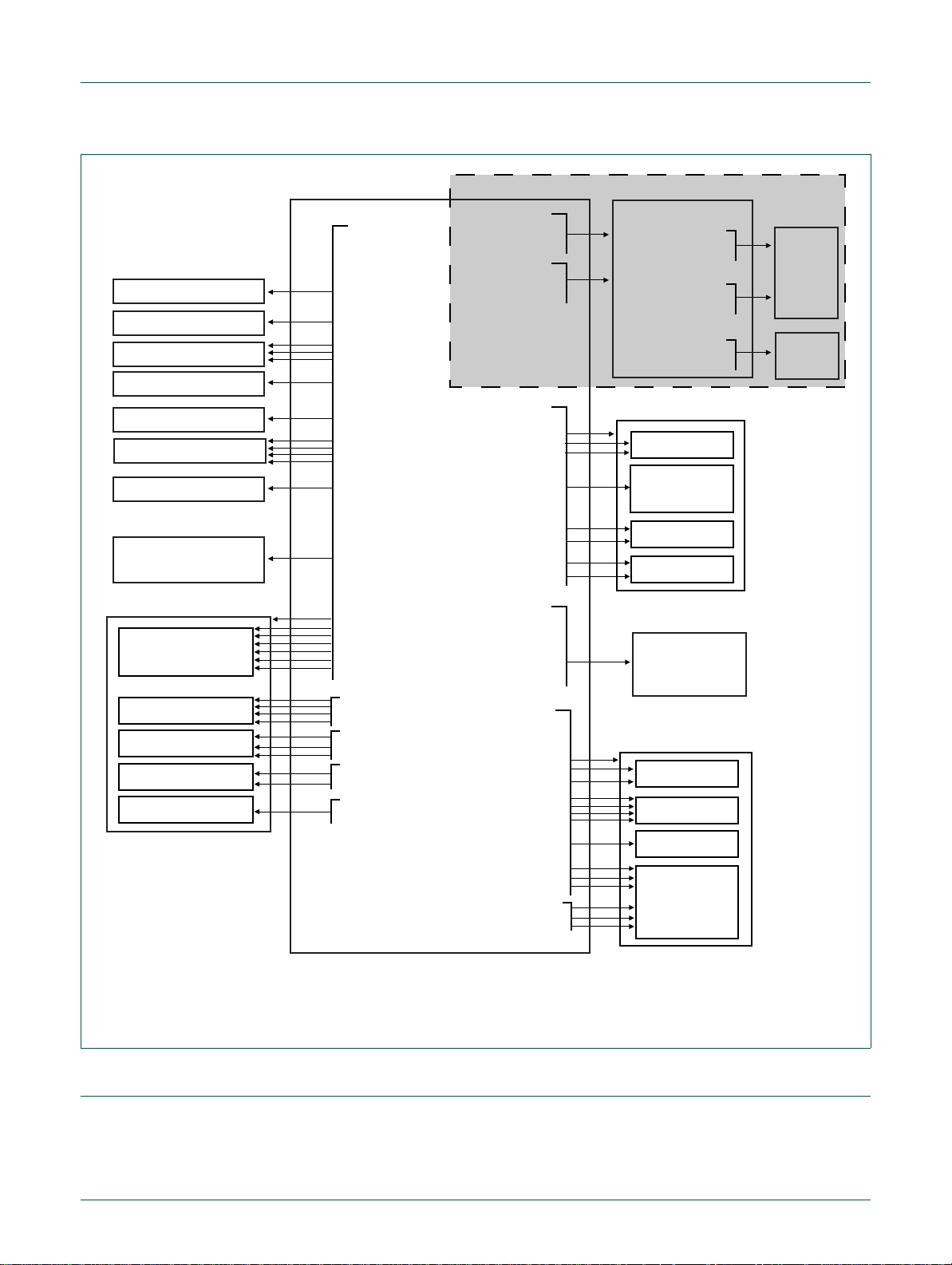
Fig 9. LPC29xx clock generation
3. CGU0 functional description
The implementation of GPIO, ADC, and memory subsystem branch clocks varies for different LPC29xx parts.
The CGU0 uses a set of building blocks to generate the clock for the output branches. The
building blocks are as follows:
UM10316_1 © NXP B.V. 2009. All rights reserved.
User manual Rev. 01.01 — 14 July 2009 25 of 568
Page 26

NXP Semiconductors
• OSC1M (LP_OSC) – 1 MHz crystal oscillator
• XO50M – up to 25 MHz oscillator
• PL160M – PLL
• FDIV0..6 – 7 Frequency Dividers
• Output control
DRAFT
D
D
RAFT DRAFT DRAFT DRAFT DRAFT D
RAFT DRA
D
RAFT
UM10316
Chapter 3: LPC29xx Clock Generation Unit (CGU)
F
T DRAFT DRAFT DRAFT DRA
DR
AFT
DRAFT
DRA
DR
AFT
DRAFT
DR
F
T DRAF
The following clock output branches are generated (Table 3–12
Table 12. CGU0 base clocks
Number Name Frequency
0 BASE_SAFE_CLK 0.4 base safe clock (always on) for WDT
1 BASE_SYS_CLK 125 base system clock; ARM and AHB clock
2 BASE_PCR_CLK 0.4
3 BASE_IVNSS_CLK 125 base IVNSS subsystem clock for
4 BASE_MSCSS_CLK 125 base MSCSS subsystem clock for
5 BASE_ICLK0_CLK 125 base internal clock 0, for CGU1
6 BASE_UART_CLK 125 base UART clock
7 BASE_SPI_CLK 50 base SPI clock
8 BASE_TMR_CLK 125 base timers clock
9 BASE_ADC_CLK 4.5 base ADCs clock
10 test clock; reserved - this is an internal clock used for testing
1 1 BASE_ICLK1_CLK 125 base internal clock 1, for CGU1
(MHz)
[2]
[1]
Description
base PCR subsystem clock; for power
control subsystem
networking subsystem (CAN, LIN, and
I2C)
modulation and sampling control
subsystem.
only. This clock is running at start-up and
should be disabled in the PMU (see
Table 5–51
configuration registers).
):
for the test shell clock
[1] Maximum frequency that guarantees stable operation of the LPC29xx.
[2] Fixed to low-power oscillator.
UM10316_1 © NXP B.V. 2009. All rights reserved.
User manual Rev. 01.01 — 14 July 2009 26 of 568
Page 27
NXP Semiconductors
400 kHz LP_OSC
PLL
FDIV0
EXTERNAL
OSCLLLATOR
FDIV1
FDIV6
OUT 0
OUT 1
OUT 11
clkout
clkout120
clkout240
CLOCK GENERATION UNIT (CGU0)
FREQUENCY MONITOR
CLOCK DETECTION
AHB TO DTL BRIDGE
BASE_SYS_CLK
BASE_ICLK1_CLK
(to CGU1)
OUT 3
BASE_IVNSS_CLK
OUT 2
BASE_PCR_CLK
BASE_SAFE_CLK
FDIV_CONF6
PLL_CONTROL
FDIV_CONF1
FDIV_CONF0
SYS_CLK_
CONF
SAFE_CLK_CONF
PCR_CLK_CONF
LP_OSC
EXT OSC
PLL clkout
PLL clkout120
PLL clkout240
FDIV0
FDIV6
LP_OSC
EXT OSC
PLL clkout
PLL clkout120
PLL clkout240
FDIV0
FDIV6
IVNSS_CLK_CONF
ICLK1_CLK_CONF
FREQ_MON
RDET
DRAFT
D
D
RAFT DRAFT DRAFT DRAFT DRAFT D
RAFT DRA
D
RAFT
UM10316
Chapter 3: LPC29xx Clock Generation Unit (CGU)
F
T DRAFT DRAFT DRAFT DRA
DR
AFT
DRAFT
DRA
DR
AFT
DRAFT
DR
F
T DRAF
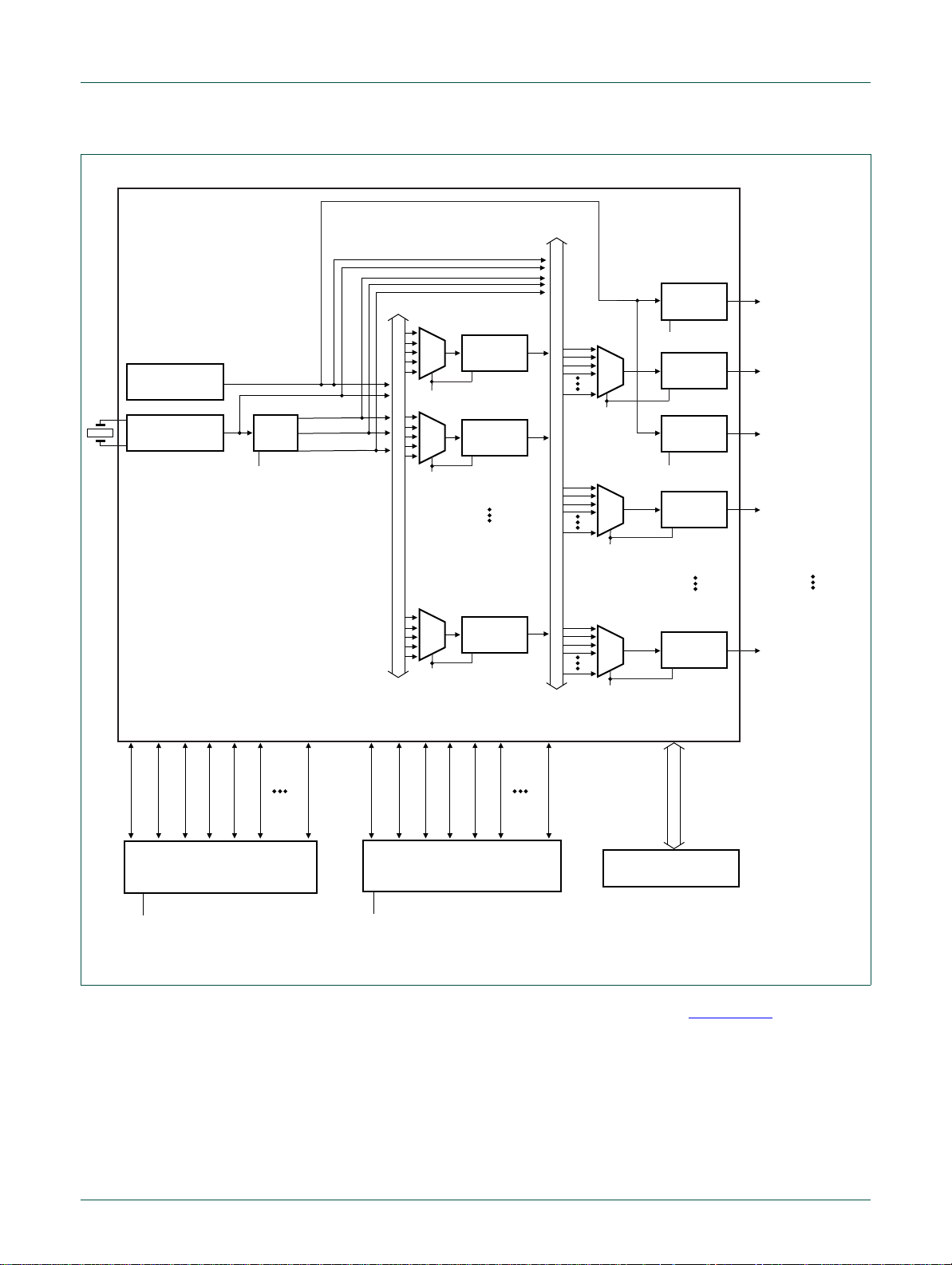
Fig 10. Schematic representation of the CGU0
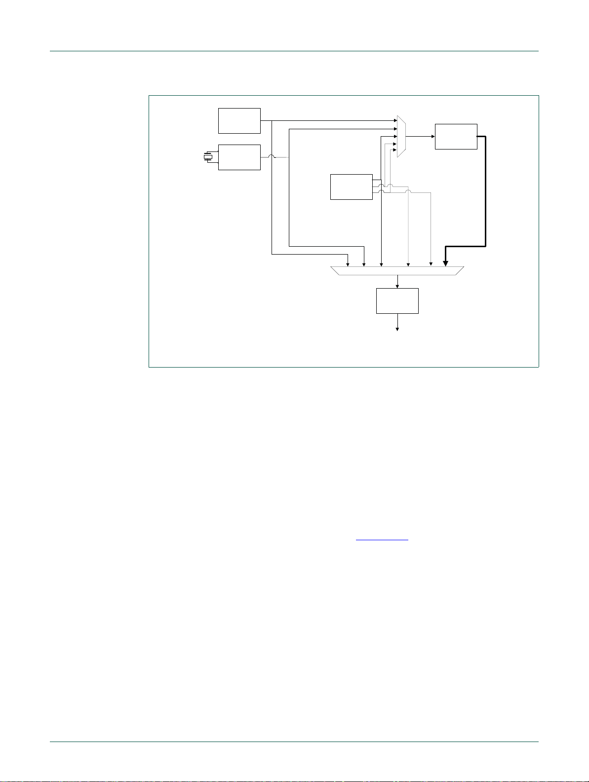
The structure of the clock path of each clock output is shown in Figure 3–11.
UM10316_1 © NXP B.V. 2009. All rights reserved.
User manual Rev. 01.01 — 14 July 2009 27 of 568
Page 28
NXP Semiconductors
OSC1M
XO50M
DRAFT
D
D
RAFT DRAFT DRAFT DRAFT DRAFT D
RAFT DRA
D
RAFT
UM10316
Chapter 3: LPC29xx Clock Generation Unit (CGU)
F
T DRAFT DRAFT DRAFT DRA
FDIV0..6
PLL160M
clkout /
clkout120 /
clkout240
Output
Control
DR
AFT
DRAFT
DRA
DR
AFT
DRAFT
DR
F
T DRAF
Clock
outputs
Fig 11. Structure of the clock generation scheme
3.1 Controlling the XO50M oscillator (external oscillator)
The XO50M oscillator can be disabled using the ENABLE field in the oscillator control
register. Even when enabled, this can be bypassed using the BYPASS field in the same
register. In this case the input of the OSC1M crystal is fed directly to the output.
The XO50M oscillator has an HF pin which selects the operating mode. For operation at
higher frequencies (15-25 MHz), the XO50M oscillator HF must be enabled. For
frequencies below that the pin must be disabl ed. Setting of the pin is contr olled b y th e HF
in the oscillator control register.
3.2 Controlling the PL160M PLL
The structure of the PLL clock path is shown in Figure 3–12.
UM10316_1 © NXP B.V. 2009. All rights reserved.
User manual Rev. 01.01 — 14 July 2009 28 of 568
Page 29
NXP Semiconductors
P23CCO
/ MDIV
clkout120 /
clkout240
/ 2PDIV
MSEL
PSEL
P23EN
Input clock
Bypass
Direct
clkout
Fig 12. PLI60MPLL control mechanisms
The PLL reference input clock is provided by the external oscillator (XO50M). The PLLs
accept an input clock frequency in the range of 10 MHz to 25 MHz only. The input
frequency can be directly routed to the post-divider using the BYPASS control. The
post-divider can be bypassed using the DIRECT control.
DRAFT
D
D
RAFT DRAFT DRAFT DRAFT DRAFT D
RAFT DRA
D
RAFT
UM10316
Chapter 3: LPC29xx Clock Generation Unit (CGU)
F
T DRAFT DRAFT DRAFT DRA
DR
AFT
DRAFT
DRA
DR
AFT
DRAFT
DR
F
T DRAF
The post-divider is controlled by settings of the field PSEL in the output control register.
PSEL is a 2-bit value that selects a division between 1 and 8 in powers of 2.
The feedback divider is controlled by settings of the MSEL field in the output control
register. The MSEL is a 5 -bit value corresponding to the feedback d ivider minus 1. Thus, if
MSEL is programmed to 0 the feedback divider is 1.
In normal mode the post-divider is enabled and the following relations are verified:
F
clkout
= MDIV × F
clkin
= F
/ 2×PDIV
cco
Values of the dividers are chosen with the following process:
1. Specify the input clock frequency F
2. Calculate M to obtain the desired output frequency F
3. Find a value for P so that F
cco
clkin
= 2×P / F
clkout
with M = F
clkout
clkout
/ F
clkin
4. Verify that all frequencies and divider values conform to the limits
In direct mode, the following relations are verified:
F
clkout
= M × F
clkin
= F
cco
Unless the PLL is configured in bypass mode it must be locked before using it as a clock
source. The PLL lock indication is read from the PLL status register.
Once the output clock is generated it is possible to use a three-phase ou tput control which
generates three clock signals separated in phase by 120°. This setting is controlled by
field P23EN.
Settings to power down the PLL, controlled by field PD in the PLL control registe r, and
safe switch setting controlled by the AUTOBLOK field are not shown in the illustration.
Note that safe switching of the clock is not enabled at reset.
UM10316_1 © NXP B.V. 2009. All rights reserved.
User manual Rev. 01.01 — 14 July 2009 29 of 568
Page 30

NXP Semiconductors
3.3 Controlling the frequency dividers
The seven frequency dividers are controlled by the FDIV0..6 registers.
The frequency divider divides the incoming clock by (L/D), where L and D are both 12-bit
values, and attempts to produce a 50% duty-cycle. Each high or low phase is stretch ed to
last approximately D/(L*2) input-clock cycles. When D/(L*2) is an integer the duty cycle is
exactly 50%, otherwise it is an approximation.
The minimum division ratio is /2, so L should always be less than or equal to D/2. If not, or
if L is equal to 0, the input clock is passed directly to the output without being divided.
3.4 Controlling the clock output
Once a source is selected for one of the clock branches the output clock can be further
sub-divided using an output divider controlled by field IDIV in the clock-output
configuration register.
Each clock-branch output can be individually controlled to power it down and perform safe
switching between clock domains. These settings are controlled by the PD and
AUTOBLOK fields respectively.
DRAFT
Chapter 3: LPC29xx Clock Generation Unit (CGU)
D
RAFT DRAFT DRAFT DRAFT DRAFT D
D
RAFT DRA
D
RAFT
UM10316
F
T DRAFT DRAFT DRAFT DRA
DR
AFT
DRAFT
DRA
DR
AFT
DRAFT
DR
F
T DRAF
The clock output can trigger disabling of the clock branch on a specific polarity of the
output. This is controlled via field RTX of the output-configuration register.
3.5 Reading the control settings
Each of the control registers is associated with a status register. These registers can be
used to read the configured controls of each of the CGU building blocks.
3.6 Frequency monitor
The CGU includes a frequency-monitor mechanism which measures the clock pulses of
one of the possible clock sources against the reference clock. The reference clock is the
PCR block clock CLK_PCR.
When a frequency-monitor measurement begins two counters are started. The first starts
from the specified number of reference-clock cycles (set in field RCNT) and counts down
to 0: the second counts cycles of the monitored frequency starting from 0. The
measurement is triggered by enabling it in field MEAS and stops either when the
reference clock counter reaches 0 or the measured clock counter (in field FCNT)
saturates.
The rate of the measured clock can be calculated using the formula:
Fmeas = Fcore × FCNTfinal / (RCNTinitial - RCNTfinal)
When the measurement is finished either FCNTfinal is equal to the saturated value of the
counter (FCNT is a 14-bit value) or RCNTfinal is zero.
Measurement accuracy is influenced by the ratio between the clocks. For greater
accuracy the frequency to measure should be closer to the reference clock.
UM10316_1 © NXP B.V. 2009. All rights reserved.
User manual Rev. 01.01 — 14 July 2009 30 of 568
Page 31

NXP Semiconductors
Configure XO50MOSC
in normal mode with
HF pin enabled
Configure PLL to use
XO50MOSC as input
and generate 80MHz
(Fin = 10 MHz
and Fcco = 160 MHz)
with 3-phase output
enabled
Wait for PLL to lock
Configure FR clock
to 40 MHz
Configure FDIV5 to use
120° PLL output and
generate ~3.6866 MHz
Configure UART_CLK
to use FDIV5 and
divide by 2
3.7 Clock detection
All of the clock sources have a clock detector, the status of which can be read in a CGU
register. This register indicates which sources have been detected.
If this is enabled, the absence of any clock source can trigger a hardware interrupt.
3.8 Bus disable
This safety feature is provided to avoid accidental changing of the clock settings. If it is
enabled, access to all registers except the RBUS register (so that it can be disabled) is
disabled and the clock settings cannot be mod ifie d.
3.9 Clock-path programming
The following flowchart shows the sequence for programing a complete clock path:
DRAFT
D
D
RAFT DRAFT DRAFT DRAFT DRAFT D
RAFT DRA
D
RAFT
UM10316
Chapter 3: LPC29xx Clock Generation Unit (CGU)
F
T DRAFT DRAFT DRAFT DRA
DR
AFT
DRAFT
DRA
DR
AFT
DRAFT
DR
F
T DRAF
Fig 13. Programming the clock path
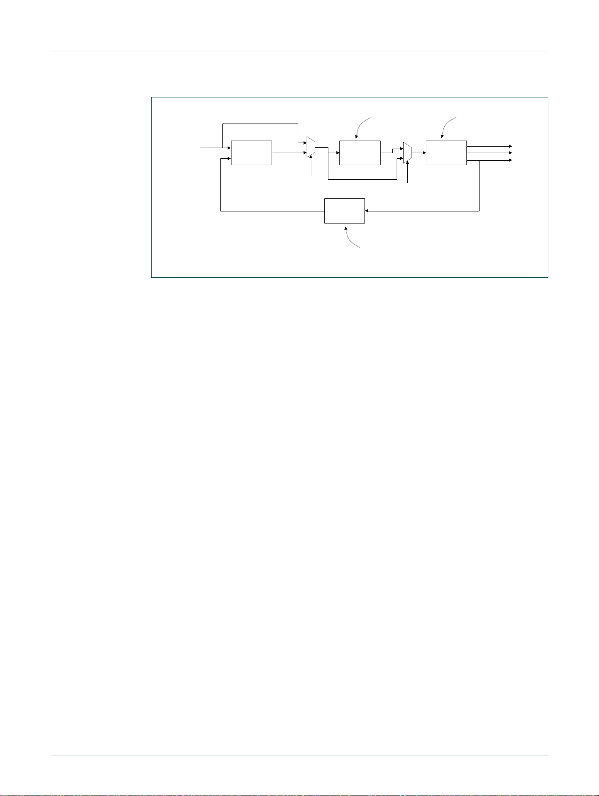
4. CGU1 functional description
The CGU1 block is functionally identical to the CGU0 block and generates two clocks for
the USB interface and a dedicated output clock. The CGU1 block uses its own PLL and
fractional dividers. The PLLs used in CGU0 and CGU1 are identical.
The clock input to the CGU1 PLL is provided by one of two base clocks generated in the
CGU0: BASE_ICLK0_CLK or BASE_INT1CLK. The base clock not used for the PLL can
be configured to drive the output clock directly.
The CGU1 provides the following three base clocks (Table 3–13
Table 13. CGU1 base clocks
Base clock Parts of the device clocked by this branch clock
UM10316_1 © NXP B.V. 2009. All rights reserved.
User manual Rev. 01.01 — 14 July 2009 31 of 568
BASE_OUT_CLK clock out pin
BASE_USB_CLK USB clock
BASE_USB_I2C_CLK USB OTG I2C clock
):
Page 32

NXP Semiconductors
PLL
FDIV0
OUT 0
OUT 2
clkout
clkout120
clkout240
CLOCK GENERATION UNIT
(CGU1)
AHB TO DTL BRIDGE
BASE_USB_CLK
BASE_OUT_CLK
OUT 1
BASE_USB_I2C_CLK
BASE_ICLK1_CLK
BASE_ICLK0_CLK
FDIV_CONF0
PLL_CONTROL
USB_CLK_CONF
USB_I2C_CLK_CONF
OUT_CLK_CONF
FREQUENCY MONITOR
CLOCK DETECTION
BASE_ICLK0_CLK
BASE_ICLK1_CLK
BASE_ICLK0_CLK
BASE_ICLK1_CLK
PLL clkout
PLL clkout120
PLL clkout240
FDIV0
PLL clkout
PLL clkout120
PLL clkout240
FDIV0
FREQ_MON
RDET
DRAFT
D
D
RAFT DRAFT DRAFT DRAFT DRAFT D
RAFT DRA
D
RAFT
UM10316
Chapter 3: LPC29xx Clock Generation Unit (CGU)
F
T DRAFT DRAFT DRAFT DRA
DR
AFT
DRAFT
DRA
DR
AFT
DRAFT
DR
F
T DRAF
5. Register overview
Table 14. Register overview: CGU0 (CGU0 base address: 0xFFFF 8000)
UM10316_1 © NXP B.V. 2009. All rights reserved.
User manual Rev. 01.01 — 14 July 2009 32 of 568
Fig 14. Block diagram of the CGU1
Name Access Address
Remark: Any clock-frequency adjustment has a direc t impact on the timing of on- bo ar d
peripherals such as the UARTs, SPI, Watchdog, timers, CAN controller, LIN master
controller, ADCs, and flash memory interface.
Description Reset value Reference
offset
- R 0x000 Reserved 0x7100 0011 -
- R 0x004 Reserved 0x0000 0000 -
- R 0x008 Reserved 0x0C00 0000 -
- R 0x00C Reserved - FREQ_MON R/W 0x014 Frequency monitor register 0x0000 0000 see Table 3–16
RDET R 0x018 Clock detection register 0x0000 0FE3 see Table 3–17
Page 33

D
RAFT
UM10316
NXP Semiconductors
DRAFT
D
D
RAFT DRAFT DRAFT DRAFT DRAFT D
RAFT DRA
Chapter 3: LPC29xx Clock Generation Unit (CGU)
F
T DRAFT DRAFT DRAFT DRA
Table 14. Register overview: CGU0 (CGU0 base address: 0xFFFF 8000) …continued
Name Access Address
offset
XTAL_OSC_STATUS R 0x01C Crystal-oscillator status register 0x0000 0001 see Table 3–18
XTAL_OSC_CONTROL R/W 0x020 Crystal-oscillator control register 0x0000 0005 see Table 3–19
PLL_STATUS R 0x024 PLL status register 0x0005 1103 see Table 3–20
PLL_CONTROL R/W 0x028 PLL control register 0x0005 1103 see Table 3–21
FDIV_STATUS_0 R 0x02C FDIV 0 frequency-divider status register 0x0000 1001 see Table 3–22
FDIV_CONF_0 R/W 0x030 FDIV 0 frequency-divider control register 0x0000 1001 see Table 3–23
FDIV_STATUS_1 R 0x034 FDIV 1 frequency-divider status register 0x0000 1001 see Table 3–22
FDIV_CONF_1 R/W 0x038 FDIV 1 frequency-divider control register 0x0000 1001 see Table 3–23
FDIV_STATUS_2 R 0x03C FDIV 2 frequency-divider status register 0x0000 1001 see Table 3–22
FDIV_CONF_2 R/W 0x040 FDIV 2 frequency-divider control register 0x0000 1001 see Table 3–23
FDIV_STATUS_3 R 0x044 FDIV 3 frequency-divider status register 0x0000 1001 see Table 3–22
FDIV_CONF_3 R/W 0x048 FDIV 3 frequency-divider control register 0x0000 1001 see Table 3–23
FDIV_STATUS_4 R 0x04C FDIV 4 frequency-divider status register 0x0000 1001 see Table 3–22
FDIV_CONF_4 R/W 0x050 FDIV 4 frequency-divider control register 0x0000 1001 see Table 3–23
FDIV_STATUS_5 R 0x054 FDIV 5 frequency-divider status register 0x0000 1001 see Table 3–22
FDIV_CONF_5 R/W 0x058 FDIV 5 frequency-divider control register 0x0000 1001 see Table 3–23
FDIV_STATUS_6 R 0x05C FDIV 6 frequency-divider status register 0x0000 1001 see Table 3–22
FDIV_CONF_6 R/W 0x060 FDIV 6 frequency-divider control register 0x0000 1001 see Table 3–23
SAFE_CLK_STATUS R 0x064 Output-clock status register for
SAFE_CLK_CONF R/W 0x068 Output-clock configuration register for
SYS_CLK_STATUS R 0x06C Output-clock status register for
SYS_CLK_CONF R/W 0x070 Output-clock configuration register for
PCR_CLK_STATUS R 0x074 Output-clock status register for
PCR_CLK_CONF R/W 0x078 Output-clock configuration register for
IVNSS_CLK_STATUS R 0x07C Output-clock status register for
IVNSS_CLK_CONF R/W 0x080 Output-clock configuration register for
MSCSS_CLK_STATUS R 0x084 Output-clock status register for
MSCSS_CLK_CONF R/W 0x088 Output-clock configuration register for
ICLK0_CLK_CONF R/W 0x08C Output-clock configuration register for
ICLK1_CLK_STATUS R 0x090 Output-clock status register for
UART_CLK_STATUS R 0x094 Output-clock status register for
UM10316_1 © NXP B.V. 2009. All rights reserved.
User manual Rev. 01.01 — 14 July 2009 33 of 568
Description Reset value Reference
0x0000 0000 see Table 3–24
BASE_SAFE_CLK
0x0000 0000 see Table 3–25
BASE_SAFE_CLK
0x0000 0000 see Table 3–26
BASE_SYS_CLK
0x0000 0000 see Table 3–27
BASE_SYS_CLK
0x0000 0000 see Table 3–26
BASE_PCR_CLK
0x0000 0000 see Table 3–27
BASE_PCR_CLK
0x0000 0000 see Table 3–26
BASE_IVNSS_CLK
0x0000 0000 see Table 3–27
BASE_IVNSS_CLK
0x0000 0000 see Table 3–26
BASE_MSCSS_CLK
0x0000 0000 see Table 3–27
BASE_MSCSS_CLK
0x0000 0000 see Table 3–26
BASE_ICLK0_CLK
0x0000 0000 see Table 3–27
BASE_ICLK0_CLK
0x0000 0000 see Table 3–26
BASE_UART_CLK
DR
AFT
DRAFT
DRA
DR
AFT
DRAFT
DR
F
T DRAF
Page 34

DR
AFT
DRAFT
NXP Semiconductors
DRAFT
D
D
RAFT DRAFT DRAFT DRAFT DRAFT D
RAFT DRA
D
RAFT
UM10316
Chapter 3: LPC29xx Clock Generation Unit (CGU)
F
T DRAFT DRAFT DRAFT DRA
Table 14. Register overview: CGU0 (CGU0 base address: 0xFFFF 8000)
Name Access Address
offset
UART_CLK_CONF R/W 0x098 Output-clock configuration register for
SPI_CLK_STATUS R 0x09C Output-clock status register for
SPI_CLK_CONF R/W 0x0A0 Output-clock configuration register for
TMR_CLK_STATUS R 0x0A4 Output-clock status register for
TMR_CLK_CONF R/W 0x0A8 Output-clock configuration register for
ADC_CLK_STATUS R 0x0AC Output-clock status register for
ADC_CLK_CONF R/W 0x0B0 Output-clock configuration register for
- R 0x0B4 reserved 0x0000 0000 -
- R/W 0x0B8 reserved 0x0000 0000 ICLK1_CLK_STATUS R 0x0BC Output-clock status register for
ICLK1_CLK_CONF R/W 0x0C0 Output-clock configuration register for
INT_CLR_ENABLE W 0xFD8 Interrupt clear-enable register 0x0000 0000 see
INT_SET_ENABLE W 0xFDC Interrupt set-enable register 0x0000 0000 see
INT_STATUS R 0xFE0 Interrupt status register 0x0000 0FE3 see
INT_ENABLE R 0xFE4 interrupt enable register 0x0000 0000 see
INT_CLR_STATUS W 0xFE8 Interrupt clear-status register 0x0000 0000 see
INT_SET_STATUS W 0xFEC Interrupt set-status register 0x0000 0000 see
- R 0xFF0 Reserved - BUS_DISABLE R/W 0xFF4 Bus disable register 0x0000 0000 see Table 3–30
- R 0xFF8 Reserved - -
- R 0xFFC Reserved 0xA0A8 1000 -
Description Reset value Reference
BASE_UART_CLK
BASE_SPI_CLK
BASE_SPI_CLK
BASE_TMR_CLK
BASE_TMR_CLK
BASE_ADC_CLK
BASE_ADC_CLK
BASE_ICLK1_CLK
BASE_ICLK1_CLK
…continued
0x0000 0000 see Table 3–27
0x0000 0000 see Table 3–26
0x0000 0000 see Table 3–27
0x0000 0000 see Table 3–26
0x0000 0000 see Table 3–27
0x0000 0000 see Table 3–26
0x0000 0000 see Table 3–27
0x0000 0000 see Table 3–26
0x0000 0000 see Table 3–27
Table 10–91
Table 10–92
Table 10–93
Table 10–94
Table 10–95
Table 10–96
DRAFT
DRA
F
DR
AFT
DR
T DRAF
Table 15. Register overview: CGU1 (CGU1 base address: 0xFFFF B000)
Name Access Address
reserved R 0x000 Reserved 0x7100 0011 reserved R 0x004 Reserved 0x0000 0000 reserved R 0x008 Reserved 0x0C00 0000 reserved R 0x00C Reserved - FREQ_MON R/W 0x014 Frequency monitor register 0x0000 0000 see Table 3–16
UM10316_1 © NXP B.V. 2009. All rights reserved.
User manual Rev. 01.01 — 14 July 2009 34 of 568
Description Reset value Reference
offset
Page 35

DR
fselected
Qselected
Qref initial[]Qref final[]–()
------------------------------------------------------------------------- -
fref×=
AFT
DRAFT
NXP Semiconductors
DRAFT
D
D
RAFT DRAFT DRAFT DRAFT DRAFT D
RAFT DRA
D
RAFT
UM10316
Chapter 3: LPC29xx Clock Generation Unit (CGU)
F
T DRAFT DRAFT DRAFT DRA
Table 15. Register overview: CGU1 (CGU1 base address: 0xFFFF B000) …continue d
Name Access Address
offset
RDET R 0x018 Clock detection register 0x0000 0FE3 see Table 3–17
PLL_STATUS R 0x01C PLL status register 0x0005 1103 see Table 3–20
PLL_CONTROL R/W 0x020 PLL control register 0x0005 1103 see Table 3–21
FDIV_STATUS_0 R 0x024 FDIV 0 frequency-divider status register 0x0000 1001 see Table 3–22
FDIV_CONF_0 R/W 0x028 FDIV 0 frequency-divider control register 0x0000 1001 see Table 3–23
USB_CLK_STATUS R 0x02C Output-clock status register for
USB_CLK_CONF R/W 0x030 Output-clock configuration register for
USB_I2C_CLK_STATUSR 0x034 Output-clock status register for
USB_I2C_CLK_CONF R/W 0x38 Output-clock configuration register for
OUT_CLK_STATUS R 0x03C Output-clock status register for
OUT_CLK_CONF R/W 0x040 Output-clock configuration register for
BUS_DISABLE R/W 0xFF4 Bus disable register 0x0000 0000 see Table 3–30
Description Reset value Reference
0x0000 0000 see Table 3–26
BASE_USB_CLK
0x0000 0000 see Table 3–27
BASE_USB_CLK
0x0000 0000 see Table 3–26
BASE_I2C_USB_CLK
0x0000 0000 see Table 3–27
BASE_I2C_USB_CLK
0x0000 0000 see Table 3–26
BASE_OUT_CLK
0x0000 0000 see Table 3–27
BASE_OUT_CLK
DRAFT
DRA
F
DR
AFT
DR
T DRAF
5.1 Frequency monitor register
The CGU can report the relative frequency of any operating clock. The clock to be
measured must be selected by software, while the fixed-frequency BASE_PCR_CLK is
used as the reference frequency. A 14-bit counter then counts the number of cycles of the
measured clock that occur during a user-defined number of re ference-clock cycles. When
the MEAS bit is set the measured-clock counter is reset to 0 and counts up, while the 9-bit
reference-clock counter is loaded with the value in RCNT and then counts down towards
0. When either counter reaches its terminal value both counters are disabled and the
MEAS bit is reset to 0. The current values of the counters can then be read out and the
selected frequency obtained by the following equation:
If RCNT is programmed to a value equal to the core clock frequency in kHz a nd reaches 0
before the FCNT counter saturates, the value stored in FCNT would then show the
measured clock’s frequency in kHz without the need for any further calculation.
Note that the accuracy of this measurement can be affected by several factors.
Quantization error is noticeable if the ratio between the two clocks is large (e.g. 100 kHz
vs. 1kHz), because one counter saturates while the other still has only a small count
value. Secondly, due to synchronization, the counters are not started and stopped at
exactly the same time. Finally, the measured frequency can only be to the same level of
precision as the reference frequency.
UM10316_1 © NXP B.V. 2009. All rights reserved.
User manual Rev. 01.01 — 14 July 2009 35 of 568
Page 36

NXP Semiconductors
Remark: The clock selection in this register depends on whether the register is used for
CGU0 or CGU1. In the CGU0, the low-power oscillator (LP_OSC) or the external crystal
oscillator can be selected as input. In the CGU1, the two CGU0 base clocks
BASE_ICLK0_CLK and BASE_ICLK1_CLK, can be selected instead. CGU1 has only one
fractional divider register.
Table 16. FREQ_MON register bit description (FREQ_MON, address 0xFFFF 8014 (CGU0)
* = reset value
Bit Symbol Access Value Description
31 to 24 CLK_SEL R/W Clock-source selection for the clock to be
23 MEAS R/W Measure frequency
22 to 9 FCNT R Selected clock-counter value
8 to 0 RCNT R/W Reference clock-counter value
and 0xFFFF B014 (CGU1))
DRAFT
D
D
RAFT DRAFT DRAFT DRAFT DRAFT D
RAFT DRA
D
RAFT
UM10316
Chapter 3: LPC29xx Clock Generation Unit (CGU)
F
T DRAFT DRAFT DRAFT DRA
measured.
0x00* LP_OSC (CGU0) or BASE_ICLK0_CLK
(CGU1)
0x01 Crystal oscillator (CGU0) or BASE_ICLK1_CLK
(CGU1)
0x02 PLL
0x03 PLL +120
0x04 PLL +240°
0x05 FDIV0 (CGU0 and CGU1)
0x06 FDIV1 (CGU0 only)
0x07 FDIV2 (CGU0 only)
0x08 FDIV3 (CGU0 only)
0x09 FDIV4 (CGU0 only)
0x0A FDIV5 (CGU0 only)
0x0B FDIV6 (CGU0 only)
0*
0x0*
0x0*
°
DR
AFT
DRAFT
DRA
DR
AFT
DRAFT
DR
F
T DRAF
5.2 Clock detection register
Each clock generator has a clock detector associated with it to alert the system if a clock
is removed or connected. The status register RDET can determine the current
‘clock-present’ status.
If enabled, interrupts are generated whenever ‘clock present’ changes status, so that an
interrupt is generated if a clock changes from ‘present’ to ‘non-present’ or from
‘non-present’ to ‘present’.
Remark: The clock selection in this register depends on whether the register is used for
CGU0 or CGU1. In the CGU0, the low-power oscillator (LP_OSC) or the external crystal
oscillator can be selected as input. In the CGU1, the two CGU0 base clocks
BASE_ICLK0_CLK and BASE_ICLK1_CLK, can be selected instead. In the CGU1, only
one fractional divider register is used.
UM10316_1 © NXP B.V. 2009. All rights reserved.
User manual Rev. 01.01 — 14 July 2009 36 of 568
Page 37

NXP Semiconductors
Table 17. RDET register bit description (RDET, address 0xFFFF 8018 (CGU0) or 0xFFFF
* = reset value
Bit Symbol Access Value Description
31 to 12 reserved R - Reserved
11 FDIV6_PRESENT R Activity-detection register for FDIV 6 (CGU0
10 FDIV5_PRESENT R Activity-detection register for FDIV 5 (CGU0
9 FDIV4_PRESENT R Activity-detection register for FDIV 4 (CGU0
8 FDIV3_PRESENT R Activity-detection register for FDIV 3 (CGU0
7 FDIV2_PRESENT R Activity-detection register for FDIV 2 (CGU0
6 FDIV1_PRESENT R Activity-detection register for FDIV 1 (CGU0
5 FDIV0_PRESENT R Activity-detection register for FDIV 0 (CGU0
4 PLL240_PRESENT R Activity-detection register for 240°-shifted
3 PLL120_PRESENT R Activity-detection register for 120°-shifted
2 PLL_PRESENT R Activity-detection register for normal PLL
B018 (CGU1))
DRAFT
D
D
RAFT DRAFT DRAFT DRAFT DRAFT D
RAFT DRA
D
RAFT
UM10316
Chapter 3: LPC29xx Clock Generation Unit (CGU)
F
T DRAFT DRAFT DRAFT DRA
only)
1* Clock present
0 Clock not present
only)
1* Clock present
0 Clock not present
only)
1* Clock present
0 Clock not present
only)
1* Clock present
0 Clock not present
only)
1* Clock present
0 Clock not present
only)
1* Clock present
0 Clock not present
and CGU1)
1* Clock present
0 Clock not present
PLL output
1* Clock present
0 Clock not present
PLL output
1* Clock present
0 Clock not present
output
1* Clock present
0 Clock not present
DR
AFT
DRAFT
DRA
DR
AFT
DRAFT
DR
F
T DRAF
UM10316_1 © NXP B.V. 2009. All rights reserved.
User manual Rev. 01.01 — 14 July 2009 37 of 568
Page 38

NXP Semiconductors
Table 17. RDET register bit description (RDET, address 0xFFFF 8018 (CGU0) or 0xFFFF
* = reset value
Bit Symbol Access Value Description
1 XTAL_PRESENT
0 LP_OSC_PRESEN
5.3 Crystal-oscillator status register (CGU0)
The register XTAL_OSC_STATUS reflects the status bits for the crystal oscillator.
Table 18. XTAL_OSC_STATUS register bit description (XTAL_OSC_STATUS, address
* = reset value
Bit Symbol Access Value Description
31 to 3 reserved R - Reserved
2 HF R Oscillator HF pin
1 BYPASS R Configure crystal operation or external clock
0 ENABLE R Oscillator-p ad enable
B018 (CGU1))
(CGU0) or
BASE_ICLK0_CLK_
PRESENT (CGU1)
T (CGU0) or
BASE_ICLK1_CLK_
PRESENT (CGU1)
0xFFFF 801C)
…continued
DRAFT
D
D
RAFT DRAFT DRAFT DRAFT DRAFT D
RAFT DRA
D
RAFT
UM10316
DRAFT
Chapter 3: LPC29xx Clock Generation Unit (CGU)
F
T DRAFT DRAFT DRAFT DRA
R Activity-detection register for crystal
-oscillator output
1* Clock present
0 Clock not present
R Activity-detection register for LP_OSC
1* Clock present
0 Clock not present
1* Oscillator high-frequency mode (crystal or
external clock source above 10 MHz)
0 Oscillator low-frequency mode (crystal or
external clock source below 20 MHz)
input pin XIN_OSC
0 Operation with crystal connected
1* Bypass mode. Use this mode when an external
clock source is used instead of a crystal
0 Power-down
1* Enable
DR
AFT
DRA
DR
AFT
DRAFT
DR
F
T DRAF
5.4 Crystal oscillator control register (CGU0)
The register XTAL_OSC_CONTROL contains the control bits for the crystal oscillator.
Following a change of ENABLE bit in XTAL_OSC_CONTROL register requires a read in
XTAL_OSC_STATUS to confirm ENABLE bit is indeed changed.
T able 19. XTAL_OSC_CONTROL register bit description (XTAL_OSC_CONTROL, address
0xFFFF 8020)
* = reset value
Bit Symbol Access Value Description
31 to 3 reserved R - Reserved
UM10316_1 © NXP B.V. 2009. All rights reserved.
User manual Rev. 01.01 — 14 July 2009 38 of 568
Page 39

NXP Semiconductors
T able 19. XTAL_OSC_CONTROL register bit description
* = reset value
Bit Symbol Access Value Description
2 HF R/W Oscillator HF pin
1 BYPASS R/W Configure crystal operation or external-clock
0 ENABLE R/W Oscillator-pad enable
address 0xFFFF 8020)
DRAFT
D
D
RAFT DRAFT DRAFT DRAFT DRAFT D
RAFT DRA
D
RAFT
UM10316
Chapter 3: LPC29xx Clock Generation Unit (CGU)
F
T DRAFT DRAFT DRAFT DRA
…continued(XTAL_OSC_CONTROL,
1* Oscillator high-frequency mode (crystal or
external clock source 15 to 25 MHz)
0 Oscillator low-frequency mode (crystal or
external clock source 1 to 20 MHz)
input pin XIN_OSC
0* Operation with crystal connected
1 Bypass mode. Use this mode when an external
clock source is used instead of a crystal
0 Power-down
1* Enable
[1]
[1]
DR
AFT
DRAFT
DRA
[2]
[2]
DR
AFT
DRAFT
DR
F
T DRAF
[1] Do not change the BYPASS and ENABLE bits in one write-action: this will result in unstable device
operation!
[2] For between 15 MHz to 20 MHz the state of the HF pin is don’t care, see also the crystal specification notes
in Ref. 31–1
. Section 11 (Oscillator).
5.5 PLL status register (CGU0 and CGU1)
The register PLL_STATUS reflects the status bits of the PLL.
Table 20. PLL_STATUS register bit description (PLL_STATUS, address 0xFFFF 8024
(CGU0) and 0xFFFF B024 (CGU1))
* = reset value
Bit Symbol Access Value Description
31 to 1 reserved R - Reserved; do not modify. Read as logic 0, write
as logic 0
0 LOCK R Indicates if the PLL is in lock or not.
1In lock
0* Not in lock
5.6 PLL control register (CGU0 and CGU1)
The PLL_CONTROL register contains the control bits for the PLL. In the CGU0, only the
crystal oscillator is allowed as an input to the PLL. In the CGU1, both internal base clocks,
BASE_ICLK0_CLK and BASE_ICLK1_CLK, can be inputs to the PLL.
Post-divider ratio programming
The division ratio of the post-divider is controlled by PSEL[0:1] in the PLL_CONTROL
register. The division ratio is twice the value of P. This guarantees an output clock with a
50% duty cycle.
Feedback-divider ratio programming
UM10316_1 © NXP B.V. 2009. All rights reserved.
User manual Rev. 01.01 — 14 July 2009 39 of 568
Page 40

NXP Semiconductors
fclkoutPLL Mfclkin
fcco
2P⋅()
--------------- -
==
fclkout Mfclkin fcco==
The feedback-divider division ratio is controlle d by M SEL[ 4: 0] in the PLL _ CON T ROL
register. The divisio n ratio between the PLL output clock and the input clock is the decimal
value on MSEL[4:0] plus one.
Frequency selection, mode 1 (normal mode)
In this mode the post-divider is enabled, giving a 50% duty cycle clock with the frequency
relations described below:
The output frequency of the PLL is given by the following equation:
To select the appropriate values for M and P:
DRAFT
D
D
RAFT DRAFT DRAFT DRAFT DRAFT D
RAFT DRA
D
RAFT
UM10316
Chapter 3: LPC29xx Clock Generation Unit (CGU)
F
T DRAFT DRAFT DRAFT DRA
DR
AFT
DRAFT
DRA
DR
AFT
DRAFT
DR
F
T DRAF
1. Specify the input clock frequency f
2. Calculate M to obtain the desired output frequency f
3. Find a value for P so that f
cco
clkin
= 2 × P × f
clkout
clkout PLL
with M = f
clkout/fclkin
4. Verify that all frequencies and divider values conform to the limits specified.
Frequency selection, mode 2 (direct CCO mode)
In this mode the post-divider is bypassed and the CCO clock is sent directly to the
output(s), leading to the following frequency equation:
To select the appropriate values for M and P:
1. Specify the input clock frequency f
2. Calculate M to obtain the desired output frequency f
clkin
clkout
with M = f
clkout/fclkin
3. Verify that all frequencies and divider values conform to the limits specified.
Note that although the post-divider is not used, it still runs in this mode. To reduce current
consumption to the lowest possible value it is recommended to set PSEL[1:0] to ’00’. This
sets the post-divider to divide by two, which causes it to consume the least amount of
current.
T able 21. PLL_CONTROL register bit description (PLL_CONTROL, address 0xFFFF 8028
(CGU0) and 0xFFFF B028 (CGU1))
* = reset value
Bit Symbol Access Value Description
31 to 24 CLK_SEL R/W Clock-source Selection for clock generator to
be connected to the input of the PLL.
0x00* Not used (CGU0) or BASE_ICLK0_CLK
(CGU1)
0x01 Crystal oscillator (CGU0) or BASE_ICLK1_CLK
(CGU1)
0x02 to
0xFF
Not used
UM10316_1 © NXP B.V. 2009. All rights reserved.
User manual Rev. 01.01 — 14 July 2009 40 of 568
Page 41

NXP Semiconductors
T able 21. PLL_CONTROL register bit description (PLL_CONTROL, address 0xFFFF 8028
* = reset value
Bit Symbol Access Value Description
23 to 16 MSEL[4:0] R/W Feedback-divider division ratio (M)
15 to 12 reserved R Reserved
11 AUTOBLOK W 1 Enables auto-blocking of clock when
10 reserved R - Reserved
9 and 8 PSEL[1:0] R/W Post-divider division ratio (2P)
7 DIRECT R/W Direct CCO clock output control
6 to 3 reserved R Reserved
7 to 3 reserved R Reserved
2 P23EN R/W Three-phase output mode control
1 BYPASS R/W Input-clock bypass control
0 PD R/W Power-down control
Chapter 3: LPC29xx Clock Generation Unit (CGU)
(CGU0) and 0xFFFF B028 (CGU1)) …continued
00000 1
00001 2
00010 3
00011 4
00100* 5
::
11111 32
programming changes
0 No action
00 2
01* 4
10 8
11 16
0* Clock output goes through post-divider
1 Clock signal goes directly to outputs
0* PLL +120° and PLL +240
1 PLL +120
0 CCO clock sent to post-dividers (only for test
modes)
1* PLL input clock sent to post-dividers
0 Normal mode
1* Power-down mode
DRAFT
°
and PLL +240° outputs enabled
D
RAFT DRAFT DRAFT DRAFT DRAFT D
D
RAFT DRA
[2]
D
RAFT
UM10316
F
[1]
°
outputs disabled
DRAFT
T DRAFT DRAFT DRAFT DRA
[1]
DR
AFT
DRA
DR
AFT
DRAFT
DR
F
T DRAF
[1] Changing the divider ratio while the PLL is running is not recommended. Since there is no way of
synchronizing the change of the MSEL and PSEL values with the divider the risk exists that the counter will
read in an undefined value, which could lead to unwanted spikes or drops in the frequency of the output
clock. The recommended way of changing between divider settings is to power down the PLL, adjust the
divider settings and then let the PLL start up again.
[2] To power down the PLL, P23EN bit should also be set to 0.
UM10316_1 © NXP B.V. 2009. All rights reserved.
User manual Rev. 01.01 — 14 July 2009 41 of 568
Page 42

NXP Semiconductors
5.7 Frequency divider status register
There is one status register FDIV_STATUS_n for each frequency divider (n = 0..6 for
CGU0). Note that there is only one frequency divider in the CGU1. The status bits reflect
the inputs to the FDIV as driven from the control register
Table 22. FDIV_STATUS_n register bit description (FDIV_STATUS_0 to 6, address 0xFFFF
* = reset value
Bit Symbol Access Value Description
31 to 24 CLK_SEL R Selected source clock for FDIV n
23 to 12 LOAD R Load value
11 to 0 DENOMINATOR R Denominator or modulo value.
DRAFT
D
D
RAFT DRAFT DRAFT DRAFT DRAFT D
RAFT DRA
D
RAFT
UM10316
DR
DRAFT
Chapter 3: LPC29xx Clock Generation Unit (CGU)
F
T DRAFT DRAFT DRAFT DRA
802C/34/3C/44/4C/54/5C (CGU0) and FDIV_STATUS_0, address 0xFFFF B024
(CGU1))
0x00h* LP_OSC (CGU0) or (BASE_ICLK0_CLK)
(CGU1)
0x01h Crystal oscillator (CGU0) or
(BASE_ICLK1_CLK) (CGU1)
0x02h PLL
0x03h PLL +120
0x04h PLL +240
0x05 to
0xFF
0x1*
0x1*
Not used
0
0
AFT
DRA
DR
AFT
DRAFT
DR
F
T DRAF
5.8 Frequency divider configuration register
There is one control register FDIV_CONF_n for each frequency divider (n = 0..6).
The frequency divider divides the incoming clock by (LOAD/DENOMINATOR), where
LOAD and DENOMINATOR are both 12-bit values programmed in the control register
FDIV_CONTROL_n.
Essentially the output clock generates ‘LOAD’ positive edges during every
‘DENOMINATOR’ cycle of the input clock. An attempt is made to produce a 50%
duty-cycle. Each high or low phase is stretched to last approximately
DENOMINATOR/(LOAD*2) input clock cycles. When DENOMINATOR/(LOAD*2) is an
integer the duty cycle is exactly 50%: otherwise the waveform will only be an
approximation. It will be close to 50% for relatively large non-integer values of
DENOMINATOR/(LOAD*2), but not for small values.
The minimum division ratio is divide-by-2, so LOAD should always be less than or equal to
(DENOMINATOR/2). If this is not true, or if LOAD is equal to 0, the input clock is passed
directly to the output with no division.
UM10316_1 © NXP B.V. 2009. All rights reserved.
User manual Rev. 01.01 — 14 July 2009 42 of 568
Page 43

NXP Semiconductors
Table 23. FDIV_CONF_n register bit description (FDIV_CONF_n, address 0xFFFF
* = reset value
Bit Symbol Access Value Description
31 to 24 CLK_SEL R/W Selected source clock for FDIV n
23 to 12 LOAD R/W Load value
11 to 0 DENOMINATOR R/W Denominator or modulo value.
DRAFT
D
D
RAFT DRAFT DRAFT DRAFT DRAFT D
RAFT DRA
D
RAFT
UM10316
Chapter 3: LPC29xx Clock Generation Unit (CGU)
F
T DRAFT DRAFT DRAFT DRA
8030/38/40/48/50/58/60 (CGU0) and FDIV_CONF_0, address 0xFFFF B028 (CGU1))
0x00h* LP_OSC (CGU0) or (BASE_ICLK0_CLK)
(CGU1)
0x01h Crystal oscillator (CGU0) or
(BASE_ICLK1_CLK) (CGU1)
0x02h PLL
0x03h PLL +120
0x04h PLL +240
0x05 to
0xFF
0x1*
0x1*
Invalid
0
0
DR
AFT
DRAFT
DRA
DR
AFT
DRAFT
DR
F
T DRAF
5.9 Output-clock status register for BASE_SAFE_CLK and BASE_PCR_CLK
There is one status register for each CGU output clock generated. All output generators
have the same register bits. Exceptions are the output generators for BASE_SAFE_CLK
and BASE_PCR_CLK, which are described here. For the other outputs, see
Section 3–5.11
T able 24. SAFE_CLK_STA TUS (address 0xFFFF 8064), PCR_CLK_ST A TUS (address 0xFFFF
* = reset value
Bit Symbol Access Value Description
31 to 5 reserved R - Reserved
4 to 2 IDIV R 000* In teger divide value
1 to 0 reserved R - Reserved.
.
0074) register bit description
5.10 Output-clock configuration register for BASE_SAFE_CLK and BASE_PCR_CLK
There is one configuration register for each CGU output clock generated. All output
generators have the same register bits. An exception is the output generators for
BASE_SAFE_CLK and BASE_PCR_CLK, which are described here. For the other
outputs see Section 3–5.12
.
UM10316_1 © NXP B.V. 2009. All rights reserved.
User manual Rev. 01.01 — 14 July 2009 43 of 568
Page 44

NXP Semiconductors
Table 25. SAFE_CLK_CONF (address 0xFFFF 8068), PCR_CLK_CONF (address 0xFFFF
* = reset value
Bit Symbol Access Value Description
31 to 24 CLK_SEL R/W Selected source clock
23 to 5 reserved R - Reserved; do not modify, read as logic 0, write
4 to 2 IDIV R/W 000* Integer divide va lue
1 to 0 reserved R - Reserved; do not modify. Read as logic 0, write
5.1 1 Output-clock status register for CGU0 clocks
Chapter 3: LPC29xx Clock Generation Unit (CGU)
8078) register bit description
0x0* LP_OSC
0x01 to
0xFF
DRAFT
Invalid: the hardware will not accept these
values when written
as logic 0
as logic 0
D
RAFT DRAFT DRAFT DRAFT DRAFT D
D
RAFT DRA
D
RAFT
UM10316
F
T DRAFT DRAFT DRAFT DRA
DR
DRAFT
AFT
DRA
DR
AFT
DRAFT
DR
F
T DRAF
There is one status register for each CGU output clock generated. All output generators
have the same register bits. Exceptions are the output generators for BASE_SAFE_CLK
and BASE_PCR_CLK, see Section 3–5.9
Table 26. XX_CLK_STATUS register bit description (XX = SYS (address 0xFFFF 806C),
IVNSS (address 0xFFFF 807C), MSCSS (address 0xFFFF 8084), UART (address
0xFFFF 8094), SPI (address 0xFFFF 809C), TMR (address 0xFFFF 80A4), ADC
(address 0xFFFF 80AC))
* = reset value
Bit Symbol Access Value Description
31 to 5 reserved R - Reserved
4 to 2 IDIV R 000* In teger divide value
1 RTX R 0* Clock-disable polarity
0 PD R 0* Power-down clock slice
.
5.12 Output-clock configuration register for CGU0 clocks
There is one configuration register for each CGU output clock generated. All output
generators have the same register bits. Exceptions are the output generators for
BASE_SAFE_CLK and BASE_PCR_CLK, see Section 3–5.10
XX = SYS, IVNSS, MSCSS, UART, SPI, TMR or ADC, ICLK0/1_CLK
Each output generator takes in one input clock and sends one clock out of the CGU. In
between the clock passes through an integer divider and a clock control block. A clock
blocker/switch block connects to the clock control block.
.
The integer divider has a 3-bit control signal, IDIV, and divides the incoming clock by any
value from 1 through 8. The divider value is equal to (IDIV + 1); if IDIV is equal to zero, the
incoming clock is passed on directly to the next stage. When the input to the integer
divider has a 50% duty cycle the divided output will have a 50% duty cycle for all divide
values. If the incoming duty cycle is not 50% only even divide values will produce an
output clock with a 50% duty cycle.
UM10316_1 © NXP B.V. 2009. All rights reserved.
User manual Rev. 01.01 — 14 July 2009 44 of 568
Page 45

NXP Semiconductors
Table 27. XX_CLK_CONF register bit description (XX = SYS (address 0xFFFF 8070), IVNSS
* = reset value
Bit Symbol Access Value Description
31 to 24 CLK_SEL R/W selected source clock
23 to 12 reserved R - Reserved
11 AUTOBLOK W - Enables auto-blocking of clock when
10 to 5 reserved R - Reserved; do not modify. Read as logic 0, write
4 to 2 IDIV R/W 000* Integer divide va lue
1 reserved R/W 0* Reserved; do not modify. Read as logic 0, write
0 PD R/W 0* Power-down clock slice
DRAFT
D
D
RAFT DRAFT DRAFT DRAFT DRAFT D
RAFT DRA
D
RAFT
UM10316
Chapter 3: LPC29xx Clock Generation Unit (CGU)
F
T DRAFT DRAFT DRAFT DRA
(address 0xFFFF 8080), MSCSS (address 0xFFFF 8088), UART (address 0xFFFF
8098), SPI (address 0xFFFF 80A0), TMR (address 0xFFFF 80A8), ADC (address
0xFFFF 80B0))
0x00* LP_OSC
0x01 Crystal oscillator
0x02 PLL
0x03 PLL +120
0x04 PLL +240
0x05 FDIV0
0x06 FDIV1
0x07 FDIV2
0x08 FDIV3
0x09 FDIV4
0x0A FDIV5
0x0B FDIV6
programming changes
as logic 0
as logic 0
[1]
0
0
DR
AFT
DRAFT
DRA
DR
AFT
DRAFT
DR
F
T DRAF
[1] At reset release, the JTAGSEL pin is sampled. If it is LOW (ARM debug), the crystal oscillator (XO50M) will
be selected as source for BASE_SYS_CLK.
5.13 Output-clock status register for CGU1 clocks
There is one status register for each CGU1 output clock generated. All output generators
have the same register bits.
Table 28. XX_CLK_STATUS register bit description (XX = USB_CLK (addr ess 0xFFFF
B02C), USB_I2C (address 0xFFFF B034), OUT_CLK (address 0xFFFF B03C))
* = reset value
Bit Symbol Access Value Description
31 to 5 reserved R - Reserved
4 to 2 IDIV R 000* In teger divide value
1 RTX R 0* Clock-disable polarity
0 PD R 0* Power-down clock slice
UM10316_1 © NXP B.V. 2009. All rights reserved.
User manual Rev. 01.01 — 14 July 2009 45 of 568
Page 46

NXP Semiconductors
5.14 Output-clock configuration register for CGU1 clocks
There is one configuration register for each CGU1 output clock generated. All output
generators have the same register bits. The CG U1 output clo ck can be generated directly
from the two CGU0 base clocks BASE_ICLK0_CLK and BASE_ICLK1_CLK or from the
CGU1 PLL.
Each output generator takes in one input clock and sends one clock out of the CGU. In
between the clock passes through an integer divider and a clock control block. A clock
blocker/switch block connects to the clock control block.
The integer divider has a 3-bit control signal, IDIV, and divides the incoming clock by any
value from 1 through 8. The divider value is equal to (IDIV + 1); if IDIV is equal to zero, the
incoming clock is passed on directly to the next stage. When the input to the integer
divider has a 50% duty cycle the divided output will have a 50% duty cycle for all divide
values. If the incoming duty cycle is not 50% only even divide values will produce an
output clock with a 50% duty cycle.
Table 29. XX_CLK_CONF register bit description (XX = USB_CLK (address 0xFFFF B030),
* = reset value
Bit Symbol Access Value Description
31 to 24 CLK_SEL R/W selected source clock
23 to 12 reserved R - Reserved
11 AUTOBLOK W - Enables auto-blocking of clock when
10 to 5 reserved R - Reserved; do not modify. Read as logic 0, write
4 to 2 IDIV R/W 000* Integer divide value
1 reserved R/W 0* Reserved; do not modify. Read as logic 0, write
0 PD R/W 0* Power-down clock slice
DRAFT
D
D
RAFT DRAFT DRAFT DRAFT DRAFT D
RAFT DRA
D
RAFT
UM10316
DRAFT
Chapter 3: LPC29xx Clock Generation Unit (CGU)
F
T DRAFT DRAFT DRAFT DRA
USB_I2C_CLK (address 0xFFFF B038), OUT_CLK (address 0xF FFF B040))
0x00* BASE_ICLK0_CLK
0x01 BASE_ICLK1_CLK
0x02 PLL
0x03 PLL +120
0x04 PLL +240
0x05 FDIV0
0x06 -
0x0B
reserved
programming changes
as logic 0
as logic 0
0
0
DR
AFT
DRA
DR
AFT
DRAFT
DR
F
T DRAF
[1] When JTAG = 1, crystal Oscillator will be the default value for the BASE_SYS_CLK
5.15 Bus disable register
The BUS_DISABLE register prevents any disabled register in the CGU0 from being
written to.
UM10316_1 © NXP B.V. 2009. All rights reserved.
User manual Rev. 01.01 — 14 July 2009 46 of 568
Page 47

NXP Semiconductors
T able 30. BUS_DISABLE register bit description (BUS_DISABLE, address 0xFFFF 8FF4
* = reset value
Bit Symbol Access Value Description
31 to 1 reserved R - Reserved; do not modify. Read as logic 0, write
0 RRBUS R/W Bus write-disable bit
5.16 CGU0 interrupt bit description
Table 3–31 gives the interrupts for the CGU0. The first column gives the bit number in the
interrupt registers. For a general explanation of the interrupt concept and a description of
the registers see Section 10–5
Table 31. CGU interrupt sources
Register
bit
31 to 12 unused Unused
11 FDIV6 FDIV 6 activity state change
10 FDIV5 FDIV 5 activity state change
9 FDIV4 FDIV 4 activity state change
8 FDIV3 FDIV 3 activity state change
7 FDIV2 FDIV 2 activity state change
6 FDIV1 FDIV 1 activity state change
5 FDIV0 FDIV 0 activity state change
4 PL160M240 PLL +240° activity state change
3 PL160M120 PLL +120° activity state change
2 PL160M PLL activity state change
1 crystal Crystal-oscillator activity state change
0 LP_OSC Ring-oscillator activity state change
Chapter 3: LPC29xx Clock Generation Unit (CGU)
(CGU0) and 0xFFFF BFF4 (CGU1))
as logic 0
1 No writes to registers within CGU are possible
(except the BUS_DISABLE register)
0* Normal operation
.
Interrupt source Description
DRAFT
D
AFT
DRA
DR
AFT
DRAFT
DR
F
T DRAF
D
RAFT DRAFT DRAFT DRAFT DRAFT D
RAFT DRA
D
RAFT
UM10316
F
T DRAFT DRAFT DRAFT DRA
DR
DRAFT
UM10316_1 © NXP B.V. 2009. All rights reserved.
User manual Rev. 01.01 — 14 July 2009 47 of 568
Page 48

UM10316
Chapter 4: LPC29xx Reset Generation Unit (RGU)
Rev. 01.01 — 14 July 2009 User manual
1. How to read this chapter
The contents of this chapter apply to all LPC29xx part s. The USB re set is not available on
the LPC2917/19/01 parts.
2. Introduction
The RGU is part of the Power Control, Clock, and Reset Subsystem (PCRSS) together
with the CGU (see Section 3–3
3. RGU functional description
) and PMU.
DRAFT
D
AFT
DRA
DR
AFT
DRAFT
DR
F
T DRAF
D
RAFT DRAFT DRAFT DRAFT DRAFT D
D
RAFT
RAFT DRA
F
T DRAFT DRAFT DRAFT DRA
DR
DRAFT
The RGU allows generation of independent reset signals for the following outputs:
Table 32. Reset output configuration
Reset output Reset source Parts of the device reset when activated
POR_RST power-on reset module LP_OSC; source for RGU_RST
RGU_RST POR_RST, RST_N pin RGU internal; source for PCR_RST
PCR_RST RGU_RST, WATCHDOG PCR (Power, Clock, and Reset) internal;
source for COLD_RST
COLD_RST PCR_RST parts with COLD_RST as reset source below
WARM_RST COLD_RST parts with WARM_RST as reset source below
SCU_RST COLD_RST SCU
CFID_RST COLD_RST CFID
FMC_RST COLD_RST embedded Flash-Memory Controller (FMC)
EMC_RST COLD_RST embedded SRAM-Memory Controller
SMC_RST COLD_RST external Static-Memory Controller (SMC)
GESS_A2V_RST WARM_RST GeSS AHB-to-APB bridge
PESS_A2V_RST WARM_RST PeSS AHB-to-APB bridge
GPIO_RST WARM_RST all GPIO modules
UART_RST WARM_RST all UART modules
TMR_RST WARM_RST all Timer modules in PeSS
SPI_RST WARM_RST all SPI modules
IVNSS_A2V_RST WARM_RST IVNSS AHB-to-APB bridge
IVNSS_CAN_RST WARM_RST all CAN modules including Acceptance filter
IVNSS_LIN_RST WARM_RST all LIN modules
MSCSS_A2V_RST WARM_RST MSCSS AHB to APB bridge
MSCSS_PWM_RST WARM_RST all PWM modules
MSCSS_ADC_RST WARM_RST all ADC modules
MSCSS_TMR_RST WARM_RST all Timer modules in MSCSS
I2C_RST WARM_RST all I2C modules
UM10316_1 © NXP B.V. 2009. All rights reserved.
User manual Rev. 01.01 — 14 July 2009 48 of 568
Page 49

NXP Semiconductors
Table 32. Reset output configuration
Reset output Reset source Parts of the device reset when activated
QEI_RST WARM_RST Quadrature encoder
DMA_RST WARM_RST GPDMA controller
USB_RST WARM_RST USB controller
VIC_RST WARM_RST Vectored Interrupt Controller (VIC)
AHB_RST WARM_RST CPU and AHB Bus infrastructure
Generation of reset outputs is controlled using registers RESET_CTRL0 and
RESET_CTRL1. Note that a POR reset can also be triggered by software.
The RGU monitors the reset cause for each reset output. The reset cause can be
retrieved with two levels of granularity.
The first level is monitored by the RESET_STATUS0 to 3 registers and indicates one of
the following reset causes (see Table 4–37
DRAFT
Chapter 4: LPC29xx Reset Generation Unit (RGU)
…continued
to Table 4–40):
D
RAFT DRAFT DRAFT DRAFT DRAFT D
D
RAFT DRA
D
RAFT
UM10316
F
T DRAFT DRAFT DRAFT DRA
DR
AFT
DRAFT
DRA
DR
AFT
DRAFT
DR
F
T DRAF
• No reset has taken place
• Watchdog reset
• Reset generated by software via RGU register
• Other cause
The second level of granularity is monitored by one individual register for each reset
output in which the detailed reset cause is indicated (see Table 4–43
Detailed reset causes depend on the reset hierarchy:
to Table 4–47).
• POR reset (does not have a reset source register as it can only be activated by POR)
• RGU reset
• Watchdog reset
• PCR (Power control, Clock, and Reset Subsystem) reset
• Cold reset
• Warm reset
3.1 Reset hierarchy
The different types of system reset can be ordered according to their sco pe. The hierarchy
is as follows (see Table 4–33
1. POR reset: resets everything in the microcontroller.
2. External reset: resets everything in the microcontroller except the OSC 1M oscillator.
3. RGU reset: resets RGU and then has the same effect as Watchdog reset.
4. Watchdog-triggered reset: triggers PCR reset.
5. PCR reset: triggers cold reset and resets Watchdog and flash controller.
6. Cold reset: triggers warm reset and resets GPIO, external memory controller, flash
controller, SRAM controller, the SCU, and the CFID.
7. Warm reset: Resets non-memory peripherals (UART, ADC, I2C, timers, etc.). Does
not reset memory controllers, SCU, CFID or Watchdog.
):
UM10316_1 © NXP B.V. 2009. All rights reserved.
User manual Rev. 01.01 — 14 July 2009 49 of 568
Page 50

DR
DRAFT
NXP Semiconductors
DRAFT
D
D
RAFT DRAFT DRAFT DRAFT DRAFT D
RAFT DRA
D
RAFT
UM10316
Chapter 4: LPC29xx Reset Generation Unit (RGU)
F
Table 33. Reset priority
Priority Reset OSC1M RGU WDT GPIO SCU Flash
1 POR yes yes yes yes yes yes yes yes yes
2 EXT
RESET
3 RGU no yes yes yes yes yes yes yes yes
4 WDT no no yes yes yes yes yes yes yes
5 PCR no no yes yes yes yes yes yes yes
6 Cold no no no yes yes yes yes yes yes
7 Warmnononononono nono yes
CFID Memory
controller
no yes yes yes yes yes yes yes yes
controllers
(SRAM,SMC)
T DRAFT DRAFT DRAFT DRA
all other
peripherals
4. Register overview
AFT
DRA
DR
AFT
DRAFT
DR
F
T DRAF
Table 34. Register overview: RGU (base address: 0xFFFF 9000)
Name Access Address
RESET_CTRL0 W 0x100 Reset control register 0 - see Table 4–35
RESET_CTRL1 W 0x104 Reset control register 1 - see Table 4–36
RESET_STATUS0 R/W 0x110 Reset status register 0 0x140 see Table 4–37
RESET_STATUS1 R/W 0x114 Reset status register 1 0x0 see Table 4–38
RESET_STATUS2 R/W 0x118 Reset status register 2 0x5555 5555 see Table 4–39
RESET_STATUS3 R/W 0x11C Reset status register 3 0x5555 5555 see Table 4–40
RST_ACTIVE_STATUS0 R 0x150 Reset-Active Status register 0 0xFFFF
RST_ACTIVE_STATUS1 R 0x154 Reset-Active Status register 1 0xFFFF
RGU_RST_SRC R/W 0x404 Source register for RGU reset 0x0000 0000 see Table 4–43
PCR_RST_SRC R/W 0x408 Source register for PCR reset 0x0000 0000 see Table 4–44
COLD_RST_SRC R/W 0x40C Source register for COLD reset 0x0000 0010 see Table 4–45
WARM_RST_SRC R/W 0x410 Source register for WARM reset 0x0000 0020 see Table 4–46
SCU_RST_SRC R/W 0x480 Source register for SCU reset 0x0000 0020 see Table 4–46
CFID_RST_SRC R/W 0x484 Source register for CFID reset 0x0000 0020 see Table 4–46
FMC_RST_SRC R/W 0x490 Source register for EFC reset 0x0000 0020 see Table 4–46
EMC_RST_SRC R/W 0x494 Source register for EMC reset 0x0000 0020 see Table 4–46
SMC_RST_SRC R/W 0x498 Source register for SMC reset 0x0000 0020 see Table 4–46
GESS_A2V_RST_SRC R/W 0x4A0 Source register for GeSS AHB2APB
PESS_A2V_RST_SRC R/W 0x4A4 Source register for PeSS AHB2APB
GPIO_RST_SRC R/W 0x4A8 Source register for GPIO reset 0x0000 0040 see Table 4–47
UART_RST_SRC R/W 0x4AC Source register for UART reset 0x0000 0040 see Table 4–47
TMR_RST_SRC R/W 0x4B0 Source register for Timer reset 0x0000 0040 see Table 4–47
SPI_RST_SRC R/W 0x4B4 Source register for SPI reset 0x0000 0040 see Table 4–47
Description Reset value Reference
offset
see Table 4–41
FFFF
see Table 4–42
FFFF
0x0000 0040 see Table 4–47
bridge reset
0x0000 0040 see Table 4–47
bridge reset
UM10316_1 © NXP B.V. 2009. All rights reserved.
User manual Rev. 01.01 — 14 July 2009 50 of 568
Page 51

DR
AFT
DRAFT
NXP Semiconductors
DRAFT
D
D
RAFT DRAFT DRAFT DRAFT DRAFT D
RAFT DRA
D
RAFT
UM10316
Chapter 4: LPC29xx Reset Generation Unit (RGU)
F
T DRAFT DRAFT DRAFT DRA
Table 34. Register overview: RGU (base address: 0xFFFF 9000)
Name Access Address
offset
IVNSS_A2V_RST_SRC R/W 0x4B8 Source register for IVNSS AHB2APB
IVNSS_CAN_RST_SRC R/W 0x4BC Source register for IVNSS CAN reset 0x0000 0040 see Table 4–47
IVNSS_LIN_RST_SRC R/W 0x4C0 Source register for IVNSS LIN reset 0x0000 0040 see Table 4–47
MSCSS_A2V_RST_SRC R/W 0x4C4 Source register for MSCSS AHB2APB
MSCSS_PWM_RST_SRC R/W 0x4C8 Source register for MSCSS PWM reset 0x0000 0040 see Table 4–47
MSCSS_ADC_RST_SRC R/W 0x4CC Source register for MSCSS ADC reset 0x0000 0040 see Table 4–47
MSCSS_TMR_RST_SRC R/W 0x4D0 Source register for MSCSS Timer reset 0x0000 0040 see Table 4–47
I2C_RST_SRC R/W 0x4D4 Source register for I2C reset 0x0000 0040 see Table 4–47
QEI_RST_SRC R/W 0x4D8 Source register for QEI reset 0x0000 0040 see Table 4–47
DMA_RST_SRC R/W 0x4DC Source register for DMA reset 0x0000 0040 see Table 4–47
USB_RST_SRC R/W 0x4E0 Source register for USB reset 0x0000 0040 see Table 4–47
VIC_RST_SRC R/W 0x4F0 Source register for VIC reset 0x0000 0040 see Table 4–47
AHB_RST_SRC R/W 0x4F4 Source register for AHB reset 0x0000 0040 see Table 4–47
BUS_DISABLE R/W 0xFF4 Bus-disable register 0x0000 0000 see Table 4–48
reserved R 0xFF8 Reserved 0x0000 0000
reserved R 0xFFC Reserved 0xA098 1000
Description Reset value Reference
bridge reset
bridge reset
…continued
0x0000 0040 see Table 4–47
0x0000 0040 see Table 4–47
DRAFT
DRA
F
DR
AFT
DR
T DRAF
4.1 RGU reset control register
The RGU reset control register allows software to activate and release individual reset
outputs. Each bit corresponds to an individual rese t outp ut, and wr itin g a ‘1 ’ activates that
output. The reset output is automatically de-activated after a fixed delay period.
Table 35. RESET_CONTROL0 register bit description(RESET_CONTROL0, address
0xFFFF 9100)
* = reset value
Bit Symbol Access Value Description
31 to 5 reserved R - Reserved; do not modify, write as logic 0
4 WARM_RST_CTRL W - Activate WARM_RST
3 COLD_RST_CTRL W - Activate COLD_RST
2 PCR_RST_CTRL W - Activate PCR_RST
1 RGU_RST_CTRL W - Activate RGU_RST
0 reserved R - Reserved; do not modify. Write as logic 0
Table 36. RESET_CONTROL1 register bit description (RESET_CONTROL1, 0xFFFF 9104)
* = reset value
Bit Symbol Access Value Description
31 and 30reserved R - Reserved; do not modify, write as
logic 0
29 AHB_RST_CTRL W - Activate AHB_RST
28 VIC_RST_CTRL W - Activate VIC_RST
UM10316_1 © NXP B.V. 2009. All rights reserved.
User manual Rev. 01.01 — 14 July 2009 51 of 568
Page 52

NXP Semiconductors
Table 36. RESET_CONTROL1 register bit description (RESET_CONTROL1, 0xFFFF 9104)
Bit Symbol Access Value Description
27 to 25 reserved R - Reserved; do not modify. Write as
24 USB W - Activate USB_RST
23 DMA_RST_CTRL W - Activate DMA_RST
22 MSCSS_QEI_RST_CTRL W - Activate MSCSS_QEI_RST
21 IVNSS_I2C_RST_CTRL W - Activate IVNSS_I2C_RST
20 MSCSS_TMR_RST_CTRL W - Activate MSCSS_TMR_RST
19 MSCSS_ADC_RST_CTRL W - Activate MSCSS_ADC_RST
18 MSCSS_PWM_RST_CTRL W - Activate MSCSS_PWM_RST
17 MSCSS_A2V_RST_CTRL W - Activate MSCSS_A2V_RST
16 IVNSS_LIN_RST_CTRL W - Activate IVNSS_LIN_RST
15 IVNSS_CAN_RST_CTRL W - Activate IVNSS_CAN_RST
14 IVNSS_A2V_RST_CTRL W - Activate IVNSS_A2V_RST
13 SPI_RST_CTRL W - Activate SPI_RST
12 TMR_RST_CTRL W - Activate TMR_ RST
11 U A RT_RST_CTRL W - Activate UART_RST
10 GPIO_RST_CTRL W - Activate GPIO_RST
9 PESS_A2V_RST_CTRL W - Activate PESS_A2V_RST
8 GESS_A2V_RST_CTRL W - Activate GESS_A2V_RST
7 reserved R - Reserved; do not modify. Write as
6 SMC_RST_CTRL W - Activate SMC_RST
5 EMC_RST_CTRL W - Activate EMC_RST
4 FMC_RST_CTRL W - Activate FMC_RST
3 and 2 reserved R - Reserved; do not modify. Read as
1 CFID_RST_CTRL W - Activate CFID_RST
0 SCU_RST_CTRL W - Activate SCU_RST
…continued
DRAFT
D
D
RAFT DRAFT DRAFT DRAFT DRAFT D
RAFT DRA
D
RAFT
UM10316
Chapter 4: LPC29xx Reset Generation Unit (RGU)
F
T DRAFT DRAFT DRAFT DRA
logic 0
logic 0
logic 0
DR
AFT
DRAFT
DRA
DR
AFT
DRAFT
DR
F
T DRAF
4.2 RGU reset status register
The reset status register shows which source (if any) caused the last reset activation per
individual reset output of the RGU. When one (or more) inputs of the RGU caused the
Reset Output to go active (indicated by value’01’), the respective **_RST_SRC register
can be read, see Section 4–4.4
UM10316_1 © NXP B.V. 2009. All rights reserved.
User manual Rev. 01.01 — 14 July 2009 52 of 568
. The register is cleared by writing 0000 0000h to it.
Page 53

NXP Semiconductors
Table 37. RESET_STATUS0 register bit description (RESET_STATUS0, address
* = reset value
Bit Symbol Access Value Description
31 to 10 reserved R - Reserved; do not modify. Read as logic 0,
9 and 8 WARM_RST_STAT R/W Status of warm reset
7 and 6 COLD_RST_STAT R/W Status of cold reset
5 and 4 PCR_RST_STAT R/W Status of PCR reset
3 and 2 RGU_RST_STAT R/W Status of RGU reset
1 and 0 POR_RST_STAT R/W Status of POR reset
0xFFFF 9110)
DRAFT
D
D
RAFT DRAFT DRAFT DRAFT DRAFT D
RAFT DRA
D
RAFT
UM10316
Chapter 4: LPC29xx Reset Generation Unit (RGU)
F
T DRAFT DRAFT DRAFT DRA
write as logic 0
00 No reset activated since RGU last came out of
reset
01* Input reset to the RGU
10 Reserved
11 Reset control register
00 No reset activated since RGU last came out of
reset
01* Input reset to the RGU
10 Reserved
11 Reset control register
00* No reset activated since RGU last came out of
reset
01 Input reset to the RGU
10 Reserved
11 Reset control register
00* No reset activated since RGU last came out of
reset
01 Input reset to the RGU
10 Reserved
11 Reset control register
00* No reset activated since RGU last came out of
reset
01 Power On Reset
10 Reserved
11 Reset control register
DR
AFT
DRAFT
DRA
DR
AFT
DRAFT
DR
F
T DRAF
Table 38. RESET_STATUS1 register bit description (RESET_STATUS1, address
0xFFFF 9114)
* = reset value
Bit Symbol Access Value Description
31 to 0 reserved R - Reserved; do not modify. Read as logic 0
UM10316_1 © NXP B.V. 2009. All rights reserved.
User manual Rev. 01.01 — 14 July 2009 53 of 568
Page 54

NXP Semiconductors
Table 39. RESET_STATUS2 register bit description (RESET_STATUS2, address
* = reset value
Bit Symbol Access Value Description
31 and 30 IVNSS_CAN_RST_STAT R/W Reset IVNSS CAN status
29 and 28 IVNSS_A2V_RST_STAT R/W Reset IVNSS AHB2APB status
27 and 26 SPI_RST_STAT R/W Reset SPI status
25 and 24 TMR_RST_STAT R/W Reset Timer status
23 and 22 UART_RST_STAT R/W Reset UART status
21 and 20 GPIO_RST_STAT R/W Reset GPIO status
0xFFFF 9118)
DRAFT
D
D
RAFT DRAFT DRAFT DRAFT DRAFT D
RAFT DRA
D
RAFT
UM10316
Chapter 4: LPC29xx Reset Generation Unit (RGU)
F
T DRAFT DRAFT DRAFT DRA
00 No reset activated since RGU last
came out of reset
01* Input reset to the RGU
10 Reserved
1 1 Reset control register
00 No reset activated since RGU last
came out of reset
01* Input reset to the RGU
10 Reserved
1 1 Reset control register
00 No reset activated since RGU last
came out of reset
01* Input reset to the RGU
10 Reserved
1 1 Reset control register
00 No reset activated since RGU last
came out of reset
01* Input reset to the RGU
10 Reserved
1 1 Reset control register
00 No reset activated since RGU last
came out of reset
01* Input reset to the RGU
10 Reserved
1 1 Reset control register
00 No reset activated since RGU last
came out of reset
01* Input reset to the RGU
10 Reserved
1 1 Reset control register
DR
AFT
DRAFT
DRA
DR
AFT
DRAFT
DR
F
T DRAF
UM10316_1 © NXP B.V. 2009. All rights reserved.
User manual Rev. 01.01 — 14 July 2009 54 of 568
Page 55

NXP Semiconductors
Table 39. RESET_STATUS2 register bit description (RESET_STATUS2, address
* = reset value
Bit Symbol Access Value Description
19 and 18 PESS_A2V_RST_STAT R/W Reset PeSS AHB2APB status
17 and 16 GESS_A2V_RST_STAT R/W Reset GeSS AHB2APB status
15 and 14 reserved R 01* Reserved; do not modify.
13 and 12 SMC_RST_STAT R/W Reset SMC status
1 1 and 10 EMC_RST_STAT R/W Reset EMC status
9 and 8 FMC_RST_STAT R/W Reset FMC status
7 to 4 reserved R 0x05* Reserved
3 and 2 CFID_RST_STAT R/W Reset CFID status
0xFFFF 9118)
…continued
DRAFT
D
D
RAFT DRAFT DRAFT DRAFT DRAFT D
RAFT DRA
D
RAFT
UM10316
Chapter 4: LPC29xx Reset Generation Unit (RGU)
F
T DRAFT DRAFT DRAFT DRA
00 No reset activated since RGU last
came out of reset
01* Input reset to the RGU
10 Reserved
1 1 Reset control register
00 No reset activated since RGU last
came out of reset
01* Input reset to the RGU
10 Reserved
1 1 Reset control register
00 No reset activated since RGU last
came out of reset
01* Input reset to the RGU
10 Reserved
1 1 Reset control register
00 No reset activated since RGU last
came out of reset
01* Input reset to the RGU
10 Reserved
1 1 Reset control register
00 No reset activated since RGU last
came out of reset
01* Input reset to the RGU
10 Reserved
1 1 Reset control register
00 No reset activated since RGU last
came out of reset
01* Input reset to the RGU
10 Reserved
1 1 Reset control register
DR
AFT
DRAFT
DRA
DR
AFT
DRAFT
DR
F
T DRAF
UM10316_1 © NXP B.V. 2009. All rights reserved.
User manual Rev. 01.01 — 14 July 2009 55 of 568
Page 56

NXP Semiconductors
Table 39. RESET_STATUS2 register bit description (RESET_STATUS2, address
* = reset value
Bit Symbol Access Value Description
1 and 0 SCU_RST_STAT R/W Reset SCU status
Table 40. RESET_STATUS3 register bit description (RESET_STATUS3, address
* = reset value
Bit Symbol Access Value Description
31 to 28 reserved R 0x05* Reserved; do not modify . Read as
27 and 26 AHB_RST_STAT R/W Reset AHB status
25 and 24 VIC_RST_STAT R/W Reset INTC status
23 to 18 reserved R 0x15* Reserved; do not modify . Read as
17 and 16 USB_STAT R/W Reset USB status
15 and 13 DMA_STAT R/W Reset DMA status
0xFFFF 9118)
0xFFFF 911C)
…continued
DRAFT
D
D
RAFT DRAFT DRAFT DRAFT DRAFT D
RAFT DRA
D
RAFT
UM10316
Chapter 4: LPC29xx Reset Generation Unit (RGU)
F
T DRAFT DRAFT DRAFT DRA
00 No reset activated since RGU last
came out of reset
01* Input reset to the RGU
10 Reserved
1 1 Reset control register
logic 0
00 No reset activated since RGU last
came out of reset
01* Input reset to the RGU
10 Reserved
11 Reset control register
00 No reset activated since RGU last
came out of reset
01* Input reset to the RGU
10 Reserved
11 Reset control register
logic 0
00 No reset activated since RGU last
came out of reset
01* Input reset to the RGU
10 Reserved
11 Reset control register
00 No reset activated since RGU last
came out of reset
01* Input reset to the RGU
10 Reserved
11 Reset control register
DR
AFT
DRAFT
DRA
DR
AFT
DRAFT
DR
F
T DRAF
UM10316_1 © NXP B.V. 2009. All rights reserved.
User manual Rev. 01.01 — 14 July 2009 56 of 568
Page 57

NXP Semiconductors
Table 40. RESET_STATUS3 register bit description (RESET_STATUS3, address
* = reset value
Bit Symbol Access Value Description
13 and 12 MSCSS_QEI_STAT R/W Reset MSCSS QEI status
11 and 10 IVNSCC_I2C_STAT R/W Reset IVNSCC I2C status
9 and 8 MSCSS_TMR_RST_STAT R/W Reset MSCSS Timer status
7 and 6 MSCSS_ADC_RST_STAT R/W Reset MSCSS ADC status
5 and 4 MSCSS_PWM_RST_STAT R/W Reset MSCSS PWM status
3 and 2 MSCSS_A2V_RST_STAT R/W Reset MSCSS AHB2APB status
0xFFFF 911C)
…continued
DRAFT
D
D
RAFT DRAFT DRAFT DRAFT DRAFT D
RAFT DRA
D
RAFT
UM10316
Chapter 4: LPC29xx Reset Generation Unit (RGU)
F
T DRAFT DRAFT DRAFT DRA
00 No reset activated since RGU last
came out of reset
01* Input reset to the RGU
10 Reserved
11 Reset control register
00 No reset activated since RGU last
came out of reset
01* Input reset to the RGU
10 Reserved
11 Reset control register
00 No reset activated since RGU last
came out of reset
01* Input reset to the RGU
10 Reserved
11 Reset control register
00 No reset activated since RGU last
came out of reset
01* Input reset to the RGU
10 Reserved
11 Reset control register
00 No reset activated since RGU last
came out of reset
01* Input reset to the RGU
10 Reserved
11 Reset control register
00 No reset activated since RGU last
came out of reset
01* Input reset to the RGU
10 Reserved
11 Reset control register
DR
AFT
DRAFT
DRA
DR
AFT
DRAFT
DR
F
T DRAF
UM10316_1 © NXP B.V. 2009. All rights reserved.
User manual Rev. 01.01 — 14 July 2009 57 of 568
Page 58

NXP Semiconductors
Table 40. RESET_STATUS3 register bit description (RESET_STATUS3, address
* = reset value
Bit Symbol Access Value Description
1 and 0 IVNSS_LIN_RST_STAT R/W Reset IVNSS LIN status
4.3 RGU reset active status register
The reset active status register shows the current value of the reset outputs of the RGU.
Note that the resets are active LOW.
T able 41. RST_ACTIVE_STA TUS0 register bit description (RST_ACTIVE_ST ATUS0, address
* = reset value
Bit Symbol Access Value Description
31 to 5 reserved R - Reserved; do not modify
4 WARM_RST_STAT R 1* Current state of WARM_RST
3 COLD_RST_STAT R 1* Current state of COLD_RST
2 PCR_RST_STAT R 1* Current state of PCR_RST
1 RGU_RST_STAT R 1* Current state of RGU_RST
0 POR_RST_STAT R 1* Current state of POR_RST
0xFFFF 911C)
0xFFFF 9150)
…continued
DRAFT
D
D
RAFT DRAFT DRAFT DRAFT DRAFT D
RAFT DRA
D
RAFT
UM10316
Chapter 4: LPC29xx Reset Generation Unit (RGU)
F
T DRAFT DRAFT DRAFT DRA
00 No reset activated since RGU last
came out of reset
01* Input reset to the RGU
10 Reserved
11 Reset control register
DR
AFT
DRAFT
DRA
DR
AFT
DRAFT
DR
F
T DRAF
T able 42. RST_ACTIVE_STA TUS1 register bit description (RST_ACTIVE_ST ATUS1, address
0xFFFF 9154)
* = reset value
Bit Symbol Access Value Description
31 and 30reserved R - Reserved; do not modify
29 AHB_RST_STAT R 1* Current state of AHB_RST
28 VIC_RST_STAT R 1* Current state of VIC_RST
27 to 25 reserved R - Reserved; do not modify
24 USB_RST_STAT W - Current state of DMA_RST
23 DMA_RST_STAT W - Current state of DMA_RST
22 MSCSS_QEI_RST_STAT W - Current state of MSCSS_QEI_RST
21 IVNSS_I2C_RST_STAT W - Current state of IVNSS_I2C_RST
20 MSCSS_TMR_RST_STAT R 1* Current state of MSCSS_TMR_RST
19 MSCSS_ADC_RST_STAT R 1* Current state of MSCSS_ADC_RST
18 MSCSS_PWM_RST_STAT R 1* Current state of MSCSS_PWM_RST
17 MSCSS_A2V_RST_STAT R 1* Current state of MSCSS_A2V_RST
16 IVNSS_LIN_RST_STAT R 1* Current state of IVNSS_LIN_RST
15 IVNSS_CAN_RST_STAT R 1* Current state of IVNSS_CAN_RST
14 IVNSS_A2V_RST_STAT R 1* Current state of IVNSS_A2V_RST
UM10316_1 © NXP B.V. 2009. All rights reserved.
User manual Rev. 01.01 — 14 July 2009 58 of 568
Page 59

NXP Semiconductors
T able 42. RST_ACTIVE_STA TUS1 register bit description (RST_ACTIVE_ST ATUS1, address
* = reset value
Bit Symbol Access Value Description
13 SPI_RST_STAT R 1* Current state of SPI_RST
12 TMR_RST_STAT R 1* Current state of TMR_RST
11 U A RT_RST_STAT R 1* Current state of UART_RST
10 GPIO_RST_STAT R 1* Current state of GPIO_RST
9 PESS_A2V_RST_STAT R 1* Current state of PESS_A2V_RST
8 GESS_A2V_RST_STAT R 1* Current state of GESS_A2V_RST
7 reserved R - Reserved; do not modify
6 SMC_RST_STAT R 1* Current state of SMC_RST
5 EMC_RST_STAT R 1* Current state of EMC_RST
4 FMC_RST_STAT R 1* Current state of FMC_RST
3 and 2 reserved R - Reserved; do not modify
1 CFID_RST_STAT R 1* Current state of CFID_RST
0 SCU_RST_STAT R 1* Current state of SCU_RST
0xFFFF 9154)
…continued
DRAFT
D
D
RAFT DRAFT DRAFT DRAFT DRAFT D
RAFT DRA
D
RAFT
UM10316
Chapter 4: LPC29xx Reset Generation Unit (RGU)
F
T DRAFT DRAFT DRAFT DRA
DR
AFT
DRAFT
DRA
DR
AFT
DRAFT
DR
F
T DRAF
4.4 RGU reset source registers
The reset source register indicates for each RGU reset output which specific reset input
caused it to go active.
POR reset
Remark: The POR_RST reset output of the RGU does not have a source register as it
can only be activated by the POR reset module.
RGU reset
The following reset source register description is applicable to the RGU reset output of the
RGU, which is activated by the RST_N input pin or the POR reset, see Table 10–90
able to detect the source of the next PCR reset the register should be cleared by writing a
1 after read.
Table 43. RGU_RST_SRC register bit description (RGU_RST_SRC, address 0xFFFF 9404)
* = reset value
Bit Symbol Access Value Description
31 to 2 reserved R - Reserved; do not modify. Read as logic 0
1 RSTN_PIN R/W 0* Reset activated by external input reset
0 POR R/W 0* Reset activated by power-on-reset
PCR reset
. To be
The following reset source register description is applicable to the PCR reset output of the
RGU, which is activated by the Watchdog T imer or the RGU rese t, see Table 10–90
. To be
able to detect the source of the next PCR reset the register should be cleared by writing a
1 after read.
UM10316_1 © NXP B.V. 2009. All rights reserved.
User manual Rev. 01.01 — 14 July 2009 59 of 568
Page 60

NXP Semiconductors
Table 44. PCR_RST_SRC register bit description (PCR_RST_SRC, address 0xF FFF 9408)
* = reset value
Bit Symbol Access Value Description
31 to 4 reserved R - Reserved; do not modify. Read as logic 0
3 WDT_TMR R/W 0* Reset activated by Watchdog timer
2 RGU R/W 0* Reset activated by RGU reset
1 to 0 reserved R - Reserved; do not modify. Read as logic 0
Cold reset
The following reset source register description is applicable for the COLD reset output of
the RGU, that is activated by the PCR reset, see Table 10–90
source of the next COLD reset the register should be cleared by writing a 0 after read.
T able 45. COLD_RST_SRC register bit descr iption (COLD_RST_SRC, address
* = reset value
Bit Symbol Access Value Description
31 to 5 reserved R - Reserved; do not modify. Read as logic 0
4 PCR R/W 1* Reset activated by PCR reset
3 to 0 reserved R - Reserved; do not modify. Read as logic 0
0xFFFF 940C)
DRAFT
D
D
RAFT DRAFT DRAFT DRAFT DRAFT D
RAFT DRA
D
RAFT
UM10316
Chapter 4: LPC29xx Reset Generation Unit (RGU)
F
T DRAFT DRAFT DRAFT DRA
(WDT)
DR
AFT
DRAFT
DRA
. To be able to detect the
DR
AFT
DRAFT
DR
F
T DRAF
Peripherals activated by cold reset
The following reset source register description is applicable to all the reset outputs of the
RGU that are activated by the COLD reset, see Table 10–90
. To be able to detect the next
reset the register should be cleared by writing a 0 after re ad.
Table 46. XX_RST_SRC register bit description (WARM_RST_SRC to SMC_RST_SRC,
addresses 0xFFFF 9410 to 0xFFFF 9498)
* = reset value
Bit Symbol Access Value Description
31 to 6 reserved R - Reserved; do not modify. Read as logic 0
5 COLD R/W 1* Reset activated by COLD reset
4 to 0 reserved R - Reserved; do not modify. Read as logic 0
Peripherals activated by warm reset
The following reset source register description is applicable to all the reset outputs of the
RGU that are activated by the WARM reset, see Table 10–90
. To be able to detect the
next reset the register should be cleared by writing a 0 after read.
Table 47. YY_RST_SRC register bit description (GESS_A2V_RST_SRC to AHB_RST_SRC,
address 0xFFFF 94A0 to 0xFFFF 9FF4)
* = reset value
Bit Symbol Access Value Description
31 to 7 reserved R - Reserved; do not modify. Read as logic 0
6 WARM R/W 1* Reset activated by WARM reset
5 to 0 reserved R - Reserved; do not modify. Read as logic 0
UM10316_1 © NXP B.V. 2009. All rights reserved.
User manual Rev. 01.01 — 14 July 2009 60 of 568
Page 61

NXP Semiconductors
4.5 RGU bus-disable register
The BUS_DISABLE register prevents any register in the CGU from being written to.
T able 48. BUS_DISABLE register bit description (BUS_DISABLE, address 0xFFFF 9FF4)
* = reset value
Bit Symbol Access Value Description
31 to 1 reserved R - Reserved; do not modify. Read as logic 0
0 RRBUS R/W Bus write-disable bit
DRAFT
D
D
RAFT DRAFT DRAFT DRAFT DRAFT D
RAFT DRA
D
RAFT
UM10316
Chapter 4: LPC29xx Reset Generation Unit (RGU)
F
T DRAFT DRAFT DRAFT DRA
1 No writes to registers within RGU are possible
(except the BUS_DISABLE register)
0* Normal operation
DR
AFT
DRAFT
DRA
DR
AFT
DRAFT
DR
F
T DRAF
UM10316_1 © NXP B.V. 2009. All rights reserved.
User manual Rev. 01.01 — 14 July 2009 61 of 568
Page 62

DRAFT
D
RAFT DRAFT DRAFT DRAFT DRAFT D
D
RAFT DRA
D
RAFT
DRAFT
UM10316
Chapter 5: LPC29xx Power Management Unit (PMU)
Rev. 01.01 — 14 July 2009 User manual
1. How to read this chapter
The implementation of some branch clocks for power control depends on the peripheral
and memory configuration of each LPC29xx part, see Table 5–49
are available in all LPC29xx parts.
Table 49. Branch clocks implemented in LPC29xx (x = CLK_CFG_ or CLK_STAT_)
Part SRAM Flash USB GPIO ADC
LPC2917/19/01 yes yes yes no no no 0/1/2/3 no yes yes
LPC2921/23 yes no yes yes no yes 0/1/5 no yes yes
LPC2925 yes yes yes yes no yes 0/1/5 no yes yes
LPC2927/29 yes yes yes yes yes yes 0/1/2/3/5 yes yes yes
LPC2930 yes yes yes
LPC2939 yes yes yes yes yes yes 0/1/2/3/4/5 yes yes yes
xRAM0 xRAM1 xFMC xUSB_CLK xUSB_
I2C_CLK
[1]
yes yes yes 0/1/2/3/4/5 yes yes yes
xUSB xGPIO xADC0,
. All other branch clocks
xADC0_
APB
F
T DRAFT DRAFT DRAFT DRA
xADC1,
xADC1_
APB
xADC2,
xADC2_
APB
DR
AFT
DRA
DR
AFT
DRAFT
DR
F
T DRAF
[1] The flash clock is connected to the boot ROM for the flashless LPC2930. The clock can be switched off to conserve power after the boot
process has completed.
2. Introduction
The PMU is part of the Power Control and Reset Subsystem (PCRSS) together with the
CGU0/1 (see Section 3–2
) and RGU (see Section 4–2).
3. PMU functional description
Table 50. Branch clock overview
Legend:
‘1’ Indicates that the related register bit is tied off to logic HIGH, all writes are ignored
‘0’ Indicates that the related register bit is tied off to logic LOW, all writes are ignored
‘+’ Indicates that the related register bit is readable and writable
Base clock Branch clock name/clock leafs Implemented switch on/off
mechanism
WAKE-UP AUTO RUN
BASE_SAFE_CLK CLK_SAFE 0 0 1
UM10316_1 © NXP B.V. 2009. All rights reserved.
User manual Rev. 01.01 — 14 July 2009 62 of 568
Page 63

NXP Semiconductors
Table 50. Branch clock overview
Legend:
‘1’ Indicates that the related register bit is tied off to logic HIGH, all writes are ignored
‘0’ Indicates that the related register bit is tied off to logic LOW, all writes are ignored
‘+’ Indicates that the related register bit is readable and writable
Base clock Branch clock name/clock leafs Implemented switch on/off
BASE_SYS_CLK CLK_SYS_CPU + + 1
BASE_PCR_CLK CLK_PCR_SLOW + + 1
BASE_IVNSS_CLK CLK_IVNSS_APB + + +
BASE_MSCSS_CLK CLK_MSCSS_APB + + +
DRAFT
D
D
RAFT DRAFT DRAFT DRAFT DRAFT D
RAFT DRA
D
RAFT
UM10316
Chapter 5: LPC29xx Power Management Uni t (PM U)
F
T DRAFT DRAFT DRAFT DRA
…continued
mechanism
WAKE-UP AUTO RUN
CLK_SYS + + 1
CLK_SYS_PCR + + 1
CLK_SYS_FMC
CLK_SYS_RAM0 + + +
CLK_SYS_RAM1 + + +
CLK_SYS_SMC + + +
CLK_SYS_GESS + + +
CLK_SYS_VIC + + +
CLK_SYS_PESS + + +
CLK_SYS_GPIO0 + + +
CLK_SYS_GPIO1 + + +
CLK_SYS_GPIO2 + + +
CLK_SYS_GPIO3 + + +
CLK_SYS_IVNSS_A + + +
CLK_SYS_MSCSS_A + + +
CLK_SYS_GPIO4 + + +
CLK_SYS_GPIO5 + + +
CLK_SYS_DMA + + +
CLK_SYS_USB + + +
CLK_IVNSS_CANCA + + +
CLK_IVNSS_CANC0 + + +
CLK_IVNSS_CANC1 + + +
CLK_IVNSS_I2C0 + + +
CLK_IVNSS_I2C1 + + +
CLK_IVNSS_LIN0 + + +
CLK_IVNSS_LIN1 + + +
CLK_MSCSS_MTMR0 + + +
CLK_MSCSS_MTMR1 + + +
CLK_MSCSS_PWM0 + + +
CLK_MSCSS_PWM1 + + +
CLK_MSCSS_PWM2 + + +
CLK_MSCSS_PWM3 + + +
[1]
+++
DR
AFT
DRAFT
DRA
DR
AFT
DRAFT
DR
F
T DRAF
UM10316_1 © NXP B.V. 2009. All rights reserved.
User manual Rev. 01.01 — 14 July 2009 63 of 568
Page 64

NXP Semiconductors
Table 50. Branch clock overview
Legend:
‘1’ Indicates that the related register bit is tied off to logic HIGH, all writes are ignored
‘0’ Indicates that the related register bit is tied off to logic LOW, all writes are ignored
‘+’ Indicates that the related register bit is readable and writable
Base clock Branch clock name/clock leafs Implemented switch on/off
BASE_MSCSS_CLK CLK_MSCSS_ADC0_APB + + +
BASE_OUT_CLK CLK_OUT_CLK + + +
BASE_UART_CLK CLK_UART0 + + +
BASE_SPI_CLK CLK_SPI0 + + +
BASE_TMR_CLK CLK_TMR0 + + +
BASE_ADC_CLK CLK_ADC0 + + +
BASE_TEST_CLK CLK_TSSHELL - - BASE_USB_I2C_CLK CLK_USB_I2C + + +
BASE_USB_CLK CLK_USB + + +
DRAFT
D
D
RAFT DRAFT DRAFT DRAFT DRAFT D
RAFT DRA
D
RAFT
UM10316
Chapter 5: LPC29xx Power Management Uni t (PM U)
F
T DRAFT DRAFT DRAFT DRA
…continued
mechanism
WAKE-UP AUTO RUN
CLK_MSCSS_ADC1_APB + + +
CLK_MSCSS_ADC2_APB + + +
CLK_MSCSS_QEI + + +
CLK_UART1 + + +
CLK_SPI1 + + +
CLK_SPI2 + + +
CLK_TMR1 + + +
CLK_TMR2 + + +
CLK_TMR3 + + +
CLK_ADC1 + + +
CLK_ADC2 + + +
DR
AFT
DRAFT
DRA
DR
AFT
DRAFT
DR
F
T DRAF
[1] The flash clock is connected to the boot ROM for the flashless LPC2930. The clock can be switched off to
conserve power after the boot process has completed.
The PMU allows definition of the power mode for each individual clock leaf. The clock
leaves are divided into branches as follows:
3.1 PMU clock-branch run mode
the clock should be running
•
• the clock leaf should be disabled by the AHB automatic-switching setting
• the leaf should follow the system in entering sleep mode and waiting for a wake-up
All these settings can be controlled via the corresponding registers CLK_CFG_<leaf>.
The following clock leaves are exceptions to the general rule:
• CLK_SYS_CPU – cannot be disabled.
• CLK_SYS – cannot be disabled.
• CLK_SYS_PCR – cannot be disabled.
UM10316_1 © NXP B.V. 2009. All rights reserved.
User manual Rev. 01.01 — 14 July 2009 64 of 568
Page 65

NXP Semiconductors
Clocks that have been programmed to enter sleep mode follow the chosen setting of the
PD field in register PM. This means that with a single write-action all of these domains can
be set either to sleep or to wake up.
Since application of configuration settings may not be inst antaneous, the current setting
can be read in register CLK_STAT_<leaf>. The registers CLK_STAT_<leaf> indicate the
configured settings and in field STATEM_STAT the current setting. The possible states
are:
• run – normal clock enabled.
• wait – request has been sent to AHB to disable the clock but is waiting to be granted.
• sleep0 – clock disabled.
• sleep1 – clock disabled and request removed.
3.2 PMU clock branch overview
Within each clock branch the PMU keeps an overview of the power state of the separate
leaves. This indication can be used to determine whether the clock to a branch can be
safely disabled. This overview is kept in register BASE_STAT and contains one bit per
clock branch.
DRAFT
D
D
RAFT DRAFT DRAFT DRAFT DRAFT D
RAFT DRA
D
RAFT
UM10316
Chapter 5: LPC29xx Power Management Uni t (PM U)
F
T DRAFT DRAFT DRAFT DRA
DR
AFT
DRAFT
DRA
DR
AFT
DRAFT
DR
F
T DRAF
4. Register overview
Table 51. Register overview: PMU (base address: 0xFFFF A000)
Name Access Address
PM R/W 0x000 0x0000 0000 Power mode register see Table 5–52
BASE_STAT R 0x004 0x0000 1FFF Base-clock status register see Table 5–53
CLK_CFG_SAFE R/W 0x100 0x0000 0001 Safe-clock configuration register see Table 5–54
CLK_STAT_SAFE R 0x104 0x0000 0001 Safe-clock status register see Table 5–55
CLK_CFG_CPU R/W 0x200 0x0000 0001 CPU-clock configuration register see Table 5–54
CLK_STAT_CPU R 0x204 0x0000 0001 CPU-clock status register see Table 5–55
CLK_CFG_SYS R/W 0x208 0x0000 0001 System-clock configuration register see Table 5–54
CLK_STAT_SYS R 0x20C 0x0000 0001 System-clock status register see Table 5–55
CLK_CFG_PCR R/W 0x210 0x0000 0001 System-clock_pcr configuration
CLK_STAT_PCR R 0x214 0x0000 0001 System-clock_pcr status register see Table 5–55
CLK_CFG_FMC R/W 0x218 0x0000 0001 Flash-clock configuration register see Table 5–54
CLK_STAT_FMC R 0x21C 0x0000 0001 Flash-clock status register see Table 5–55
CLK_CFG_RAM0 R/W 0x220 0x0000 0001 AHB clock to embedded memory
CLK_STAT_RAM0 R 0x224 0x0000 0001 AHB clock to embedded memory
CLK_CFG_RAM1 R/W 0x228 0x0000 0001 AHB clock to embedded memory
CLK_STAT_RAM1 R 0x22C 0x0000 0001 AHB clock to embedded memory
Reset value Description Reference
offset
see Table 5–54
register
see Table 5–54
controller 0 configuration register
see Table 5–55
controller 0 status register
see Table 5–54
controller 1 configuration register
see Table 5–55
controller 1 status register
UM10316_1 © NXP B.V. 2009. All rights reserved.
User manual Rev. 01.01 — 14 July 2009 65 of 568
Page 66

DRAFT
NXP Semiconductors
D
RAFT DRAFT DRAFT DRAFT DRAFT D
D
UM10316
RAFT DRA
Chapter 5: LPC29xx Power Management Uni t (PM U)
Table 51. Register overview: PMU (base address: 0xFFFF A000) …continued
Name Access Address
offset
CLK_CFG_SMC R/W 0x230 0x0000 0001 AHB clock to Static Memory Controller
CLK_STAT_SMC R 0x234 0x0000 0001 AHB clock to Static Memory Controller
CLK_CFG_GESS R/W 0x238 0x0000 0001 AHB/APB clock to GeSS module
CLK_STAT_GESS R 0x23C 0x0000 0001 AHB/APB clock to GeSS module
CLK_CFG_VIC R/W 0x240 0x0000 0001 AHB/DTL clock to interrupt controller
CLK_STAT_VIC R 0x244 0x0000 0001 AHB/DTL clock to interrupt controller
CLK_CFG_PESS R/W 0x248 0x0000 0001 AHB/APB clock to PeSS module
CLK_STAT_PESS R 0x24C 0x0000 0001 AHB/APB clock to PeSS module
CLK_CFG_GPIO0 R/W 0x250 0x0000 0001 APB clock to General-Purpose I/O 0
CLK_STAT_GPIO0 R 0x254 0x0000 0001 APB clock to General-Purpose I/O 0
CLK_CFG_GPIO1 R/W 0x258 0x0000 0001 APB clock to General-Purpose I/O 1
CLK_STAT_GPIO1 R 0x25C 0x0000 0001 APB clock to General-Purpose I/O 1
CLK_CFG_GPIO2 R/W 0x260 0x0000 0001 APB clock to General-Purpose I/O 2
CLK_STAT_GPIO2 R 0x264 0x0000 0001 APB clock to General-Purpose I/O 2
CLK_CFG_GPIO3 R/W 0x268 0x0000 0001 APB clock to General-Purpose I/O 3
CLK_STAT_GPIO3 R 0x26C 0x0000 0001 APB clock to General-Purpose I/O 3
CLK_CFG_IVNSS_A R/W 0x270 0x0000 0001 AHB clock to IVNSS module-
CLK_STAT_IVNSS_A R 0x274 0x0000 0001 AHB clock to IVNSS module-status
CLK_CFG_MSCSS_A R/W 0x278 0x0000 0001 AHB/APB clock to MSCSS module-
CLK_STAT_MSCSS_A R 0x27C 0x0000 0001 AHB/APB clock to MSCSS module-
CLK_CFG_GPIO4 R/W 0x280 0x0000 0001 APB clock to General-Purpose I/O 4
CLK_STAT_GPIO4 R 0x284 0x0000 0001 APB clock to General-Purpose I/O 4
CLK_CFG_GPIO5 R/W 0x288 0x0000 0001 APB clock to General-Purpose I/O 5
Reset value Description Reference
configuration register
status register
configuration register
status register
configuration register
status register
configuration register
status register
configuration register
status register
configuration register
status register
configuration register
status register
status register
status register
configuration register
register
configuration register
status register
status register
status register
status register
AFT
DRA
DR
AFT
DRAFT
DR
F
T DRAF
D
RAFT
DR
DRAFT
F
T DRAFT DRAFT DRAFT DRA
see Table 5–54
see Table 5–55
see Table 5–54
see Table 5–55
see Table 5–54
see Table 5–55
see Table 5–54
see Table 5–55
see Table 5–54
see Table 5–55
see Table 5–54
see Table 5–55
see Table 5–54
see Table 5–55
see Table 5–54
see Table 5–55
see Table 5–54
see Table 5–55
see Table 5–54
see Table 5–55
see Table 5–54
see Table 5–55
see Table 5–54
UM10316_1 © NXP B.V. 2009. All rights reserved.
User manual Rev. 01.01 — 14 July 2009 66 of 568
Page 67

DR
AFT
DRAFT
NXP Semiconductors
DRAFT
D
D
RAFT DRAFT DRAFT DRAFT DRAFT D
RAFT DRA
D
RAFT
UM10316
Chapter 5: LPC29xx Power Management Uni t (PM U)
F
T DRAFT DRAFT DRAFT DRA
Table 51. Register overview: PMU (base address: 0xFFFF A000) …continued
Name Access Address
offset
CLK_STAT_GPIO5 R 0x28C 0x0000 0001 APB clock to General-Purpose I/O 5
CLK_CFG_DMA R/W 0x290 0x0000 0001 GPDMA clock configuration register see Table 5–54
CLK_STAT_DMA R 0x294 0x0000 0001 GPDMA clock status register see Table 5–55
CLK_CFG_USB R/W 0x298 0x0000 0001 USB register interface clock
CLK_STAT_USB R 0x29C 0x0000 0001 USB register interface status register see Table 5–55
CLK_CFG_PCR_IP R/W 0x300 0x0000 0001 IP clock to PCR module configuration-
CLK_STAT_PCR_IP R 0x304 0x0000 0001 IP clock to PCR module-status
CLK_CFG_IVNSS_APB R/W 0x400 0x0000 0001 APB clock to IVNSS module-
CLK_STAT_IVNSS_APB R 0x404 0x0000 0001 APB clock to IVNSS module status-
CLK_CFG_CANCA R/W 0x408 0x0000 0001 IP clock to CAN gateway acceptance-
CLK_STAT_CANCA R 0x40C 0x0000 0001 IP clock to CAN gateway acceptance-
CLK_CFG_CANC0 R/W 0x410 0x0000 0001 IP clock to CAN gateway 0
CLK_STAT_CANC0 R 0x414 0x0000 0001 IP clock to CAN gateway 0 status
CLK_CFG_CANC1 R/W 0x418 0x0000 0001 IP clock to CAN gateway 1
CLK_STAT_CANC1 R 0x41C 0x0000 0001 IP clock to CAN gateway 1 status
CLK_CFG_I2C0 R/W 0x420 0x0000 0001 IP clock to I2C0 configuration regi ster see Table 5–54
CLK_STAT_I2C0 R 0x424 0x0000 0001 IP clock to I2C0 status register see Table 5–55
CLK_CFG_I2C1 R/W 0x428 0x0000 0001 IP clock to I2C1 configuration regi ster see Table 5–54
CLK_STAT_I2C1 R 0x42C 0x0000 0001 IP clock to I2C1 status register see Table 5–55
- - 0x430 0x43C
CLK_CFG_LIN0 R/W 0x440 0x0000 0001 IP clock to LIN controller 0
CLK_STAT_LIN0 R 0x444 0x0000 0001 IP clock to LIN controller 0 status
CLK_CFG_LIN1 R/W 0x448 0x0000 0001 IP clock to LIN controller 1
CLK_STAT_LIN1 R 0x44C 0x0000 0001 IP clock to LIN controller 1 status
- - 0x450
-0x4FC
CLK_CFG_MSCSS_APB R/W 0x500 0x0000 0001 APB clock to MSCSS module-
Reset value Description Reference
see Table 5–55
status register
see Table 5–54
configuration register
see Table 5–54
register
see Table 5–55
register
see Table 5–54
configuration register
see Table 5–55
register
see Table 5–54
filter configuration register
see Table 5–55
filter status register
see Table 5–54
configuration register
see Table 5–55
register
see Table 5–54
configuration register
see Table 5–55
register
- reserved -
see Table 5–54
configuration register
see Table 5–55
register
see Table 5–54
configuration register
see Table 5–55
register
- reserved -
see Table 5–54
configuration register
DRAFT
DRA
F
DR
AFT
DR
T DRAF
UM10316_1 © NXP B.V. 2009. All rights reserved.
User manual Rev. 01.01 — 14 July 2009 67 of 568
Page 68

DR
AFT
DRAFT
NXP Semiconductors
DRAFT
D
D
RAFT DRAFT DRAFT DRAFT DRAFT D
RAFT DRA
D
RAFT
UM10316
Chapter 5: LPC29xx Power Management Uni t (PM U)
F
T DRAFT DRAFT DRAFT DRA
Table 51. Register overview: PMU (base address: 0xFFFF A000) …continued
Name Access Address
offset
CLK_STAT_MSCSS_APB R 0x504 0x0000 0001 APB clock to MSCSS module-status
CLK_CFG_MTMR0 R/W 0x508 0x0000 0001 IP clock to timer 0 in MSCSS
CLK_STAT_MTMR0 R 0x50C 0x0000 0001 IP clock to timer 0 in MSCSS status
CLK_CFG_MTMR1 R/W 0x510 0x0000 0001 IP clock to timer 1 in MSCSS
CLK_STAT_MTMR1 R 0x514 0x0000 0001 IP clock to timer 1 in MSCSS status
CLK_CFG_PWM0 R/W 0x518 0x0000 0001 IP clock to PWM 0 in MSCSS
CLK_STAT_PWM0 R 0x51C 0x0000 0001 IP clock to PWM 0 in MSCSS status
CLK_CFG_PWM1 R/W 0x520 0x0000 0001 IP clock to PWM 1 in MSCSS
CLK_STAT_PWM1 R 0x524 0x0000 0001 IP clock to PWM 1 in MSCSS status
CLK_CFG_PWM2 R/W 0x528 0x0000 0001 IP clock to PWM 2 in MSCSS
CLK_STAT_PWM2 R 0x52C 0x0000 0001 IP clock to PWM 2 in MSCSS status
CLK_CFG_PWM3 R/W 0x530 0x0000 0001 IP clock to PWM 3 in MSCSS
CLK_STAT_PWM3 R 0x534 0x0000 0001 IP clock to PWM 3 in MSCSS status
CLK_CFG_ADC0_APB R/W 0x538 0x0000 0001 APB clock to ADC 0 in MSCSS
CLK_STAT_ADC0_APB R 0x53C 0x0000 0001 APB clock to ADC 0 in MSCSS status
CLK_CFG_ADC1_APB R/W 0x540 0x0000 0001 APB clock to ADC 1 in MSCSS
CLK_STAT_ADC1_APB R 0x544 0x0000 0001 APB clock to ADC 1 in MSCSS status
CLK_CFG_ADC2_APB R/W 0x548 0x0000 0001 APB clock to ADC 2 in MSCSS
CLK_STAT_ADC2_APB R 0x54C 0x0000 0001 APB clock to ADC 2 in MSCSS status
CLK_CFG_QEI_APB R/W 0x550 0x0000 0001 APB clock to QEI in MSCSS
CLK_STAT_QEI_APB R 0x554 0x0000 0001 APB clock to QEI in MSCSS status
reserved R/W 0x558 -
0x5FF
CLK_CFG_OUT_CLK R 0x600 0x0000 0001 clock out configuration register see Table 5–54
CLK_STAT_OUT_CLK R/W 0x604 0x0000 0001 clock out status register see Table5–55
Reset value Description Reference
see Table 5–55
register
see Table 5–54
configuration register
see Table 5–55
register
see Table 5–54
configuration register
see Table 5–55
register
see Table 5–54
configuration register
see Table 5–55
register
see Table 5–54
configuration register
see Table 5–55
register
see Table 5–54
configuration register
see Table 5–55
register
see Table 5–54
configuration register
see Table 5–55
register
see Table 5–54
configuration register
see Table 5–55
register
see Table 5–54
configuration register
see Table 5–55
register
see Table 5–54
configuration register
see Table 5–55
register
see Table 5–54
configuration register
see Table 5–55
register
0x0000 0001 Reserved -
DRAFT
DRA
F
DR
AFT
DR
T DRAF
UM10316_1 © NXP B.V. 2009. All rights reserved.
User manual Rev. 01.01 — 14 July 2009 68 of 568
Page 69

DR
AFT
DRAFT
NXP Semiconductors
DRAFT
D
D
RAFT DRAFT DRAFT DRAFT DRAFT D
RAFT DRA
D
RAFT
UM10316
Chapter 5: LPC29xx Power Management Uni t (PM U)
F
T DRAFT DRAFT DRAFT DRA
Table 51. Register overview: PMU (base address: 0xFFFF A000) …continued
Name Access Address
offset
CLK_CFG_UART0 R/W 0x700 0x0000 0001 IP clock to UART-0 configuration
CLK_STAT_UART0 R 0x704 0x0000 0001 IP clock to UART-0 status register see Table 5–55
CLK_CFG_UART1 R/W 0x708 0x0000 0001 IP clock to UART 1 configuration
CLK_STAT_UART1 R 0x70C 0x0000 0001 IP clock to UART 1 status register see Table 5–55
CLK_CFG_SPI0 R/W 0x800 0x0000 0001 IP clock to SPI 0 configuration register see Table 5–54
CLK_STAT_SPI0 R 0x804 0x0000 0001 IP clock to SPI 0 status register see Table 5–55
CLK_CFG_SPI1 R/W 0x808 0x0000 0001 IP clock to SPI 1 configuration register see Table 5–54
CLK_STAT_SPI1 R 0x80C 0x0000 0001 IP clock to SPI 1 status register see Table 5–55
CLK_CFG_SPI2 R/W 0x810 0x0000 0001 IP clock to SPI 2 configuration register see Table 5–54
CLK_STAT_SPI2 R 0x814 0x0000 0001 IP clock to SPI 2 status register see Table 5–55
CLK_CFG_TMR0 R/W 0x900 0x0000 0001 IP clock to Timer 0 configuration
CLK_STAT_TMR0 R 0x904 0x0000 0001 IP clock to Timer 0 status register see Table 5–55
CLK_CFG_TMR1 R/W 0x908 0x0000 0001 IP clock to Timer 1 configuration
CLK_STAT_TMR1 R 0x90C 0x0000 0001 IP clock to Timer 1 status register see Table5–55
CLK_CFG_TMR2 R/W 0x910 0x0000 0001 IP clock to Timer 2 configuration
CLK_STAT_TMR2 R 0x914 0x0000 0001 IP clock to Timer 2 status register see Table 5–55
CLK_CFG_TMR3 R/W 0x918 0x0000 0001 IP clock to Timer 3 configuration
CLK_STAT_TMR3 R 0x91C 0x0000 0001 IP clock to Timer 3 status register see Table5–55
CLK_CFG_ADC0 R/W 0xA00 0x0000 0001 IP clock to ADC 0 status register see Table5–54
CLK_STAT_ADC0 R 0xA04 0x0000 0001 IP clock to ADC 0 status register see Table 5–55
CLK_CFG_ADC1 R/W 0xA08 0x0000 0001 IP clock to ADC 1 status register see Table5–54
CLK_STAT_ADC1 R 0xA0C 0x0000 0001 IP clock to ADC 1 status register see Table5–55
CLK_CFG_ADC2 R/W 0xA10 0x0000 0001 IP clock to ADC 2 configuration
CLK_STAT_ADC2 R 0xA14 0x0000 0001 IP clock to ADC 2 status register see Table 5–55
CLK_CFG_TSSHELL R/W 0xB00 0x0000 0001 IP clock to test clock configuration
CLK_STAT_TSSHELL R 0xB04 0x0000 0001 IP clock to test clock status register see Table 5–55
CLK_CFG_USB_I2C R/W 0xC00 0x0000 0001 IP clock to USB I2C configuration
CLK_STAT_USB_I2C R 0xC04 0x0000 0001 IP clock to USB I2C status register see Table 5–55
CLK_CFG_USB_CLK R/W 0xD00 0x0000 0001 IP clock to USB CLK configuration
Reset value Description Reference
see Table 5–54
register
see Table 5–54
register
see Table 5–54
register
see Table 5–54
register
see Table 5–54
register
see Table 5–54
register
see Table 5–54
register
see Table 5–54
register.
Remark: This is an internal clock
used for testing only. It is running at
start-up and should be disabled using
this register.
see Table 5–54
register
see Table 5–54
register
DRAFT
DRA
F
DR
AFT
DR
T DRAF
UM10316_1 © NXP B.V. 2009. All rights reserved.
User manual Rev. 01.01 — 14 July 2009 69 of 568
Page 70

DR
AFT
DRAFT
NXP Semiconductors
DRAFT
D
D
RAFT DRAFT DRAFT DRAFT DRAFT D
RAFT DRA
D
RAFT
UM10316
Chapter 5: LPC29xx Power Management Uni t (PM U)
F
T DRAFT DRAFT DRAFT DRA
Table 51. Register overview: PMU (base address: 0xFFFF A000) …continued
Name Access Address
offset
CLK_STAT_USB_CLK R 0xD04 0x0000 0001 IP clock to USB CLK status register see Table 5–55
reserved - 0xFF8 0x0000 0000 Reserved
reserved - 0xFFC 0xA0B6 0000 Reserved
Reset value Description Reference
4.1 Power mode register (PM)
This register contains a single bit, PD, which when set disables all output clocks with
wake-up enabled. Clocks disabled by the power-down mechanism are reactivated when a
wake-up interrupt is detected or when a 0 is written to the PD bit.
Table 52. PM register bit description (PM, address 0xFFFF A000)
* = reset value
Bit Symbol Access Value Description
31 to 1 reserved R - Reserved; do not modify. Read as logic 0
0 PD R/W Initiate power-down mode:
1 Clocks with wake-up mode enabled
(WAKEUP=1) are disabled
0* Normal operation
DRAFT
DRA
F
DR
AFT
DR
T DRAF
4.2 Base-clock status register
Each bit in this register indicates whether the specified base clock can be safely switched
off. A logic zero indicates that all branch clocks generated from this base clock are
disabled, so the base clock can also be switched off. A logic 1 value indicates that there is
still at least one branch clock running.
Table 53. BASE_STAT register bit description (BASE_STAT, address 0xF FFF A004)
* = reset value
Bit Symbol Access Value Description
31 to 13 reserved R - Reserved; do not modify. Read as logic 0
12 BASE12_STA R 1* Indicator for BASE_USB_CLK
11 BASE11_STAT R 1* Indicator for BASE_USB_I2C_CLK
10 BASE10_STAT R 1* Indicator for BASE_CLK_TESTSHELL
9 BASE9_STAT R 1* Indicator for BASE_ADC_CLK
8 BASE8_STAT R 1* Indicator for BASE_TMR_CLK
7 BASE7_STAT R 1* Indicator for BASE_SPI_CLK
6 BASE6_STAT R 1* Indicator for BASE_UART_CLK
5 BASE5_STAT R 1* Indicator for BASE_OUT_CLK
4 BASE4_STAT R 1* Indicator for BASE_MSCSS_CLK
3 BASE3_STAT R 1* Indicator for BASE_IVNSS_CLK
2 BASE2_STAT R 1* Indicator for BASE_PCR_CLK
1 BASE1_STAT R 1* Indicator for BASE_SYS_CLK
0 BASE0_STAT R 1* Indicator for BASE_SAFE_CLK
UM10316_1 © NXP B.V. 2009. All rights reserved.
User manual Rev. 01.01 — 14 July 2009 70 of 568
Page 71

NXP Semiconductors
4.3 PMU clock configuration register for output branches
Each generated output clock from the PMU has a configuration register.
T able 54. CLK_CFG_XXX register bit description (CLK_CFG_SAFE to CLK_CFG_USB_CLK,
* = reset value
Bit Symbol Access Value Description
31 to 3 reserved R - Reserved; do not modify. Read as logic 0
2 WAKEUP
1AUTO
0 RUN
Chapter 5: LPC29xx Power Management Uni t (PM U)
addresses 0xFFFF A100 to 0xFFFF AD00)
[1]
[1]
[2]
R/W 1 The branch clock is ’wake-up enabled’. When
the PD bit in the Power Mode register (see
Section 5–4.1) is set, and clocks which are
wake-up enabled are switched off. These
clocks will be switched on if a wake-up event is
detected or if the PD bit is cleared. If register bit
AUTO is set, the AHB disable protocol must
complete before the clock is switched off.
0* PD bit has no influence on this branch clock
R/W 1 Enable auto (AHB disable mechanism). The
PMU initiates the AHB disable protocol before
switching the clock off. This protocol ensures
that all AHB transactions have been completed
before turning the clock off
0* No AHB disable protocol is used.
R/W 1* The WAKEUP, PD (and AUTO) control bits
determine the activation of the branch clock. If
register bit AUTO is set the AHB disable
protocol must complete before the clock is
switched off.
0 Branch clock switched off
DRAFT
D
AFT
DRA
DR
AFT
DRAFT
DR
F
T DRAF
D
RAFT DRAFT DRAFT DRAFT DRAFT D
RAFT DRA
D
RAFT
UM10316
F
T DRAFT DRAFT DRAFT DRA
DR
DRAFT
[1] Tied off to logic LOW for some branch clocks. All writes are ignored for those with tied bits.
[2] Tied off to logic HIGH for some branch clocks. All writes are ignored for those with tied bits.
4.4 Status register for output branch clock
Like the configuration register, each generated output clock from the PMU has a status
register. When the configuration register of an output clock is written to the value of the
actual hardware signals may not be updated immediately. This may be due to the auto or
wake-up mechanism. The status register shows the current value of these signals.
UM10316_1 © NXP B.V. 2009. All rights reserved.
User manual Rev. 01.01 — 14 July 2009 71 of 568
Page 72

NXP Semiconductors
Table 55. CLK_STAT_XXX register bit description (CLK_STAT_SAFE to
* = reset value
Bit Symbol Access Value Description
31 to 10 reserved R - Reserved; do not modify. Read as logic 0
9 and 8 SM R Status of state machine controlling the clock-
7 to 3 reserved R - Reserved; do not modify. Read as logic 0
2 WS R Wake-up mechanism enable status
1 AS R Auto (AHB disable mechanism) enable status
0 RS R Run-enable status
DRAFT
D
RAFT DRAFT DRAFT DRAFT DRAFT D
D
UM10316
RAFT DRA
Chapter 5: LPC29xx Power Management Uni t (PM U)
CLK_STAT_USB_CLK, addresses 0xFFFF A104 to 0xFFFF AD04)
enable signal
00* RUN = clock enabled
01 WAIT = request sent to AHB master to disable
clock. Waiting for AHB master to grant the
request
10 SLEEP1 = clock disabled and request removed
11 SLEEP0 = clock disabled
1 Enabled
0* Not enabled
1 Enabled
0* Not enabled
1* Enabled
0 Not enabled
AFT
DRA
DR
AFT
DRAFT
DR
F
T DRAF
D
RAFT
DR
DRAFT
F
T DRAFT DRAFT DRAFT DRA
UM10316_1 © NXP B.V. 2009. All rights reserved.
User manual Rev. 01.01 — 14 July 2009 72 of 568
Page 73

DRAFT
D
RAFT DRAFT DRAFT DRAFT DRAFT D
D
RAFT DRA
D
RAFT
DRAFT
UM10316
Chapter 6: LPC29xx System Control Unit (SCU)
Rev. 01.01 — 14 July 2009 User manual
1. How to read this chapter
The contents of this chapter apply to all LPC29xx parts. See Table 6–56 for available
GPIO pins for the port selection registers and for registers that are part specific.
port 0
GPIO
port 1
GPIO
port 2
GPIO
port 3
GPIO
port 4
GPIO
port 5
Table 56. LPC29xx SCU usage
Part number GPIO
LPC2917/19/01 P0[31:0] P1[31:0] P2[27:0] P3[15:0] - - - no
LPC2921/23/25 P0[31:0] P1[27:0] - - - P5[19:18] for P5[19:18] yes
LPC2927/29 P0[31:0] P1[27:0] P2[27:0] P3[15:0] - P5[19:18] for P5[19:18] yes
LPC2930 P0[31:0] P1[27:0] P2[27:0] P3[15:0] P4[23:0] P5[19:0] for P5[19:16] yes
LPC2939 P0[31:0] P1[27:0] P2[27:0] P3[15:0] P4[23:0] P5[19:0] for P5[19:16] yes
F
T DRAFT DRAFT DRAFT DRA
USB D+/port
selection
registers
USB
SSMM3/
SMP3
registers
DR
AFT
DRA
DR
AFT
DRAFT
DR
F
T DRAF
2. Introduction
The SCU controls some device functionality that is not part of any other block. Settings
made in the SCU influence the complete system.
The SCU manages the port selection registers. The function of each I/O pin can be
configured. Not all peripherals of the device can be used at the same time, so the desired
functions are chosen by selecting a function for each I/O pin.
In addition, memory mapping features and AHB priority settings are controlled by the
SCU.
3. Register overview
The System Control Unit registers are shown in Table 6–57.
T able 57. Register overview: SCU (base address: 0xE000 1000)
Name Access Address
SFSP0_BASE R/W 0x000 Function-select port 0 base
SFSP1_BASE R/W 0x100 Function-select port 1 base
SFSP2_BASE R/W 0x200 Function-select port 2 base
SFSP3_BASE R/W 0x300 Function-select port 3 base
SFSP4_BASE R/W 0x400 Function-select port 4 base
Description Reset value Reference
offset
0x0000 0000 Table 6–58
address
0x0000 0000 Table 6–58
address
0x0000 0000 Table 6–58
address
0x0000 0000 Table 6–58
address
0x0000 0000 Table 6–58
address
UM10316_1 © NXP B.V. 2009. All rights reserved.
User manual Rev. 01.01 — 14 July 2009 73 of 568
Page 74

NXP Semiconductors
T able 57. Register overview: SCU (base address: 0xE000 1000)
Name Access Address
SFSP5_BASE R/W 0x500 Function-select port 5 base
SFSP5_16 R/W 0x540 Function select port 5 pin
- - 0x544 reserved 0x0000 0000 -
SFSP5_18 R/W 0x548 Function select port 5 pin
- - 0x54C - 0x0000 0000 -
SEC_DIS R/W 0xB00 Security disable register Table 6–62
SEC_STA R 0xB04 Security status register Table 6–63
SSMM0 R/W 0xC00 Shadow memory mapping
SSMM1 R/W 0xC04 Shadow memory mapping
offset
DRAFT
D
D
RAFT DRAFT DRAFT DRAFT DRAFT D
RAFT DRA
D
RAFT
UM10316
DR
AFT
DRAFT
Chapter 6: LPC29xx System Control Unit (SCU)
F
T DRAFT DRAFT DRAFT DRA
…continued
Description Reset value Reference
0x0000 0000 Table 6–58
address
0x0000 0000 Table 6–60
16 (USB port 2, USB_D−2)
0x0000 0000 Table 6–61
18 (USB port 2, USB_D−1)
0x2000 0000 Table 6–64
register for ARM
0x2000 0000 Table 6–64
register for master DMA0
DRAFT
DRA
F
DR
AFT
DR
T DRAF
SSMM2 R/W 0xC08 Shadow memory mapping
register for master DMA1
SSMM3 R/W 0xC0C Shadow memory mapping
register for master USB
SMP0 R 0xD00 Ma ster priority ARM 0x0000 00 00 Table 6–65
SMP1 R 0xD04 Master priority DMA0 0x0000 0000 Table 6–65
SMP2 R 0xD08 Master priority DMA1 0x0000 0000 Table 6–65
SMP3 R 0xD0C Master priority USB 0x0000 0000 Table 6–65
- R 0xFF4 Reserved; do not modify.
Read as logic 0
- R 0xFFC Reserved; do not modify.
Read as logic 0
0x2000 0000 Table 6–64
0x2000 0000 Table 6–64
0x0000 0000 -
0xA09B 2000 -
3.1 SCU port function select registers
The port function select register configures the pin functions individually on the
corresponding I/O port. For an overview of pinning, see Section 11–2
its individual register. Each port has its SFSPn_BASE register as defined above in
Table 6–57
Table 6–58
. n runs from 0 to 4, m runs from 0 to 31. For port 5, m runs from 0 to 15.
shows the address locations of the SFSPn_m registers within a port memory
space as indicated by SFSPn_BASE.
. Each port pin has
UM10316_1 © NXP B.V. 2009. All rights reserved.
User manual Rev. 01.01 — 14 July 2009 74 of 568
Page 75

D
RAFT
UM10316
NXP Semiconductors
DRAFT
D
D
RAFT DRAFT DRAFT DRAFT DRAFT D
RAFT DRA
Chapter 6: LPC29xx System Control Unit (SCU)
F
Table 58. SCU port function select register overview (base address: 0xE000 1000 (port 0),
0xE000 1100 (port 1), 0xE000 1200 (port 2), 0xE000 1300 (port3), 0xE000 1400
(port4), 0xE000 1500 (port 5))
Ports not pinned out are reserved; do not modify, read as logic 0.
Name Address
offset
SFSPn_0 0x00 R/W 0x0000 0000 Function-select port n, pin
SFSPn_1 0x04 R/W 0x0000 0000 Function-select port n, pin
SFSPn_2 0x08 R/W 0x0000 0000 Function-select port n, pin
SFSPn_3 0x0C R/W 0x0000 0000 Function-select port n, pin
SFSPn_4 0x10 R/W 0x0000 0000 Function-select port n, pin
SFSPn_5 0x14 R/W 0x0000 0000 Function-select port n, pin
SFSPn_6 0x18 R/W 0x0000 0000 Function-select port n, pin
SFSPn_7 0x1C R/W 0x0000 0000 Function-select port n, pin
SFSPn_8 0x20 R/W 0x0000 0000 Function-select port n, pin
SFSPn_9 0x24 R/W 0x0000 0000 Function-select port n, pin
SFSPn_10 0x28 R/W 0x0000 0000 Function-select port n, pin
SFSPn_11 0x2C R/W 0x0000 0000 Function-select port n, pin
SFSPn_12 0x30 R/W 0x0000 0000 Function-select port n, pin
SFSPn_13 0x34 R/W 0x0000 0000 Function-select port n, pin
SFSPn_14 0x38 R/W 0x0000 0000 Function-select port n, pin
SFSPn_15 0x3C R/W 0x0000 0000 Function-select port n, pin
SFSPn_16 0x40 R/W 0x0000 0000 Function-select port n, pin
SFSPn_17 0x44 R/W 0x0000 0000 Function-select port n, pin
SFSPn_18 0x48 R/W 0x0000 0000 Function-select port n, pin
SFSPn_19 0x4C R/W 0x0000 0000 Function-select port n, pin
SFSPn_20 0x50 R/W 0x0000 0000 Function-select port n, pin
SFSPn_21 0x54 R/W 0x0000 0000 Function-select port n, pin
UM10316_1 © NXP B.V. 2009. All rights reserved.
User manual Rev. 01.01 — 14 July 2009 75 of 568
Access Reset value Description Reference
0 register
1 register
2 register
3 register
4 register
5 register
6 register
7 register
8 register
9 register
10 register
11 register
12 register
13 register
14 register
15 register
16 register
17 register
18 register
19 register
20 register
21 register
T DRAFT DRAFT DRAFT DRA
see
Table 6–59
see
Table 6–59
see
Table 6–59
see
Table 6–59
see
Table 6–59
see
Table 6–59
see
Table 6–59
see
Table 6–59
see
Table 6–59
see
Table 6–59
see
Table 6–59
see
Table 6–59
see
Table 6–59
see
Table 6–59
see
Table 6–59
see
Table 6–59
see
Table 6–59
see
Table 6–59
see
Table 6–59
see
Table 6–59
see
Table 6–59
see
Table 6–59
DR
AFT
DRAFT
DRA
DR
AFT
DRAFT
DR
F
T DRAF
Page 76

NXP Semiconductors
Table 58. SCU port function select register overview (base address: 0xE000 10 00 (port 0),
Ports not pinned out are reserved; do not modify, read as logic 0.
Name Address
SFSPn_22 0x58 R/W 0x0000 0000 Function-select port n, pin
SFSPn_23 0x5C R/W 0x0000 0000 Function-select port n, pin
SFSPn_24 0x60 R/W 0x0000 0000 Function-select port n, pin
SFSPn_25 0x64 R/W 0x0000 0000 Function-select port n, pin
SFSPn_26 0x68 R/W 0x0000 0000 Function-select port n, pin
SFSPn_27 0x6C R/W 0x0000 0000 Function-select port n, pin
SFSPn_28 0x70 R/W 0x0000 0000 Function-select port n, pin
SFSPn_29 0x74 R/W 0x0000 0000 Function-select port n, pin
SFSPn_30 0x78 R/W 0x0000 0000 Function-select port n, pin
SFSPn_31 0x7C R/W 0x0000 0000 Function-select port n, pin
DRAFT
D
D
RAFT DRAFT DRAFT DRAFT DRAFT D
RAFT DRA
D
RAFT
UM10316
DR
DRAFT
Chapter 6: LPC29xx System Control Unit (SCU)
F
T DRAFT DRAFT DRAFT DRA
0xE000 1100 (port 1), 0xE000 1200 (port 2), 0xE000 1300 (port3), 0xE000 1400
(port4), 0xE000 1500 (port 5))
Access Reset value Description Reference
offset
…continued
22 register
23 register
24 register
25 register
26 register
27 register
28 register
29 register
30 register
31 register
see
Table 6–59
see
Table 6–59
see
Table 6–59
see
Table 6–59
see
Table 6–59
see
Table 6–59
see
Table 6–59
see
Table 6–59
see
Table 6–59
see
Table 6–59
AFT
DRA
DR
AFT
DRAFT
DR
F
T DRAF
Table 6–59 shows the bit assignment of the SFSPn_m registers (n runs from 0 to 4, m
runs from 0 to 31. For port 5, m runs from 0 to 15).
Remark: Note that on Reset the ADC pins P0[23] to P0[8] are set to digital inputs without
internal pull-up/down on reset. This guarantees that th ese pins are 5 V tolerant after reset,
even though the analog inputs to ADC1 and ADC2 ar e not. The default p ad type is analog
input for all other port pins (except P5[19:16]).
Table 59. SFSPn_m register bit description (base address: 0xE000 1000 (port 0), 0xE000
1100 (port 1), 0xE000 1200 (port 2), 0xE000 1300 (port3), 0xE000 1400 (port4),
0xE000 1500 (port 5))
* = reset value
Bit Symbol Access Value Description
31 to 5 reserved R - Reserved. Read as logic 0
4 to 2 PAD_TYPE
[1]
R/W Input pad type
[2]
000*
001 Digital input without internal pull up/down
010 Not allowed
011 Digital input with internal pull up
100 Not allowed
101 Digital input with internal pull down
110 Not allowed
111 Digital input with bus keeper
Analog input
[3]
[4]
UM10316_1 © NXP B.V. 2009. All rights reserved.
User manual Rev. 01.01 — 14 July 2009 76 of 568
Page 77

NXP Semiconductors
Table 59. SFSPn_m register bit description (base address: 0xE000 1000 (port 0), 0xE000
* = reset value
Bit Symbol Access Value Description
1 to 0 FUNC_SEL[1:0] R/W Function-select; for the function-to-port-pin
[1] These bits control the input section of the I/O buffer. The FUNC_SEL bits will define if a pin is input or
[2] The reset value for port pins P0[23:8] is 001 (digital input without internal pull-up/down). This guarantees
[3] The ‘analog’ connection towards the ADC is always enabled. Use PAD_TYPE = 000 when used as analog
[4] When pull-up is activated the input is not 5 V -tolerant.
[5] Each pin has up to four functions.
DRAFT
D
D
RAFT DRAFT DRAFT DRAFT DRAFT D
RAFT DRA
D
RAFT
UM10316
Chapter 6: LPC29xx System Control Unit (SCU)
F
T DRAFT DRAFT DRAFT DRA
1100 (port 1), 0xE000 1200 (port 2), 0xE000 1300 (port3), 0xE000 1400 (port4),
0xE000 1500 (port 5))
output depending on the function selected. For GPIO mode the direction is controlled by the direction
register, see Table 16–200
addition to the FUNC_SEL bits.
that the ADC pins are 5 V tolerant after reset even though the analog pad of ADC1 and ADC2 is not 5 V
tolerant.
input to avoid the input buffer oscillating on slow analog-signal transitions or noise. The digital input buffer is
switched off.
…continued
mapping tables
00* Select pin function 0
01 Select pin function 1
10 Select pin function 2
11 Select pin function 3
. Note that for functions of type input, the input pad type must be set correctly in
[5]
DR
AFT
DRAFT
DRA
DR
AFT
DRAFT
DR
F
T DRAF
Setting the FUNC_SEL bits in the SFSP5_16 register also determines the function of port
5[17]. If the USB_D−2 function is selected for P5[16], P5[17] is automatically assigned to
the USB_D+2 function. If P5[16] is GPIO, P5[17] is assigned to GPIO as well.
Table 60. SFSP5_16 function select register bit description (SFSP5_16, address
0xE000 1540)
* = reset value
Bit Symbol Access Value Description
31 to 2 reserved R - Reserved. Read as
logic 0
1 to 0 FUNC_SEL[1 :0 ] R/W Function-select; for the
function-to-port-pin
mapping tables
00* Select pin function GPIO
on P5[16]
01 Select pin USB_D−2
10 reserved
11 reserved
Setting the FUNC_SEL bits in the SFSP5_18 register also determines the function of port
5[19]. If the USB_D−1 function is selected for P5[18], P5[19] is automatically assigned to
the USB_D+1 function. If P5[18] is selected GPIO, P5[19] is assigned to GPIO as well.
UM10316_1 © NXP B.V. 2009. All rights reserved.
User manual Rev. 01.01 — 14 July 2009 77 of 568
Page 78

NXP Semiconductors
Table 61. SFSP5_18 function select register bit description (SFSP_5_18, address
* = reset value
Bit Symbol Access Value Description
31:5 - - - reserved
4 VBUS R/W USB mode
3 to 2 - - - reserved
1 to 0 FUNC_SEL[1:0] R/W Function-select; for the
0xE000 1548)
DRAFT
D
D
RAFT DRAFT DRAFT DRAFT DRAFT D
RAFT DRA
D
RAFT
UM10316
Chapter 6: LPC29xx System Control Unit (SCU)
F
T DRAFT DRAFT DRAFT DRA
0 port 1 in host or device
mode
1 port 1 in OTG mode
function-to-port-pin mapping
tables
00* Select pin function GPIO on
P5[18]
01 Select pin USB_D−1
10 reserved
11 reserved
DR
AFT
DRAFT
DRA
DR
AFT
DRAFT
DR
F
T DRAF
3.1.1 Functional description
The digital I/O pins of the device are divided into four ports. For each pin of these ports
one out of four functions can be chosen. Refer to Figure 6–15
representation of an I/O-pin. The I/O functionality is dependent on the application.
The function of an I/O can be changed ‘on the fly’ during run-time. By default it is assigned
to function 0, which is the GPIO. For each pin of these ports a programmable pull-up and
pull-down resistor (R) is present.
Remark: Even though the default function is GPIO, the pad type has to be set to digit al in
the SFSPn_m registers in order to use the GPIO functionality (see Table 6–59
for a schematic
).
UM10316_1 © NXP B.V. 2009. All rights reserved.
User manual Rev. 01.01 — 14 July 2009 78 of 568
Page 79

NXP Semiconductors
DRAFT
D
D
RAFT DRAFT DRAFT DRAFT DRAFT D
RAFT DRA
D
RAFT
UM10316
Chapter 6: LPC29xx System Control Unit (SCU)
F
T DRAFT DRAFT DRAFT DRA
DR
AFT
DRAFT
DRA
DR
AFT
DRAFT
DR
F
T DRAF
SFSPx_y
Function 0
Function 1
Function 2
Function 3
PAD_TYPE
FUNC_SELRESERVED
Vdd
R
R
Vss Vss
Fig 15. Schematic representation of an I/O pin
3.2 JTAG security registers
Table 62. Security disable register bit description (SEC_DIS, address 0xE000 1B00)
Bit Symbol Access Value Description
31:2 - - - reserved
1 DIS R/W JTAG security enable/disable
1 Disables JTAG security and clears bit 1 on SEC_STA
0 enables JTAG security
0 - - - reserved
Table 63. Security status register bit description (SEC_STA, address 0xE000 1B04)
Bit Symbol Access Value Description
31:2 - - - reserved
1 DIS R JTAG security status
1 JTAG security enabled
0 JTAG security disabled
0 - - - reserved
3.3 Shadow memory mapping registers
The shadow memory mapping register defines wh ich part of the memory region is present
in the shadow memory area. The shadow memory mapping start address is the pointer
within a region indicating the shadowing to the shadow area starting at location 0000
0000h. In this way a whole region or only a part of the flash, SRAM or extern a l mem o ry
bank can be remapped to the shadow area.
UM10316_1 © NXP B.V. 2009. All rights reserved.
User manual Rev. 01.01 — 14 July 2009 79 of 568
Page 80

NXP Semiconductors
The SSMM0 register defines the memory mapping seen by the ARM CPU master, the
SSMM1 and SSMM2 register defines the memory mapping for the DMA0 and DMA1
masters, and the SSMM3 register for the USB master.
Table 64. SSMMx register bit description (SSMM0/1/2/3, addresses: 0xE000 1C00, 0xE000
* = reset value
Bit Symbol Access Value Description
31 to 10 SMMSA[21:0] R/W 0x2000 0000* shadow memory map start address;
9 to 0 reserved - - reserved; do not modify, read as logic 0,
Chapter 6: LPC29xx System Control Unit (SCU)
1C04, 0xE000 1C08, 0xE000 1C0C)
DRAFT
D
D
RAFT DRAFT DRAFT DRAFT DRAFT D
RAFT DRA
D
RAFT
UM10316
DR
AFT
DRAFT
DRA
F
T DRAFT DRAFT DRAFT DRA
memory start address for mapping (a part
of) a region to the shadow area; the start
address is aligned on 1 kB boundaries and
therefore the lowest 10 bits must be always
logic 0
write
as logic 0
DR
AFT
DRAFT
DR
F
T DRAF
3.4 AHB master priority registers
By default, AHB access is scheduled round-robin. However, the AHB access priority of
each of the AHB bus masters can be set by writing the priority integer value (highest
priority = 1, lowest priority = 4) to the master’s priority register SMPn.
All masters with the same priority are scheduled on a round-robin basis.
T able 65. SMPx register bit description (SMP0/1/2/3, addresses: 0xE00 0 1D00 (ARM),
0xE000 1D04 (DMA0), 0xE000 1D08 (DMA1), 0xE000 1D0C (USB))
* = reset value
Bit Symbol Access Value Description
31:3 - - - reserved
2:0 PRIO R/W 0x0 AHB priority (1: highest, 4: lowest)
UM10316_1 © NXP B.V. 2009. All rights reserved.
User manual Rev. 01.01 — 14 July 2009 80 of 568
Page 81

UM10316
Chapter 7: LPC29xx Chip Feature ID (CFID)
Rev. 01.01 — 14 July 2009 User manual
1. Introduction
The CFID module contains registers that show the functionality of the chip. It contains an
ID to identify the silicon and four registers containing information about the features
enabled or disabled for each part in the LPC29xx series.
2. Register overview
Table 66. Register overview: CFID (base address 0xE000 0000)
Name Access Address
CHIPID R 0x000 chip ID 0x209C E02B
FEAT0 R 0x100 package information register part dependent (see
FEAT1 R 0x104 chip configuration register 1
FEAT2 R 0x108 chip feature configuration register 2
FEAT3 R 0x10C chip configuration register 3
offset
DRAFT
Description Reset value
D
RAFT DRAFT DRAFT DRAFT DRAFT D
D
RAFT DRA
Table 7–67
D
F
T DRAFT DRAFT DRAFT DRA
RAFT
DRAFT
)
DR
AFT
DRA
DR
AFT
DRAFT
DR
F
T DRAF
Table 67. CFID reset values
Part CHIPID FEAT0 FEAT1 FEAT2 FEAT3
LPC2917/01 0x209C E02B 0xFFFF FFF4 0xE6E6 FF3F 0xDF07 FF08 0xFFFF FCF0
LPC2919/01 0x209C E02B 0xFFFF FFF4 0xE6E6 FF3F 0xDF0B FF08 0xFFFF FCF8
LPC2921 0x209C E02B 0xFFFF FFF2 0xE5E5 FF03 0xDF01 FF08 0xFFFF FA84
LPC2923 0x209C E02B 0xFFFF FFF2 0xE5E5 FF03 0xDF03 FF08 0xFFFF FA88
LPC2925 0x209C E02B 0xFFFF FFF2 0xE5E5 FF0F 0xDF07 FF08 0xFFFF FAD0
LPC2927 0x209C E02B 0xFFFF FFF4 0xE6E6 FF3F 0xDF07 FF08 0xFFFF FFF1
LPC2929 0x209C E02B 0xFFFF FFF4 0xE6E6 FF3F 0xDF0B FF08 0xFFFF FFF9
LPC2930 0x209C E02B 0xFFFF FFF5 0xE6E6 FF3F 0xDF00 FF00 0xFFFF FFE3
LPC2939 0x209C E02B 0xFFFF FFF5 0xE6E6 FF3F 0xDF0B FF08 0xFFFF FFF9
[1] Factory setting. The reset value of the FEAT3 register depends on the setting of the JTAG security bit (see
Table 7–68
).
[1]
Registers CHIPID and FEAT0 to FEAT2 are factory preprogrammed and read-only. The
FEAT3 register contains the value of the JTAG security bit (see Table 7–68
). The JTAG
security bit can be defined by the user by writing to the index sector (see
Section 28–2.6.3
). The factory default setting allows JTAG access.
UM10316_1 © NXP B.V. 2009. All rights reserved.
User manual Rev. 01.01 — 14 July 2009 81 of 568
Page 82

NXP Semiconductors
Table 68. FEAT3 register bit description (FEAT3, address 0xE000 010C)
Bit Symbol Access Value Description
31 JT AGSEC R The setting of this bit is determined by the setting of the
30:0 - R see
DRAFT
D
D
RAFT DRAFT DRAFT DRAFT DRAFT D
RAFT DRA
D
RAFT
UM10316
Chapter 7: LPC29xx Chip Feature ID (CFID)
F
T DRAFT DRAFT DRAFT DRA
JTAG security in the flash index sector (see
Section 28–2.6.3
1 JTAG security disabled. JTAG access allowed.
0 JTAG security enabled. No JTAG access.
reserved
Table 7–67
).
DR
AFT
DRAFT
DRA
DR
AFT
DRAFT
DR
F
T DRAF
UM10316_1 © NXP B.V. 2009. All rights reserved.
User manual Rev. 01.01 — 14 July 2009 82 of 568
Page 83

EVENT INPUT MASK
APR ATR MASK
INT
CLR
R
S
R
INT
SET
MASK
SET
MASK
CLR
P
E
N
D
Interrupt
(VIC)
wake-up
(CGU)
UM10316
Chapter 8: LPC29xx event router
Rev. 01.01 — 14 July 2009 User manual
1. How to read this chapter
The contents of this chapter apply to all LPC29xx parts. Not all event sources are
connected to pins. Table 8–69
Table 69. External event router connections
Part External
interrupt
pins
LPC2921/23/25 EI[0:3] - RXDCn; RXDLn SCLn SDIm RXDn
LPC2917/19/01 EI[0:7] - RXDCn; RXDLn SCLn SDIm RXDn
LPC2927/29 EI[0:7] USB_SCL1 RXDCn; RXDLn SCLn SDIm RXDn
LPC2930 EI[0:7] USB_SCL1 RXDCn; RXDLn SCLn SDIm RXDn
LPC2939 EI[0:7] USB_SCL1 RXDCn; RXDLn SCLn SDIm RXDn
DRAFT
D
D
RAFT DRAFT DRAFT DRAFT DRAFT D
D
RAFT
RAFT DRA
F
T DRAFT DRAFT DRAFT DRA
DR
DRAFT
shows the event router connections for each LPC29xx part.
USB CAN/LIN (n = 0,1) I2C
(n = 0,1)
SPI
(m = 0,1,
2)
UART
(n = 0,1)
AFT
DRA
DR
AFT
DRAFT
DR
F
T DRAF
2. Event router functional description
The Event Router provides bus-controlled routing of input events to the VIC for use as
interrupt or wake-up signals to the CGU. Event inputs are connected to internal
peripherals and to external interrupt pins. All event inputs are described in Table 8–70
The CAN and LIN receive-pin events can be used as extra external interrupt pins when
CAN and/or LIN functionality is not needed.
A schematic representation of the Event Router is shown in Figure 8–16
.
.
Fig 16. Schematic representation of the Event Router
UM10316_1 © NXP B.V. 2009. All rights reserved.
User manual Rev. 01.01 — 14 July 2009 83 of 568
Page 84

NXP Semiconductors
Input events are processed in event slices; one for each even t signal. Each of these slices
generates one event signal and is visible in the RSR (Raw S tatus Register). These event s
are then AND-ed with enables from the MASK registe r to give PEND (PENDing register)
event status. If one or more events are pending the output signals are active.
An event input slice is controlled through bit s in the APR (Activation Polarity Register), the
ATR (Activation Type Register), INT_SET (INTerrupt SET) and INT_CLR (INTerrupt
CLeaR).
• The polarity setting (APR) conditionally inverts the interrupt input event.
• The activation type sett ing (ATR) selects between latched/edge or direct/level event.
• The resulting interrupt event is visible through a read-action in the RSR.
• The RSR is AND-ed with the MASK register and the result is visible in the PEND
• The wake-up (CGU) and interrupt (VIC) outputs are active if one of the events is
register.
pending.
DRAFT
D
D
RAFT DRAFT DRAFT DRAFT DRAFT D
RAFT DRA
D
RAFT
UM10316
Chapter 8: LPC29xx event router
F
T DRAFT DRAFT DRAFT DRA
DR
AFT
DRAFT
DRA
DR
AFT
DRAFT
DR
F
T DRAF
2.1 Event router pin connections
The event router module in the LPC29xx is connected to the pins listed below. The pins
are combined with other functions on the port pins of the LPC29xx. Table 8–70
pins connected to the event router, and also the corresponding bit position in the
event-router registers and the default polarity. Not all pin connections are available on all
parts. See Table 8–69
Table 70. Event-router pin connections
Symbol Direction Bit position Description Default
EXTINT0 IN 0 external interrupt input 0 1
EXTINT1 IN 1 external interrupt input 1 1
EXTINT2 IN 2 external interrupt input 2 1
EXTINT3 IN 3 external interrupt input 3 1
EXTINT4 IN 4 external interrupt input 4 1
EXTINT5 IN 5 external interrupt input 5 1
EXTINT6 IN 6 external interrupt input 6 1
EXTINT7 IN 7 external interrupt input 7 1
CAN0 RXDC IN 8 CAN0 receive data input wake-up 0
CAN1 RXDC IN 9 CAN1 receive data input wake-up 0
I2C0_SCL IN 10 I2C0 SCL clock input 0
I2C1_SCL IN 11 I2C1 SCL clock input 0
- 13-12 reserved LIN0 RXDL IN 14 LIN0 receive data input wake-up 0
LIN1 RXDL IN 15 LIN1 receive data input wake-up 0
SPI0 SDI IN 16 SPI0 data in 0
SPI1 SDI IN 17 SPI1 data in 0
SPI2 SDI IN 18 SPI2 data in 0
UART0 RXD IN 19 UART0 receive data input 0
for available pin connections depending on part number.
shows the
polarity
UM10316_1 © NXP B.V. 2009. All rights reserved.
User manual Rev. 01.01 — 14 July 2009 84 of 568
Page 85

NXP Semiconductors
Table 70. Event-router pin connections
Symbol Direction Bit position Description Default
UART1 RXD IN 20 UART1 receive data input 0
USB_I2C_SCL IN 21 USB I
- na 22 CAN interrupt (internal) 1
- na 23 VIC FIQ (internal) 1
- na 24 VIC IRQ (internal) 1
- - 26 to 25 reserved -
3. Register overview
Table 71. Register overview: event router (base address: 0xE000 2000)
Name Access Address
PEND R 0xC00 Event status register 0x0000 0000 see Table 8–72
INT_CLR W 0xC20 Event-status clear register - see Table 8–73
INT_SET W 0xC40 Event-status set register - see Table 8–74
MASK R 0xC60 Event-enable register 0x07FF FFFF see Table 8–75
MASK_CLR W 0xC80 Event-enable clear register - see Table 8–76
MASK_SET W 0xCA0 Event-enable set register - see Table 8–77
APR R/W 0xCC0 Activation polarity register 0x01C0 00FF see Table 8–78
ATR R/W 0xCE0 Activation type register 0x07FF FFFF see Table 8–79
reserved R 0xD00 Reserved; do not modify - RSR R/W 0xD20 Raw-status register 0x0000 0000 see Table 8–80
offset
DRAFT
D
D
RAFT DRAFT DRAFT DRAFT DRAFT D
RAFT DRA
D
RAFT
UM10316
DRAFT
Chapter 8: LPC29xx event router
F
T DRAFT DRAFT DRAFT DRA
…continued
polarity
2
C serial clock 0
Description Reset value Reference
DR
AFT
DRA
DR
AFT
DRAFT
DR
F
T DRAF
3.1 Event status register
The event status register determines when the Event Router forwar ds an interrupt request
to the Vectored Interrupt Controller, if the corresponding event enable has been set.
Table 8–72
Table 72. PEND register bit description (address 0xE000 2C00)
* = reset value
Bit Symbol Access Value Description
31 to 27 reserved R - Reserved; do not modify. Read as logic 0
26 PEND[26] R 1 An event has occurred on a corresponding pin,
UM10316_1 © NXP B.V. 2009. All rights reserved.
User manual Rev. 01.01 — 14 July 2009 85 of 568
shows the bit assignment of the PEND register.
or logic 1 is written to bit 26 in the INT_SET
register
0* No event is pending or logic 1 has been written
to bit 26 in the INT_CLR register
Page 86

NXP Semiconductors
Table 72. PEND register bit description (address 0xE000 2C00)
* = reset value
Bit Symbol Access Value Description
:: :::
0 PEND[0] R 1 An event has occurred on a corresponding pin
3.2 Event-status clear register
The event-status clear register clears the bits in the event status register.
DRAFT
D
D
RAFT DRAFT DRAFT DRAFT DRAFT D
RAFT DRA
D
RAFT
UM10316
Chapter 8: LPC29xx event router
F
T DRAFT DRAFT DRAFT DRA
or logic 1 is written to bit 0 in the INT_SET
register
0* No event is pending or logic 1 has been written
to bit 0 in the INT_CLR register
DR
AFT
DRAFT
DRA
DR
AFT
DRAFT
DR
F
T DRAF
Table 8–73
Table 73. INT_CLR register bit description (address 0xE000 2C20)
Bit Symbol Access Value Description
31 to 27 reserved R - Reserved; do not modify. Read as logic 0
26 INT_CLR[26] W 1 Bit 26 in the event status register is cleared
:: :::
0 INT_CLR[0] W 1 Bit 0 in the event status register is cleared
shows the bit assignment of the INT_CLR register.
0 Bit 26 in the event status register is unchanged
0 Bit 0 in the event status register is unchanged
3.3 Event-status set register
The event-status set register sets the bits in the event status register.
Table 8–74
T able 74. INT_SET register bit description (address 0xE000 2C40)
Bit Symbol Access Value Description
31 to 27 reserved R - Reserved; do not modify. Read as logic 0
26 INT_SET[26] W 1 Bit 26 in the event status register is set
:: :::
0 INT_SET[0] W 1 Bit 0 in the event status register is set
shows the bit assignment of the INT_SET register.
0 Bit 26 in the event status register is unchanged
0 Bit 0 in the event status register is unchanged
3.4 Event enable register
The event enable register determines when the Event Router sets the event status and
forwards this to the VIC if the corresponding event-enable has been set.
Table 8–75
UM10316_1 © NXP B.V. 2009. All rights reserved.
User manual Rev. 01.01 — 14 July 2009 86 of 568
shows the bit assignment of the MASK register.
Page 87

NXP Semiconductors
Table 75. MASK register bit description (address 0xE000 2C60)
* = reset value
Bit Symbol Access Value Description
31 to 27 reserved R - Reserved; do not modify. Read as logic 0
26 MASK[26] R Event enable
:: :::
0 MASK[0] R Event enable
1*
1*
DRAFT
D
D
RAFT DRAFT DRAFT DRAFT DRAFT D
RAFT DRA
D
RAFT
UM10316
Chapter 8: LPC29xx event router
F
T DRAFT DRAFT DRAFT DRA
This bit is set by writing a logic 1 to bit 26 in the
MASK_SET register
This bit is cleared by writing a logic 1 to bit 26 in
the MASK_CLR register
This bit is set by writing a logic 1 to bit 0 in the
MASK_SET register
This bit is cleared by writing a logic 1 to bit 0 in
the MASK_CLR register
DR
AFT
DRAFT
DRA
DR
AFT
DRAFT
DR
F
T DRAF
3.5 Event-enable clear register
The event-enable clear register clears the bits in the e vent enable register.
Table 8–76
Table 76. MASK_CLR register bit description (address 0xE000 2C80)
Bit Symbol Access Value Description
31 to 27 reserved R - Reserved; do not modify. Read as logic 0
26 MASK_CLR[26] W 1 Bit 26 in the event enable register is cleared
:: :::
0 MASK_CLR[0] W 1 Bit 0 in the event enable register is cleared
shows the bit assignment of the MASK_CLR register.
0 Bit 26 in the event enable register is unchanged
0 Bit 0 in the event enable register is unchanged
3.6 Event-enable set register
The event-enable set register sets the bits in the event enable register.
Table 8–77
Table 77. MASK_SET register bit description (address 0xE000 2CA0)
Bit Symbol Access Value Description
31 to 27 reserved R - Reserved; do not modify. Read as logic 0
26 MASK_SET[26] W 1 Bit 26 in the event-enable register is set
:: :::
0 MASK_SET[0] W 1 Bit 0 in the event enable register is set
shows the bit assignment of the MASK_SET register.
0 Bit 26 in the event-enable register is unchanged
0 Bit 0 in the event enable register is unchanged
UM10316_1 © NXP B.V. 2009. All rights reserved.
User manual Rev. 01.01 — 14 July 2009 87 of 568
Page 88

NXP Semiconductors
3.7 Activation polarity register
The APR is used to configure which level is the active state for the event source.
DRAFT
D
D
RAFT DRAFT DRAFT DRAFT DRAFT D
RAFT DRA
D
RAFT
UM10316
Chapter 8: LPC29xx event router
F
T DRAFT DRAFT DRAFT DRA
DR
AFT
DRAFT
DRA
DR
AFT
DRAFT
DR
F
T DRAF
Table 8–78
Table 78. APR register bit description (address 0xE000 2CC0)
Bit Symbol Access Value Description
31 to 27 reserved R - Reserved; do not modify. Read as logic 0
26 APR[26] R/W 1
:: :::
0 APR[0] R/W 1
[1] Reset value is logic 1 for APR[24:22] and APR[7:0]; reset value is logic 0 for APR[26:25] and APR[21:8].
shows the bit assignment of the APR register.
[1]
[1]
0
[1]
[1]
0
The corresponding event is HIGH sensitive
(HIGH-level or rising edge)
The corresponding event is LOW sensitive
(LOW-level or falling edge)
The corresponding event is HIGH sensitive
(HIGH-level or rising edge)
The corresponding event is LOW sensitive
(LOW-level or falling edge)
3.8 Activation type register
The A TR is used to co nfigure whether an even t is used directly or is latched. If the event i s
latched the interrupt persists after its sour ce has become inactive until it is cleared by an
interrupt-clear write action. The Event Router includes an edge-detection circuit which
prevents re-assertion of an event interrupt if the input remains at active level after the latch
is cleared. Level-sensitive events are expected to be held and removed by the event
source.
Table 8–79
Table 79. ATR register bit description (address 0xE000 2CE0)
* = reset value
Bit Symbol Access Value Description
31 to 27 reserved R - Reserved; do not modify. Read as logic 0
26 ATR[24] R/W 1* Corresponding event is latched
:: :::
0 ATR[0] R/W 1* Corresponding event is latched
shows the bit assignment of the ATR register.
(edge-sensitive)
0 Corresponding event is directly forwarded
(level- sensitive)
(edge-sensitive)
0 Corresponding event is directly forwarded
(level-sensitive)
3.9 Raw status register
The RSR shows unmasked events including latched events. Level-sensitive events are
removed by the event source: edge-sensitive events need to be cleared via the eventclear register.
Table 8–80
UM10316_1 © NXP B.V. 2009. All rights reserved.
User manual Rev. 01.01 — 14 July 2009 88 of 568
shows the bit assignment of the RSR register.
Page 89

NXP Semiconductors
Table 80. RSR register bit description (address 0xE000 2D20)
Bit Symbol Access Value Description
31 to 27 reserved R - Reserved; do not modify. Read as logic 0
26 RSR[26] R 1 Correspo nding event has occurred
:: :::
0 RSR[0] R 1 Corresponding event has occurred
DRAFT
D
D
RAFT DRAFT DRAFT DRAFT DRAFT D
RAFT DRA
D
RAFT
UM10316
Chapter 8: LPC29xx event router
F
T DRAFT DRAFT DRAFT DRA
0* Corresponding event has not occurred
0* Corresponding event has not occurred
DR
AFT
DRAFT
DRA
DR
AFT
DRAFT
DR
F
T DRAF
UM10316_1 © NXP B.V. 2009. All rights reserved.
User manual Rev. 01.01 — 14 July 2009 89 of 568
Page 90

Event
Router
VIC ARM
IRQ
FIQ
Timer t
Timer 1
Timer 0
IRQ
wake-up
FIQ
wake-up
...
...
...
Interrupt
Requests
wake-up
UM10316
Chapter 9: LPC29xx Vectored Interrupt Controller (VIC)
Rev. 01.01 — 14 July 2009 User manual
1. How to read this chapter
The contents of this chapter apply to all LPC29xx parts. See Table 9–81 for interrupt
requests that are configuration dependent. All other interrupt reque sts are available in all
LPC29xx part s (see Table 9–88
Table 81. Available interrupt requests
Part USB interrupts ADC interrupts Flash interrupts
LPC2921/23/25 46 to 48, 50 17, 18 (ADC1/2) 11
LPC2917/19/01 45 to 51 17, 18 (ADC1/2) 11
LPC2927/29 45 to 51 16, 17, 18 (ADC0/1/2) 11
LPC2930 45 to 51 16, 17, 18 (ADC0/1/2) n/a
LPC2939 45 to 51 16, 17, 18 (ADC0/1/2) 11
AFT
DRA
DR
AFT
DRAFT
DR
F
T DRAF
DRAFT
D
D
RAFT DRAFT DRAFT DRAFT DRAFT D
D
RAFT
RAFT DRA
F
T DRAFT DRAFT DRAFT DRA
DR
DRAFT
).
2. VIC functional description
The VIC is a very flexible and powerful block for interrupting the ARM processor on
request. The VIC routes incoming interrupt requests from multiple source to the ARM
processor core. Figure 9–17
for each interrupt request input of the controller, and the various device peripherals are
connected to the interrupt request inputs. An extensive list of inputs can be found in
Table 9–88
.
shows the VIC connections. An interrupt ta rg et is con fi gur ed
Fig 17. Schematic representation of the VIC connections
The ARM core has two possible interrupt targets: IRQ and FIQ.
• The FIQ is designed to support a data transfer or channel process, and has sufficient
private registers to remove the need for register-saving in service routines. This
UM10316_1 © NXP B.V. 2009. All rights reserved.
User manual Rev. 01.01 — 14 July 2009 90 of 568
minimizes the overhead of context switching. FIQ should not enable interrupt during
execution: if needed an IRQ should be used for this purpose.
Page 91

NXP Semiconductors
Active
High/Low
Priority Mask
FIQ
Priority
Target
IRQ/FIQ
Pending 1
FIQ
IRQ
VECTOR FIQ
VECTOR IRQ
Active
High/Lo w
Enable
Priority
Target
IRQ/FIQ
Pending N
Interrupt Request N
Interrupt Request 1
INT 1
INT N
Interrupt Selection
Priority Mask
IRQ
Enable
• The IRQ exception has a lower priority than FIQ and is ma ske d ou t wh en an FI Q
The VIC also provides IRQ and FIQ wake-up events to the Event Router. This enables the
system to wake up upon an interrupt. See also Section 10–5
structure.
DRAFT
D
D
RAFT DRAFT DRAFT DRAFT DRAFT D
RAFT DRA
D
RAFT
UM10316
Chapter 9: LPC29xx Vectored Interrupt Controller (VIC)
F
T DRAFT DRAFT DRAFT DRA
DR
AFT
DRAFT
DRA
exception occurs. IRQ service routines should t ake care of saving an d/or restoring the
used registers themselves.
for interrupt and wake-up
DR
AFT
DRAFT
DR
F
T DRAF
Fig 18. Schematic representation of the VIC
A representation of the VIC is shown in Figure 9–18. Each interrupt request has it s own
configuration:
• Polarity (active HIGH or LOW): The interrupt request inputs are level-sensitive. The
activation level can be programmed according to the connected peripher al (see
Table 8–70
• Target (IRQ/FIQ): Two targets are possible within the ARM architecture:
for the recommended setting).
– IRQ, Interrupt request; This target is referred to as TARGET1
– FIQ, Fast Interrupt request; This target is referred to as TARGET0
• Priority of the pending interrupt is compared with the priority mask of the selected
target.
– The interrupt is masked if the priority value of the pending interrupt is equal to or
lower than the value in the priority mask.
– For each interrupt target, pending interrupt requests with priority above the priority
threshold are combined through a logical OR, and the result is then routed towards
the interrupt target.
UM10316_1 © NXP B.V. 2009. All rights reserved.
User manual Rev. 01.01 — 14 July 2009 91 of 568
Page 92

NXP Semiconductors
If the level-sensitive interrupt request line of the VIC is enabled (depending on the polarity
setting), the request is forwarded to the interrupt selection. The interrupt selection part
selects the interrupt request line with the highest priority, based on the target and priority
of the interrupt request and priority masks.
The VIC introduces an interrupt latency (measured from asser tion of an INT_N signal to
an assertion of IRQ/FIQ) of less than two periods of the system clock.
The INT_VECTOR register can be used to identify th e interru pt request line that needs to
be served. It can be used as an interrupt vector to the interrupt service routine. In
T ABLE_ADDR the of fset of the vector t able can be programmed. T ogether with the INDEX
this information forms a vector.
The IRQ or FIQ generates a corresponding exception on the ARM core. The exception
handler should read the INT_VECTOR register to determine the highest-priority interrupt
source. This functionality should be implemented in a dispatcher, usually in the assembler.
This dispatcher performs the following steps:
DRAFT
Chapter 9: LPC29xx Vectored Interrupt Controller (VIC)
D
RAFT DRAFT DRAFT DRAFT DRAFT D
D
RAFT DRA
D
RAFT
UM10316
F
T DRAFT DRAFT DRAFT DRA
DR
AFT
DRAFT
DRA
DR
AFT
DRAFT
DR
F
T DRAF
2.1 Non-nested interrupt service routine
1. Put all registers that are used (according to the ARM-Procedure-Call Standard) on
stack.
2. Determine the interrupt source by reading The INT_VECTOR register
3. Call the interrupt service routine
4. Get all (saved) registers back from the stack
5. End the interrupt service routine by restoring the Program Counter register (PC).
2.2 Nested interrupt service routine
1. Put all registers that are used (according to the ARM-Procedure-Call Standard) on
stack.
2. Determine the interrupt source by reading The INT_VECTOR register
3. Raise the priority-masking threshold to the priority level of the interrupt request to be
served
4. Re-enable interrupt in the processor
5. Call the interrupt service routine
6. Restore the saved priority mask
7. Get all (saved) registers back from the stack
8. End the interrupt se rvic e ro utine by restoring the program counter.
3. VIC programming example
The VIC driver provides an API to set up an interrupt source with all its parameters. All this
information ends up in the INT_REQUEST register of the VIC.
In most cases interrupt handling is controlled by some kind of OS. Installation of interrupt
vector tables depends on this.
UM10316_1 © NXP B.V. 2009. All rights reserved.
User manual Rev. 01.01 — 14 July 2009 92 of 568
Page 93

NXP Semiconductors
4. Register overview
DRAFT
D
D
RAFT DRAFT DRAFT DRAFT DRAFT D
RAFT DRA
D
RAFT
UM10316
Chapter 9: LPC29xx Vectored Interrupt Controller (VIC)
F
T DRAFT DRAFT DRAFT DRA
DR
AFT
DRAFT
DRA
DR
AFT
DRAFT
DR
F
T DRAF
Table 82. Register overview: Vectored Interrupt Controller (base address: 0xFFFF F000)
Name Access Address Description Reset value Reference
INT_PRIORITYMASK_0 R/W 0x000 Target 0 priority-mask register - see
INT_PRIORITYMASK_1 R/W 0x004 Target 1 priority-mask register - see
INT_VECTOR_0 R/W 0x100 Target 0 vector register - see
INT_VECTOR_1 R/W 0x104 Target 1 vector register - see
INT_ PENDING_1_31 R 0x200 Interrupt-pending status register - see
INT_ PENDING_32_53 R 0x204 Interrupt-pending status register - see
INT_FEATURES R 0x300 Interrupt controller fe atures register 0x0001 0F3F see
INT_REQUEST_1 R/W 0x404 Interrupt Request 1 control register - see
INT_REQUEST_2 R/W 0x408 Interrupt Request 2 control register - see
INT_REQUEST_3 R/W 0x40C Interrupt Request 3 control register - see
INT_REQUEST_4 R/W 0x410 Interrupt Request 4 control register - see
INT_REQUEST_5 R/W 0x414 Interrupt Request 5 control register - see
INT_REQUEST_6 R/W 0x418 Interrupt Request 6 control register - see
INT_REQUEST_7 R/W 0x41C Interrupt Request 7 control register - see
INT_REQUEST_8 R/W 0x420 Interrupt Request 8 control register - see
INT_REQUEST_9 R/W 0x424 Interrupt Request 9 control register - see
INT_REQUEST_10 R/W 0x428 Interrupt Request 10 control register - see
INT_REQUEST_11 R/W 0x42C Interrupt Request 11 control register - see
INT_REQUEST_12 R/W 0x430 Interrupt Request 12 control register - see
INT_REQUEST_13 R/W 0x434 Interrupt Request 13 control register - see
INT_REQUEST_14 R/W 0x438 Interrupt Request 14 control register - see
INT_REQUEST_15 R/W 0x43C Interrupt Request 15 control register - see
Table 9–83
Table 9–83
Table 9–84
Table 9–84
Table 9–85
Table 9–86
Table 9–87
Table 9–89
Table 9–89
Table 9–89
Table 9–89
Table 9–89
Table 9–89
Table 9–89
Table 9–89
Table 9–89
Table 9–89
Table 9–89
Table 9–89
Table 9–89
Table 9–89
Table 9–89
UM10316_1 © NXP B.V. 2009. All rights reserved.
User manual Rev. 01.01 — 14 July 2009 93 of 568
Page 94

DR
DRAFT
NXP Semiconductors
DRAFT
D
D
RAFT DRAFT DRAFT DRAFT DRAFT D
RAFT DRA
D
RAFT
UM10316
Chapter 9: LPC29xx Vectored Interrupt Controller (VIC)
F
T DRAFT DRAFT DRAFT DRA
Table 82. Register overview: Vectored Interrupt Controller (base address: 0xFFFF F000) …continued
Name Access Address Description Reset value Reference
INT_REQUEST_16 R/W 0x440 Interrupt Request 16 control register - see
Table 9–89
INT_REQUEST_17 R/W 0x444 Interrupt Request 17 control register - see
Table 9–89
INT_REQUEST_18 R/W 0x448 Interrupt Request 18 control register - see
Table 9–89
INT_REQUEST_19 R/W 0x44C Interrupt Request 19 control register - see
Table 9–89
INT_REQUEST_20 R/W 0x450 Interrupt Request 20 control register - see
Table 9–89
INT_REQUEST_21 R/W 0x454 Interrupt Request 21 control register - see
Table 9–89
INT_REQUEST_22 R/W 0x458 Interrupt Request 22 control register - see
Table 9–89
INT_REQUEST_23 R/W 0x45C Interrupt Request 23 control register - see
Table 9–89
INT_REQUEST_24 R/W 0x460 Interrupt Request 24 control register - see
Table 9–89
INT_REQUEST_25 R/W 0x464 Interrupt Request 25 control register - see
Table 9–89
INT_REQUEST_26 R/W 0x468 Interrupt Request 26 control register - see
Table 9–89
INT_REQUEST_27 R/W 0x46C Interrupt Request 27 control register - see
Table 9–89
INT_REQUEST_28 R/W 0x470 Interrupt Request 28 control register - see
Table 9–89
INT_REQUEST_29 R/W 0x474 Interrupt Request 29 control register - see
Table 9–89
INT_REQUEST_30 R/W 0x478 Interrupt Request 30 control register - see
Table 9–89
INT_REQUEST_31 R/W 0x47C Interrupt Request 31 control register - see
Table 9–89
INT_REQUEST_32 R/W 0x480 Interrupt Request 32 control register - see
Table 9–89
INT_REQUEST_33 R/W 0x484 Interrupt Request 33 control register - see
Table 9–89
INT_REQUEST_34 R/W 0x488 Interrupt Request 34 control register - see
Table 9–89
INT_REQUEST_35 R/W 0x48C Interrupt Request 35 control register - see
Table 9–89
INT_REQUEST_36 R/W 0x490 Interrupt Request 36 control register - see
Table 9–89
INT_REQUEST_37 R/W 0x494 Interrupt Request 37 control register - see
Table 9–89
INT_REQUEST_38 R/W 0x498 Interrupt Request 38 control register - see
Table 9–89
AFT
DRA
DR
AFT
DRAFT
DR
F
T DRAF
UM10316_1 © NXP B.V. 2009. All rights reserved.
User manual Rev. 01.01 — 14 July 2009 94 of 568
Page 95

DR
DRAFT
NXP Semiconductors
DRAFT
D
D
RAFT DRAFT DRAFT DRAFT DRAFT D
RAFT DRA
D
RAFT
UM10316
Chapter 9: LPC29xx Vectored Interrupt Controller (VIC)
F
T DRAFT DRAFT DRAFT DRA
Table 82. Register overview: Vectored Interrupt Controller (base address: 0xFFFF F000) …continued
Name Access Address Description Reset value Reference
INT_REQUEST_39 R/W 0x49C Interrupt Request 39 control register - see
Table 9–89
INT_REQUEST_40 R/W 0x4A0 Interrupt Request 40 control register - see
Table 9–89
INT_REQUEST_41 R/W 0x4A4 Interrupt Request 41 control register - see
Table 9–89
INT_REQUEST_42 R/W 0x4A8 Interrupt Request 42 control register - see
Table 9–89
INT_REQUEST_43 R/W 0x4AC Interrupt Request 43 control register - see
Table 9–89
INT_REQUEST_44 R/W 0x4B0 Interrupt Request 44 control register - see
Table 9–89
INT_REQUEST_45 R/W 0x4B4 Interrupt Request 45 control register - see
Table 9–89
INT_REQUEST_46 R/W 0x4B8 Interrupt Request 46 control register - see
Table 9–89
INT_REQUEST_47 R/W 0x4BC Interrupt Request 47 control register - see
Table 9–89
INT_REQUEST_48 R/W 0x4C0 Interrupt Request 48 control register - see
Table 9–89
INT_REQUEST_49 R/W 0x4C4 Interrupt Request 49 control register - see
Table 9–89
INT_REQUEST_50 R/W 0x4C8 Interrupt Request 50 control register - see
Table 9–89
INT_REQUEST_51 R/W 0x4CC Interrupt Request 51 control register - see
Table 9–89
INT_REQUEST_52 R/W 0x4D0 Interrupt Request 52 control register - see
Table 9–89
INT_REQUEST_53 R/W 0x4D4 Interrupt Request 53 control register - see
Table 9–89
INT_REQUEST_54 R/W 0x4D8 Interrupt Request 54 control register - see
Table 9–89
INT_REQUEST_55 R/W 0x4DC Interrupt Request 55 control register - see
Table 9–89
AFT
DRA
DR
AFT
DRAFT
DR
F
T DRAF
4.1 Interrupt priority mask register
The interrupt priority-mask registers define the thresholds for priority-level masking. Each
interrupt target has its own priority limiter which can be used to define the minimum priority
level for nesting interrupts. Typically, the priority limiter is set to the priority level of the
interrupt service routine that is currently being executed so that only interrupt requests at
a higher priority level lead to a nested interrupt service. Nesting can be disabled by setting
the priority level to Fh in the interrupt request register.
Table 9–83
INT_PRIORITYMASK_1 registers.
UM10316_1 © NXP B.V. 2009. All rights reserved.
User manual Rev. 01.01 — 14 July 2009 95 of 568
shows the bit assignment of the INT_PRIORITYMASK_0 and
Page 96

NXP Semiconductors
Table 83. INT_PRIORITYMASK_n registers bit description (INT_PRIORITYMASK_0/1,
Bit Symbol Access Reset
31 to 4 reserved R - Reserved; do not modify. Read as logic
3 to 0 PRIORITY_LIMITER[3:0] R/W - Priority limiter. This sets a priority
4.2 Interrupt vector register
The interrupt vector registers identify for each interrupt target the highest-priority enabled
pending interrupt request that is present at the time when the register is being read. The
software interrupt service routine must always read the vector register that corresponds to
the interrupt target. The interrupt vector content can be used as vector into a memory
based table like that shown in Figure 9–19
register content as a full 32-bit address pointer the table must be aligned to a 512-byte
address boundary (or 2048 to be future-proof). If only the index variable is used as offset
into the table then this address alignment is not r equired. Ea ch table entry is 64 bits wide.
It is recommended to pack for each table entry:
Chapter 9: LPC29xx Vectored Interrupt Controller (VIC)
addresses 0xFFFF F000 and 0xFFFF F004)
value
. This table has 32 entries. To be able to use the
DRAFT
D
D
RAFT DRAFT DRAFT DRAFT DRAFT D
RAFT DRA
D
RAFT
UM10316
DR
AFT
DRAFT
DRA
F
T DRAFT DRAFT DRAFT DRA
Description
0
threshold that incoming interrupt
requests must exceed to trigger
interrupt requests towards the controller
and power management controller
DR
AFT
DRAFT
DR
F
T DRAF
• The start address of a peripheral-specific interrupt service routine, plus
• The associated priority-limiter value (if nesting of interrupt service routines is
performed)
A vector with index 0 indicates that no interrupt is pending with a priority above the priority
threshold. For this special-case entry the vector table should implement a ‘no-interrupt’
handler.
UM10316_1 © NXP B.V. 2009. All rights reserved.
User manual Rev. 01.01 — 14 July 2009 96 of 568
Page 97

NXP Semiconductors
001aaa172
Priority limiter 2
Vector 2
Priority limiter 1
Vector 1
Vector 0
unused
Interrupt vector table
in memory
010h
00Ch
008h
004h
TABLE_ADDR + 000h
Index
"no interrupt" handler
Entry point
Device specific
interrupt service routine
in memory
Interrupt service routine 1
Entry point
Interrupt service routine 2
Entry point
Pointer
DRAFT
D
D
RAFT DRAFT DRAFT DRAFT DRAFT D
RAFT DRA
D
RAFT
UM10316
Chapter 9: LPC29xx Vectored Interrupt Controller (VIC)
F
T DRAFT DRAFT DRAFT DRA
DR
AFT
DRAFT
DRA
DR
AFT
DRAFT
DR
F
T DRAF
UM10316_1 © NXP B.V. 2009. All rights reserved.
User manual Rev. 01.01 — 14 July 2009 97 of 568
Fig 19. Memory-based interrupt vector and priority table
Table 9–84 shows the bit assignment of the INT_VECTOR registers.
Table 84. INT_VECTORn register bit description (INT_VECTOR0/1, addresses 0xFFFF F100
and 0xFFFF F104)
Bit Symbol Access Value Description
31 to 11 TABLE_ADDR[20:0] R/W - Table start address. This indicates the lower
10 to 9 reserved R - Reserved; do not modify. Read as logic 0
8to3 INDEX[5:0] R/W
2 to 0 NULL[2:0] R/W
[1] Write as 0.
4.3 Interrupt-pending register 1
The interrupt-pending register gathers the pending bits of interrupt requests 1 to 31.
Software can make use of this feature to gain a faster overview of pending in terrupt s th an
it would get by reading the individual interrupt request registers.
[1]
[1]
address boundary of a 512-byte aligned
vector table in memory. To be compatible
with future extension an address boundary of
2048 bytes is recommended
Index. This indicates the interrupt request
line of the interrupt request to be served by
the controller
00 0000 No interrupt request to be serviced
00 0001 Service interrupt request at input 1
::
011111 Service interrupt request at input 31
0h Always reflecting logic 0s
Page 98

NXP Semiconductors
The INT_PENDING_1_31 register is read-only.
DRAFT
D
D
RAFT DRAFT DRAFT DRAFT DRAFT D
RAFT DRA
D
RAFT
UM10316
Chapter 9: LPC29xx Vectored Interrupt Controller (VIC)
F
T DRAFT DRAFT DRAFT DRA
DR
AFT
DRAFT
DRA
DR
AFT
DRAFT
DR
F
T DRAF
Table 9–85
Table 85. INT_PENDING_1_31 register bit description (INT_PENDING_1_31, add ress
Bit Symbol Access Value Description
31 PENDING[31] R 1 Interrupt request 31 is pending
:: ::
1 PENDING[1] R 1 Interrupt request 1 is pending
0 R 0 Reserved; read as logic 0
shows the bit assignment of the INT_PENDING_1_31 register.
0xFFFF F200)
0 There is no interrupt request 31
0 There is no interrupt request 1
4.4 Interrupt-pending register 2
The interrupt-pending register gathers the pending bits of all interrupt requests 32 to 63.
Software can make use of this feature to gain a faster overview on pending interrup ts than
it would get by reading the individual interrupt request registers.
The INT_PENDING_32_63 register is read only.
Table 9–86
T able 86. INT_PENDING_32_63 register bit description (INT_PENDING_32_63, address
Bit Symbol Access Value Description
31 to 25 reserved R - Reserved; read as don’t care
24 PENDING[63] R 1 Interrupt request 63 is pending
:: ::
0 PENDING[32] R 1 Interrupt request 32 is pending
shows the bit assignment of the INT_PENDING_32_63 register.
0xFFFF F204)
0 There is no interrupt request 63
0 There is no interrupt request 32
4.5 Interrupt controller features register
The interrupt controller features register indicates the VIC configuration which an ISR can
use for implementing interrupt controller configuration-specific behavior.
The INT_FEATURES register is read-only
Table 9–87
T able 87. INT_FEATURES register bit description (INT_FEATURES, address 0xFFFF F300)
* = reset value
Bit Symbol Access Value Description
31 to 16 reserved R - Reserved; read as don’t care
21 to 16 T R Number of targets (minus one)
15 to 8 P R Number of priorities (minus one)
UM10316_1 © NXP B.V. 2009. All rights reserved.
User manual Rev. 01.01 — 14 July 2009 98 of 568
shows the bit assignment of the INT_FEATURES register.
01h*
Page 99

NXP Semiconductors
T able 87. INT_FEATURES register bit description (INT_FEATURES, address 0xFFFF F300)
* = reset value
Bit Symbol Access Value Description
7 to 0 N R Number of interrupt requests
4.6 Interrupt request register
The reference between the interrupt source and interrupt request line is reflected in
Table 9–88
T able 88. Interrupt source and request reference
Interrupt
request
1 Watchdog Interrupt from Watchdog timer
2 timer 0 Capture or match interrupt from timer 0
3 timer 1 Capture or match interrupt from timer 1
4 timer 2 Capture or match interrupt from timer 2
5 timer 3 Capture or match interrupt from timer 3
6 UART 0 General interrupt from UART 0
7 UART 1 General interrupt from UART 1
8 SPI 0 General interrupt from SPI 0
9 SPI 1 General interrupt from SPI 1
10 SPI 2 General interrupt from SPI 2
11 flash Signature, burn or erase finished interrupt from flash
12 embedded RT-ICE Comms Rx for ARM debug mode
13 embedded RT-ICE Comms Tx for ARM debug mode
14 MSCSS timer 0 Capture or match interrupt from MSCSS timer 0
15 MSCSS timer 1 Capture or match interrupt from MSCSS timer 1
16 ADC int_req 0 ADC interrupt from ADC 0
17 ADC int_req 1 ADC interrupt from ADC 1
18 ADC int_req 2 ADC interrupt from ADC 2
19 PWM 0 PWM interrupt from PWM 0
20 PWM capt match 0 PWM capture/match interrupt from PWM 0
21 PWM 1 PWM interrupt from PWM 1
22 PWM capt match 1 PWM capture/match interrupt from PWM 1
23 PWM 2 PWM interrupt from PWM 2
24 PWM capt match 2 PWM capture/match interrupt from PWM 2
25 PWM 3 PWM interrupt from PWM 3
26 PWM capt match 3 PWM capture/match interrupt from PWM 3
27 Event Router Event, wake up tick interrupt from Event Router
28 LIN master controller 0 General interrupt from LIN master controller 0
29 LIN master controller 1 General interrupt from LIN master controller 1
30 I2C0 I
Chapter 9: LPC29xx Vectored Interrupt Controller (VIC)
0Fh*
3Fh*
.
Interrupt source Description
2
C interrupt from I2C0 (SI state change)
DRAFT
D
AFT
DRA
DR
AFT
DRAFT
DR
F
T DRAF
D
RAFT DRAFT DRAFT DRAFT DRAFT D
RAFT DRA
D
RAFT
UM10316
F
T DRAFT DRAFT DRAFT DRA
DR
DRAFT
UM10316_1 © NXP B.V. 2009. All rights reserved.
User manual Rev. 01.01 — 14 July 2009 99 of 568
Page 100

NXP Semiconductors
T able 88. Interrupt source and request reference
Interrupt
request
31 I2C1 I2C interrupt from I2C1 (SI state change)
32 GPDMA DMA
33 GPDMA DMA err
34 GPDMA DMA tc
35 all CAN controllers FullCAN
36 all CAN controllers Combined general interrupt of all CAN controllers and the
37 CAN controller 0 Message-received interrupt from CAN controller 0
38 CAN controller 1 Message-received interrupt from CAN controller 1
39 - 42 - reserved
43 CAN controller 0 Message-transmitted interrupt from CAN controller 0
44 CAN controller 1 Message-transmitted interrupt from CAN controller 1
45 USB I2C
46 USB device, high-priority
47 USB device, low-priority
48 USB device DMA
49 USB host interrupt
50 USB ATX
51 USB OTG timer
52 QEI quadrature encoder interrupt
53 - 54 - reserved
55 CGU0
56 CGU1
63 - 57 - reserved
Chapter 9: LPC29xx Vectored Interrupt Controller (VIC)
Interrupt source Description
CAN look-up table
…continued
[1]
DRAFT
D
AFT
DRA
DR
AFT
DRAFT
DR
F
T DRAF
D
RAFT DRAFT DRAFT DRAFT DRAFT D
RAFT DRA
D
RAFT
UM10316
F
T DRAFT DRAFT DRAFT DRA
DR
DRAFT
[2]
[2]
[1] Combined general interrupt of all CAN controllers and the CAN look-up table; The following interrupts are
combined here: error-warning interrupt (EWI), data-overrun interrupt (DOI), error-passive interrupt (EPI),
arbitration-lost Interrupt (ALI), bus-error Interrupt (BEI) and look-up table error interrupt (CALUTE); see
Section 21–9.4
[2] Message-received interrupt from a CAN controller. The receive interrupt (RI) and the ID ready interrupt (IDI)
are combined here; see Section 21–9.14
and Section 21–10.8 for details.
for details.
The interrupt request registers hold the configuration information related to interrupt
request inputs of the interrupt controller and allow it to issue software interrupt requests.
Each interrupt line has its own interrupt request register.
Table 9–89
UM10316_1 © NXP B.V. 2009. All rights reserved.
User manual Rev. 01.01 — 14 July 2009 100 of 568
shows the bit assignment of the INT_REQUEST register.
 Loading...