

Page 1

DRAFT
D
RAFT DRAFT DRAFT DRAFT DRAFT D
D
RAFT DRA
D
RAFT
DR
AFT
DRAFT
Preliminary UM
LPC2917/19 - ARM9 microcontroller with CAN and LIN
Rev. 01.02. — 8 November 2007 User manual
Document information
Info Content
Keywords LPC2917/19, User Manual, ARM9, CAN, LIN, Gateway
Abstract This document extends the LPC2917/19 data sheet with additional details
to support both hardware and software development. It focuses on
functional description and typical application use.
F
T DRAFT DRAFT DRAFT DRA
DRA
DR
AFT
DRAFT
DR
F
T DRAF
Page 2

DRAFT
NXP Semiconductors
Preliminary UM
LPC2917/19 - ARM9 microcontroller with CAN and LIN
Revision history
Rev Date Description
01.02 20071108
Modifications: Removed part LPC2915
01.01 20071003
Modifications: • starting address of static memory bank address corrected, see Table 27.
• Use of RBLE-bit in SMBCRn-register updated, see Table 34.
• Register base address table updated, see Table 3.
01 20070913 Initial version
D
RAFT DRAFT DRAFT DRAFT DRAFT D
D
RAFT DRA
D
RAFT
DR
DRAFT
F
T DRAFT DRAFT DRAFT DRA
AFT
DRA
DR
AFT
DRAFT
DR
F
T DRAF
Contact information
For additional information, please visit: http://www.nxp.com
For sales office addresses, please send an email to: salesaddresses@nxp.com
UMxxxxx © NXP B.V. 2007. All rights reserved.
User manual Rev. 01.02. — 8 November 2007 2 of 263
Page 3

NXP Semiconductors
1. Introduction
1.1 About this document
This document extends the LPC2917/19 data sheet Ref. 1 with additional details to
support both hardware and software development. It focuses on functional description,
register details and typical application use. It does not contain a detailed description or
specification of the hardware already covered by the data sheet Ref. 1
1.2 Intended audience
This document is written for engineers evaluating and/or developing hardware or sof tware
for the LPC2917/19. Some basic knowledge of ARM processors, ARM architecture and
ARM9TDMI-S in particular is assumed Ref. 2
1.3 Guide to the document
DRAFT
Preliminary UM
LPC2917/19 - ARM9 microcontroller with CAN and LIN
.
D
RAFT DRAFT DRAFT DRAFT DRAFT D
D
RAFT DRA
D
RAFT
F
T DRAFT DRAFT DRAFT DRA
.
DR
AFT
DRAFT
DRA
DR
AFT
DRAFT
DR
F
T DRAF
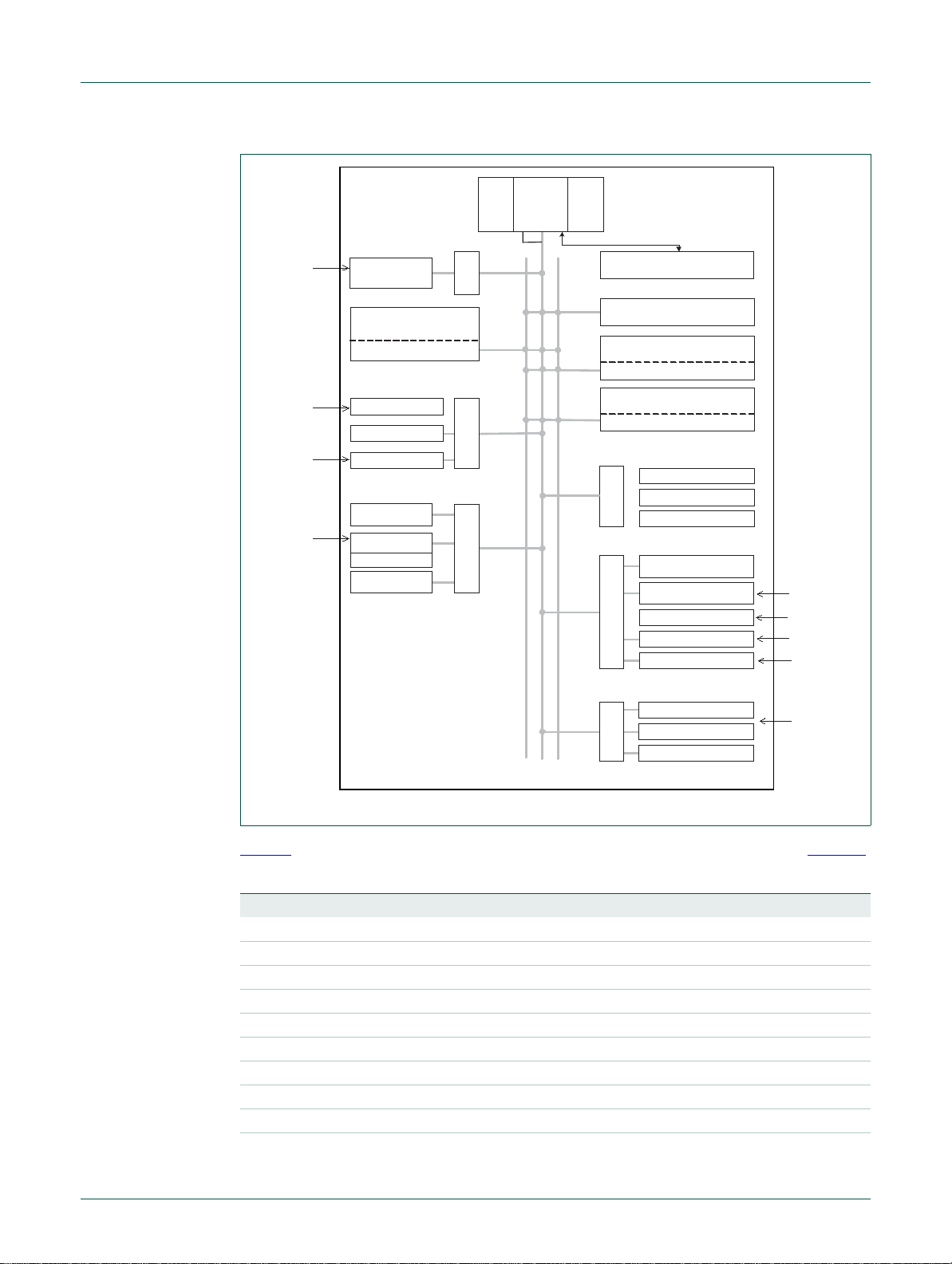
2. Overview
2.1 Functional blocks and clock domains
An overview of the functionality of the LPC2917/19 is given as well as a functional
description of the blocks and their typical usage. Register descriptions are given in the
appropriate sub-sections. The Datasheet Ref. 1
This chapter gives an overview of the functional blocks, clock domains, power modes an d
the interrupt and wake-up structure.
Figure 1 gives a simplified overview of the functional blocks. These blocks are explained
in detail in Section 3
gathered into subsystems and one or more of these blocks and/or subsystems are put into
a clock domain. Each of these clock domains can be configured individually for power
management (i.e. clock on or off and whether the clock responds to sleep and wake-up
events).
(with the exception of some trivial blocks). Several blocks are
should be used along with this document.
UMxxxxx © NXP B.V. 2007. All rights reserved.
User manual Rev. 01.02. — 8 November 2007 3 of 263
Page 4
NXP Semiconductors
General Subsystem
Event Router (ER)
System Control Unit (SCU)
Chip Feature ID (CFID)
AHB2VPB
Bridge
s
IEEE 1149.1 JTAG TEST and
DEBUG INTERFACE
LPC2917/19
DTCM
16 Kb
ITCM
16 Kb
ARM968E-S
m
s
s
s
s
s
s
s
s
s
External Static Memory
Controller (SMC)
Embedded
SRAM Memory 32 Kb
SRAM Controller #0
Embedded
FLASH Memory
512 - 768 Kb
FLASH Memory Controller (FMC)
Embedded
SRAM Memory 16 Kb
SRAM Controller #1
GLOBAL ACCEPTANCE
FILTER
2 Kbyte Static RAM
LIN MASTER 0/1
CAN Controller
0, 1
Vectored Interrupt
Controller (VIC)
AHB2VPB
Bridge
AHB2DTL
Bridge
Modulation and Sampling
Control Subsystem
PWM 0, 1, 2, 3
ADC 1, 2
Timer 0, 1 (MTMR)
AHB2VPB
Bridge
Power Clock Reset
Control Subsystem
Power Management Unit (PMU)
Reset Generation Unit (RGU)
Clock Generation Unit (CGU)
AHB2DTL
Bridge
Peripheral Subsystem
General Purpose IO (GPIO)
0, 1, 2, 3
Timer (TMR)
0, 1, 2, 3
Watchdog Timer (WDT)
UART 0, 1
AHB2VPB
Bridge
TMR_CLK
SAFE_CLK
UART_CLK
SPI_CLK
PCR_CLK
IVNSS_CLK
ADC_CLK
MSCSS_CLK
SYS_CLK
SPI 0, 1, 2
s
DRAFT
Preliminary UM
LPC2917/19 - ARM9 microcontroller with CAN and LIN
D
RAFT DRAFT DRAFT DRAFT DRAFT D
D
RAFT DRA
D
RAFT
DR
AFT
DRAFT
DRA
F
T DRAFT DRAFT DRAFT DRA
DR
AFT
DRAFT
DR
F
T DRAF
UMxxxxx © NXP B.V. 2007. All rights reserved.
User manual Rev. 01.02. — 8 November 2007 4 of 263
Fig 1. LPC2917/19 clock distribution
Table 1 gives an overview of the clock domains and functional blocks, as used in Figure 1.
Table 1. Functional blocks and clock domains
Short Description Comment
Clock domain 0 - AHB
ARM ARM9TDMI-S 32-bit RISC processor
SMC Static Memory Controller For external (static) memory banks
SRAM Internal Static Memory Clock domain 1 – Flash
Flash - Internal Flash Memory
FMC Flash Memory Controller Controller for the internal flash memory
Clock domain 2 – General and Peripheral subsystems
General subsystem
CFID Digital In-vehicle Chip ID Identifies the device and its possibilities
Page 5

NXP Semiconductors
Table 1. Functional blocks and clock domains
Short Description Comment
CGU Clock Generation Unit Controls clock sources and clock
ER Event Router Routes wake-up events and external
RTC Real-Time Clock RTC with own power domain (e.g. for
SCU System Control Unit Configures memory map and I/O
SPI Serial Peripheral Interface Supports various industry-standard SPI
WD Watchdog Timer to guard (software) execution
Peripheral subsystem
GPIO General-Purpose
TMR Timer Provides match output and capture
UART Universal Asynchronous
VIC Vectored Interrupt Controller Prioritized/vectored interrupt handling
Modulation and sampling-control subsystem
ADC Analog-to-Digital Converter 10-bit Analog-to-Digital Converter
PWM Pulse-Width Modulator Synchronized Pulse-Width Modulator
TMR Timer Dedicated Sampling and Control Timer
Clock domain 3 – In-Vehicle Networking subsystem
Remark: There is also a fifth clock domain. This is used by the converter of the ADCs to determine
the conversion rate.
CAN Gateway Includes acceptance filter
LIN Master controller LIN master controller
- - Clock for the converter part of the ADC
DRAFT
Preliminary UM
D
RAFT DRAFT DRAFT DRAFT DRAFT D
D
RAFT DRA
D
LPC2917/19 - ARM9 microcontroller with CAN and LIN
F
T DRAFT DRAFT DRAFT DRA
…continued
domains
interrupts (to CGU/VIC)
battery)
functions
protocols
Directly controls I/O pins
Input/Output
inputs
Standard 550 serial port
Receiver/Transmitter
determining the conversion rate.
RAFT
DRAFT
DR
AFT
DRA
DR
AFT
DRAFT
DR
F
T DRAF
UMxxxxx © NXP B.V. 2007. All rights reserved.
User manual Rev. 01.02. — 8 November 2007 5 of 263
Page 6
NXP Semiconductors
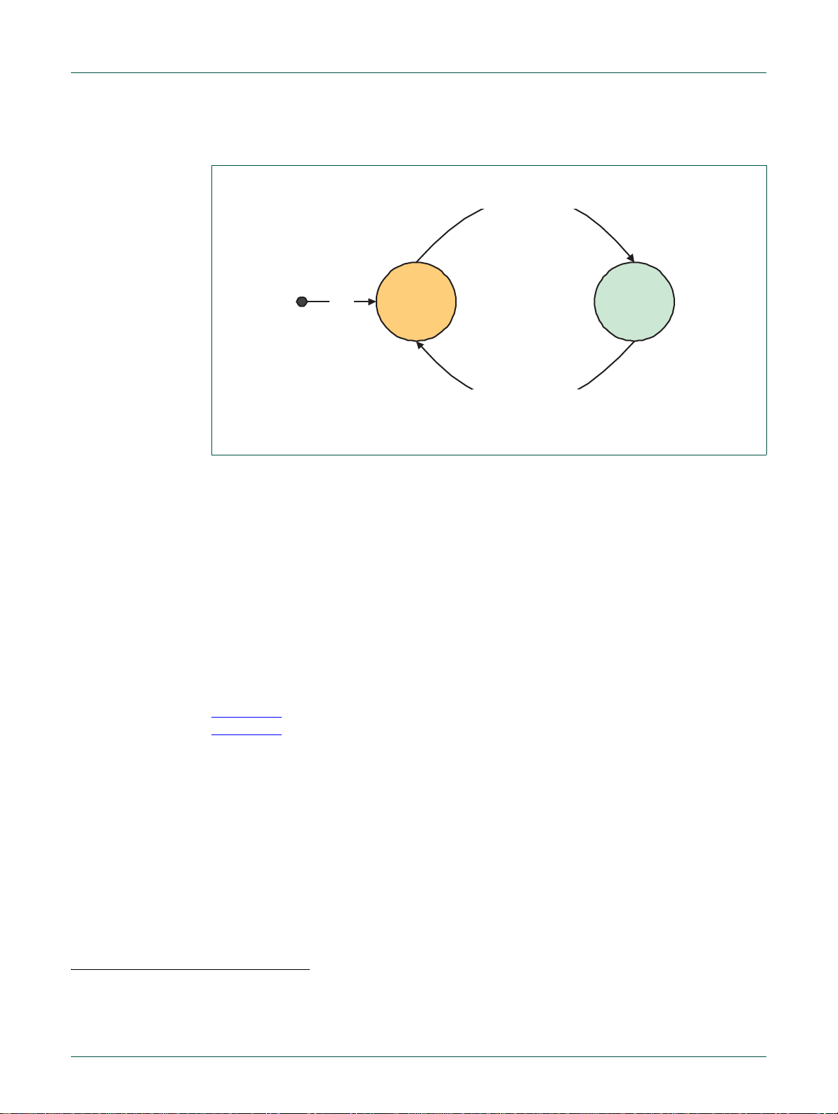
Power Mode
“Normal”
Power Mode
“Idle”
Power Mode := “Idle”
(CGU.CPM register)
wake-up event
(from Event Router to CGU )
Reset
2.2 Power modes
DRAFT
Preliminary UM
LPC2917/19 - ARM9 microcontroller with CAN and LIN
D
RAFT DRAFT DRAFT DRAFT DRAFT D
D
RAFT DRA
D
RAFT
DR
AFT
DRAFT
DRA
F
T DRAFT DRAFT DRAFT DRA
DR
AFT
DRAFT
DR
F
T DRAF
Fig 2. Power modes
The device operates in normal-power mode after reset. In this mode the device is fully
functional, i.e. all clock domains are available
1
. The system can be put into idle-power
mode either partially or fully. In this mode selected clock domains are switched off, and
this might also suspend execution of the software. The clock domains are enabled again
upon a wake-up event. This wake-up event is provided by the Event Router.
The clock domains that can be switched off during idle-power mode depend on the
selected wake-up events. For an external interrupt (e.g. EXTINT0) no active clock is
required, i.e. all clock domains can be switched off. However, for wake-up on a timer
interrupt the clock domain of the timer should stay enabled during low-power mode. In
general, each subsystem that might cause a wake-up upon an interrupt must be excluded
from the low power mode, i.e. the clock domain of the subsystem should stay enabled.
Setting the power mode and configuring the clock domains is handled by the CGU, see
Section 3.3
Section 3.6
. Configuration of wake-up events is handled by the Event Router, see
.
2.3 Memory map
2.3.1 Memory-map view of different AHB master layers
The LPC2917/19 has a multi-layer AHB bus structure with three layers. The different bus
masters in the LPC2917/19 (CPU, FRSS_A and FRSS_B) each have their own AHB-lite
system bus (layer). AHB slaves are hooked up to these AHB-lite busses. Not all slaves
are connected to all layers, so the individual AHB bus masters in the LPC2917/19 each
have their own view of the system memory map.
2
The ARM968E-S CPU has access to all AHB slaves and hence to all address regions.
1. Although all clock domains are available, not all the domains are enabled. E.g. the ADC clock domain is switched off by default
after reset.
2. The CAN and LIN controllers can issue a wake-up event via activity on the CAN or LIN bus. This feature does not require an active
clock for their subsystem; but the first message can be lost.
UMxxxxx © NXP B.V. 2007. All rights reserved.
User manual Rev. 01.02. — 8 November 2007 6 of 263
Page 7

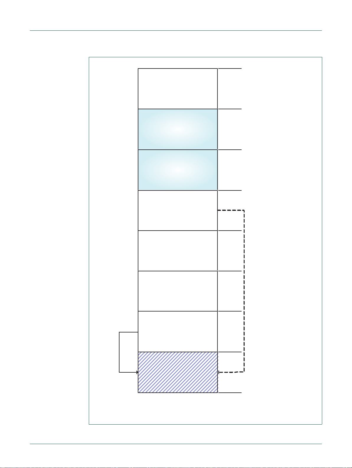
NXP Semiconductors
2.3.2 Memory-map regions
The ARM9 processor has a 4 GB of address space. The LPC2917/19 has divided this
memory space into eight regions of 512 MB each. Each region is used for a dedicated
purpose.
DRAFT
Preliminary UM
LPC2917/19 - ARM9 microcontroller with CAN and LIN
D
RAFT DRAFT DRAFT DRAFT DRAFT D
D
RAFT DRA
D
RAFT
F
T DRAFT DRAFT DRAFT DRA
DR
AFT
DRAFT
DRA
DR
AFT
DRAFT
DR
F
T DRAF
Figure 3
gives a graphical overview of the LPC2917/19 memory map.
UMxxxxx © NXP B.V. 2007. All rights reserved.
User manual Rev. 01.02. — 8 November 2007 7 of 263
Page 8
NXP Semiconductors
DRAFT
Preliminary UM
D
RAFT DRAFT DRAFT DRAFT DRAFT D
D
RAFT DRA
D
RAFT
LPC2917/19 - ARM9 microcontroller with CAN and LIN
F
T DRAFT DRAFT DRAFT DRA
0xFFFF_FFFF
Region #7 (512 Mbyte)
Bus Peripherals
0xE000_0000
Region #6 (512 Mbyte)
(reserved for future extensions)
0xC000_0000
Region #5 (512 Mbyte)
(reserved for future extensions)
DR
AFT
DRAFT
DRA
DR
AFT
DRAFT
DR
F
T DRAF
Embedded
flash
remapped
during
start-up
Region #4 (512 Mbyte)
embedded SRAM
Region #3 (512 Mbyte)
Static Memory Controller / External Bus Interface
(Configuration Area)
Region #2 (512 Mbyte)
Static Memory Controller / External Bus Interface
(Data Transfer Area)
Region #1 (512 Mbyte)
embedded FLASH
Region #0 (512 Mbyte)
Reserved for TCM
0xA000_0000
0x8000_0000
0x6000_0000
0x4000_0000
0x2000_0000
Programmable selection of remap
area via register in SCU
(example: embedded SRAM)
0x0000_0000
System Memory Map
(Memory Regions)
Fig 3. AHB system memory map: graphical overview
UMxxxxx © NXP B.V. 2007. All rights reserved.
User manual Rev. 01.02. — 8 November 2007 8 of 263
Page 9
NXP Semiconductors
Region #0: TCM area
0x0000_0000 - 0x1FFF_FFFF
(Offset Address)
0x0000_0000
0x1FFF_FFFF
0x0000_4000
0x0040_0000
I-TCM region aliasses
I-TCM (16 kByte)
0x0080_0000
D-TCM region aliasses
D-TCM (16 kByte)
region #0 no physical memory
0x0040_4000
2.3.2.1 Region 0: TCM area
The ARM968E-S processor has its exception vectors located at address logic 0. Since
flash is the only non-volatile memory available in the LPC2917/19, the exception vectors
in the flash must be located at address logic 0 at reset (AHB_RST).
After booting a choice must be made for region 0. When enabled the Tightly Coupled
Memories (TCMs) occupy fixed address locations in region 0 as indicated in Figure 4
Information on how to enable the TCMs can be found in the ARM documentation, see
Ref. 2
DRAFT
Preliminary UM
LPC2917/19 - ARM9 microcontroller with CAN and LIN
D
RAFT DRAFT DRAFT DRAFT DRAFT D
D
RAFT DRA
D
RAFT
DR
DRAFT
F
T DRAFT DRAFT DRAFT DRA
AFT
DRA
DR
AFT
DRAFT
DR
F
T DRAF
.
.
UMxxxxx © NXP B.V. 2007. All rights reserved.
User manual Rev. 01.02. — 8 November 2007 9 of 263
Fig 4. Region 0: TCM memory
2.3.2.2 Region 1: embedded flash area
Figure 5
gives a graphical overview of the embedded flash memory map.
Page 10

NXP Semiconductors
0x00000000
0x1FFFFFFF
0x00200000
FLASH IF1
Configuration Area (4 Kbyte)
0x00200FFF
Embedded FLASH
memory area
512 Kbyte -
768 Kbyte
0x0007FFFF - 0x000BFFFF
DRAFT
Preliminary UM
LPC2917/19 - ARM9 microcontroller with CAN and LIN
D
RAFT DRAFT DRAFT DRAFT DRAFT D
D
RAFT DRA
D
RAFT
DR
AFT
DRAFT
DRA
F
T DRAFT DRAFT DRAFT DRA
DR
AFT
DRAFT
DR
F
T DRAF
Fig 5. Region 1 embedded flash memory
Region 1 is reserved for the embedded flash. A data area of 2 Mbyte (to be prepared for a
larger flash-memory instance) and a configuration area of 4 kB are reserved for each
embedded flash instance. Although the LPC2917/19 contains only one embedded flash
instance, the memory aperture per instance is defined at 4 Mbyte.
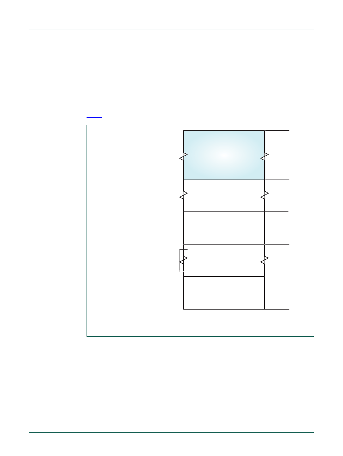
2.3.2.3 Region 2: external static memory area
Region 2 is reserved for the external static memory. The LPC2917/19 provides I/O pi ns for
eight bank-select signals and 24 address lines. This implies that eight memory banks of
16 Mbytes each can be addressed externally.
2.3.2.4 Region 3: external static memory controller area
The external Static-Memory Controller configuration area is located at region 3
2.3.2.5 Region 4: internal SRAM area
Figure 6
gives a graphical overview of the internal SRAM memory map.
UMxxxxx © NXP B.V. 2007. All rights reserved.
User manual Rev. 01.02. — 8 November 2007 10 of 263
Page 11

NXP Semiconductors
Region #4: embedded SRAM
0x8000_0000 - 0x9FFF_FFFF
DRAFT
Preliminary UM
LPC2917/19 - ARM9 microcontroller with CAN and LIN
embedded Memory (Controller) #2..#N
Data Transfer Area
(reserved for future extensions)
D
RAFT DRAFT DRAFT DRAFT DRAFT D
D
RAFT DRA
D
RAFT
DR
AFT
DRAFT
DRA
F
T DRAFT DRAFT DRAFT DRA
0x1FFF_FFFF
DR
AFT
DRAFT
DR
F
T DRAF
Fig 6. Region 4 internal SRAM memory
Region 4 is reserved for internal SRAM. The LPC2917/19 has two internal SRAM
instances. Instance #0 is 32 kB, instance #1 is 16 kB. See Section 3.5.2.3
2.3.2.6 Region 5
Not used.
2.3.2.7 Region 6
Not used.
2.3.2.8 Region 7: bus-peripherals area
Figure 7
gives a graphical overview of the bus-peripherals area memory map.
embedded Memory (Controller) #1
Data Transfer Area (16kByte)
embedded Memory (Controller) #0
Data Transfer Area (32kByte)
0x0000_c000
0x000_8000
0x0000_0000
(Offset Address)
UMxxxxx © NXP B.V. 2007. All rights reserved.
User manual Rev. 01.02. — 8 November 2007 11 of 263
Page 12

NXP Semiconductors
DRAFT
Preliminary UM
LPC2917/19 - ARM9 microcontroller with CAN and LIN
D
RAFT DRAFT DRAFT DRAFT DRAFT D
D
RAFT DRA
D
RAFT
DR
AFT
DRAFT
DRA
F
T DRAFT DRAFT DRAFT DRA
DR
AFT
DRAFT
DR
F
T DRAF
Interrupt Controller (4 kByte)
VIC
Not Used
Power, Clock & Reset Area (12 kByte)
Reserved for future FRSS extensions
PCR
Reserved
MMIO Area
(reserved for future extensions)
0x1FFF_FFFF
0x1FFF_F000
0x1FFF_B000
0x1FFF_8000
0x1FFF_7000
0x1FFF_6000
Region #7: Bus Peripherals
0xE000_0000 - 0xFFFF_FFFF
Peripheral Cluster #7..#N
(reserved for future extensions)
Peripheral Cluster #6 (128 kByte)
MSCSS
Peripheral Cluster #5 (128 kByte)
(reserved for future extensions)
Peripheral Cluster #4 (128 kByte)
IVNSS
Peripheral Cluster #3 (128 kByte)
(reserved for future extensions)
Peripheral Cluster #2 (128 kByte)
PeSS
Peripheral Cluster #1 (128 kByte)
(reserved for future extensions)
Peripheral Cluster #0 (128 kByte)
GeSS
0x1000_0000
0x000E_0000
0x000C_0000
0x000A_0000
0x0008_0000
0x0006_0000
0x0004_0000
0x0002_0000
0x0000_0000
(Offset Address)
Fig 7. Region 7 bus-peripherals area memory
Region 7 is reserved for all stand-alone memory-mapped bus peripherals.
UMxxxxx © NXP B.V. 2007. All rights reserved.
User manual Rev. 01.02. — 8 November 2007 12 of 263
Page 13

NXP Semiconductors
The lower part of region 7 is again divided into VPB clusters, also referred to as
subsystems in this User Manual. A VPB cluster is typically used as the address space for
a set of VPB peripherals connected to a single AHB2VPB bridge, the slave on the AHB
system bus. The clusters are aligned on 256 kB boundaries. In the LPC2917/19 four VPB
clusters are in use: General SubSystem (GeSS), Peripheral SubSystem (PeSS), InVehicle Networking SubSystem (IVNSS) and the Modulation and Sampling SubSystem
(MSCSS). The VPB peripherals are aligned on 4 kB boundaries inside the VPB clusters.
The upper part of region 7 is used as the memory area where memory-mapped register
interfaces of stand-alone AHB peripherals and a DTL cluster reside. Each of these is a
slave on the AHB system bus. In the LPC2917/19 two such slaves are present: the Power,
Clock and Reset subsystem (PCRSS) and the Vectored Interrupt Controller (VIC). The
PCRSS is a DTL cluster in which the CGU, PMU and RGU are connected to the AHB
system bus via an AHB2DTL adapter. The VIC is a DTL target connected to the AHB
system bus via its own AHB2DTL adapter.
2.3.3 Memory-map operating concepts
DRAFT
Preliminary UM
LPC2917/19 - ARM9 microcontroller with CAN and LIN
D
RAFT DRAFT DRAFT DRAFT DRAFT D
D
RAFT DRA
D
RAFT
F
T DRAFT DRAFT DRAFT DRA
DR
AFT
DRAFT
DRA
DR
AFT
DRAFT
DR
F
T DRAF
The basic concept in the LPC2917/19 is that each memory area has a ‘natural’ location in
the memory map. This is the address range for which code residing in that area is written.
Each memory space remains permanently fixed in the same location, eliminatin g the need
to have portions of the code designed to run in different address ran ges.
Because of the location of the exception-handler vectors on the ARM9 processor (at
addresses 0000 0000h through 0000 001Ch: see Table 2
embedded flash is mapped at address 0000 0000h to allow initial code to be executed
and to perform the required initialization, which starts executing at 0000 0000h.
The LPC2917/19 generates the appropriate bus-cycle abort exception if an access is
attempted for an address that is in a reserved or unused address region or unassigned
peripheral spaces. For these areas bo th attempted data accesses and instruction fetches
generate an exception. Note that write-access addresses should be word-aligned in ARM
code or half-word aligned in Thumb code. Byte-aligned writes are performed as word or
half-word aligned writes without error signalling.
Within the address space of an existing peripheral a dat a-abort exception is not gener ated
in response to an access to an undefined address. Address decoding within each
peripheral is limited to that needed to distinguish defined registers within the peripheral
itself. Details of address aliasing within a peripheral space are not defined in the
LPC2917/19 documentation and are not a supported feature.
Note that the ARM stores the pre-fetch abort flag along with the associated instruction
(which will be meaningless) in the pipeline and processes the abort only if an attempt is
made to execute the instruction fetched from the illegal address. This prevents the
accidental aborts that could be caused by pre-fetches occurring when code is executed
very near to a memory boundary.
) By default, after reset, the
Table 3
UMxxxxx © NXP B.V. 2007. All rights reserved.
User manual Rev. 01.02. — 8 November 2007 13 of 263
gives the base-address overview of all peripherals:
Page 14

NXP Semiconductors
Table 2. Interrupt vectors address table
Address Exception
0000 0000h Reset
0000 0004h Undefined instruction
0000 0008h Software interrupt
0000 000Ch Pre-fetch abort (instruction-fetch memory fault)
0000 0010h Data abort (data-access memory fault)
0000 0014h reserved
0000 0018h IRQ
0000 001Ch FIQ
Table 3. Peripherals base-address overview
Base address Base name AHB peripherals
Memory region 0 to region 6
0000 0000h TCM memory
2000 0000h Embedded flash memory
2020 0000h FMC RegBase Embedded-flash controller
4000 0000h External static memory
6000 0000h SMC RegBase External Static-Memory Controller
8000 0000h Internal SRAM memory
VPB Cluster 0: general subsystem
E000 0000h CFID RegBase Chip/feature ID register
E000 1000h SCU RegBase System Control Unit
E000 2000h ER RegBase Event Router
VPB Cluster 2: peripheral subsystem
E004 0000h WDT RegBase Watchdog Timer
E004 1000h TMR RegBase Timer 0
E004 2000h TMR RegBase Timer 1
E004 3000h TMR RegBase Timer 2
E004 4000h TMR RegBase Timer 3
E004 5000h UART RegBase 16C550 UART 0
E004 6000h UART RegBase 16C550 UART 1
E004 7000h SPI RegBase SPI 0
E004 8000h SPI RegBase SPI 1
E004 9000h SPI RegBase SPI 2
E004 A000h GPIO RegBase General-Purpose I/O 0
E004 B000h GPIO RegBase General-Purpose I/O 1
E004 C000h GPIO RegBase General-Purpose I/O 2
E004 D000h GPIO RegBase General-Purpose I/O 3
VPB Cluster 4:
E008 0000h CANC RegBase CAN controller 0
DRAFT
Preliminary UM
LPC2917/19 - ARM9 microcontroller with CAN and LIN
configuration registers
configuration registers
D
RAFT DRAFT DRAFT DRAFT DRAFT D
D
RAFT DRA
D
RAFT
DR
AFT
DRAFT
DRA
F
T DRAFT DRAFT DRAFT DRA
DR
AFT
DRAFT
DR
F
T DRAF
UMxxxxx © NXP B.V. 2007. All rights reserved.
User manual Rev. 01.02. — 8 November 2007 14 of 263
Page 15

NXP Semiconductors
Table 3. Peripherals base-address overview
Base address Base name AHB peripherals
E008 1000h CANC RegBase CAN controller 1
E008 6000h CANAFM RegBase CAN ID look-up table memory
E008 7000h CANAFR RegBase CAN acceptance filter registers
E008 8000h CANCS RegBase CAN central status registers
E008 9000h LIN RegBase LIN master controller 0
E008 A000h LIN RegBase LIN master controller 1
VPB Cluster 6: modulation and sampling-control subsystem
E00C 0000h MTMR RegBase MSCSS timer 0
E00C 1000h MTMR RegBase MSCSS timer 1
E00C 3000h ADC RegBase ADC 1
E00C 4000h ADC RegBase ADC 2
E00C 5000h PWM RegBase PWM 0
E00C 6000h PWM RegBase PWM 1
E00C 7000h PWM RegBase PWM 2
E00C 8000h PWM RegBase PWM 3
Power, Clock and Reset control cluster
FFFF 8000h CGU RegBase Clock Generation Unit
FFFF 9000h RGU RegBase Reset Generation Unit
FFFF A000h PMU RegBase Power Management Unit
Vector interrupt controller
FFFF F000h VIC RegBase Vectored Interrupt Controller
DRAFT
Preliminary UM
LPC2917/19 - ARM9 microcontroller with CAN and LIN
…continued
D
RAFT DRAFT DRAFT DRAFT DRAFT D
D
RAFT DRA
D
RAFT
DR
AFT
DRAFT
DRA
F
T DRAFT DRAFT DRAFT DRA
DR
AFT
DRAFT
DR
F
T DRAF
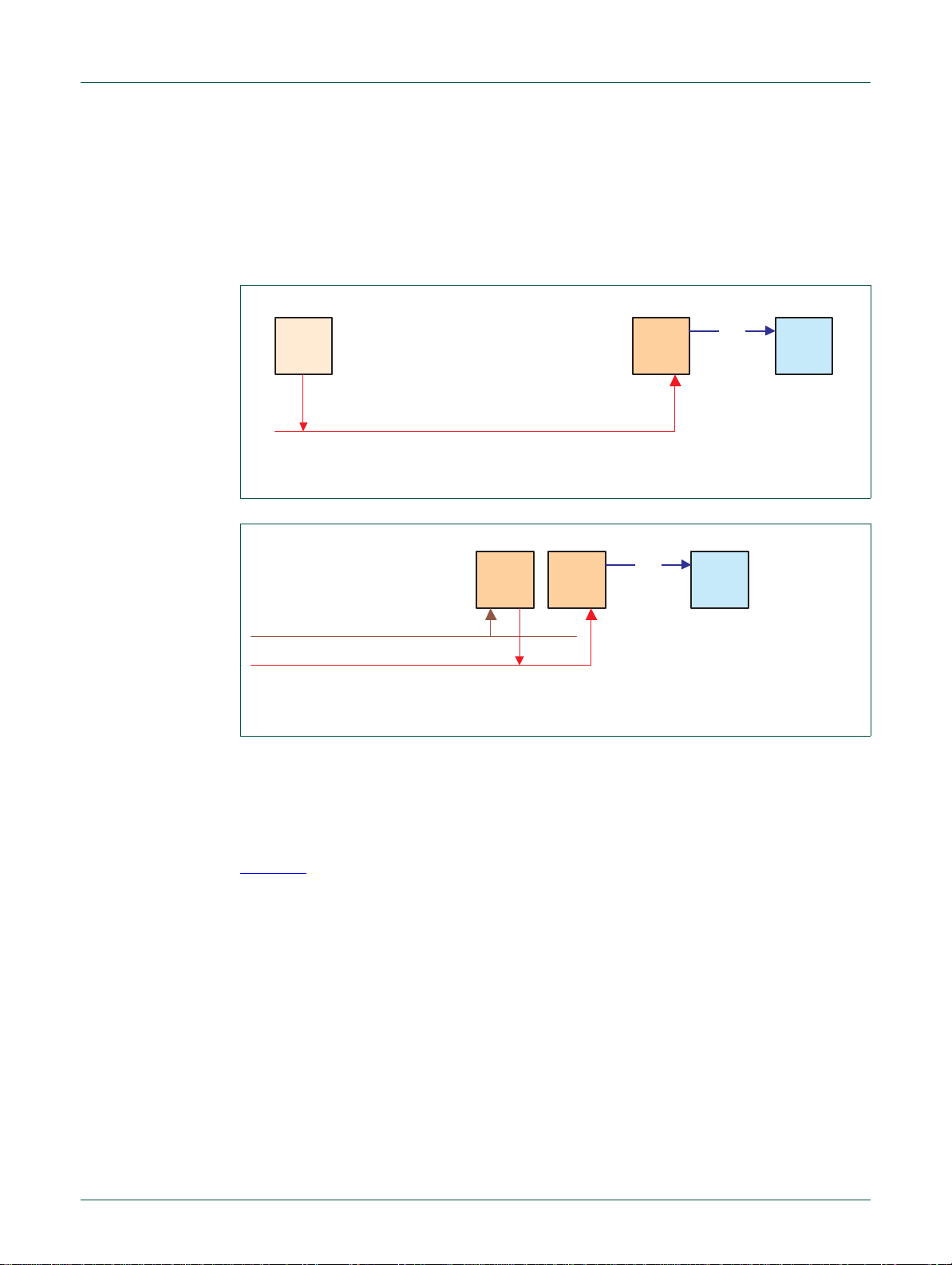
2.4 Interrupt and wake-up structure
An overview of the interrupt and wake-up structure is given in Figure 8. The main
functions are:
• Events and interrupt requests causing an interrupt (IRQ or FIQ) on the ARM
processor.
• Events and interrupt requests causing a wake-up. During low-power mode selected
clock domains are switched off, and they are turned on by this wake-up.
wake-up
R
I
Ext.
Int.
UART
...
...
...
RTC
Interrupt Requests
CGU VIC ARM
Events
Event
Router
Fig 8. Interrupt and wake-up structure
UMxxxxx © NXP B.V. 2007. All rights reserved.
User manual Rev. 01.02. — 8 November 2007 15 of 263
Q
FIQ
Page 16
NXP Semiconductors
VIC ARM
IRQ
UART
Interrupt Requests
Event
Router
VIC ARM
IRQ
Interrupt Requests
Events
In this case the VIC (Vectored Interru pt Controller) is configured to send an interr upt (IRQ
or FIQ) towards the ARM processor. Examples are interrupts to indicate the reception of
data via a serial interface, or timer interrupts. The Event Router serves as a multiplexer for
internal and external events (e.g. RTC tick and external interrupt lines) and indicates the
occurrence of such an event towards the VIC (Event-Router interrupt). The Event Router
is also able to latch the occurrence of these events (level or edge-triggered).
Fig 9. Interrupt (UART) causing an IRQ
DRAFT
Preliminary UM
LPC2917/19 - ARM9 microcontroller with CAN and LIN
D
RAFT DRAFT DRAFT DRAFT DRAFT D
D
RAFT DRA
D
RAFT
DR
AFT
DRAFT
DRA
F
T DRAFT DRAFT DRAFT DRA
DR
AFT
DRAFT
DR
F
T DRAF
Fig 10. Event causing an IRQ
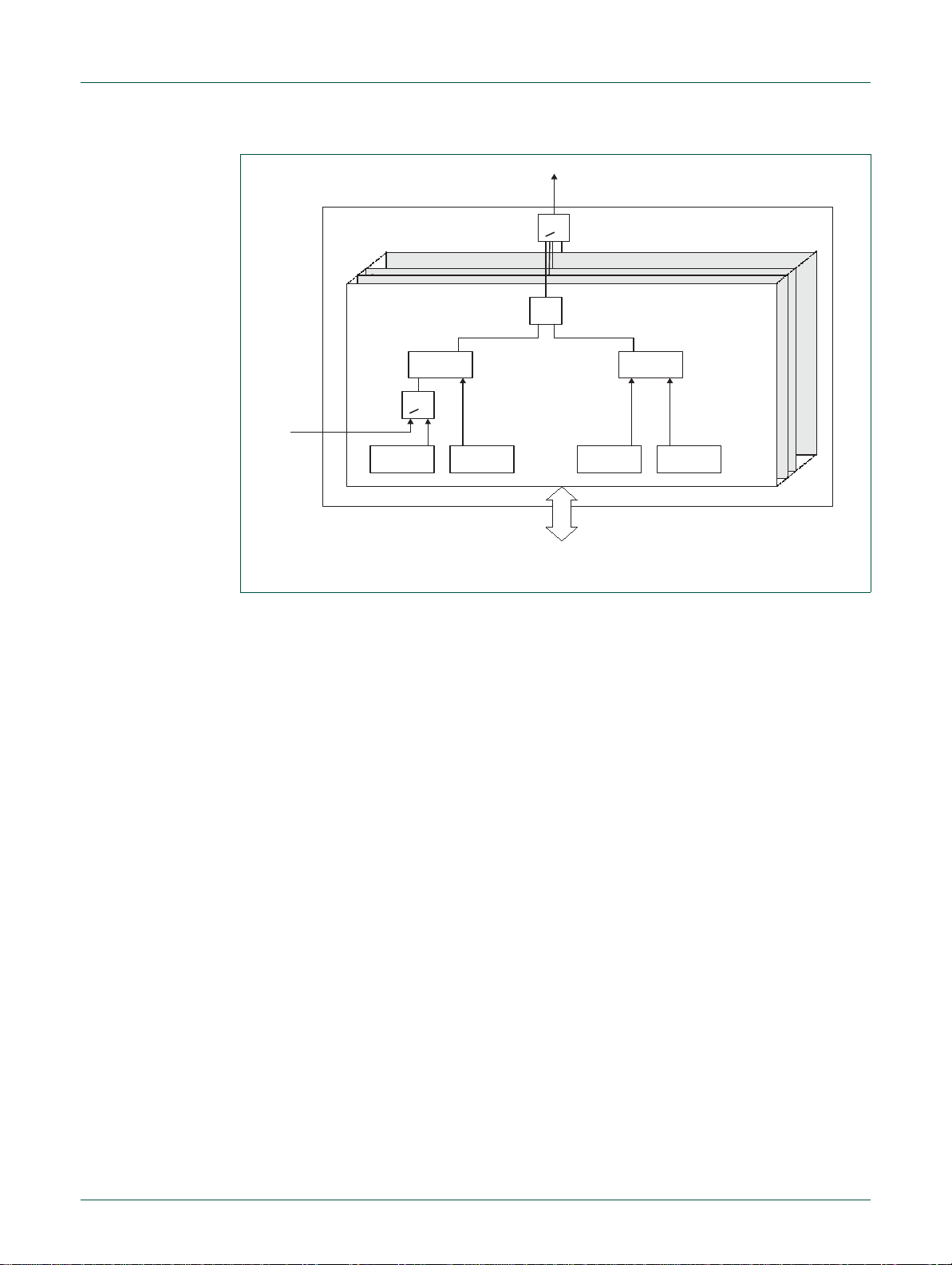
2.4.1 Interrupt device architecture
In the LPC2917/19 a general approach is taken to generate inter rupt requests towards the
CPU. A vectored Interrupt Controller (VIC) receives and collects the interrupt requests as
generated by the several modules in the device.
Figure 11
the parameters provided by the user software.
shows the logic used to gate the event signal originating from the function with
UMxxxxx © NXP B.V. 2007. All rights reserved.
User manual Rev. 01.02. — 8 November 2007 16 of 263
Page 17
NXP Semiconductors
31
2
1
0
STATUS
&
SET
STATUS
CLEAR
STATUS
ENABLE
SET
ENABLE
CLEAR
ENABLE
>1
>1
Event
Interrupt
Request
Control
Interface
DRAFT
Preliminary UM
LPC2917/19 - ARM9 microcontroller with CAN and LIN
D
RAFT DRAFT DRAFT DRAFT DRAFT D
D
RAFT DRA
D
RAFT
DR
AFT
DRAFT
DRA
F
T DRAFT DRAFT DRAFT DRA
DR
AFT
DRAFT
DR
F
T DRAF
Fig 11. I nterrupt device architecture
A set of software-accessible variables is provided for each interrupt source to control and
observe interrupt request generation. In general, a pair of read-only registers is used for
each event that leads to an interrupt request:
• STATUS captures the event. The variable is typically set by a hardware event and
cleared by the software ISR, but for test purposes it can also be set by software
• ENABLE enables the assertion of an interrupt-request output signal for the captured
event
In conjunction with the STATUS/ENABLE variables, commands are provided to set and
clear the variable state through a software write-action to write-only registers. These
commands are SET_STATUS, CLR_STATUS, SET_ENABLE and CLR_ENABLE.
The event signal is logically OR-ed with its associated SET_STATUS register bit, so both
events writing to the SET_STATUS register sets the STATUS register.
Typically, the result of multiple STATUS/ENABLE pairs is logically OR-ed per functional
group, forming an interrupt request signal towards the Vectored Interrupt Controller.
2.4.2 Interrupt registers
A list is provided for each function in the detailed block-description part of this document,
containing the interrupt sources for that function. A table is also provide d to indicate the bit
positions per interrupt source. These positions are identical for all the six registers
INT_STATUS, INT_ENABLE, INT_SET_STATUS, INT_CLEAR_STATUS,
INT_SET_ENABLE and INT_CLEAR_ENABLE.
UMxxxxx © NXP B.V. 2007. All rights reserved.
User manual Rev. 01.02. — 8 November 2007 17 of 263
Up to 32 interrupt bits are available for each register .
Page 18

NXP Semiconductors
2.4.2.1 Interrupt clear-enable register
Write ‘1’ actions to this register set one or more ENABLE variables in the INT_ENABLE
register. INT_SET_ENABLE is write-only. Writing a 0 has no effect.
Table 4. INT_CLR_ENABLE register bit description
Bit Variable Name Access Value Description
i CLR_ENABLE[i] W 1 Clears the ENABLE[i] variable in corresponding
2.4.2.2 Interrupt set-enable register
Write ‘1’ actions to this register set one or more ENABLE variables in the INT_ENABLE
register. INT_SET_ENABLE is write-only. Writing a 0 has no effect.
Table 5. INT_SET_ENABLE register bit description
Bit Variable Name Access Value Description
i SET_ENABLE[i] W 1 Sets the ENABLE[i] variable in corresponding
DRAFT
Preliminary UM
LPC2917/19 - ARM9 microcontroller with CAN and LIN
INT_ENABLE register (set to 0)
INT_ENABLE register to 1
D
RAFT DRAFT DRAFT DRAFT DRAFT D
D
RAFT DRA
D
RAFT
DR
AFT
DRAFT
DRA
F
T DRAFT DRAFT DRAFT DRA
DR
AFT
DRAFT
DR
F
T DRAF
2.4.2.3 Interrupt status register
The interrupt status register reflects the status of the corresponding interrupt event that
leads to an interrupt request. INT_STATUS is a read-only register. Its content is either
changed by a hardware event (from logic 0 to 1 in the case of an event), or by software
writing a 1 to the INT_CLR_STATUS or INT_SET_STATUS register.
T able 6. INT_STATUS register bit description
* = reset value
Bit Variable Name Access Value Description
i STATUS[i] R 1 Event captured; request for interrupt service on
2.4.2.4 Interrupt enable register
This register enables or disables generation of inte rrupt requests on associated interruptrequest output signals. INT_ENABLE is a read-only register. Its content is changed by
software writing to the INT_CLR_ENABLE or INT_SET_ENABLE registers.
Table 7. INT_ENABLE register bit description
* = reset value
Bit Variable Name Access Value Description
i ENABLE[i] R 1 Enables interrupt request generation. The
the corresponding interrupt request signal if
ENABLE[i] = 1 interrupt for end of scan
0*
corresponding interrupt request output signal is
asserted when STATUS[i] =1
0*
2.4.2.5 Interrupt clear-status register
Write ‘1’ actions to this register clear one or more status variables in the INT_STATUS
register. Writing a ‘0’ has no effect.
UMxxxxx © NXP B.V. 2007. All rights reserved.
User manual Rev. 01.02. — 8 November 2007 18 of 263
Page 19
NXP Semiconductors
T able 8. INT_CLR_STATUS register bit description
Bit Variable Name Access Value Description
i CLR_STATUS[i] W 1 Clears STATUS[i] variable in INT_STATUS
2.4.2.6 Interrupt set-status register
Write ‘1’ actions to this register set one or more STATUS variables in the INT_STATUS
register. This registe r is write-only and is intended for debug purposes. W riting a ‘0’ has no
effect.
Table 9. INT_SET_STATUS register bit description
Bit Variable Name Access Value Description
i SET_STATUS[i] W 1 Sets STATUS[i] variable in INT_STATUS
2.4.3 Wake-up
DRAFT
Preliminary UM
LPC2917/19 - ARM9 microcontroller with CAN and LIN
register (set to 0)
register to 1
D
RAFT DRAFT DRAFT DRAFT DRAFT D
D
RAFT DRA
D
RAFT
DR
AFT
DRAFT
DRA
F
T DRAFT DRAFT DRAFT DRA
DR
AFT
DRAFT
DR
F
T DRAF
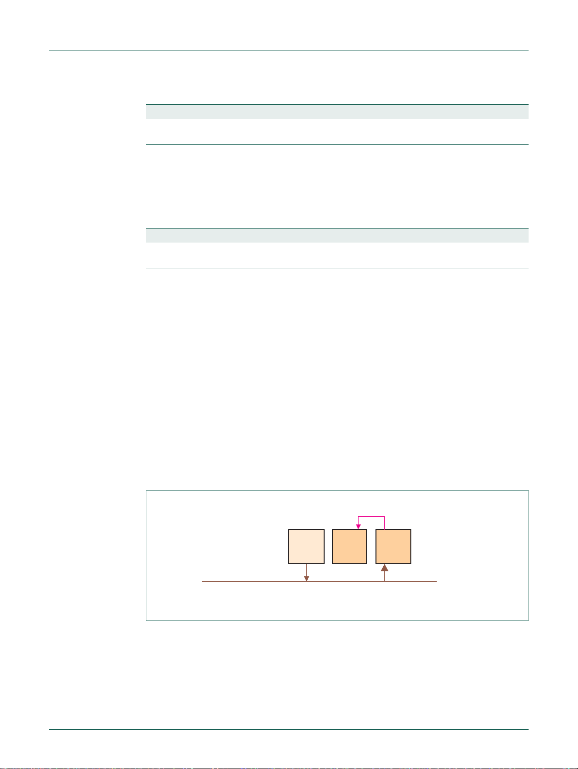
In low-power mode, selected idle clock domains are switched off. The wake-up signal
towards the CGU enables the clock of these domains. A typical application is to configu re
all clock domains to switch off. Since the clock of the ARM processor is also switched off,
execution of software is suspended and resumed on wake-up.
In this case the Event Router is configured to send a wake-up signal towards the CGU
(Clock Generation Unit). Examples are events to indicate the reception of dat a (e.g. on the
CAN receiver) or external interrupts.
The VIC can be used (IRQ wake-up event or FIQ wake-up event of the Event Router) to
generate a wake-up event on an interrupt occurrence. This is only possible if the clock
domain of the interrupt source is excluded from low-power mode. The VIC does not need
a clock to generate these wake-up events.
Examples of use are to configure a timer to wake up the system af ter a defined time, or to
wake up on receiving data via the UART.
wake-up
CGUUART
Event
Router
Events
Fig 12. Interrupt (UART) causing a wake-up
UMxxxxx © NXP B.V. 2007. All rights reserved.
User manual Rev. 01.02. — 8 November 2007 19 of 263
Page 20

NXP Semiconductors
Event
Router
CGU VICUART
wake-up
Interrupt Requests
Events
ARM FMC
Flash
JTAG
interface
(Flash Mode)
JTAG
interface
(ARM mode)
Fig 13. Event (RTC) causing a wake-up
3. Block description
This chapter describes each block and how it is used in a typical application. It is assumed
that the provided drivers Ref. 7
DRAFT
Preliminary UM
LPC2917/19 - ARM9 microcontroller with CAN and LIN
D
RAFT DRAFT DRAFT DRAFT DRAFT D
D
RAFT DRA
D
RAFT
DR
AFT
DRAFT
DRA
F
T DRAFT DRAFT DRAFT DRA
are used.
DR
AFT
DRAFT
DR
F
T DRAF
3.1 Flash Memory Controller (FMC)
3.1.1 Flash Memory Controller functional description
Fig 14. Schema t ic representation of the FMC
The flash memory consists of the embedded flash memory (flash) and a contro ller (the
FMC) to control access to it. The controller can be accessed in two ways: either by
register access in software, running on the ARM core, or directly via the JTAG interface
Figure 14
In the following sections access to the Flash Memory Controller via software is described.
Access via the JTAG interface is described in Section 6
.
.
3.1.2 Flash memory layout
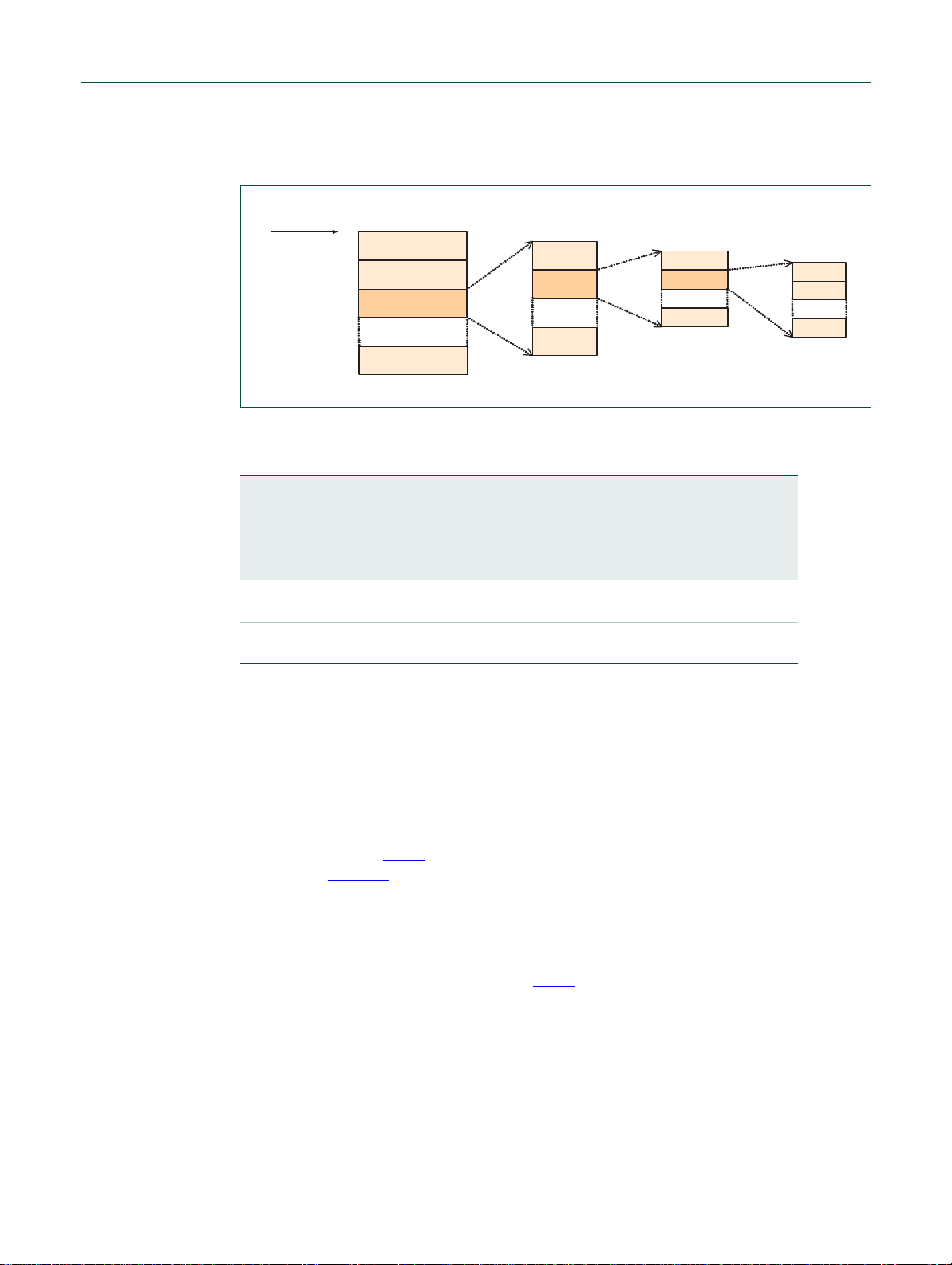
The flash memory is arranged into sectors, pages and flash-words Figure 15. For writing
(erase/burn) the following issues are relevant:
• Protection against erase/burn is arranged per sector.
• Erasing is done per sector.
• Burning - the actual write into flash memory - is done per page.
UMxxxxx © NXP B.V. 2007. All rights reserved.
User manual Rev. 01.02. — 8 November 2007 20 of 263
Page 21
NXP Semiconductors
Base Address of
Flash Memory
Sector 0
Sector 2
Sector 1
Sector s
Page 1
Page 0
Page p
FlashWord 0
FlashWord 1
FlashWord
Byte 0
Byte 1
Byte 15
• The smallest part that can be written at once is a flash-word (16 bytes).
Fig 15. Flash memory layout
Table 10 lists the various parameters of the flash memory.
Table 10. Flash memory layout
Type number Flash size Sector Page
LPC2919 768k 8/11 8192/6553616/128 512 bytes 32 16 byte
DRAFT
Preliminary UM
D
RAFT DRAFT DRAFT DRAFT DRAFT D
D
RAFT DRA
D
RAFT
DR
DRAFT
LPC2917/19 - ARM9 microcontroller with CAN and LIN
F
T DRAFT DRAFT DRAFT DRA
Flash-word
#
small
large
Size
small
large
(per sector)
#
Size # Size
small
large
(per page)
AFT
DRA
DR
AFT
DRAFT
DR
F
T DRAF
LPC2917 512k 8/7 8192/6553616/128 512 byte 32 16 byte
3.1.3 Flash memory reading
During a read (e.g. read-only data or program execu tio n ) no spec ial ac tion s ar e re qu ire d .
The address space of flash memory can simply be accessed like normal ROM with word,
half-word or byte access. It is possible however to modify or optimize the read settings of
the flash memory.
For optimal read performance the flash memory cont ains two intern al 128- bit buf f ers. The
configuration of these buffers and the number of wait-states for unbuffered reads can be
set in the FMC, see Ref. 1
register see Table 18
. For a detailed description of the flash bridge wait-states
.
3.1.4 Flash memory writing
Writing can be split into two parts, erasing and burning. Both operations are
asynchronous; i.e. after initiating the operation it takes some time to complete. Erasing is
a relatively time-consuming process, see Ref. 1
flash memory results in wait-states. To serve interrupts or perform other actions this
critical code must be present outside the flash memory (e.g. internal RAM). Th e code that
initiates the erase/burn operation mus t al so be present outside the flash memory.
Normally the sectors are protected against write actions. Before a write is started the
corresponding sector(s) must be unprotected, after which protection can be enabled
again. Protection is automatically enabled on a reset. During a write (erase/burn)
UMxxxxx © NXP B.V. 2007. All rights reserved.
User manual Rev. 01.02. — 8 November 2007 21 of 263
operation the internal clock of the flash must be enabled. After comp letion the clock can
be disabled again.
. During this process any access to the
Page 22

NXP Semiconductors
In the following sections the typical write (erase and burn) sequences are listed.
3.1.4.1 Erase sequence (for one or more sectors)
• Unprotect sector(s) to be erased.
• Mark sector(s) to be erased.
• Initiate the erase process.
• Wait until erasing is finished see Section 2.4.1.
• Protect sector(s) (optional).
Remark: During the erase process the internal clock of the flash module must be enabled.
3.1.4.2 Burn sequence (for one or more pages)
Burning data into the flash memory is a two-stage process. First the data for a page is
written into data latches, and afterwards the contents of these data latc he s (sin g le page)
are burned into memory. If only a part of a page has to be burned the contents of the data
latches must be preset with logical 1s to avoid changing the remainder of the page.
Presetting these latches is done via the FMC (see Section 3.1.7
DRAFT
Preliminary UM
LPC2917/19 - ARM9 microcontroller with CAN and LIN
D
RAFT DRAFT DRAFT DRAFT DRAFT D
D
RAFT DRA
).
D
RAFT
F
T DRAFT DRAFT DRAFT DRA
DR
AFT
DRAFT
DRA
DR
AFT
DRAFT
DR
F
T DRAF
• Unprotect the sectors containing the pa ges to be burned.
• For each page:
– Preset the data latches of the flash module (only required if a part of a page has to
be programmed; otherwise optional).
– Write data for the page into the data latches (ordin ary 32-bit word writes to the
address space of the flash memory).
Remark: Data must be written from flash-word boun daries onwards and must be a
multiple of a flash-word.
– Initiate the burn process.
– Wait until burning is finished, see Section 2.4.1
.
• Protect sectors (optional).
Remark: During the burn process the internal clock of the flash module must be enabled.
Remark: Only erased flash-word locations can be written to.
Remark: A complete page should be burned at one time. Before burning it again the
corresponding sector should be erase d.
UMxxxxx © NXP B.V. 2007. All rights reserved.
User manual Rev. 01.02. — 8 November 2007 22 of 263
Page 23

NXP Semiconductors
Unprotect sectors
Enable flash clock
for each page to
be programmed
Write data to page
Start burning page
Wait for burning
to finish
Disable flash clock
Fig 16. Flash-memory burn sequence
DRAFT
Preliminary UM
LPC2917/19 - ARM9 microcontroller with CAN and LIN
D
RAFT DRAFT DRAFT DRAFT DRAFT D
D
RAFT DRA
D
RAFT
DR
AFT
DRAFT
DRA
F
T DRAFT DRAFT DRAFT DRA
DR
AFT
DRAFT
DR
F
T DRAF
3.1.5 Flash signature generation
The flash module contains a built-in signature generator. This generator can produce a
128-bit signature (MISR) from a range of the fl ash memory. A typical usage is to verify the
flashed contents against a calculated signature (e.g. during programming).
Remark: The address range for generating a signature must be aligned on flash-word
boundaries.
Remark: Like erasing a sector or burning a page, the generation of a signature is also an
asynchronous action; i.e. after starting generation the module begins calculating the
signature, and during this process any access to the flash results in wait-states (see
Section 3.1.2
). To serve interrupts or perform other actions this critical code must be
present outside flash memory (e.g. internal RAM). The code that initiates the signature
generation must also be present outside flash memory.
3.1.6 Flash interrupts
Burn, erase and signature generation (MISR) are asynchronous operations; i.e. after
initiating them it takes some time before they complete. During this period access to the
flash memory results in wait-states.
Completion of these operations is checked vi a the interrupt status register (INT_STATUS).
This can be done either by polling the corresponding interrupt status or by enabling the
generation of an interrupt via the interrupt enable register (INT_SET_ENABLE).
The following interrupt sources are available (see Ref. 1
):
• END_OF_BURN; indicates the completion of burning a page.
• END_OF_ERASE; indicates the completion of erasing one or more sectors.
UMxxxxx © NXP B.V. 2007. All rights reserved.
User manual Rev. 01.02. — 8 November 2007 23 of 263
• END_OF_MISR; indicates the completion of signature generation.
Generation of an interrupt can be enabled (INT_SET_ENABLE register) or disabled
(INT_CLR_ENABLE register) for each of these interrupt sources. The interrupt status is
always available even if the corresponding interrupt is disabled. INT_STATUS indicates
the raw, unmasked interrupt status.
Page 24

NXP Semiconductors
Remark: The interrupt status of an operation should be cleared via the
INT_CLR_STATUS register before starting the operation, o therwise the status might
indicate completion of a previous operation.
Remark: Access to flash memory is blocked during asynchronous operations and results
in wait-states. Any interrupt service routine that needs to be serviced during this period
must be stored entirely outside the flash memory (e.g. in internal RAM).
Remark: To detect the completion of an operation (e.g. erase or burn) it is also possible to
poll the interrupt status register. This register indicates the raw interrupt status, i.e. the
status is independent of whether an interrupt is enabled or not. In this case the interrupts
of the Flash Memory Controller must be disabled (default value after reset).
Polling is the easiest way to detect completion of an operation. This method is also used
in the previous examples.
3.1.7 Flash memory index-sector features
The flash memory has a special index sector. This is normally invisible from the address
space. By setting the FS_ISS bit in the FCTR register the index sector becomes visible at
the flash base address and replaces all regular sectors. The layout Figure 17
procedure are similar to those for regular sectors.
DRAFT
Preliminary UM
LPC2917/19 - ARM9 microcontroller with CAN and LIN
D
RAFT DRAFT DRAFT DRAFT DRAFT D
D
RAFT DRA
D
RAFT
DR
AFT
DRAFT
DRA
F
T DRAFT DRAFT DRAFT DRA
and burn
DR
AFT
DRAFT
DR
F
T DRAF
JTAG
access
PAGES 6 - 7
PAGES 4 - 5
PAGES 0 - 3
Base address of
Flash Memory
Customer info
Customer info
Fig 17. Index sector layout
Sect or Se cur ity
Sect or Se cur ity
Reser ved
Reser ved
Reser ved
protection
By writing to specific locations in this sector the following features can be enabled:
• JTAG access protection
• Storage of customer information
• Sector security
Remark: It is not possible to erase the index sector. As a result the sector is write-only
and enabled features cannot be disabled again.
In the following sections these features and the procedures to en able th em are describ ed
in detail.
UMxxxxx © NXP B.V. 2007. All rights reserved.
User manual Rev. 01.02. — 8 November 2007 24 of 263
Page 25

NXP Semiconductors
Remark: As the index sector shares the address space of the regular sectors it is not
possible to access it via code in flash. Accessing is only possible via code outside flash
memory (e.g. internal RAM).
Remark: Take care when writing locations in the index sector. The sector cannot be
erased, and using unspecified values or locations might result in a corrupted or
malfunctioning device which cannot be recovered.
3.1.7.1 JTAG access protection
JTAG access protection is a feature to block ac ce ss to the de vice thr ou g h the J TAG
interface. When this feature is enabled it is no longer possible to use the JTAG interface
(e.g. via a debugger) and read out memory or debug code.
The following flash word in the index sector controls JTAG access protection :
Table 11. JTAG access protection values
Flash-word
address
2000 0800h 4 All bits 1 Protection disabled (default)
LPC2917/19 - ARM9 microcontroller with CAN and LIN
FSS_ISS bit setIndex
sector page #
DRAFT
Preliminary UM
Flash-word value Description
All bits 0 Protection enabled
D
RAFT DRAFT DRAFT DRAFT DRAFT D
D
RAFT DRA
D
RAFT
F
T DRAFT DRAFT DRAFT DRA
DR
AFT
DRAFT
DRA
DR
AFT
DRAFT
DR
F
T DRAF
Remark: After enabling this feature is not activated until next reset.
Remark: When enabled it is not possible to disable this feature.
3.1.7.2 Index-sector customer info
The index sector can also be used to program customer-specific information. Page 5 (32
flash words) and the last 31 flash-words of page 4 (the first flash-word is used for JTAG
access protection) can be programme d at the cu sto m er’s discretion. The range available
for this purpose is shown in Table 12
Table 12. Customer-specific information
Index Sector Page #
(FS_ISS bit set)
4 0x2000 0830 0x2000 09FF
5 0x2000 0A40 0x2000 0BFF
3.1.7.3 Flash memory sector security
Sector security is a feature for setting sectors to Read-Only. It is possible to enable this
feature for each individual sector. Once it has been enabled it is no longer possible to
write (erase/burn) to the sector. This feature can be used, for example, to prevent a boot
sector from being replaced.
For every sector in flash memory there is a corresponding flash-word in the index sector
that defines whether it is secured or not. Table 13
flash-words and sectors in flash memory:
:
Customer Info
Address Range
shows the link between index sector
UMxxxxx © NXP B.V. 2007. All rights reserved.
User manual Rev. 01.02. — 8 November 2007 25 of 263
Page 26

NXP Semiconductors
Table 13. Index sector flash-words
Flash Memory
Address Range
0x2000 0000 0x2000 1FFF 6 11 0x2000 0CB0
0x2000 2000 0x2000 3FFF 6 12 0x2000 0CC0
0x2000 4000 0x2000 5FFF 6 13 0x2000 0CD0
0x2000 6000 0x2000 7FFF 6 14 0x2000 0CE0
0x2000 8000 0x2000 9FFF 6 15 0x2000 0CF0
0x2000 A000 0x2000 BFFF 7 16 0x2000 0E00
0x2000 C000 0x2000 DFFF 7 17 0x2000 0E10
0x2000 E000 0x2000 FFFF 7 18 0x2000 0E20
0x2001 0000 0x2001 FFFF 6 0 0x2000 0C00
0x2002 0000 0x2002 FFFF 6 1 0x2000 0C10
0x2003 0000 0x2003 FFFF 6 2 0x2000 0C20
0x2004 0000 0x2004 FFFF 6 3 0x2000 0C30
0x2005 0000 0x2005 FFFF 6 4 0x2000 0C40
0x2006 0000 0x2006 FFFF 6 5 0x2000 0C50
0x2007 0000 0x2007 FFFF 6 6 0x2000 0C60
Only for LPC2919
0x2008 0000 0x2008 FFFF 6 7 0x2000 0C70
0x2009 0000 0x2009 FFFF 6 8 0x2000 0C80
0x200A 0000 0x200A FFFF 6 9 0x2000 0C9 0
0x200B 0000 0x200B FFFF 6 10 0x2000 0CA0
DRAFT
Preliminary UM
LPC2917/19 - ARM9 microcontroller with CAN and LIN
Index Sector
Page #
Flash Memory
Sector #
D
RAFT DRAFT DRAFT DRAFT DRAFT D
D
RAFT DRA
D
RAFT
DR
AFT
DRAFT
DRA
F
T DRAFT DRAFT DRAFT DRA
Flash-Word
Address
(FS_ISS bit set)
DR
AFT
DRAFT
DR
F
T DRAF
In Table 14 decoding of the flash-word is listed:
Table 14. Sector security values
Flash-word value Description
All bits ‘1’ Corresponding sector is Read/Write (default)
All bits ‘0’ Corresponding sector is Read-Only
Remark: After enabling this feature is not activated until the next reset.
Remark: When enabled, it is not possible to disable this feature.
3.1.8 FMC register overview
The Flash Memory Controller registers have an offset to the base address FMC RegBase
which can be found in the peripherals base-address map, see Table 3
UMxxxxx © NXP B.V. 2007. All rights reserved.
User manual Rev. 01.02. — 8 November 2007 26 of 263
.
Page 27

NXP Semiconductors
Table 15. Flash Memory Controller re gister overview
Address
offset
000h R/W 0005h FCTR Flash control register see Table 16
004h reserved Reserved register; do
008h R/W 0000h FPTR Flash program-time
00Ch R - reserved Reserved register; do
010h R/W C004h FBWST Flash bridge wait-state
014h R - reserved Reserved register; do
018h R - reserved Reserved register; do
01Ch R/W 000h FCRA Flash clock divider
020h R/W 0 0000h FMSSTART Flash Built-In Self Test
024h R/W 0 0000h FMSSTOP Flash BIST stop-address
028h R - reserved Reserved register; do
02Ch R - FMSW0 Flash 128-bit signature
030h R - FMSW1 Flash 128-bit signature
034h R - FMSW2 Flash 128-bit signature
038h R - FMSW3 Flash 128-bit signature
FD8h W - INT_CLR_ENABLE Flash interrupt clear-
FDCh W - INT_SET_ENABLE Flash interrupt set-
FE0h R 0h INT_STATUS Flash interrupt status
FE4h R 0h INT_ENABLE Flash interrupt enable
FE8h W - INT_CLR_STATUS Flash interrupt
FECh W - INT_SET_ST ATUS Flash interrupt set-status
Access Reset
Value
DRAFT
Preliminary UM
D
RAFT DRAFT DRAFT DRAFT DRAFT D
D
RAFT DRA
D
RAFT
DR
DRAFT
LPC2917/19 - ARM9 microcontroller with CAN and LIN
F
T DRAFT DRAFT DRAFT DRA
Name Description Reference
-
not modify
see Table 17
register
-
not modify
see Table 18
register
-
not modify
-
not modify
see Table 19
register
see Table 20
(BIST) start-address
register
see Table 21
register
-
not modify
see Table 22
Word 0 register
see Table 23
Word 1 register
see Table 24
Word 2 register
see Table 25
Word 3 register
see Table 4
enable register
see Table 5
enable register
see Table 6
register
see Table 7
register
see Table 8
clear-status register
see Table 9
register
AFT
DRA
DR
AFT
DRAFT
DR
F
T DRAF
3.1.9 Flash memory control register
The flash memory control register (FCTR) is us ed to select read mode s and to control the
programming of flash memory.
UMxxxxx © NXP B.V. 2007. All rights reserved.
User manual Rev. 01.02. — 8 November 2007 27 of 263
Page 28

NXP Semiconductors
Flash memory has data latches to store the data that is to be programmed into it, so that
the data-latch contents can be read instead of reading the flash memory contents.
Data-latch reading is always done without buffering, with the programmed number of
wait-states (WSTs) on every beat of the burst. Data-latch reading can be done both
synchronously and asynchronously, and is selected with the FS_RLD bit.
Index-sector reading is always done without buffering, with the programmed number of
WSTs on every beat of the burst. Index-sector reading can be done both synchronously
and asynchronously and is selected with the FS_ISS bit.
DRAFT
Preliminary UM
LPC2917/19 - ARM9 microcontroller with CAN and LIN
D
RAFT DRAFT DRAFT DRAFT DRAFT D
D
RAFT DRA
D
RAFT
DR
AFT
DRAFT
DRA
F
T DRAFT DRAFT DRAFT DRA
DR
AFT
DRAFT
DR
F
T DRAF
Table 16
Table 16. FCTR register bit description
* = reset value
Bit Symbol Access Value Description
31 to 16 reserved R - Reserved; do not modify. Read as logic 0
15 FS_LOADREQ R/W Data load request.
14 FS_CACHECLR R/W Buffer-line clear.
13 FS_CACHEBYP R/W Buffering bypass.
12 FS_PROGREQ R/W Programming request.
11 FS_RLS R/W Select sector latches for reading.
10 FS_PDL R/W Preset data latches.
9 FS_PD R/W Power-down.
8 reserved R - Reserved; do not modify. Read as logic 0
7 FS_WPB R/W Program and erase protection.
6 FS_ISS R/W Index-sector selection.
UMxxxxx © NXP B.V. 2007. All rights reserved.
User manual Rev. 01.02. — 8 November 2007 28 of 263
shows the bit assignment of the FCTR register.
1 The flash memory is written if FS_WRE has
been set; the data load is automatically
triggered after the last word was written to the
load register.
0* Automatically cleared; always read as logic 0.
1 All bits of the data-transfer register are set.
0* Reset value.
1 Reading from flash memory is without buffering.
0* Read-buffering is active.
1 Flash memory programming is requested.
0* Reset value.
1 The sector latches are read.
0* The flash memory array is read.
1 All bits in the data latches are set.
0* Reset value.
1 The flash memory is in power-down.
0* Reset value.
1 Program and erase enabled.
0* Program and erase disabled.
1 The index sector will be read.
0* The flash memory array will be read.
Page 29

NXP Semiconductors
t
er
t
er tsec()
512 t
clk sys()
×
-------------------------------- -
=
t
er
t
wr pg()
512 t
clk sys()
×
-------------------------------- -
=
Table 16. FCTR register bit description
* = reset value
Bit Symbol Access Value Description
5 FS_RLD R/W Read data latches.
4 FS_DCR R/W DC-read mode.
3 reserved R - Reserved; do not modify. Read as logic 0
2 FS_WEB R/W Program and erase enable.
1 FS_WRE R/W Program and erase selection.
0 FS_CS R/W Flash memory chip-select.
DRAFT
Preliminary UM
LPC2917/19 - ARM9 microcontroller with CAN and LIN
…continued
1 The data latches are read for verification of data
that is loaded to be programmed.
0* The flash memory array is read.
1 Asynchronous reading selected.
0* Synchronous reading selected.
1* Program and erase disabled.
0 Program and erase enabled.
1 Program and data-load selected.
0* Erase selected.
1* The flash memory is ac ti ve .
0 The flash memory is in standby.
D
RAFT DRAFT DRAFT DRAFT DRAFT D
D
RAFT DRA
D
RAFT
DR
AFT
DRAFT
DRA
F
T DRAFT DRAFT DRAFT DRA
DR
AFT
DRAFT
DR
F
T DRAF
3.1.10 Flash memory program-time register
The flash memory program-time register (FPTR) controls the timer for burning and
erasing the flash memory. It also allows reading of the remaining burn or erase time.
Erase time to be programmed can be calculated from the following formula:
Burn time to be programmed can be calculated from the following formula:
Table 17
Table 17. FPTR register bit description
* = reset value
Bit Symbol Access Value Description
31 to 16 reserved R - Reserved; do not modify. Read as logic 0
15 EN_T R/W Program-timer enable.
14 to 0 TR[14:0] R/W Program timer; the (remaining) burn and erase
shows the bit assignment of the FPTR register.
1 Flash memory program timer enabled.
0* Flash memory program timer disabled.
0000h* Reset value.
time is 512 × TR clock cycles.
UMxxxxx © NXP B.V. 2007. All rights reserved.
User manual Rev. 01.02. — 8 November 2007 29 of 263
Page 30

NXP Semiconductors
WST
t
acc clk()
t
t
tclk sys()
------------------
> 1–
WST
t
acc addr()
t
tclk sys()
--------------------- -
> 1–
3.1.11 Flash bridge wait-states register
The flash bridge wait-states register (FBWST) controls the number of wait-states inserted
for flash-read transfers. This register also controls the seco nd buffer line for asynchronous
reading.
To eliminate the delay associated with synchronizing flash-read data, a predefined
number of wait-states must be programmed. These depend on flash-memory response
time and system clock period. The minimum wait-states value can be calculated with the
following formulas where t
t
acc(addr)
Synchronous reading:
Asynchronous reading:
DRAFT
Preliminary UM
LPC2917/19 - ARM9 microcontroller with CAN and LIN
= clock access time, t
acc(clk)
= address access time (see Ref. 1 for further details):
clk(sys)
D
RAFT DRAFT DRAFT DRAFT DRAFT D
D
RAFT DRA
D
RAFT
DR
AFT
DRAFT
F
T DRAFT DRAFT DRAFT DRA
= system clock period and
DRAFT
DRA
F
DR
AFT
DR
T DRAF
Remark: If the programmed number of wait-states is more than three, flash-data reading
cannot be performed at full speed (i.e. with zero wait-states at the AHB bus) if speculative
reading is active.
Table 18
Table 18. FBWST register bit description
* = reset value
Bit Symbol Access Value Description
31 to 16 reserved R - Reserved; do not modify. Read as logic 0
15 CACHE2EN R/W Dual buffering enable.
14 SPECALWAYS R/W Speculative reading.
13 to 8 reserved R - Reserved; do not modify. Read as logic 0
7 to 0 WST[7:0] R/W Number of wait-states. Contains the number of
shows the bit assignment of the FBWST register.
1* Second buffer line is enabled.
0 Second buffer line is disabled.
1* S peculative reading is always performed.
0 Single speculative reading is performed.
wait-states to be inserted for flash memory
reading. The minimum calculated value must
be programmed for proper flash memory readoperation.
04h* Reset value.
UMxxxxx © NXP B.V. 2007. All rights reserved.
User manual Rev. 01.02. — 8 November 2007 30 of 263
Page 31

NXP Semiconductors
t
BIST
t
fl BIST()
3+ t
clk sys()
×()FMSSTOP FMSSTART– 1+()×=
3.1.12 Flash-memory clock divider register
The flash-memory clock divider register (FCRA) controls the clock divider for the flashmemory program-and-erase clock CRA. This clock should be programmed to 66 kHz
during burning or erasing.
The CRA clock frequency fed to flash memory is the system clock frequency divided by
3 × (FCRA + 1). The programmed value must result in a CRA clock frequency of
66 kHz ± 20 %.
DRAFT
Preliminary UM
LPC2917/19 - ARM9 microcontroller with CAN and LIN
D
RAFT DRAFT DRAFT DRAFT DRAFT D
D
RAFT DRA
D
RAFT
DR
AFT
DRAFT
DRA
F
T DRAFT DRAFT DRAFT DRA
DR
AFT
DRAFT
DR
F
T DRAF
Table 19
Table 19. FCRA register bit description
* = reset value
Bit Symbol Access Value Description
31 to 12 reserved R - Reserved; do not modify. Read as logic 0
11 to 0 FCRA[11:0] R/W Clock divider setting.
shows the bit assignment of the FCRA register.
000h* No CRA clock is fed to the flash memory.
3.1.13 Flash-memory BIST control registers
The flash-memory Built-In Self Test (BIST) control registers control the embedded BIST
signature generation. This is implemented via the BIST start- address register FMSSTART
and the stop-address register FMSSTOP.
A signature can be generated for any part of the flash memory contents. The address
range to be used for generation is defined by writing the start address to the BIST startaddress register and the stop address to the BIST stop-address register. The BIST start
and stop addresses must be flash memory word-aligne d and can be derived from th e AHB
byte addresses through division by 16. Signature generation is star ted by setting the BIST
start-bit in the BIST stop-address register. Setting the BIST star t-bit is typically combined
with defining the signature stop address.
Flash access is blocked during the BIST signature calculation. The duration of the flash
BIST time is
Table 20
and Table 21 show the bit assignment of the FMSSTART and FMSSTOP
registers respectively.
Table 20. FMSSTART register bit description
* = reset value
Bit Symbol Access Value Description
31 to 17 reserved R - Reserved; do not modify. Read as logic 0,
write as logic 0.
16 to 0 FMSSTART[16:0] R/W 0 0000h* BIST start address (corresponds to AHB byte
address [20:4]).
UMxxxxx © NXP B.V. 2007. All rights reserved.
User manual Rev. 01.02. — 8 November 2007 31 of 263
Page 32

NXP Semiconductors
Table 21. FMSSTOP register bit description
* = reset value
Bit Symbol Access Value Description
31 to 18 reserved R - Reserved; do not modify. Read as logic 0,
17 MISR_START R/W BIST start.
16 to 0 FMSSTOP[16:0] R/W BIST stop address divided by 16 (corresponds
3.1.14 Flash-memory BIST signature registers
The flash-memory BIST signature registers return signatures as produced by the
embedded signature generator. There is a 128-bit signature reflected by the four registers
FMSW0, FMSW1, FMSW2 and FMSW3.
DRAFT
Preliminary UM
LPC2917/19 - ARM9 microcontroller with CAN and LIN
write as logic 0.
1 BIST signature generation is initiated.
0* Reset value.
to AHB byte address [20:4]).
0 0000h* Reset value.
D
RAFT DRAFT DRAFT DRAFT DRAFT D
D
RAFT DRA
D
RAFT
DR
AFT
DRAFT
DRA
F
T DRAFT DRAFT DRAFT DRA
DR
AFT
DRAFT
DR
F
T DRAF
The signature generated by the flash memory is used to verify the flash memory conten ts.
The generated signature can be compared with an expected signature and thus makes
unnecessary the more time- and code-consuming procedure of reading back the entire
contents.
Table 22
to Table 25 show bit assignment of the FMSW0 and FMSW1, FMSW2, FMSW3
registers respectively.
Table 22. FMSW0 register bit description
Bit Symbol Access Value Description
31 to 0 FMSW0[31:0] R - Flash BIST 128-bit signature (bits 31 to 0).
Table 23. FMSW1 register bit description
Bit Symbol Access Value Description
31 to 0 FMSW1[63:32] R - Flash BIST 128-bit signature (bits 63 to 32).
Table 24. FMSW2 register bit description
Bit Symbol Access Value Description
31 to 0 FMSW2[95:64] R - Flash BIST 128-bit signature (bits 95 to 64).
Table 25. FMSW3 register bit description
Bit Symbol Access Value Description
31 to 0 FMSW3[127:96] R - Flash BIST 128-bit signature (bits 127 to 96).
3.1.15 Flash interrupts
Burn, erase and signature generation (MISR) are asynchronous operations; i.e. after
initiating them it takes some time before they complete. During this period access to the
flash memory results in wait-states.
UMxxxxx © NXP B.V. 2007. All rights reserved.
User manual Rev. 01.02. — 8 November 2007 32 of 263
Page 33

NXP Semiconductors
Completion of these operations is checked vi a the interrupt status register (INT_STATUS).
This can be done either by polling the corresponding interrupt status or by enabling the
generation of an interrupt via the interrupt enable register (INT_SET_ENABLE).
DRAFT
Preliminary UM
LPC2917/19 - ARM9 microcontroller with CAN and LIN
D
RAFT DRAFT DRAFT DRAFT DRAFT D
D
RAFT DRA
D
RAFT
DR
AFT
DRAFT
DRA
F
T DRAFT DRAFT DRAFT DRA
DR
AFT
DRAFT
DR
F
T DRAF
The following interrupt sources are available (see Ref. 1
):
• END_OF_BURN; indicates the completion of burning a page.
• END_OF_ERASE; indicates the completion of erasing one or more sectors.
• END_OF_MISR; indicate s the completion of a signature generation (MISR).
For each of these interrupt sources generation of an interrupt can be enabled
(INT_SET_ENABLE register) or disabled (INT _C LR_ E NA BLE re gis te r) . Th e interr u pt
status is always available even if the corresponding interrupt is disabled. INT_STATUS
indicates the raw, unmasked interrupt status.
Remark: The interrupt status of an operation should be cleared via the
INT_CLR_STATUS register before starting the operation, o therwise the status might
indicate completion of a previous operation.
Remark: Access to flash memory is blocked during asynchronous operations and results
in wait-states. Any interrupt service routine that needs to be serviced during this period
must be stored entirely outside flash memory (e.g. in internal RAM).
Remark: To detect completion of an operation (e.g. erase or burn) it is also possible to
poll the interrupt status register. This register indicates the raw interrupt status; i.e. the
status is independent of whether an interrupt is enabled or not. In this case the interrupts
of the Flash Memory Controller must be disabled (default value after reset).
Polling is the easiest way to detect completion of an operation. This method is also used
in the previous examples.
3.1.15.1 FMC interrupt bit description
Table 26
gives the interrupts for the FMC. The first column gives the bit numb er in the
interrupt registers. For a general explanation of the interrupt concept and a description of
the registers see Section 2.4
Table 26. FMC interrupt sources
Register
bit
31 to 3 unused Unused
2 END_OF_MISR BIST signature generati on has finished
1 END_OF_BURN Page burning has finished
0 END_OF_ERASE Erasing of one or more sectors has finished
Interrupt source Description
.
3.2 Static Memory Controller (SMC)
3.2.1 SMC functional description
External memory can be connected to the device. The Static Memory Controller (SMC)
controls timing and configuration of this external memory.
UMxxxxx © NXP B.V. 2007. All rights reserved.
User manual Rev. 01.02. — 8 November 2007 33 of 263
Page 34

NXP Semiconductors
ARM
Data (8/16/32 bit)
Address (lowest part)
SMC
External
Memory
Bank n
External
Memory
Bank 1
External
Memory
Bank 0
CS1
CS0
CS
n
Bank Select
Fig 18. Schemat ic representation of the SMC
The SMC provides an interface between a system bus and external (off-chip) memory
devices. It provides support for up to eight independently configurable memory banks
simultaneously . Each memory bank is capable of supporting SRAM , ROM, Flash EPROM,
Burst ROM memory or external I/O devices (memory-mapped).
DRAFT
Preliminary UM
LPC2917/19 - ARM9 microcontroller with CAN and LIN
D
RAFT DRAFT DRAFT DRAFT DRAFT D
D
RAFT DRA
D
RAFT
DR
AFT
DRAFT
DRA
F
T DRAFT DRAFT DRAFT DRA
DR
AFT
DRAFT
DR
F
T DRAF
Each memory bank may be 8, 16, or 32 bits wide.
Table 27. Static-memory bank address range
Bank Address Range
0 0x4000 0000 0x43FF FFFF
1 0x4400 0000 0x47FF FFFF
2 0x4800 0000 0x4BFF FFFF
3 0x4C00 0000 0x4FFF FFFF
4 0x5000 0000 0x53FF FFFF
5 0x5400 0000 0x57FF FFFF
6 0x5800 0000 0x5BFF FFFF
7 0x5C00 0000 0x5FFF FFFF
Memory banks can be set to write-protect state. In this case the memory controller blocks
write access for the specified bank. When an illegal write occurs the WRITEPROTERR bit
in the SMBSR register is set.
3.2.2 External memory interface
The external memory interface depends on the bank width: 32, 16 or 8 bits selected via
MW bits in the corresponding SMBCR register. Choice of memory chips requires an
adequate set-up of the RBLE bit in the same register. RBLE = 0 for 8-bit based external
memories, while memory chips capable of accepting 16- or 32-bit wide data will work with
RBLE = 1. If a memory bank is configured to be 32 bits wide, address lines A0 and A1 can
be used as non-address lines. Memory banks configured to 16 bits wide do not require
A0, while 8-bit wide memory banks require address lines down to A0.
Configuring A1 and/or A0 line(s) to provide address or non-add ress function is
accomplished by setting up the SCU. Symbol A[x] refers to the highest-o rder add ress li ne
of the memory chip used in the external-memory interface. CS refers to the eight bankselect lines, and BLS refers to the four byte-lane select lines. WE_N is the write output
enable and OE_N is the output enable. Address pins on the device are shared with other
UMxxxxx © NXP B.V. 2007. All rights reserved.
User manual Rev. 01.02. — 8 November 2007 34 of 263
functions. When connecting external memories, check that the I/O pin is programmed to
the correct function. Control of these settings is handled by the SCU (see Section 3.4
).
Page 35

NXP Semiconductors
CS0 .. CS
n
OE_N
CECE
OEOE
WEWE
IO[15:0]IO[15:0]
A[x:0]A[x:0]
D[31:16] D[15:0]
BLS0
BLS1
A[x+2:2]
BLS2
BLS3
LB
UBUB
LB
WE_N
Figure 19 shows configuration of a 32-bit wide memory bank using 8-bit devices.
Figure 20
Figure 22
Figure 23
Figure 24
DRAFT
Preliminary UM
D
RAFT DRAFT DRAFT DRAFT DRAFT D
D
RAFT DRA
LPC2917/19 - ARM9 microcontroller with CAN and LIN
F
and Figure 21 show a 32-bit wide memory using 16- and 32-bit devices.
shows configuration of a 16-bit wide memory bank using 8-bit devices.
shows configuration of a 16-bit wide memory bank using 16-bit devices.
shows an 8-bit wide memory bank. This memory width requires 8-bit devices.
CS0 .. CS n
OE_N
CE CECECE
BLS3 BLS0BLS1BLS2
D[31:24] D[23:16] D[15:8] D[7:0]
A[x+2:2]
WE WEWEWE
IO[7:0] IO[7:0]IO[7:0]IO[7:0]
OEOE OEOE
D
RAFT
DR
DRAFT
T DRAFT DRAFT DRAFT DRA
A[x:0]A[x:0]A[x:0]A[x:0]
AFT
DRA
DR
AFT
DRAFT
DR
F
T DRAF
32-bit bank using 8-bit devices
Fig 19. External memory interface: 32-bit banks with 8-bit devices
32-bit bank using 16-bit devices
Fig 20. External memory interface: 32-bit banks with 16-bit devices
UMxxxxx © NXP B.V. 2007. All rights reserved.
User manual Rev. 01.02. — 8 November 2007 35 of 263
Page 36

NXP Semiconductors
CS0 .. CS
n
OE_N
CE
OE
WE
IO[31:0]
A[x:0]
D[31:0]
BLS2
BLS3
A[x+2:2]
B2
B3
BLS0
BLS1
B0
B1
WE_N
CS0 .. CS
n
OE_N
CECE
OEOE
WEWE
IO[7:0]IO[7:0]
A[x:0]A[x:0]
D[15:8] D[7:0]
BLS0BLS1
A[x+1:1]
LB
DRAFT
Preliminary UM
LPC2917/19 - ARM9 microcontroller with CAN and LIN
D
RAFT DRAFT DRAFT DRAFT DRAFT D
D
RAFT DRA
D
RAFT
DR
AFT
DRAFT
DRA
F
T DRAFT DRAFT DRAFT DRA
DR
AFT
DRAFT
DR
F
T DRAF
32-bit bank using 32-bit device
Fig 21. External memory interface: 32-bit banks with 32-bit devices
16-bit bank using 8-bit devices
Fig 22. External memory interface: 16-bit banks with 8-bit devices
UMxxxxx © NXP B.V. 2007. All rights reserved.
User manual Rev. 01.02. — 8 November 2007 36 of 263
Page 37

NXP Semiconductors
CS0 .. CS
n
OE_N
CE
OE
WE
IO[15:0]
A[x:0]
D[15:0]
A[x+1:1]
BLS0
BLS1
LB
UB
WE_N
CS0 .. CS
n
OE_N
CE
OE
WE
IO[7:0]
A[x:0]
D[7:0]
BLS0
A[x:0]
DRAFT
Preliminary UM
LPC2917/19 - ARM9 microcontroller with CAN and LIN
D
RAFT DRAFT DRAFT DRAFT DRAFT D
D
RAFT DRA
D
RAFT
DR
AFT
DRAFT
DRA
F
T DRAFT DRAFT DRAFT DRA
DR
AFT
DRAFT
DR
F
T DRAF
16-bit bank using 16-bit device
Fig 23. External memory interface: 16-bit banks with 16-bit devices
8-bit bank using 8-bit device
Fig 24. External memory interface: 8-bit banks with 8-bit devices
Memory is available in various speeds, so the numbers of wait-states for both read and
write access must be set up. These settings should be reconsidered when the ARM
processor-core clock changes.
In Figure 25
a timing diagram for reading external memory is shown. The relationship
between the wait-state settings is indicated with arrows.
UMxxxxx © NXP B.V. 2007. All rights reserved.
User manual Rev. 01.02. — 8 November 2007 37 of 263
Page 38

NXP Semiconductors
OE_N
CLK(SYS)
CS
ADDR
DATA
WSTOEN
WST1
CLK(SYS)
CS
ADDR
DATA
WSTWEN
WST2
WE_N / BLS
DRAFT
Preliminary UM
LPC2917/19 - ARM9 microcontroller with CAN and LIN
D
RAFT DRAFT DRAFT DRAFT DRAFT D
D
RAFT DRA
D
RAFT
DR
AFT
DRAFT
DRA
F
T DRAFT DRAFT DRAFT DRA
DR
AFT
DRAFT
DR
F
T DRAF
WSTOEN=3, WST1=7
Fig 25. Reading from external memory
In Figure 26 a timing diagram for writing external memory is shown. The relationship
between wait-state settings is indicated with arrows.
WSTWEN=3, WST2=7
Fig 26. Writing to external memory
UMxxxxx © NXP B.V. 2007. All rights reserved.
User manual Rev. 01.02. — 8 November 2007 38 of 263
Page 39

NXP Semiconductors
OE_N
CLK(SYS)
CS
ADDR
DATA
WSTOEN
WST1
WSTWEN
WST2
WE_N / BLS
IDCY
In Figure 27 usage of the idle/turn-around time (IDCY) is demonstrated. Extra wait-states
are added between a read and a write cycle in the same external memory device.
DRAFT
Preliminary UM
LPC2917/19 - ARM9 microcontroller with CAN and LIN
D
RAFT DRAFT DRAFT DRAFT DRAFT D
D
RAFT DRA
D
RAFT
DR
AFT
DRAFT
DRA
F
T DRAFT DRAFT DRAFT DRA
DR
AFT
DRAFT
DR
F
T DRAF
WSTOEN=5, WSTWEN=5, WST1=7, WST2=6, IDCY=5
Fig 27. Reading/writing external memory
Address pins on the device are shared with other functions. When connecting external
memories, check that the I/O pin is programmed to the correct function. Control of these
settings is handled by the SCU.
3.2.3 External SMC register overview
The external SMC memory-bank configuration registers are shown in Table 28.
The memory-bank configuration registers have an offset to the base address SMC
RegBase which can be found in the memory map.
Table 28. External SMC register overview
Offset
Access Width Reset
Address
Bank 0
000h R/W 4 Fh SMBIDCYR0 Idle-cycle control register for memory
004h R/W 5 1Fh SMBWST1R0 Wait-state 1 control register for memory
008h R/W 5 1Fh SMBWST2R0 Wait-state 2 control register for memory
00Ch R/W 4 0h SMBWSTOENR0 Output-enable assertion delay control
010h R/W 4 1h SMBWSTWENR0 Write-enable assertion delay control
014h R/W 8 80h SMBCR0 Configuration register for memory bank 0 see Table 34
018h R/W 2 0h SMBSR0 Status register for memory bank 0 see Table 35
Bank 1
UMxxxxx © NXP B.V. 2007. All rights reserved.
User manual Rev. 01.02. — 8 November 2007 39 of 263
Symbol Description Reference
value
see Table 29
bank 0
see Table 30
bank 0
see Table 31
bank 0
see Table 32
register for memory bank 0
see Table 33
register for memory bank 0
Page 40

NXP Semiconductors
DRAFT
Preliminary UM
D
RAFT DRAFT DRAFT DRAFT DRAFT D
D
RAFT DRA
D
RAFT
DR
DRAFT
LPC2917/19 - ARM9 microcontroller with CAN and LIN
F
T DRAFT DRAFT DRAFT DRA
Table 28. External SMC register overview …continued
Offset
Address
01Ch R/W 4 Fh SMBIDCYR1 Idle-cycle control register for memory
020h R/W 5 1Fh SMBWST1R1 Wait-state 1 control register for memory
024h R/W 5 1Fh SMBWST2R1 Wait-state 2 control register for memory
028h R/W 4 0h SMBWSTOENR1 Output-enable assertion delay control
02Ch R/W 4 1h SMBWSTWENR1 Write-enable assertion delay control
030h R/W 8 00h SMBCR1 Configuration register for memory bank 1 see Table 34
034h R/W 2 0h SMBSR1 Status register for memory bank 1 see Table 35
Bank 2
038h R/W 4 Fh SMBIDCYR2 Idle-cycle control register for memory
03Ch R/W 5 1Fh SMBWST1R2 Wait-state 1 control register for memory
040h R/W 5 1Fh SMBWST2R2 Wait-state 2 control register for memory
044h R/W 4 0h SMBWSTOENR2 Output-enable assertion delay control
048h R/W 4 1h SMBWSTWENR2 Write-enable assertion delay control
04Ch R/W 8 40h SMBCR2 Configuration register for memory bank 2 see Table 34
050h R/W 2 0h SMBSR2 Status register for memory bank 2 see Table 35
Bank 3
054h R/W 4h Fh SMBIDCYR3 Idle-cycle control register for memory
058h R/W 5h 1Fh SMBWST1R3 Wait-state 1 control register for memory
05Ch R/W 5h 1Fh SMBWST2R3 Wait-state 2 control register for memory
060h R/W 4h 0h SMBWSTOENR3 Output-enable assertion delay control
064h R/W 4h 1h SMBWSTWENR3 Write-enable assertion delay control
068h R/W 8h 00h SMBCR3 Configuration register for memory bank 3 see Table 34
06Ch R/W 2h 0h SMBSR3 Status register for memory bank 3 see Table 35
Bank 4
070h R/W 4 Fh SMBIDCYR4 Idle-cycle control register for memory
074h R/W 5 1Fh SMBWST1R4 Wait-state 1 control register for memory
078h R/W 5 1Fh SMBWST2R4 Wait-state 2 control register for memory
Access Width Reset
value
Symbol Description Reference
see Table 29
bank 1
see Table 30
bank 1
see Table 31
bank 1
see Table 32
register for memory bank 1
see Table 33
register for memory bank 1
see Table 29
bank 2
see Table 30
bank 2
see Table 31
bank 2
see Table 32
register for memory bank 2
see Table 33
register for memory bank 2
see Table 29
bank 3
see Table 30
bank 3
see Table 31
bank 3
see Table 32
register for memory bank 3
see Table 33
register for memory bank 3
see Table 29
bank 4
see Table 30
bank 4
see Table 31
bank 4
AFT
DRA
DR
AFT
DRAFT
DR
F
T DRAF
UMxxxxx © NXP B.V. 2007. All rights reserved.
User manual Rev. 01.02. — 8 November 2007 40 of 263
Page 41

DRAFT
NXP Semiconductors
Preliminary UM
LPC2917/19 - ARM9 microcontroller with CAN and LIN
Table 28. External SMC register overview …continued
Offset
Address
07Ch R/W 4 0h SMBWSTOENR4 Output-enable assertion delay control
080h R/W 4 1h SMBWSTWENR4 Write-enable assertion delay control
084h R/W 8 80h SMBCR4 Configuration register for memory bank 4 see Table 34
088h R/W 2 0h SMBSR4 Status register for memory bank 4 see Table 35
Bank 5
08Ch R/W 4 Fh SMBIDCYR5 Idle-cycle control register for memory
090h R/W 5 1Fh SMBWST1R5 Wait-state 1 control register for memory
094h R/W 5 1Fh SMBWST2R5 Wait-state 2 control register for memory
098h R/W 4 0h SMBWSTOENR5 Output-enable assertion delay control
09Ch R/W 4 1h SMBWSTWENR5 Write-enable assertion delay control
0A0h R/W 8 80h SMBCR5 Configuration register for memory bank 5 see Table 34
0A4h R/W 2 0h SMBSR5 Status register for memory bank 5 see Table 35
Bank 6
0A8h R/W 4 Fh SMBIDCYR6 Idle-cycle control register for memory
0ACh R/W 5 1Fh SMBWST1R6 Wait-state 1 control register for memory
0B0h R/W 5 1Fh SMBWST2R6 Wait-state 2 control register for memory
0B4h R/W 4 0h SMBWSTOENR6 Output-enable assertion delay control
0B8h R/W 4 1h SMBWSTWENR6 Write-enable assertion delay control
0BCh R/W 8 40h SMBCR6 Configuration register for memory bank 6 see Table 34
0C0h R/W 2 0h SMBSR6 Status register for memory bank 6 see Table 35
Bank 7
0C4h R/W 4 Fh SMBIDCYR7 Idle-cycle control register for memory
0C8h R/W 5 1Fh SMBWST1R7 Wait-state 1 control register for memory
0CCh R/W 5 1Fh SMBWST2R7 Wait-state 2 control register for memory
0D0h R/W 4 0h SMBWSTOENR7 Output enable assertion delay control
0D4h R/W 4 1h SMBWSTWENR7 Write-enable assertion delay control
0D8h R/W 8 00h SMBCR7 Configuration register for memory bank 7 see Table 34
0DCh R/W 2 0h SMBSR7 Status register for memory bank 7 see Table 35
UMxxxxx © NXP B.V. 2007. All rights reserved.
User manual Rev. 01.02. — 8 November 2007 41 of 263
Access Width Reset
value
Symbol Description Reference
register for memory bank 4
register for memory bank 4
bank 5
bank 5
bank 5
register for memory bank 5
register for memory bank 5
bank 6
bank 6
bank 6
register for memory bank 6
register for memory bank 6
bank 7
bank 7
bank 7
register for memory bank 7
register for memory bank 7
D
RAFT DRAFT DRAFT DRAFT DRAFT D
D
RAFT DRA
D
RAFT
DR
AFT
DRAFT
DRA
F
T DRAFT DRAFT DRAFT DRA
see Table 32
see Table 33
see Table 29
see Table 30
see Table 31
see Table 32
see Table 33
see Table 29
see Table 30
see Table 31
see Table 32
see Table 33
see Table 29
see Table 30
see Table 31
see Table 32
see Table 33
DR
AFT
DRAFT
DR
F
T DRAF
Page 42

NXP Semiconductors
WST1
t
aR()inttemd read()
+
t
clk sys()
----------------------------------------------
1–=
3.2.4 Bank idle-cycle control registers
The bank idle-cycle control register configures the external bus turnaround cycles
between read and write memory accesses to avoid bus contention on the externalmemory data bus. The bus turnaround wait-time is inserted between external bus
transfers in the case of:
• Read-to-read, to different memory banks
• Read-to-write, to the same memory bank
• Read-to-write, to different memory banks
DRAFT
Preliminary UM
LPC2917/19 - ARM9 microcontroller with CAN and LIN
D
RAFT DRAFT DRAFT DRAFT DRAFT D
D
RAFT DRA
D
RAFT
DR
AFT
DRAFT
DRA
F
T DRAFT DRAFT DRAFT DRA
DR
AFT
DRAFT
DR
F
T DRAF
Table 29
Table 29. SMBIDCYRn register bit description
* = reset value
Bit Symbol Access Value Description
31 to 4 reserved R - Reserved; do not modify. Read as logic 0, write
3 to 0 IDCY[3:0] R/W Idle or turnaround cycles. This register contains
shows the bit assignment of the SMBIDCYR0 to SMBIDCYR7 registers.
Fh*
3.2.5 Bank wait-state 1 control registers
The bank wait-state 1 control register configures the external transfer wait-states in read
accesses. The bank configuration register contains the enable and polarity setting for the
external wait.
The minimum wait-states value WST1 can be calculated from the following formula:
Where:
as logic 0
the number of bus turnaround cycles added
between read and write accesses. The
turnaround time is the programmed number of
cycles multiplied by the system clock period
t
= internal read delay. For more information see Ref. 1 Dynamic characteristics.
a(R)int
t
emd(read)
Table 30
T able 30. SMBWST1Rn register bit description
* = reset value
Bit Symbol Access Value Description
31 to 5 reserved R - Reserved; do not modify. Read as logic 0, write
4 to 0 WST1[4:0] R/W Wait-state 1. This register contains the length of
UMxxxxx © NXP B.V. 2007. All rights reserved.
User manual Rev. 01.02. — 8 November 2007 42 of 263
= external-memory read delay in ns.
shows the bit assignment of the SMBWST1R0 to SMBWST1R7 registers.
as logic 0
read accesses, except for burst ROM where it
defines the length of the first read access only.
The read-access time is the programmed
number of wait-states multiplied by the system
clock period
1Fh*
Page 43

NXP Semiconductors
WST2
t
aW()inttemd write()
+
t
clk sys()
------------------------------------------------
1–=
3.2.6 Bank wait-state 2 control registers
The bank wait-state 2 control register configures the external transfer wait-states in write
accesses or in burst-read accesses. The bank configuration register contains the enable
and polarity settings for the external wait.
Sequential-access burst-reads from burst-flash devices of the same type as for burst
ROM are supported. Due to sharing of the SM BWST2 R register between write an d burstread transfers it is only possible to have one setting at a time for burst flash; either write
delay or the burst-read delay. This means that for write transfer the SMBWST2R register
must be programmed with the write-delay value, and for a burst-read transfer it must be
programmed with the burst-access delay.
The minimum wait-states value WST2 can be calculated from the following formula:
Where:
DRAFT
Preliminary UM
LPC2917/19 - ARM9 microcontroller with CAN and LIN
D
RAFT DRAFT DRAFT DRAFT DRAFT D
D
RAFT DRA
D
RAFT
DR
AFT
DRAFT
DRA
F
T DRAFT DRAFT DRAFT DRA
DR
AFT
DRAFT
DR
F
T DRAF
t
= internal write delay. For more information see Ref. 1 Dynamic characteristics.
a(W)int
t
emd(write)
Table 31
T able 31. SMBWST2Rn register bit description
* = reset value
Bit Symbol Access Value Description
31 to 5 reserved R - Reserved; do not modify. Read as logic 0, write
4 to 0 WST2[4:0] R/W Wait-state 2. This register contains the length of
= external-memory write delay in ns.
shows the bit assignment of the SMBWST2R0 to SMBWST2R7 registers.
as logic 0
write accesses, except for burst ROM where it
defines the length of the burst-read accesses.
The write-access time c.q. the burst ROM read
access time is the programmed number of waitstates multiplied by the system clock period
1Fh*
3.2.7 Bank output enable assertion-delay control register
The bank output-enable assertion-delay 1 control register configures the delay between
the assertion of the chip-select and the output enable. This delay is used to reduce the
power consumption for memories that are unable to provide valid data immediately after
the chip-select is asserted. Since the access is timed by the wait-state s, th e prog ra mmed
value must be equal to or less than the bank wait-state 1 programmed value. The output
enable is always deasserted at the same time as the chip-select at the end of the transfer.
The bank configuration register contains the enable for output assertion delay.
Table 32
UMxxxxx © NXP B.V. 2007. All rights reserved.
User manual Rev. 01.02. — 8 November 2007 43 of 263
shows the bit assignment of the SMBWSTOENR0 to SMBWSTOENR7 registers.
Page 44

NXP Semiconductors
Table 32. SMBWSTOENRn register bit descripti on
* = reset value
Bit Symbol Access Value Description
31 to 4 reserved R - Reserved; do not modify. Read as logic 0, write
3 to 0 WSTOEN R/W Output-enable assertion delay. This register
3.2.8 Bank write-enable assertion-delay control register
The bank write-enable assertion-delay 1 control register configures the delay between the
assertion of the chip-select and the write enable. This delay is used to reduce power
consumption for memories. Since the access is timed by the wait-states the programmed
value must be equal to or less than the bank wait-state 2 programmed value. The write
enable is asserted half a system-clock cycle after assertion of the chip-select for logic 0
wait-states. The write enable is deasserted half a system-clock cycle before the
chip-select, at the end of the transfer. The byte-lane select outputs have the same timing
as the write-enable output for writes to 8-bit devices that use the byte-lane select s instead
of the write enables. The bank configuration register contains the enable for output
assertion delay.
DRAFT
Preliminary UM
LPC2917/19 - ARM9 microcontroller with CAN and LIN
as logic 0.
contains the length of the output-enable delay
after the chip-select assertion. The outputenable assertion-delay time is the programmed
number of wait-states multiplied by the system
clock period
0h*
D
RAFT DRAFT DRAFT DRAFT DRAFT D
D
RAFT DRA
D
RAFT
DR
AFT
DRAFT
DRA
F
T DRAFT DRAFT DRAFT DRA
DR
AFT
DRAFT
DR
F
T DRAF
Table 33
shows the bit assignment of the SMBWSTWENR0 to SMBWSTWENR7
registers.
T able 33. SMBWSTWENRn register bit description
* = reset value
Bit Symbol Access Value Description
31 to 4 reserved R - Reserved; do not modify. Read as logic 0, write
3 to 0 WSTWEN R/W Write-enable assertion delay. This register
3.2.9 Bank configuration register
The bank configuration register defines bank access for the connected memory device.
A data transfer can be initiated to the external memory greater than the width of the
external-memory data bus. In this case the external transfer is automatically split up into
several separate transfers.
Table 34
shows the bit assignment of the SMBCR0 to SMBCR7 registers.
as logic 0
contains the length of the write enable delay
after the chip-select assertion. The write-enable
assertion-delay time is the programmed
number of wait-states multiplied by the system
clock period
1h*
UMxxxxx © NXP B.V. 2007. All rights reserved.
User manual Rev. 01.02. — 8 November 2007 44 of 263
Page 45

NXP Semiconductors
Table 34. SMBCRn register bit description
* = reset value
Bit Symbol Access Value Description
31 to 8 reserved R - Reserved; do not modify. Read as logic 0, write as
7 and 6 MW[1:0] R/W Memory-width configuration
5 BM R/W Burst mode
4 WP R/W Write-protect; e.g. (burst) ROM, read-only flash or
3 CSPOL R/W Chip-select polarity
2 and 1 reserved R - Reserved; do not modify. Read as logic 0, write as
0 RBLE R/W Read-byte lane enable
DRAFT
Preliminary UM
LPC2917/19 - ARM9 microcontroller with CAN and LIN
logic 0
00* 8-bit; reset value for memory banks 1, 3 and 7
01* 16-bit; reset value for memory banks 2 and 6
10* 32-bit; reset value for memory banks 0, 4 and 5
11 Reserved
1 Sequential access burst-reads to a maximum of four
consecutive locations is supported to increase the
bandwidth by using reduced access time. However,
bursts crossing quad boundaries are split up so that
the first transfer after the boundary uses the slow
wait-state 1 read timing
0* The memory bank is configured for non-burst
memory
SRAM
1 The connected device is write-protected
0* No write-protection is required
1 The chip-select input is active HIGH
0* The chip-select input is active LOW
logic 0
1 The byte-lane select pins are held asserted (logic 0)
during a read access. This is for 16-bit or 32-bit
devices where the separate write-enable signal is
used and the byte-lane selects must be held
asserted during a read. The write-enable pin WEN is
used as the write-enable in this configuration.
0* The byte-lane select pins BLSn are all deasserted
(logic 1) during a read access. This is for 8-bit
devices if the byte-lane enable is connected to the
write-enable pin, so must be deasserted during a
read access (default at reset). The byte-lane select
pins are used as write-enables in this configuration
D
RAFT DRAFT DRAFT DRAFT DRAFT D
D
RAFT DRA
D
RAFT
DR
AFT
DRAFT
DRA
F
T DRAFT DRAFT DRAFT DRA
DR
AFT
DRAFT
DR
F
T DRAF
3.2.10 Bank status register
The bank status register reflects the status flags of each memory bank.
Table 35
UMxxxxx © NXP B.V. 2007. All rights reserved.
User manual Rev. 01.02. — 8 November 2007 45 of 263
shows the bit assignment of the SMBSR0 to SMBSR7 registers.
Page 46

NXP Semiconductors
Table 35. SMBSRn register bit description
* = reset value
Bit Symbol Access Value Description
31 to 2 reserved R - Reserved; do not modify. Read as logic 0, write
1 WRITEPROTERR R/W Write-protect error
0 reserved R - reserved; do not modify. Read as logic 0, write
3.3 Power control and reset block (PCRT)
The PCRT block consists of the following three sub-blocks: the Clock Generation Unit
(CGU), Reset Generation Unit (RGU) and Power Managem ent Unit (PMU). Each of these
sub-blocks is described in a section below. For more information on the PCRT and CGU
see Ref. 1
DRAFT
Preliminary UM
LPC2917/19 - ARM9 microcontroller with CAN and LIN
as logic 0
1 A write access to a write-protected memory
device was initiated. Writing logic 1 to this
register clears the write-protect status flag
0* Writing a logic 0 has no effect
as logic 0
.
D
RAFT DRAFT DRAFT DRAFT DRAFT D
D
RAFT DRA
D
RAFT
F
T DRAFT DRAFT DRAFT DRA
DR
DRAFT
AFT
DRA
DR
AFT
DRAFT
DR
F
T DRAF
3.3.1 Clock Generation Unit (CGU)
The CGU uses a set of building blocks to generate the clock for the output branches. The
building blocks are as follows:
• OSC1M – 1 MHz crystal oscillator
• XO50M – 50 MHz oscillator
• PL160M – PLL
• FDIV0..6 – 7 Frequency Dividers
• Output control
The following clock output branches are generated:
• safe_clk – for Watchdog timer
• sys_clk – ARM and AHB clock
• pcrt_clk – PCRT clock
• ivnss_clk – clock for IVNSS
• epcss_clk – clock for EPCSS
• uart_clk – clock for UARTs
• spi_clk – clock for SPIs
• tmr_clk – clock for Timers
• adc_clk – clock for ADCs
• clk_testshell – clock for test shell
• tempo_clk – clock for Metrics block
UMxxxxx © NXP B.V. 2007. All rights reserved.
User manual Rev. 01.02. — 8 November 2007 46 of 263
Page 47

NXP Semiconductors
LP
Oscillator
Xtal
Oscilator
PLL
FDIV0
FDIV1
FDIV6
OUT 0
OUT 1
OUT 9
+ 120
0
+ 240
0
Primary clock
sources
Secondary clock
sources
Output
Generators
DRAFT
Preliminary UM
LPC2917/19 - ARM9 microcontroller with CAN and LIN
D
RAFT DRAFT DRAFT DRAFT DRAFT D
D
RAFT DRA
D
RAFT
DR
AFT
DRAFT
DRA
F
T DRAFT DRAFT DRAFT DRA
DR
AFT
DRAFT
DR
F
T DRAF
Fig 28. Schematic representation of the CGU
The structure of the clock path of each clock output is shown in Figure 29.
OSC1M
FDIV0..6
XO50M
Fig 29. Structure of the clock generation scheme
UMxxxxx © NXP B.V. 2007. All rights reserved.
User manual Rev. 01.02. — 8 November 2007 47 of 263
PLL160M
clkout /
clkout120 /
clkout240
Output
Control
Clock
outputs
Page 48

NXP Semiconductors
DRAFT
Preliminary UM
D
RAFT DRAFT DRAFT DRAFT DRAFT D
D
RAFT DRA
D
RAFT
DR
DRAFT
LPC2917/19 - ARM9 microcontroller with CAN and LIN
F
T DRAFT DRAFT DRAFT DRA
3.3.1.1 CGU register overview
The CGU registers are shown in Table 36
.
The clock-generation unit registers have an offset to the base address CGU RegBase
which can be found in the memory map.
Remark: Any clock-frequency adjustment has a direct impact on the timing of on- boar d
peripherals such as the UARTs, SPI, Watchdog, timers, CAN controller, LIN master
controller, ADCs and flash memory interface.
Table 36. CGU register overview
Addres
s offset
000h R 7100 0011h reserved Reserved 004h R 0000 0000h reserved Reserved 008h R 0C00 0000h reserved Reserved 00Ch R - reserved Reserved 014h R/W 0000 0000h FREQ_MON Frequency monitor register see Table 37
018h R 0000 0FE3h RDET Clock detection register see Table 38
01Ch R 0000 0001h XTAL_OSC_STATUS Crystal-oscillator status register see Table 39
020h R/W 0000 0005h XTAL_OSC_CONTROL Crystal-oscillator control register see Table 40
024h R 0005 1103h PLL_STATUS PLL status register see Table 41
028h R/W 0005 1103 h PLL_CONTROL PLL control register see Table 42
02Ch R 0000 1001h FDIV_STATUS_0 FDIV 0 frequency-divider status register see Table 43
030h R/W 0000 1001h FDIV_CONTROL_0 FDIV 0 frequency-divider control register see Table 44
034h R 0000 1001h FDIV_STATUS_1 FDIV 1 frequency-divider status register see Table 43
038h R/W 0000 1001h FDIV_CONTROL_1 FDIV 1 frequency-divider control register see Table 44
03Ch R 0000 1001h FDIV_STATUS_2 FDIV 2 frequency-divider status register see Table 43
040h R/W 0000 1001h FDIV_CONTROL_2 FDIV 2 frequency-divider control register see Table 44
044h R 0000 1001h FDIV_STATUS_3 FDIV 3 frequency-divider status register see Table 43
048h R/W 0000 1001h FDIV_CONTROL_3 FDIV 3 frequency-divider control register see Table 44
04Ch R 0000 1001h FDIV_STATUS_4 FDIV 4 frequency-divider status register see Table 43
050h R/W 0000 1001h FDIV_CONTROL_4 FDIV 4 frequency-divider control register see Table 44
054h R 0000 1001h FDIV_STATUS_5 FDIV 5 frequency-divider status register see Table 43
058h R/W 0000 1001h FDIV_CONTROL_5 FDIV 5 frequency-divider control register see Table 44
05Ch R 0000 1001h FDIV_STATUS_6 FDIV 6 frequency-divider status register see Table 43
060h R/W 0000 1001h FDIV_CONTROL_6 FDIV 6 frequency-divider control register see Table 44
064h R 0000 0000h SAFE_CLK_STATUS Output-clock status register for
068h R/W 0000 0000h SAFE_CLK_CONF Output-clock configuration register for
06Ch R 0000 0000h SYS_CLK_STATUS Output-clock status register for
070h R/W 0000 0000h SYS_CLK_CONF Output-clock configuration register for
Access Reset value Name Description Reference
see Table 47
BASE_SAFE_CLK
see Table 48
BASE_SAFE_CLK
see Table 47
BASE_SYS_CLK
see Table 48
BASE_SYS_CLK
AFT
DRA
DR
AFT
DRAFT
DR
F
T DRAF
UMxxxxx © NXP B.V. 2007. All rights reserved.
User manual Rev. 01.02. — 8 November 2007 48 of 263
Page 49

NXP Semiconductors
DRAFT
Preliminary UM
D
RAFT DRAFT DRAFT DRAFT DRAFT D
D
RAFT DRA
D
RAFT
DRAFT
LPC2917/19 - ARM9 microcontroller with CAN and LIN
F
T DRAFT DRAFT DRAFT DRA
Table 36. CGU register overview
Addres
s offset
074h R 0000 0000h PCR_CLK_STATUS Output-clock status register for
078h R/W 0000 0000h PCR_CLK_CONF Output-clock configuration register for
07Ch R 0000 0000h IVNSS_CLK_STATUS Output-clock status register for
080h R/W 0000 0000h IVNSS_CLK_CONF Output-clock configuration register for
084h R 0000 0000h MSCSS_CLK_STATUS Output-clock status register for
088h R/W 0000 0000h MSCSS_CLK_CONF Output-clock configuration register for
08Ch R 0000 0000h FRSS_CLK_STATUS Output-clock status register for
090h R/W 0000 0000h FRSS_CLK_CONF Output-clock configuration register for
094h R 0000 0000h UART_CLK_STATUS Output-clock status register for
098h R/W 0000 0000h UART_CLK_CONF Output-clock configuration register for
09Ch R 0000 0000h SPI_CLK_STATUS Output-clock status register for
0A0h R/W 0000 0000h SPI_CLK_CONF Output-clock configuration register for
0A4h R 0000 0000h TMR_CLK_STATUS Output-clock status register for
0A8h R/W 0000 0000h TMR_CLK_CONF Output-clock configuration register for
0ACh R 0000 0000h ADC_CLK_STATUS Output-clock status register for
0B0h R/W 0000 0000h ADC_C LK_CONF Output-clock configuration reg ister for
0B4h R 0000 0000h CLK_TESTSHEL L_STA
0B8h R/W 0000 0000h CLK_TESTSHELL_CONFOutput-clock configuration register for
FD8h W 0000 0000 h INT_CLR_ENABLE Interrupt clear-enable register see Table 4
FDCh W 0000 0000h INT_SET_ENABLE Interrupt set-enable register see
FE0h R 0000 0FE3h INT_STATUS Interrupt status register see Table 6
FE4h R 0000 0000h INT_ENABLE interrupt enable register see Table 7
FE8h W 0000 0000h INT_C LR_STATUS Interrupt clear-status register see Table 8
FECh W 0000 0000h INT_SET_STATUS Interrupt set-status register see Table 9
FF0h R - reserved Reserved -
Access Reset value Name Description Reference
…continued
TUS
BASE_PCR_CLK
BASE_PCR_CLK
BASE_IVNSS_CLK
BASE_IVNSS_CLK
BASE_MPCSS_CLK
BASE_MPCSS_CLK
BASE_FRSS_CLK
BASE_FRSS_CLK
BASE_UART_CLK
BASE_UART_CLK
BASE_SPI_CLK
BASE_SPI_CLK
BASE_TMR_CLK
BASE_TMR_CLK
BASE_ADC_CLK
BASE_ADC_CLK
Output-clock status register for
BASE_TESTSHELL_CLK
BASE_TESTSHELL_CLK
see Table 47
see Table 48
see Table 47
see Table 48
see Table 47
see Table 48
see Table 47
see Table 48
see Table 47
see Table 48
see Table 47
see Table 48
see Table 47
see Table 48
see Table 47
see Table 48
see Table 47
see Table 48
[2.3]
DR
AFT
DRA
DR
AFT
DRAFT
DR
F
T DRAF
UMxxxxx © NXP B.V. 2007. All rights reserved.
User manual Rev. 01.02. — 8 November 2007 49 of 263
Page 50

NXP Semiconductors
P23CCO
/ MDIV
clkout120 /
clkout240
/ 2PDIV
MSEL
PSEL
P23EN
Input clock
Bypass
Direct
clkout
DRAFT
Preliminary UM
D
RAFT DRAFT DRAFT DRAFT DRAFT D
D
RAFT DRA
D
RAFT
DR
DRAFT
LPC2917/19 - ARM9 microcontroller with CAN and LIN
F
T DRAFT DRAFT DRAFT DRA
Table 36. CGU register overview …continued
Addres
s offset
FF4h R/W 0000 0000h BUS_DISABLE Bus disable register see Table 49
FF8h R - reserved Reserved FFCh R A0A8 1000h reserved Reserved -
Access Reset value Name Description Reference
3.3.1.2 Controlling the XO50M o sc ill at o r
The XO50M oscillator can be disabled using the ENABLE field in the oscillator control
register. Even when enabled, this can be bypassed using the BYPASS field in the same
register. In this case the input of the OSC1M crystal is fed directly to the output.
The XO50M oscillator has an HF pin which selects the operating mode. For operation at
higher frequencies (15-50MHz), the XO50M oscillator HF must be enabled. For
frequencies below that the pin must be disabl ed. Setting of the pin is contr olled b y th e HF
in the oscillator control register.
AFT
DRA
DR
AFT
DRAFT
DR
F
T DRAF
3.3.1.3 Controlling the PL160M PLL
The structure of the PLL clock path is shown in Figure 30
Fig 30. PLI60MPLL control mechanisms
The PLL reference input clock can be selected from either of the oscillators. The input
frequency can be directly routed to the post-divider using the BYPASS control. The
post-divider can be bypassed using the DIRECT control.
The post-divider is controlled by settings of the field PSEL in the output control register.
PSEL is a 2-bit value that selects a division between 1 and 8 in powers of 2.
.
The feedback divider is controlled by settings of the MSEL field in the output control
register. The MSEL is a 5 -bit value corresponding to the feedback d ivider minus 1. Thus, if
MSEL is programmed to 0 the feedback divider is 1.
In normal mode the post-divider is enabled and the following relations are verified:
F
clkout
Values of the dividers are chosen with the following process:
UMxxxxx © NXP B.V. 2007. All rights reserved.
User manual Rev. 01.02. — 8 November 2007 50 of 263
= MDIV . F
clkin
= F
/ 2PDIV
cco
Page 51

NXP Semiconductors
1. Specify the input clock frequency F
2. Calculate M to obtain the desired output frequency F
3. Find a value for P so that F
4. Ve rify that all frequencies and divider values conform to the limits
In direct mode, the following relations are verified:
DRAFT
Preliminary UM
LPC2917/19 - ARM9 microcontroller with CAN and LIN
clkin
clkout
= 2P / F
cco
clkout
D
RAFT DRAFT DRAFT DRAFT DRAFT D
D
RAFT DRA
D
RAFT
DR
AFT
DRAFT
DRA
F
T DRAFT DRAFT DRAFT DRA
with M = F
clkout
/ F
clkin
DR
AFT
DRAFT
DR
F
T DRAF
F
clkout
= M . F
clkin
= F
cco
Unless the PLL is configured in bypass mode it must be locked before using it as a clock
source. The PLL lock indication is read from the PLL status register.
Once the output clock is generated it is possible to use a three-phase outp ut control which
generates three clock signals separated in phase by 120°. This setting is controlled by
field P23EN.
Settings to power down the PLL, controlled by field PD in the PLL control register, and
safe switch setting controlled by the AUTOBLOK field are not shown in the illustration.
Note that safe switching of the clock is not enabled at reset.
3.3.1.4 Controlling the frequency dividers
The seven frequency dividers are controlled by the FDIV0..6 registers.
The frequency divider divides the incoming clock by (L/D), where L and D are both 12 -bit
values, and attempts to produce a 50% duty-cycle. Each high or low phase is stretched to
last approximately D/(L*2) input-clock cycles. When D/(L*2) is an integer the duty cycle is
exactly 50%; otherwise it is an approximation.
The minimum division ratio is /2, so L should always be less than or equal to D/2. If not, or
if L is equal to 0, the input clock is passed directly to the output without being divided.
3.3.1.5 Controlling the cloc k ou tp u t
Once a source is selected for one of the clock branches the output clock can be further
sub-divided using an output divider controlled by field IDIV in the clock-output
configuration register.
Each clock-branch output can be individually controlled to power it down and perform safe
switching between clock domains. These settings are controlled by the PD and
AUTOBLOK fields respectively.
The clock output can trigger disabling of the clock branch on a specific polarity of the
output. This is controlled via field RTX of the output-configuration register.
3.3.1.6 Reading the control settings
Each of the control registers is associated with a status register. These registers can be
used to read the configured controls of each of the CGU building blocks.
3.3.1.7 Frequency monitor
The CGU includes a frequency-monitor mechanism which measures the clock pulses of
one of the possible clock sources against the reference clock. The reference clock is the
PCRT block clock pcrt_clk.
UMxxxxx © NXP B.V. 2007. All rights reserved.
User manual Rev. 01.02. — 8 November 2007 51 of 263
Page 52

NXP Semiconductors
Configure XO50MOSC
in normal mode with
HF pin enabled
Configure PLL to use
XO50MOSC as input
and generate 80MHz
(Fin = 10 MHz
and Fcco = 160 MHz)
with 3-phase output
enabled
Wait for PLL to lock
Configure FR clock
to 40 MHz
Configure FDIV5 to use
120° PLL output and
generate ~3.6866 MHz
Configure UART_CLK
to use FDIV5 and
divide by 2
When a frequency-monitor measurement begins two counters are started. The first starts
from the specified number of reference-clock cycles (set in field RCNT) and counts down
to 0: the second counts cycles of the monitored frequency starting from 0. The
measurement is triggered by enabling it in field MEAS and stops either when the
reference clock counter reaches 0 or the measured clock counter (in field FCNT)
saturates.
The rate of the measured clock can be calculated using the formula:
Fmeas = Fcore * FCNTfinal / (RCNTinitial - RCNTfinal)
When the measurement is finished either FCNTfinal is equal to the saturated value of the
counter (FCNT is a 14-bit value) or RCNTfinal is zero.
Measurement accuracy is influenced by the ratio between the clocks. For greater
accuracy the frequency to measure should be closer to the reference clock.
3.3.1.8 Clock detection
All of the clock sources have a clock detector, the status of which can be read in a CGU
register. This register indicates which sources have been detected.
DRAFT
Preliminary UM
LPC2917/19 - ARM9 microcontroller with CAN and LIN
D
RAFT DRAFT DRAFT DRAFT DRAFT D
D
RAFT DRA
D
RAFT
DR
AFT
DRAFT
DRA
F
T DRAFT DRAFT DRAFT DRA
DR
AFT
DRAFT
DR
F
T DRAF
If this is enabled, the absence of any clock source can trigger a hardware interrupt.
3.3.1.9 Bus disable
This safety feature is provided to avoid accidental changing of the clock settings. If it is
enabled, access to all registers except the RBUS register (so that it can be disabled) is
disabled and the clock settings cannot be mod i fie d.
3.3.1.10 Clock-path programming
The following flowchart shows the sequence for programing a complete clock path:
Fig 31. Progr amming the clock path
3.3.1.11 Frequency monitor register
The CGU can report the relative frequency of any operating clock. The clock to be
measured must be selected by software, while the fixed-frequency BASE_PCR_CLK is
used as the reference frequency. A 14-bit counter then counts the number of cycles of the
measured clock that occur during a user-defined number of re ference-clock cycles. Whe n
UMxxxxx © NXP B.V. 2007. All rights reserved.
User manual Rev. 01.02. — 8 November 2007 52 of 263
Page 53

NXP Semiconductors
fselected
Qselected
Qref initial[]Qref final[]–()
------------------------------------------------------------------------- -
fref×=
the MEAS bit is set the measured-clock counter is reset to 0 and counts up, while the 9-bit
reference-clock counter is loaded with the value in RCNT and then counts down towards
0. When either counter reaches its terminal value both counters are disabled and the
MEAS bit is reset to 0. The current values of the counters can then be read out and the
selected frequency obtained by the following equation:
If RCNT is programmed to a value equal to the core clock frequency in kHz a nd reaches 0
before the FCNT counter saturates, the value stored in FCNT would then show the
measured clock’s frequency in kHz without the need for any further calculation.
Note that the accuracy of this measurement can be affected by several factors.
Quantization error is noticeable if the ratio between the two clocks is large (e.g. 100 kHz
vs. 1kHz), because one counter saturates while the other still has only a small count
value. Secondly, due to synchronization, the counters are not started and stopped at
exactly the same time. Finally, the measured frequency can only be to the same level of
precision as the reference frequen cy.
Table 37. FREQ_MON register bit description
* = reset value
Bit Symbol Access Value Description
31 to 24 CLK_SEL R/W Clock-source selection for the clock to be
23 MEAS R/W Measure frequency
22 to 9 FCNT R Selected clock-counter value
8 to 0 RCNT R/W Reference clock-counter value
DRAFT
Preliminary UM
LPC2917/19 - ARM9 microcontroller with CAN and LIN
measured.
00h* LP_OSC
01h Crystal oscillator
02h PLL
03h PLL +120
04h PLL +240°
05h FDIV0
06h FDIV1
07h FDIV2
08h FDIV3
09h FDIV4
0Ah FDIV5
0Bh FDIV6
0*
000h*
000h*
°
D
RAFT DRAFT DRAFT DRAFT DRAFT D
D
RAFT DRA
D
RAFT
DR
AFT
DRAFT
DRA
F
T DRAFT DRAFT DRAFT DRA
DR
AFT
DRAFT
DR
F
T DRAF
3.3.1.12 Clock detection register
Each clock generator has a clock detector associated with it to alert the system if a clock
is removed or connected. The status register RDET can determine the current
‘clock-present’ status.
UMxxxxx © NXP B.V. 2007. All rights reserved.
User manual Rev. 01.02. — 8 November 2007 53 of 263
Page 54

NXP Semiconductors
If enabled, interrupts are generated whenever ‘clock present’ changes status, so that an
interrupt is generated if a clock changes from ‘present’ to ‘non-present’ or from
‘non-present’ to ‘present’.
T able 38. RDET register bit description
* = reset value
Bit Symbol Access Value Description
31 to 12 reserved R - Reserved
11 FDIV6_PRESENT R Activity-detection register for FDIV 6
10 FDIV5_PRESENT R Activity-detection register for FDIV 5
9 FDIV4_PRESENT R Activity-detection register for FDIV 4
8 FDIV3_PRESENT R Activity-detection register for FDIV 3
7 FDIV2_PRESENT R Activity-detection register for FDIV 2
6 FDIV1_PRESENT R Activity-detection register for FDIV 1
5 FDIV0_PRESENT R Activity-detection register for FDIV 0
4 PLL240_PRESENT R Activity-detection register for 240
3 PLL120_PRESENT R Activity-detection register for 120
2 PLL_PRESENT R Activity-detection register for normal PLL
1 XTAL_PRESENT R Activity-detection register for crystal
DRAFT
Preliminary UM
LPC2917/19 - ARM9 microcontroller with CAN and LIN
1* Clock present
0 Clock not present
1* Clock present
0 Clock not present
1* Clock present
0 Clock not present
1* Clock present
0 Clock not present
1* Clock present
0 Clock not present
1* Clock present
0 Clock not present
1* Clock present
0 Clock not present
D
RAFT DRAFT DRAFT DRAFT DRAFT D
D
RAFT DRA
D
RAFT
DR
AFT
DRAFT
DRA
F
T DRAFT DRAFT DRAFT DRA
°-shifted
PLL output
1* Clock present
0 Clock not present
°-shifted
PLL output
1* Clock present
0 Clock not present
output
1* Clock present
0 Clock not present
-oscillator output
1* Clock present
0 Clock not present
DR
AFT
DRAFT
DR
F
T DRAF
UMxxxxx © NXP B.V. 2007. All rights reserved.
User manual Rev. 01.02. — 8 November 2007 54 of 263
Page 55

NXP Semiconductors
T able 38. RDET register bit description
* = reset value
Bit Symbol Access Value Description
0 LP_OSC_PRESENTR Activity-detection register for LP_OSC
3.3.1.13 Crystal-oscillator status register
The register XTAL_OSC_STATUS reflects the status bits for the crystal oscillator.
Table 39. XTAL_OSC_STATUS register bit description
* = reset value
Bit Symbol Access Value Description
31 to 3 reserved R - Reserved
2 HF R Oscillator HF pin
1 BYPASS R Configure crystal operation or external clock
0 ENABLE R Oscillator-pad enable
DRAFT
Preliminary UM
LPC2917/19 - ARM9 microcontroller with CAN and LIN
…continued
1* Clock present
0 Clock not present
1* Oscillator high-freq uency mode (crystal or
external clock source above 10 MHz)
0 Oscillator low-frequency mode (crystal or
external clock source below 20 MHz)
input pin XIN_OSC
0 Operation with crystal connected
1* Bypass mode. Use this mode when an external
clock source is used instead of a crystal
0 Power-down
1* Enable
D
RAFT DRAFT DRAFT DRAFT DRAFT D
D
RAFT DRA
D
RAFT
DR
AFT
DRAFT
DRA
F
T DRAFT DRAFT DRAFT DRA
DR
AFT
DRAFT
DR
F
T DRAF
3.3.1.14 Crystal-oscillator control register
The register XTAL_OSC_CONTROL contains the control bits for the crystal oscillator.
Following a change of ENABLE bit in XTAL_OSC_CONTROL register requires a read in
XTAL_OSC_STATUS to confirm ENABLE bit is indeed changed.
T able 40. XTAL_OSC_CONTROL register bit description
* = reset value
Bit Symbol Access Value Description
31 to 3 reserved R - Reserved
2 HF R/W Oscillator HF pin
1* Oscillator high-freq uency mode (crystal or
external clock source above 10 MHz)
0 Oscillator low-frequency mode (crystal or
external clock source below 20 MHz)
1 BYPASS R/W Configure crystal operation or external-clock
input pin XIN_OSC
0* Operation with crystal connected
1 Bypass mode. Use this mode when an external
clock source is used instead of a crystal
UMxxxxx © NXP B.V. 2007. All rights reserved.
User manual Rev. 01.02. — 8 November 2007 55 of 263
[1]
[2]
[2]
Page 56

NXP Semiconductors
fclkoutPLL Mfclkin
fcco
2.P
---------- -
==
T able 40. XTAL_OSC_CONTROL register bit description …continued
* = reset value
Bit Symbol Access Value Description
0 ENABLE R/W Oscillator-pad enable
[1] Do not change the BYPASS and ENABLE bits in one write-action: this will result in unstable device
[2] For between 10 MHz to 20 MHz the state of the HF pin is don’t care, see also the crystal specification notes
3.3.1.15 PLL status register
The register PLL_STATUS reflects the status bits of the PLL.
Table 41. PLL_STATUS register bit description
* = reset value
Bit Symbol Access Value Description
31 to 1 reserved R - Reserved; do not modify. Read as logic 0, write
0 LOCK R Indicates if the PLL is in lock or not.
operation!
in Ref. 1
. Section 11 (Oscillator).
DRAFT
Preliminary UM
LPC2917/19 - ARM9 microcontroller with CAN and LIN
0 Power-down
1* Enable
as logic 0
1In lock
0* Not in lock
D
RAFT DRAFT DRAFT DRAFT DRAFT D
D
RAFT DRA
D
RAFT
DR
AFT
DRAFT
DRA
F
T DRAFT DRAFT DRAFT DRA
[1]
DR
AFT
DRAFT
DR
F
T DRAF
3.3.1.16 PLL control register
The PLL_CONTROL register contains the control bits for the PLL.
Post-divider ratio programming
The division ratio of the post-divider is controlled by PSEL[0:1] in the PLL_CONTROL
register. The division ratio is twice the value of P. This guarantees an output clock with a
50% duty cycle.
Feedback-divider ratio programming
The feedback-divider division ratio is controlle d by M SEL[ 4: 0] in the PLL_ C ON T ROL
register. The divisio n ratio between the PLL output clock and the input clock is the decimal
value on MSEL[4:0] plus one.
Frequency selection
Mode 1 - Normal mode
In this mode the post-divider is enabled, giving a 50% duty cycle clock with the frequency
relations described below:
The output frequency of the PLL is given by the following equation:
To select the appropriate values for M and P:
UMxxxxx © NXP B.V. 2007. All rights reserved.
User manual Rev. 01.02. — 8 November 2007 56 of 263
Page 57

NXP Semiconductors
fclkout Mfclkin fcco==
1. Specify the input clock frequency f
2. Calculate M to obtain the desired output frequency f
3. Find a value for P so that f
4. Verify that all frequencies and divider values conform to the limits specified.
Mode 2 - Direct CCO Mode
In this mode the post-divider is bypassed and the CCO clock is sent directly to the
output(s), leading to the following frequency equation:
To select the appropriate values for M and P:
DRAFT
Preliminary UM
LPC2917/19 - ARM9 microcontroller with CAN and LIN
clkin
clkout PLL
= 2.P.f
cco
clkout
D
RAFT DRAFT DRAFT DRAFT DRAFT D
D
RAFT DRA
D
RAFT
DR
AFT
DRAFT
DRA
F
T DRAFT DRAFT DRAFT DRA
with M = f
clkout/fclkin
DR
AFT
DRAFT
DR
F
T DRAF
1. Specify the input clock frequency f
2. Calculate M to obtain the desired output frequency f
clkin
clkout
with M = f
clkout/fclkin
3. Verify that all frequencies and divider values conform to the limits specified.
Note that although the post-divider is not used, it still runs in this mode. To reduce current
consumption to the lowest possible value it is recommended to set PSEL[1:0] to ’00’. This
sets the post-divider to divide by two, which causes it to consume the least amount of
current.
T able 42. PLL_CONTROL register bit description
* = reset value
Bit Symbol Access Value Description
31 to 24 CLK_SEL R/W Clock-source Selection for clock generator to
be connected to the input of the PLL.
00h* Not used
01h Crystal oscillator
02h to
FFh
23 to 16 MSEL[4:0] R/W Feedback-divider division ratio (M)
00000 1
00001 2
00010 3
00011 4
00100* 5
::
11111 32
15 to 12 reserved R Reserved
11 AUTOBLOK W 1 Enables auto-blocking of clock when
0 No action
10 reserved R - Reserved
Not used
[1]
programming changes
UMxxxxx © NXP B.V. 2007. All rights reserved.
User manual Rev. 01.02. — 8 November 2007 57 of 263
Page 58

NXP Semiconductors
T able 42. PLL_CONTROL register bit description …continued
* = reset value
Bit Symbol Access Value Description
9 and 8 PSEL[1:0] R/W Post-divider division ratio (2P)
7 DIRECT R/W Direct CCO clock output control
6 to 3 reserved R Reserved
7 to 3 reserved R Reserved
2 P23EN R/W Three-phase output mode control
1 BYPASS R/W Input-clock bypass control
0 PD R/W Power-down control
DRAFT
Preliminary UM
LPC2917/19 - ARM9 microcontroller with CAN and LIN
00 2
01* 4
10 8
11 16
0* Clock output goes through post-divider
1 Clock signal goes directly to outputs
0* PLL +120 ° and PLL +240° outputs disabled
1 PLL +120° and PLL +240° outputs enabled
0 CCO clock sent to post-dividers (only for test
modes)
1* PLL input clock sent to post-dividers
0 Normal mode
1* Power-down mode
D
RAFT DRAFT DRAFT DRAFT DRAFT D
D
RAFT DRA
D
RAFT
DR
AFT
DRAFT
DRA
F
T DRAFT DRAFT DRAFT DRA
[1]
[2]
DR
AFT
DRAFT
DR
F
T DRAF
[1] Changing the divider ratio while the PLL is running is not recommended. Since there is no way of
synchronizing the change of the MSEL and PSEL values with the divider the risk exists that the counter will
read in an undefined value, which could lead to unwanted spikes or drops in the frequency of the output
clock. The recommended way of changing between divider settings is to power down the PLL, adjust the
divider settings and then let the PLL start up again.
[2] To power down the PLL, P23EN bit should also be set to 0.
3.3.1.17 Frequency divider status register
There is one status register FDIV_STATUS_n for each frequency divider (n = 0..6). The
status bits reflect the inputs to the FDIV as driven from the control register
Table 43. FDIV_STATUS_n register bit description
* = reset value
Bit Symbol Access Value Description
31 to 24 CLK_SEL R Selected source clock for FDIV n
00h* LP_OSC
01h Crystal oscillator
02h PLL
03h PLL +120
04h PLL +240
05h to
FFh
Not used
0
0
UMxxxxx © NXP B.V. 2007. All rights reserved.
User manual Rev. 01.02. — 8 November 2007 58 of 263
Page 59

NXP Semiconductors
Table 43. FDIV_STATUS_n register bit description
* = reset value
Bit Symbol Access Value Description
23 to 12 LOAD R Load value
11 to 0 DENOMINATOR R Denominator or modulo value.
3.3.1.18 Frequency divider control register
There is one control register FDIV_CONTROL_n for each frequency divider (n = 0..6).
The frequency divider divides the incoming clock by (LOAD/DENOMINATOR), where
LOAD and DENOMINATOR are both 12-bit values programmed in the control register
FDIV_CONTROL_n.
Essentially the output clock generates ‘LOAD’ positive edges during every
‘DENOMINATOR’ cycle of the input clock. An attempt is made to produce a 50%
duty-cycle. Each high or low phase is stretched to last approximately
DENOMINATOR/(LOAD*2) input clock cycles. When DENOMINATOR/(LOAD*2) is an
integer the duty cycle is exactly 50%: otherwise the waveform will only be an
approximation. It will be close to 50% for relatively large non-integer values of
DENOMINATOR/(LOAD*2), but not for small values.
DRAFT
Preliminary UM
LPC2917/19 - ARM9 microcontroller with CAN and LIN
…continued
001h*
001h*
D
RAFT DRAFT DRAFT DRAFT DRAFT D
D
RAFT DRA
D
RAFT
DR
AFT
DRAFT
DRA
F
T DRAFT DRAFT DRAFT DRA
DR
AFT
DRAFT
DR
F
T DRAF
The minimum division ratio is divide-by-2, so LOAD should always be less than or equal to
(DENOMINATOR/2). If this is not true, or if LOAD is equal to 0, the input clock is passed
directly to the output with no division.
Table 44. FDIV_CONTROL_n register bit description
* = reset value
Bit Symbol Access Value Description
31 to 24 CLK_SEL R/W Selected source clock for FDIV n
00h* LP_OSC
01h Crystal oscillator
02h PLL
03h PLL +120
04h PLL +240
05h to
FFh
23 to 12 LOAD R/W Load value
001h*
11 to 0 DENOMINATOR R/W Denominator or modulo value.
001h*
Invalid
0
0
3.3.1.19 Output-clock status register for BASE_SAFE_CLK and BASE_PCR_CLK
There is one status register for each CGU output clock generated. All output generators
have the same register bits. Exceptions are the output generators for BASE_SAFE_CLK
and BASE_PCR_CLK, which are described here. For the other outputs, see
Section 3.3.1.21
.
UMxxxxx © NXP B.V. 2007. All rights reserved.
User manual Rev. 01.02. — 8 November 2007 59 of 263
Page 60

NXP Semiconductors
T able 45. SAFE_CLK_STA TUS, PCR_CLK_STATUS register bit description
* = reset value
Bit Symbol Access Value Description
31 to 5 reserved R - Reserved
4 to 2 IDIV R 000* Integer divide value
1 to 0 reserved R - Reserved.
3.3.1.20 Output-clock configuration register for BASE_SAFE_CLK and BASE_PCR_CLK
There is one configuration register for each CGU output clock generated. All output
generators have the same register bits. An exception is the output generato rs for
BASE_SAFE_CLK and BASE_PCR_CLK, which are described here. For the other
outputs see Section 3.3.1.22
Table 46. SAFE_CLK_CONF, PCR_CLK_CONF register bit description
* = reset value
Bit Symbol Access Value Description
31 to 24 CLK_SEL R/W Selected source clock
23 to 5 reserved R - Reserved; do not modify, read as logic 0, write
4 to 2 IDIV R/W 000* Integer divide value
1 to 0 reserved R - Reserved; do not modify. Read as logic 0, write
DRAFT
Preliminary UM
D
RAFT DRAFT DRAFT DRAFT DRAFT D
D
RAFT DRA
D
RAFT
DR
DRAFT
LPC2917/19 - ARM9 microcontroller with CAN and LIN
F
T DRAFT DRAFT DRAFT DRA
.
00h* LP_OSC
01h to
FFh
Invalid: the hardware will not accept these
values when written
as logic 0
as logic 0
AFT
DRA
DR
AFT
DRAFT
DR
F
T DRAF
3.3.1.21 Output-clock status register
There is one status register for each CGU output clock generated. All output generators
have the same register bits. Exceptions are the output generators for BASE_SAFE_CLK
and BASE_PCR_CLK, see Section 3.3.1.19
XX = SYS, IVNSS, MSCSS, FRSS, UART, SPI, TMR or ADC, TESTSHELL
Table 47. XX_CLK_STATUS register bit description
* = reset value
Bit Symbol Access Value Description
31 to 5 reserved R - Reserved
4 to 2 IDIV R 000* Integer divide value
1 RTX R 0* Clock-disable polarity
0 PD R 0* Power-down clock slice
3.3.1.22 Output-clock configuration register
There is one configuration register for each CGU output clock generated. All output
generators have the same register bits. Exceptions are the output generators for
BASE_SAFE_CLK and BASE_PCR_CLK, see Section 3.3.1.20
XX = SYS, IVNSS, MSCSS, FRSS, UART, SPI, TMR or ADC, TESTSHELL
.
.
UMxxxxx © NXP B.V. 2007. All rights reserved.
User manual Rev. 01.02. — 8 November 2007 60 of 263
Page 61

NXP Semiconductors
Each output generator takes in one input clock and sends one clock out of the CGU. In
between the clock passes through an integer divider and a clock control block. A clock
blocker/switch block connects to the clock control block.
The integer divider has a 3-bit control signal, IDIV, and divides the incoming clock by any
value from 1 through 8. The divider value is equal to (IDIV + 1); if IDIV is equal to zero, the
incoming clock is passed on directly to the next stage. When the input to the integer
divider has a 50% duty cycle the divided output will have a 50% duty cycle for all divide
values. If the incoming duty cycle is not 50% only even divide values will produce an
output clock with a 50% duty cycle.
Table 48. XX_CLK_CONF register bit description
* = reset value
Bit Symbol Access Value Description
31 to 24 CLK_SEL R/W selected source clock
23 to 12 reserved R - Reserved
11 AUTOBLOK W - Enables auto-blocking of clock when
10 to 5 reserved R - Reserved; do not modify. Read as logic 0, write
4 to 2 IDIV R/W 000* Integer divide value
1 reserved R/W 0* Reserved; do not modify . Read as logic 0, write
0 PD R/W 0* Power-down clock slice
DRAFT
Preliminary UM
LPC2917/19 - ARM9 microcontroller with CAN and LIN
00h* LP_OSC
01h Crystal oscillator
02h PLL
03h PLL +120
04h PLL +240
05h FDIV0
06h FDIV1
07h FDIV2
08h FDIV3
09h FDIV4
0Ah FDIV5
0Bh FDIV6
programming changes
as logic 0
as logic 0
0
0
D
RAFT DRAFT DRAFT DRAFT DRAFT D
D
RAFT DRA
D
RAFT
DR
AFT
DRAFT
DRA
F
T DRAFT DRAFT DRAFT DRA
[1]
DR
AFT
DRAFT
DR
F
T DRAF
[1] When JTAG = 1, crystal Oscillator will be the default value for the BASE_SYS_CLK
3.3.1.23 Bus disable register
The BUS_DISABLE register prevents any disabled register in the CGU from being written
to.
UMxxxxx © NXP B.V. 2007. All rights reserved.
User manual Rev. 01.02. — 8 November 2007 61 of 263
Page 62

NXP Semiconductors
Table 49. BUS_DISABLE register bit description
* = reset value
Bit Symbol Access Value Description
31 to 1 reserved R - Reserved; do not modify. Read as logic 0, write
0 RRBUS R/W Bus write-disable bit
3.3.1.24 CGU interrupt bit description
Table 50
interrupt registers. For a general explanation of the interrupt concept and a description of
the registers see Section 2.4
Table 50. CGU interrupt sources
Register
bit
31 to 12 unused Unused
11 FDIV6 FDIV 6 activity state change
10 FDIV5 FDIV 5 activity state change
9 FDIV4 FDIV 4 activity state change
8 FDIV3 FDIV 3 activity state change
7 FDIV2 FDIV 2 activity state change
6 FDIV1 FDIV 1 activity state change
5 FDIV0 FDIV 0 activity state change
4 PL160M240 PLL +240° activity state change
3 PL160M120 PLL +120° activity state change
2 PL160M PLL activity state change
1 crystal Crystal-oscillator activity state change
0 LP_OSC Ring-oscillator activity state change
DRAFT
Preliminary UM
D
RAFT DRAFT DRAFT DRAFT DRAFT D
D
RAFT DRA
D
RAFT
DR
DRAFT
LPC2917/19 - ARM9 microcontroller with CAN and LIN
F
T DRAFT DRAFT DRAFT DRA
as logic 0
1 No writes to registers within CGU are possible
(except the BUS_DISABLE register)
0* Normal operation
gives the interrupts for the CGU. The first column gives the bit number in the
.
Interrupt source Description
AFT
DRA
DR
AFT
DRAFT
DR
F
T DRAF
3.3.2 Reset Generation Unit (RGU)
3.3.2.1 RGU functional description
The RGU allows generation of independent reset signals for the following outputs:
• POR
• RGU
• PCRT
• Cold reset
• Warm reset
• SCU
• CFID
• EFC
• EMC
UMxxxxx © NXP B.V. 2007. All rights reserved.
User manual Rev. 01.02. — 8 November 2007 62 of 263
Page 63

NXP Semiconductors
• SMC
• GeSS AHB2VPB
• PeSS AHB2VPB
• GPIO
• UART
• Timer
• SPI
• IVNSS AHB2VPB
• IVNSS CAN
• IVNSS LIN
• EPCSS
• EPCSS PWM
• EPCSS ADC
• EPCSS Timer
• Interrupt controller
• AHB
DRAFT
Preliminary UM
LPC2917/19 - ARM9 microcontroller with CAN and LIN
D
RAFT DRAFT DRAFT DRAFT DRAFT D
D
RAFT DRA
D
RAFT
F
T DRAFT DRAFT DRAFT DRA
DR
AFT
DRAFT
DRA
DR
AFT
DRAFT
DR
F
T DRAF
Remark: The PE reset should be used in conjunction with th e CCS reset and possibly the
CHC reset. This ensures that they are all activated together.
Generation of reset outputs is controlled using registers RESET_CTRLx. Note that a POR
reset can also be triggered by software.
The RGU monitors the reset cause for each reset output. The reset cause can be
retrieved with two levels of granularity. The first level indicates one of the following reset
causes:
• No reset has taken place
• Watchdog reset
• Reset generated by software via RGU register
• Other cause
For this level of granularity the reset cause for all reset outputs is conden sed in registers
RESET_STATUSx.
The second level of granularity indicates a more detailed view of the reset cause. This
information is laid out in one register per reset output. Detailed reset causes can be:
• POR reset
• System reset
• RGU reset
• Watchdog reset
• PCRT reset
• Cold reset
• Warm reset
UMxxxxx © NXP B.V. 2007. All rights reserved.
User manual Rev. 01.02. — 8 November 2007 63 of 263
Page 64

NXP Semiconductors
This reset cause is indicated in registers RESET_EXT_STATUSx. Note that the reference
‘external’ in the register name means external to the RGU but not necessarily external to
the IC.
The different types of system reset can be ordered according to their scope. The hierarchy
is as follows:
1. POR reset: resets everything in the IC
2. External reset: resets everything in the IC except the OSC 1M oscillator
3. RGU reset: resets RGU and then has the same effect as Watchdog reset
4. Watchdog-triggered reset: triggers PCRT reset
5. PCRT reset: triggers cold reset and resets Watchdog and EFC general-purpose
6. Cold reset: triggers warm reset and resets memory controllers SCU, EFC and CFID
7. Warm reset: does not reset memory controllers SCU, EFC, CFID or Watchdog
outputs
DRAFT
Preliminary UM
LPC2917/19 - ARM9 microcontroller with CAN and LIN
D
RAFT DRAFT DRAFT DRAFT DRAFT D
D
RAFT DRA
D
RAFT
DR
AFT
DRAFT
DRA
F
T DRAFT DRAFT DRAFT DRA
DR
AFT
DRAFT
DR
F
T DRAF
3.3.2.2 RGU register overview
The Reset Generation Unit (RGU) registers are shown in Table 51
.
The RGU registers have an offset to the base address RGU RegBase which can be found
in the memory map (see Section 3.3.1.20
Table 51. RGU register overview
Addres
s offset
100h W - RESET_CTRL0 Reset control register 0 see Table 52
104h W - RESET_CTRL1 Reset control register 1 see Table 53
110h R/W 0000 0140h RESET_STATUS0 Reset status register 0 see Table 54
114h R/W 0000 0000h RESET_STATUS1 Reset status register 1 see Table 55
118h R/W 5555 5555h RESET_STATUS2 Reset status register 2 see Table 56
11Ch R/W 5555 5555h RESET_STATUS3 Reset status register 3 see Table 57
150h R FFFF FFFFh RST_ACTIVE_STATUS0 Reset-Active Status register 0 see Table 58
154h R FFFF FFFFh RST_ACTIVE_STATUS1 Reset-Active Status register 1 see Table 59
404h R/W 0000 0000h RGU_RST_SRC Source register for RGU reset see Table 60
408h R/W 0000 0000h PCR_RST_SRC Source register for PCRT reset see Table 61
40Ch R/W 0000 0010h COLD_RST_SRC Source register for COLD reset see Table 62
410h R/W 0000 0020h WARM_RST_SRC Source register for WARM reset see Table 63
480h R/W 0000 0020h SCU_RST_SRC Source register for SCU reset see Table 63
484h R/W 0000 0020h CFID_RST_SRC Source register for CFID reset see Table 63
490h R/W 0000 0020h FMC_RST_SRC Source register for EFC reset see Table 63
494h R/W 0000 0020h EMC_RST_SRC Source register for EMC reset see Table 63
498h R/W 0000 0020h SMC_RST_SRC Source register for SMC reset see Table 63
4A0h R/W 0000 0040h GESS_A2V_RST_SRC Source register for GeSS AHB2VPB
4A4h R/W 0000 0040h PESS_A2V_RST_SRC Source register for PeSS AHB2VPB
Access Reset value Name Description Reference
).
see Table 64
bridge reset
see Table 64
bridge reset
UMxxxxx © NXP B.V. 2007. All rights reserved.
User manual Rev. 01.02. — 8 November 2007 64 of 263
Page 65

NXP Semiconductors
DRAFT
Preliminary UM
D
RAFT DRAFT DRAFT DRAFT DRAFT D
D
RAFT DRA
D
RAFT
DR
DRAFT
LPC2917/19 - ARM9 microcontroller with CAN and LIN
F
T DRAFT DRAFT DRAFT DRA
Table 51. RGU register overview
Addres
s offset
4A8h R/W 0000 0040h GPIO_RST_SRC Source register for GPIO reset see Table 64
4ACh R/W 0000 0040 h UART_RST_SRC Source register for UART reset see Table 64
4B0h R/W 0000 0040h TMR_RST_SRC Source register for Timer reset see Table 64
4B4h R/W 0000 0040h SPI_RST_SRC Sou r ce register for SPI reset see Table 64
4B8h R/W 0000 0040h IVNSS_A2V_RST_SRC Source register for IVNSS AHB2VPB
4BCh R/W 0000 0040h IVNSS_CAN_RST_SRC Source register for IVNSS CAN reset see Table 64
4C0h R/W 0000 0040h IVNSS_LIN_RST_SRC Source register for IVNSS LIN reset see Table 64
4C4h R/W 0000 0040h MSCSS_A2V_RST_SRC Source register for MSCSS AHB2VPB
4C8h R/W 0000 0040h MSCSS_PWM_RST_SRC Source register for MSCSS PWM
4CCh R/W 0000 0040h MSCSS_ADC_RST_SRC Source register for MSCSS ADC reset see Table 64
4D0h R/W 0000 0040h MSCSS_TMR_RST_SRC Source register for MSCSS Timer
4D4h R/W 0000 0040h reserved Reserved see Table 64
4D8h R/W 0000 0040h reserved Reserved see Table 64
4DCh R/W 0000 0040h reserved Reserved see Table 64
4E0h R/W 0000 0040h reserved Reserved see Table 64
4F0h R/W 0000 0040h VIC_RST_SRC Source register for VIC reset see Table 64
4F4h R/W 0000 0040h AHB_RST_SRC Source register for AHB reset see Table 64
FF4h R/W 0000 0000h BUS_DISABLE Bus-disable register see Table 65
FF8h R 0000 0000h reserved Reserved
FFCh R A098 1000h reserved Reserved
Access Reset value Name Description Reference
…continued
see Table 64
bridge reset
see Table 64
bridge reset
see Table 64
reset
see Table 64
reset
AFT
DRA
DR
AFT
DRAFT
DR
F
T DRAF
3.3.2.3 RGU reset control regis ter
The RGU reset control register allows software to activate and release individual reset
outputs. Each bit corresponds to an individual rese t outp ut, an d writin g a ‘1’ activates that
output. The reset output is automatically de-activated after a fixed delay period.
Table 52. RESET_CONTROL0 register bit description
* = reset value
Bit Symbol Access Value Description
31 to 5 reserved R - Reserved; do not modify, write as logic 0
4 WARM_RST_CTRL W - Activate WARM_RST
3 COLD_RST_CTRL W - Activate COLD_RST
2 PCR_RST_CTRL W - Activate PCR_RST
1 RGU_RST_CTRL W - Activate RGU_RST
0 reserved R - Reserved; do not modify. Write as logic 0
UMxxxxx © NXP B.V. 2007. All rights reserved.
User manual Rev. 01.02. — 8 November 2007 65 of 263
Page 66

NXP Semiconductors
Table 53. RESET_CONTROL1 register bit description
* = reset value
Bit Symbol Access Value Description
31 and 30reserved R - Reserved; do not modify, write as
29 AHB_RST_CTRL W - Activate AHB_RST
28 VIC_RST_CTRL W - Activate VIC_RST
27 to 25 reserved R - Reserved; do not modify. Write as
24 reserved W - Reserved; do not modify. Write as
23 reserved W - Reserved; do not modify. Write as
22 reserved W - Reserved; do not modify. Write as
21 reserved W - Reserved; do not modify. Write as
20 MSCSS_TMR_RST_CTRL W - Activate MSCSS_TMR_RST
19 MSCSS_ADC_RST_CTRL W - Activate MSCSS_ADC_RST
18 MSCSS_PWM_RST_CTRL W - Activate MSCSS_PWM_RST
17 MSCSS_A2V_RST_CTRL W - Activate MSCSS_A2V_RST
16 IVNSS_LIN_RST_CTRL W - Activate IVNSS_LIN_RST
15 IVNSS_CAN_RST_CTRL W - Activate IVNSS_CAN_RST
14 IVNSS_A2V_RST_CTRL W - Activate IVNSS_A2V_RST
13 SPI_RST_CTRL W - Activate SPI_RST
12 TMR_RST_CTRL W - Activate TMR_RST
11 UART_RST_CTRL W - Activate UART_RST
10 GPIO_RST_CTRL W - Activate GPIO_RST
9 PESS_A2V_RST_CTRL W - Activate PESS_A2V_RST
8 GESS_A2V_RST_CTRL W - Activate GESS_A2V_RST
7 reserved R - Reserved; do not modify. Write as
6 SMC_RST_CTRL W - Activate SMC_RST
5 EMC_RST_CTRL W - Activate EMC_RST
4 FMC_RST_CTRL W - Activate FMC_RST
3 and 2 reserved R - Reserved; do not modify. Read as
1 CFID_RST_CTRL W - Activate CFID_RST
0 SCU_RST_CTRL W - Activate SCU_RST
DRAFT
Preliminary UM
LPC2917/19 - ARM9 microcontroller with CAN and LIN
logic 0
logic 0
logic 0
logic 0
logic 0
logic 0
logic 0
logic 0
D
RAFT DRAFT DRAFT DRAFT DRAFT D
D
RAFT DRA
D
RAFT
DR
AFT
DRAFT
DRA
F
T DRAFT DRAFT DRAFT DRA
DR
AFT
DRAFT
DR
F
T DRAF
3.3.2.4 RGU reset status register
The reset status register shows which source (if any) caused the last reset activation per
individual reset output of the RGU. When one (or more) inputs of the RGU caused the
Reset Output to go active (indicated by value ’01’), the respective **_RST_SRC register
can be read, see Section 3.3.2.6
UMxxxxx © NXP B.V. 2007. All rights reserved.
User manual Rev. 01.02. — 8 November 2007 66 of 263
. The register is cleared by writing 0000 0000h to it.
Page 67

NXP Semiconductors
Table 54. RESET_STATUS0 register bit description
* = reset value
Bit Symbol Access Value Description
31 to 10 reserved R - Reserved; do not modify. Read as logic 0,
9 and 8 WARM_RST_STAT R/W Status of warm reset
7 and 6 COLD_RST_STAT R/W Status of cold reset
5 and 4 PCR_RST_STAT R/W Status of PCRT reset
3 and 2 RGU_RST_STAT R/W Status of RGU reset
1 and 0 POR_RST_STAT R/W Status of POR reset
DRAFT
Preliminary UM
LPC2917/19 - ARM9 microcontroller with CAN and LIN
write as logic 0
00 No reset activated since RGU last came out of
reset
01* Input reset to the RGU
10 Reserved
11 Reset control register
00 No reset activated since RGU last came out of
reset
01* Input reset to the RGU
10 Reserved
11 Reset control register
00* No reset activated since RGU last came out of
reset
01 Input reset to the RGU
10 Reserved
11 Reset control register
00* No reset activated since RGU last came out of
reset
01 Input reset to the RGU
10 Reserved
11 Reset control register
00* No reset activated since RGU last came out of
reset
01 Power On Reset
10 Reserved
11 Reset control register
D
RAFT DRAFT DRAFT DRAFT DRAFT D
D
RAFT DRA
D
RAFT
DR
AFT
DRAFT
DRA
F
T DRAFT DRAFT DRAFT DRA
DR
AFT
DRAFT
DR
F
T DRAF
Table 55. RESET_STATUS1 register bit description
* = reset value
Bit Symbol Access Value Description
31 to 0 reserved R - Reserved; do not modify. Read as logic 0
UMxxxxx © NXP B.V. 2007. All rights reserved.
User manual Rev. 01.02. — 8 November 2007 67 of 263
Page 68

NXP Semiconductors
Table 56. RESET_STATUS2 register bit description
* = reset value
Bit Symbol Access Value Description
31 and 30 IVNSS_CAN_RST_STAT R/W Reset IVNSS CAN status
29 and 28 IVNSS_A2V_RST_STAT R/W Reset IVNSS AHB2VPB status
27 and 26 SPI_RST_STAT R/W Reset SPI status
25 and 24 TMR_RST_STAT R/W Reset Timer status
23 and 22 UART_RST_STAT R/W Reset UART status
21 and 20 GPIO_RST_STAT R/W Reset GPIO status
19 and 18 PESS_A2V_RST_STAT R/W Reset PeSS AHB2VPB status
DRAFT
Preliminary UM
LPC2917/19 - ARM9 microcontroller with CAN and LIN
00 No reset activated since RGU last
came out of reset
01* Input reset to the RGU
10 Reserved
1 1 Reset control register
00 No reset activated since RGU last
came out of reset
01* Input reset to the RGU
10 Reserved
1 1 Reset control register
00 No reset activated since RGU last
came out of reset
01* Input reset to the RGU
10 Reserved
1 1 Reset control register
00 No reset activated since RGU last
came out of reset
01* Input reset to the RGU
10 Reserved
1 1 Reset control register
00 No reset activated since RGU last
came out of reset
01* Input reset to the RGU
10 Reserved
1 1 Reset control register
00 No reset activated since RGU last
came out of reset
01* Input reset to the RGU
10 Reserved
1 1 Reset control register
00 No reset activated since RGU last
came out of reset
01* Input reset to the RGU
10 Reserved
1 1 Reset control register
D
RAFT DRAFT DRAFT DRAFT DRAFT D
D
RAFT DRA
D
RAFT
DR
AFT
DRAFT
DRA
F
T DRAFT DRAFT DRAFT DRA
DR
AFT
DRAFT
DR
F
T DRAF
UMxxxxx © NXP B.V. 2007. All rights reserved.
User manual Rev. 01.02. — 8 November 2007 68 of 263
Page 69

NXP Semiconductors
Table 56. RESET_STATUS2 register bit description
* = reset value
Bit Symbol Access Value Description
17 and 16 GESS_A2V_RST_STAT R/W Reset GeSS AHB2VPB status
15 and 14 reserved R - Reserved; do not modify. Read as
13 and 12 SMC_RST_STAT R/W Reset SMC status
1 1 and 10 EMC_RST_STAT R/W Reset EMC status
9 and 8 FMC_RST_STAT R/W Reset FMC status
7 to 4 reserved R 05h* Reserved
3 and 2 CFID_RST_STAT R/W Reset CFID status
1 and 0 SCU_RST_STAT R/W Reset SCU status
DRAFT
Preliminary UM
LPC2917/19 - ARM9 microcontroller with CAN and LIN
…continued
00 No reset activated since RGU last
came out of reset
01* Input reset to the RGU
10 Reserved
1 1 Reset control register
logic 0, write as logic 0
00 No reset activated since RGU last
came out of reset
01* Input reset to the RGU
10 Reserved
1 1 Reset control register
00 No reset activated since RGU last
came out of reset
01* Input reset to the RGU
10 Reserved
1 1 Reset control register
00 No reset activated since RGU last
came out of reset
01* Input reset to the RGU
10 Reserved
1 1 Reset control register
00 No reset activated since RGU last
came out of reset
01* Input reset to the RGU
10 Reserved
1 1 Reset control register
00 No reset activated since RGU last
came out of reset
01* Input reset to the RGU
10 Reserved
1 1 Reset control register
D
RAFT DRAFT DRAFT DRAFT DRAFT D
D
RAFT DRA
D
RAFT
DR
AFT
DRAFT
DRA
F
T DRAFT DRAFT DRAFT DRA
DR
AFT
DRAFT
DR
F
T DRAF
UMxxxxx © NXP B.V. 2007. All rights reserved.
User manual Rev. 01.02. — 8 November 2007 69 of 263
Page 70

NXP Semiconductors
Table 57. RESET_STATUS3 register bit description
* = reset value
Bit Symbol Access Value Description
31 to 28 reserved R 05h* Reserved; do not modify. Read as
27 and 26 AHB_RST_STAT R/W Reset AHB status
25 and 24 VIC_RST_STAT R/W Reset INTC status
23 to 18 reserved R 15h* Reserved; do not modify. Read as
9 and 8 MSCSS_TMR_RST_STAT R/W Reset MSCSS Timer status
7 and 6 MSCSS_ADC_RST_STAT R/W Reset MSCSS ADC status
5 and 4 MSCSS_PWM_RST_STAT R/W Reset MSCSS PWM status
3 and 2 MSCSS_A2V_RST_STAT R/W Reset MSCSS AHB2VPB status
DRAFT
Preliminary UM
LPC2917/19 - ARM9 microcontroller with CAN and LIN
logic 0
00 No reset activated since RGU last
came out of reset
01* Input reset to the RGU
10 Reserved
11 Reset control register
00 No reset activated since RGU last
came out of reset
01* Input reset to the RGU
10 Reserved
11 Reset control register
logic 0
00 No reset activated since RGU last
came out of reset
01* Input reset to the RGU
10 Reserved
11 Reset control register
00 No reset activated since RGU last
came out of reset
01* Input reset to the RGU
10 Reserved
11 Reset control register
00 No reset activated since RGU last
came out of reset
01* Input reset to the RGU
10 Reserved
11 Reset control register
00 No reset activated since RGU last
came out of reset
01* Input reset to the RGU
10 Reserved
11 Reset control register
D
RAFT DRAFT DRAFT DRAFT DRAFT D
D
RAFT DRA
D
RAFT
DR
AFT
DRAFT
DRA
F
T DRAFT DRAFT DRAFT DRA
DR
AFT
DRAFT
DR
F
T DRAF
UMxxxxx © NXP B.V. 2007. All rights reserved.
User manual Rev. 01.02. — 8 November 2007 70 of 263
Page 71

NXP Semiconductors
Table 57. RESET_STATUS3 register bit description
* = reset value
Bit Symbol Access Value Description
1 and 0 IVNSS_LIN_RST_STAT R/W Reset IVNSS LIN status
3.3.2.5 RGU reset active status register
The reset active status register shows the current value of the reset outputs of the RGU.
Note that the resets are active LOW.
T able 58. RST_ACTIVE_STATUS0 register bit description
* = reset value
Bit Symbol Access Value Description
31 to 5 reserved R - Reserved; do not modify
4 WARM_RST_STAT R 1* Current state of WARM_RST
3 COLD_RST_STAT R 1* Current state of COLD_RST
2 PCR_RST_STAT R 1* Current state of PCR_RST
1 RGU_RST_STAT R 1* Current state of RGU_RST
0 POR_RST_STAT R 1* Current state of POR_RST
DRAFT
Preliminary UM
LPC2917/19 - ARM9 microcontroller with CAN and LIN
…continued
00 No reset activated since RGU last
came out of reset
01* Input reset to the RGU
10 Reserved
11 Reset control register
D
RAFT DRAFT DRAFT DRAFT DRAFT D
D
RAFT DRA
D
RAFT
DR
AFT
DRAFT
DRA
F
T DRAFT DRAFT DRAFT DRA
DR
AFT
DRAFT
DR
F
T DRAF
T able 59. RST_ACTIVE_STATUS1 register bit description
* = reset value
Bit Symbol Access Value Description
31 and 30reserved R - Reserved; do no t modify
29 AHB_RST_STAT R 1* Current state of AHB_RST
28 VIC_RST_STAT R 1* Current state of VIC_RST
27 to 21 reserved R - Reserved; do not modify
20 MSCSS_TMR_RST_STAT R 1* Current state of MSCSS_TMR_RST
19 MSCSS_ADC_RST_STAT R 1* Current state of MSCSS_ADC_RST
18 MSCSS_PWM_RST_STAT R 1* Current state of MSCSS_PWM_RST
17 MSCSS_A2V_RST_STAT R 1* Current state of MSCSS_A2V_RST
16 IVNSS_LIN_RST_STAT R 1* Current state of IVNSS_LIN_RST
15 IVNSS_CAN_RST_STAT R 1* Current state of IVNSS_CAN_RST
14 IVNSS_A2V_RST_STAT R 1* Current state of IVNSS_A2V_RST
13 SPI_RST_STAT R 1* Current state of SPI_RST
12 TMR_RST_STAT R 1* Current state of TMR_RST
11 UART_RST_STAT R 1* Current state of UART_RST
10 GPIO_RST_STAT R 1* Current state of GPIO_RST
9 PESS_A2V_RST_STAT R 1* Current state of PESS_A2V_RST
8 GESS_A2V_RST_STAT R 1* Current state of GESS_A2V_RST
UMxxxxx © NXP B.V. 2007. All rights reserved.
User manual Rev. 01.02. — 8 November 2007 71 of 263
Page 72

NXP Semiconductors
T able 59. RST_ACTIVE_STATUS1 register bit description
* = reset value
Bit Symbol Access Value Description
7 reserved R - Reserved; do not modify
6 SMC_RST_STAT R 1* Current state of SMC_RST
5 EMC_RST_STAT R 1* Current state of EMC_RST
4 FMC_RST_STAT R 1* Current state of FMC_RST
3 and 2 reserved R - Reserved; do not modify
1 CFID_RST_STAT R 1* Current state of CFID_RST
0 SCU_RST_STAT R 1* Current state of SCU_RST
3.3.2.6 RGU reset source registers
The reset source register indicates for each RGU reset output which specific reset input
caused it to go active.
Remark: The POR_RST reset output of the RGU does not have a source register as it
can only be activated by the POR reset module.
DRAFT
Preliminary UM
LPC2917/19 - ARM9 microcontroller with CAN and LIN
…continued
D
RAFT DRAFT DRAFT DRAFT DRAFT D
D
RAFT DRA
D
RAFT
DR
AFT
DRAFT
DRA
F
T DRAFT DRAFT DRAFT DRA
DR
AFT
DRAFT
DR
F
T DRAF
The following reset source register description is applicable to the RGU reset output of the
RGU, which is activated by the RSTN input pin or the POR reset, see Table 246
. To be
able to detect the source of the next PCR reset the register should be cleared by writing a
1 after read.
Table 60. RGU_RST_SRC register bit description
* = reset value
Bit Symbol Access Value Description
31 to 2 reserved R - Reserved; do not modify. Read as logic 0
1 RSTN_PIN R/W 0* Reset activated by external input reset
0 POR R/W 0* Reset activated by power-on-reset
The following reset source register description is applicable to the PCR reset output of the
RGU, which is activated by the Watchdog Timer or the RGU reset, see Table 246
. To be
able to detect the source of the next PCR reset the register should be cleared by writing a
1 after read.
Table 61. PCR_RST_SRC register bit description
* = reset value
Bit Symbol Access Value Description
31 to 4 reserved R - Reserved; do not modify. Read as logic 0
3 WDT_TMR R/W 0* Reset activated by Watchdog timer
(WDT)
2 RGU R/W 0* Reset activated by RGU reset
1 to 0 reserved R - Reserved; do not modify. Read as logic 0
The following reset source register description is applicable for the COLD reset output of
the RGU, that is activated by the PCR reset, see Table 246
. To be able to detect the
source of the next COLD reset the register should be cleared by writing a 0 after read .
UMxxxxx © NXP B.V. 2007. All rights reserved.
User manual Rev. 01.02. — 8 November 2007 72 of 263
Page 73

NXP Semiconductors
T able 62. COLD_RST_SRC register bit description
* = reset value
Bit Symbol Access Value Description
31 to 5 reserved R - Reserved; do not modify. Read as logic 0
4 PCR R/W 1* Reset activated by PCR reset
3 to 0 reserved R - Reserved; do not modify. Read as logic 0
The following reset source register description is applicable to all the reset outputs of the
RGU that are activated by the COLD reset, see Table 246
reset the register should be cleared by writing a 0 after read .
Table 63. **_RST_SRC register bit description
* = reset value
Bit Symbol Access Value Description
31 to 6 reserved R - Reserved; do not modify. Read as logic 0
5 COLD R/W 1* Reset activated by COLD reset
4 to 0 reserved R - Reserved; do not modify. Read as logic 0
DRAFT
Preliminary UM
LPC2917/19 - ARM9 microcontroller with CAN and LIN
D
RAFT DRAFT DRAFT DRAFT DRAFT D
D
RAFT DRA
D
RAFT
DR
AFT
DRAFT
DRA
F
T DRAFT DRAFT DRAFT DRA
. To be able to detect the next
DR
AFT
DRAFT
DR
F
T DRAF
The following reset source register description is applicable to all the reset outputs of the
RGU that are activated by the WARM reset, see Table 246
reset the register should be cleared by writing a 0 after read.
Table 64. **_RST_SRC register bit description
* = reset value
Bit Symbol Access Value Description
31 to 7 reserved R - Reserved; do not modify. Read as logic 0
6 WARM R/W 1* Reset activated by WARM reset
5 to 0 reserved R - Reserved; do not modify. Read as logic 0
3.3.2.7 RGU bus-disable register
The BUS_DISABLE register prevents any register in the CGU from being written to.
Table 65. BUS_DISABLE register bit description
* = reset value
Bit Symbol Access Value Description
31 to 1 reserved R - Reserved; do not modify. Read as logic 0
0 RRBUS R/W Bus write-disable bit
. To be able to detect the next
1 No writes to registers within RGU are possible
(except the BUS_DISABLE register)
0* Normal operation
3.3.3 Power Management Unit (PMU)
The PMU allows definition of the power mode for each individual clock leaf. The clock
leaves are divided into branches as follows:
safe_clk: Branch safe_clk
UMxxxxx © NXP B.V. 2007. All rights reserved.
User manual Rev. 01.02. — 8 November 2007 73 of 263
Page 74

NXP Semiconductors
T able 66. Clock leaf branches one
sys_clk branches
sys_clk sys_clk_cpu sys_clk_pcrt sys_clk_efc
sys_clk_emc_1 sys_clk_smc sys_clk_gess sys_clk_intc
sys_clk_gpio_0 sys_clk_gpio_1 sys_clk_gpio_2 sys_clk_gpio_3
sys_clk_epcss sys_clk_frss_ccs sys_clk_frss_chc_a sys_clk_frss_chc_b
sys_clk_emc_0 sys_clk_pess sys_clk_ivnss
pcrt_clk: Branch pcrt_clk
T able 67. Clock leaf branches two
ivnss_clk branches
ivnss_clk ivnss_clk_acf ivnss_clk_can_1 -
---ivnss_clk_lin_0 ivnss_clk_lin_1 - -
----
DRAFT
Preliminary UM
LPC2917/19 - ARM9 microcontroller with CAN and LIN
D
RAFT DRAFT DRAFT DRAFT DRAFT D
D
RAFT DRA
D
RAFT
DR
AFT
DRAFT
DRA
F
T DRAFT DRAFT DRAFT DRA
DR
AFT
DRAFT
DR
F
T DRAF
T able 68. Clock leaf branches three
epcss_clk branches
epcss_clk epcss_clk_tmr_0 epcss_clk_tmr_1 epcss_clk_pwm_0
epcss_clk_pwm_1 epcss_clk_pwm_2 epcss_clk_pwm_3 epcss_clk_adc_1 epcss_clk_adc_2
T able 69. Clock leaf branches four
frdlc_clk branches
frdlc_clk_pe frdlc_clk_chc_a frdlc_clk_chc_b
T able 70. Clock leaf branches five
uart_clk branches
uart_clk_0 uart_clk_1
T able 71. Clock leaf branches six
spi_clk branches
spi_clk_0 spi_clk_1 spi_clk_2
T able 72. Clock leaf branches seven
tmr_clk branches
tmr_clk_0 tmr_clk_1 tmr_clk_2 tmr_clk_3
T able 73. Clock leaf branches eight
adc_clk branches
adc_clk_0 adc_clk_1 adc_clk_2
clk_testshell: Branch clk_testshell
tempo_clk: Branch tempo_clk
UMxxxxx © NXP B.V. 2007. All rights reserved.
User manual Rev. 01.02. — 8 November 2007 74 of 263
Page 75

NXP Semiconductors
3.3.3.1 PMU clock-branch run mode
• the clock should be running
• the clock leaf should be disabled by the AHB automatic-switching setting
• the leaf should follow the system in entering sleep mode and waiting for a wake-up
All these settings can be controlled via register CLK<branch>_<leaf>_CFG.
The following clock leaves are exceptions to the general rule:
• safe_clk – sleep mode and AHB automatic switching are not allowed and cannot be
• sys_clk_cpu – cannot be disabled
• sys_clk – cannot be disabled
• sys_clk_pcrt – cannot be disabled
Clocks that have been programmed to enter sleep mode follow the chosen setting of the
PD field in register PM. This means that with a single write-action all of these domains can
be set either to sleep or to wake up.
disabled
DRAFT
Preliminary UM
LPC2917/19 - ARM9 microcontroller with CAN and LIN
D
RAFT DRAFT DRAFT DRAFT DRAFT D
D
RAFT DRA
D
RAFT
F
T DRAFT DRAFT DRAFT DRA
DR
AFT
DRAFT
DRA
DR
AFT
DRAFT
DR
F
T DRAF
Since application of configuration settings may not be inst antaneous, the current setting
can be read in register CLK<branch>_<leaf>_STAT. The registers
CLK<branch>_<leaf>_STAT indicate the configured settings and in field STATEM_STAT
the current setting. The possible states are:
• run – normal clock enabled
• wait – request has been sent to AHB to disable the clock but is waiting to be granted
• sleep0 – clock disabled
• sleep1 – clock disabled and request removed
3.3.3.2 PMU clock-branch overview
Within each clock branch the PMU keeps an overview of the power state of the separate
leaves. This indication can be used to determine whether the clock to a branch can be
safely disabled. This overview is kept in register BASE_STAT and contains one bit per
clock branch.
3.3.3.3 PMU override gated clock
Some peripherals or subsystems have a feature called the gated clock built in to reduce
power consumption. This means that the peripheral can (in)activate its own clock source.
To disable this feature the Gate-Override control bit can be set. When it is set the branch
clock runs under control of the RUN, AUTO and PD bits.
Some of the clock leaves have a local clock gating mechanism. The PMU allows central
overriding of this feature via the GATEOVR field of registers CLK<branch>_<leaf>_CFG
of the PMU.
Some of the clock leaves have a local clock gating mechanism. The PMU allows central
overriding of this feature via the GATEOVR field of registers CLK<branch>_<leaf>_CFG
of the PMU.
UMxxxxx © NXP B.V. 2007. All rights reserved.
User manual Rev. 01.02. — 8 November 2007 75 of 263
Page 76

NXP Semiconductors
3.3.4 PMU register overview
The PMU registers have an offset to the base address PMU RegBase which can be found
in the memory map, see Section 2.3
DRAFT
Preliminary UM
LPC2917/19 - ARM9 microcontroller with CAN and LIN
D
RAFT DRAFT DRAFT DRAFT DRAFT D
D
RAFT DRA
D
RAFT
DR
AFT
DRAFT
DRA
F
T DRAFT DRAFT DRAFT DRA
.
DR
AFT
DRAFT
DR
F
T DRAF
Table 74. PMU register overview
Addres
s offset
000h R/W 0000 0000h PM Power mode register see Table 75
004h R 0000 0FFFh BASE_STAT Base-clock status register see Table 76
100h R/W 0000 0001h CLK_CFG_SAFE Safe-clock configuration register see Table 77
104h R 0000 0001h CLK_STAT_SAFE Safe-clock status register see Table 78
200h R/W 0000 0001h CLK_CFG_CPU CPU-clock configuration register see Table 77
204h R 0000 0001h CLK_STAT_CPU CPU-clock status register see Table 78
208h R/W 0000 0001h CLK_CFG_SYS System-clock configuration register see Table 77
20Ch R 0000 0001h CLK_STAT_SYS System-clock status register see Table 78
210h R/W 0000 0001h CLK_CFG_PCR System-clock_pcr configuration register see Table 77
214h R 0000 0001h CLK_STAT_PCR System-clock_pcr status register see Table 78
218h R/W 0000 0001h CLK_CFG_FMC Flash-clock configuration register see Table 77
21Ch R 0000 0001h CLK_STAT_FMC Flash-clock status register see Table 78
220h R/W 0000 0001h CLK_CFG_RAM0 AHB clock to embedded memory
224h R 0000 0001h CLK_STAT_RAM0 AHB clock to embedded memory
228h R/W 0000 0001h CLK_CFG_RAM1 AHB clock to embedded memory
22Ch R 0000 0001h CLK_STAT_RAM1 AHB clock to embedded memory
230h R/W 0000 0001h CLK_CFG_SMC AHB clock to Static Memory Controller
234h R 0000 0001h CLK_STAT_SMC AHB clock to Static Memory Controller
238h R/W 0000 0001h CLK_CFG_GESS AHB/VPB clock to GeSS module
23Ch R 0000 0001h CLK_STAT_GESS AHB/VPB clock to GeSS module status
240h R/W 0000 0001h CLK_CFG_VIC AHB/DTL clock to interrupt controller
244h R 0000 0001h CLK_STAT_VIC AHB/DTL clock to interrupt controller
248h R/W 0000 0001h CLK_CFG_PESS AHB/VPB clock to PeSS module
24Ch R 0000 0001h CLK_STAT_PESS AHB/VPB clock to PeSS module status
250h R/W 0000 0001h CLK_CFG_GPIO0 VPB clock to General-Pur pose I/O 0
Access Reset value Name Description Reference
see Table 77
controller 0 configuration register
see Table 78
controller 0 status register
see Table 77
controller 1 configuration register
see Table 78
controller 1 status register
see Table 77
configuration register
see Table 78
status register
see Table 77
configuration register
see Table 78
register
see Table 77
configuration register
see Table 78
status register
see Table 77
configuration register
see Table 78
register
see Table 77
configuration register
UMxxxxx © NXP B.V. 2007. All rights reserved.
User manual Rev. 01.02. — 8 November 2007 76 of 263
Page 77

NXP Semiconductors
DRAFT
Preliminary UM
D
RAFT DRAFT DRAFT DRAFT DRAFT D
D
RAFT DRA
D
RAFT
DR
DRAFT
LPC2917/19 - ARM9 microcontroller with CAN and LIN
F
T DRAFT DRAFT DRAFT DRA
Table 74. PMU register overview …continued
Addres
s offset
254h R 0000 0001h CLK_STAT_GPIO0 VPB clock to General-Purpose I/O 0
258h R/W 0000 0001h CLK_CFG_GPIO1 VPB clock to General-Pur pose I/O 1
25Ch R 0000 0001h CLK_STAT_GPIO1 VPB clock to General-Purpose I/O 1
260h R/W 0000 0001h CLK_CFG_GPIO2 VPB clock to General-Pur pose I/O 2
264h R 0000 0001h CLK_STAT_GPIO2 VPB clock to General-Purpose I/O 2
268h R/W 0000 0001h CLK_CFG_GPIO3 VPB clock to General-Pur pose I/O 3
26Ch R 0000 0001h CLK_STAT_GPIO3 VPB clock to General-Purpose I/O 3
270h R/W 0000 0001h CLK_CFG_IVNSS_A AHB clock to IVNSS module-
274h R 0000 0001h CLK_STAT_IVNSS_A AHB clock to IVNSS module-status
278h R/W 0000 0001h CLK_CFG_MSCSS_A AHB/VPB clock to MSCSS module-
27Ch R 0000 0001h CLK_STAT_MSCSS_A AHB/VPB clock to MSCSS module-
280h R/W 0000 0001h reserved Reserved see Table 77
284h R 0000 0001h reserved Reserved see Table 78
288h R/W 0000 0001h reserved Reserved see Table 77
28Ch R 0000 0001h reserved Reserved see Table 78
290h R/W 0000 0001h reserved Reserved see Table 77
294h R 0000 0001h reserved Reserved see Table 78
300h R/W 0000 0001h CLK_CFG_PCR_IP IP clock to PCR module configuration-
304h R 0000 0001h CLK_STAT_PCR_IP IP clock to PCR module-status register see Table 78
400h R/W 0000 0001h CLK_CFG_IVNSS_VPB VPB clock to IVNSS module-
404h R 0000 0001h CLK_STAT_IVNSS_VPB VPB clock to IVNSS module status-
408h R/W 0000 0001h CLK_CFG_CANCA IP clock to CAN gateway acceptance-
40Ch R 0000 0001h CLK_STAT_CANCA IP clock to CAN gateway acceptance-
410h R/W 0000 0001h CLK_CFG_CANC0 IP clock to CAN gateway 0 configuration
414h R 0000 0001h CLK_STAT_CANC0 IP clock to CAN gateway 0 status
418h R/W 0000 0001h CLK_CFG_CANC1 IP clock to CAN gateway 1 configuration
Access Reset value Name Description Reference
see Table 78
status register
see Table 77
configuration register
see Table 78
status register
see Table 77
configuration register
see Table 78
status register
see Table 77
status register
see Table 78
status register
see Table 77
configuration register
see Table 78
register
see Table 77
configuration register
see Table 78
status register
see Table 77
register
see Table 77
configuration register
see Table 78
register
see Table 77
filter configuration register
see Table 78
filter status register
see Table 77
register
see Table 78
register
see Table 77
register
AFT
DRA
DR
AFT
DRAFT
DR
F
T DRAF
UMxxxxx © NXP B.V. 2007. All rights reserved.
User manual Rev. 01.02. — 8 November 2007 77 of 263
Page 78

NXP Semiconductors
DRAFT
Preliminary UM
D
RAFT DRAFT DRAFT DRAFT DRAFT D
D
RAFT DRA
LPC2917/19 - ARM9 microcontroller with CAN and LIN
Table 74. PMU register overview …continued
Addres
s offset
41Ch R 0000 0001h CLK_STAT_CANC1 IP clock to CAN gateway 1 status
440h R/W 0000 0001h CLK_CFG_LIN0 IP clock to LIN controller 0 configuration
444h R 0000 0001h CLK_STAT_LIN0 IP clock to LIN controller 0 status
448h R/W 0000 0001h CLK_CFG_LIN1 IP clock to LIN controller 1 configuration
44Ch R 0000 0001h CLK_STAT_LIN1 IP clock to LIN controller 1 status
450h
-47Ch
500h R/W 0000 0001h CLK_CFG_MSCSS_VPB VPB clock to MSCSS module-
504h R 0000 0001h CLK_STAT_MSCSS_VPB VPB clock to MSCSS module-status
508h R/W 0000 0001h CLK_CFG_MTMR0 IP clock to timer 0 in MSCSS
50Ch R 0000 0001h CLK_STAT_MTMR0 IP clock to timer 0 in MSCSS status
510h R/W 0000 0001h CLK_CFG_MTMR1 IP clock to timer 1 in MSCSS
514h R 0000 0001h CLK_STAT_MTMR1 IP clock to timer 1 in MSCSS status
518h R/W 0000 0001h CLK_CFG_PWM0 IP clock to PWM 0 in MSCSS
51Ch R 0000 0001h CLK_STAT_PWM0 IP clock to PWM 0 in MSCSS status
520h R/W 0000 0001h CLK_CFG_PWM1 IP clock to PWM 1 in MSCSS
524h R 0000 0001h CLK_STAT_PWM1 IP clock to PWM 1 in MSCSS status
528h R/W 0000 0001h CLK_CFG_PWM2 IP clock to PWM 2 in MSCSS
52Ch R 0000 0001h CLK_STAT_PWM2 IP clock to PWM 2 in MSCSS status
530h R/W 0000 0001h CLK_CFG_PWM3 IP clock to PWM 3 in MSCSS
534h R 0000 0001h CLK_STAT_PWM3 IP clock to PWM 3 in MSCSS status
540h R/W 0000 0001h CLK_CFG_ADC1_VPB VPB clock to ADC 1 in MSCSS
544h R 0000 0001h CLK_STAT_ADC1_VPB VPB clock to ADC 1 in MSCSS status
548h R/W 0000 0001h CLK_CFG_ADC2_VPB VPB clock to ADC 2 in MSCSS
Access Reset value Name Description Reference
register
register
register
register
register
- - - reserved -
configuration register
register
configuration register
register
configuration register
register
configuration register
register
configuration register
register
configuration register
register
configuration register
register
configuration register
register
configuration register
D
RAFT
DR
DRAFT
F
T DRAFT DRAFT DRAFT DRA
see Table 78
see Table 77
see Table 78
see Table 77
see Table 78
see Table 77
see Table 78
see Table 77
see Table 78
see Table 77
see Table 78
see Table 77
see Table 78
see Table 77
see Table 78
see Table 77
see Table 78
see Table 77
see Table 78
see Table 77
see Table 78
see Table 77
AFT
DRA
DR
AFT
DRAFT
DR
F
T DRAF
UMxxxxx © NXP B.V. 2007. All rights reserved.
User manual Rev. 01.02. — 8 November 2007 78 of 263
Page 79

NXP Semiconductors
DRAFT
Preliminary UM
D
RAFT DRAFT DRAFT DRAFT DRAFT D
D
RAFT DRA
D
RAFT
DR
DRAFT
LPC2917/19 - ARM9 microcontroller with CAN and LIN
F
T DRAFT DRAFT DRAFT DRA
Table 74. PMU register overview
Addres
s offset
54Ch R 0000 0001h CLK_STAT_ADC2_VPB VPB clock to ADC 2 in MSCSS status
600h R/W 0000 0001h reserved Reserved see Table 77
604h R 0000 0001h reserved Reserved see Table 78
608h R/W 0000 0001h reserved Reserved see Table 77
60Ch R 0000 0001h reserved Reserved see Table 78
610h R/W 0000 0001h reserved Reserved see Table 77
614h R 0000 0001h reserved Reserved see Table 78
700h R/W 0000 0001h CLK_CFG_UART0 IP clock to UART-0 configuration
704h R 0000 0001h CLK_STAT_UART0 IP clock to UART-0 status register see Table 78
708h R/W 0000 0001h CLK_CFG_UART1 IP clock to UART 1 configuration
70Ch R 0000 0001h CLK_STAT_UART1 IP clock to UART 1 status register see Table 78
800h R/W 0000 0001h CLK_CFG_SPI0 IP clock to SPI 0 configuration register see Table 77
804h R 0000 0001h CLK_STAT_SPI0 IP clock to SPI 0 status register see Table 78
808h R/W 0000 0001h CLK_CFG_SPI1 IP clock to SPI 1 configuration register see Table 77
80Ch R 0000 0001h CLK_STAT_SPI1 IP clock to SPI 1 status register see Table 78
810h R/W 0000 0001h CLK_CFG_SPI2 IP clock to SPI 2 configuration register see Table 77
814h R 0000 0001h CLK_STAT_SPI2 IP clock to SPI 2 status register see Table 78
900h R/W 0000 0001h CLK_CFG_TMR0 IP clock to Timer 0 configuration register see Table 77
904h R 0000 0001h CLK_STAT_TMR0 IP clock to Timer 0 status register see Table 78
908h R/W 0000 0001h CLK_CFG_TMR1 IP clock to Timer 1 configuration register see Table 77
90Ch R 0000 0001h CLK_STAT_TMR1 IP clock to Timer 1 status register see Table 78
910h R/W 0000 0001h CLK_CFG_TMR2 IP clock to Timer 2 configuration register see Table 77
914h R 0000 0001h CLK_STAT_TMR2 IP clock to Timer 2 status register see Table 78
918h R/W 0000 0001h CLK_CFG_TMR3 IP clock to Timer 3 configuration register see Table 77
91Ch R 0000 0001h CLK_STAT_TMR3 IP clock to Timer 3 status register see Table 78
A08h R/W 0000 0001h CLK_CFG_ADC1 IP clock to ADC 1 status register see Table 77
A0Ch R 0000 0001h CLK_STAT_ADC1 IP clock to ADC 1 status register see Table 78
A10h R/W 0000 0001h CLK_ CFG_ADC2 IP clock to ADC 2 configuration register see Table 77
A14h R 0000 0001h CLK_STAT_ADC2 IP clock to ADC 2 status register see Table 78
B00h R/W 0000 0001h CLK_ CFG_TESTSHELL_IP IP clock to TESTSHELL configuration
B04h R 0000 0001h CLK_STAT_TESTSHELL_IPIP clock to TESTSHELL status register see Table 78
Access Reset value Name Description Reference
…continued
see Table 78
register
see Table 77
register
see Table 77
register
see Table 77
register
AFT
DRA
DR
AFT
DRAFT
DR
F
T DRAF
FF8h - 0000 0000h reserved Reserved
FFCh - A0B6 0000h reserved Reserved
UMxxxxx © NXP B.V. 2007. All rights reserved.
User manual Rev. 01.02. — 8 November 2007 79 of 263
Page 80

NXP Semiconductors
3.3.5 Power mode register (PM)
This register contains a single bit, PD, which when set disables all output clocks with
wake-up enabled. Clocks disabled by the power-down mechanism are reactivated when a
wake-up interrupt is detected or when a 0 is written to the PD bit.
T able 75. PM register bit description
* = reset value
Bit Symbol Access Value Description
31 to 1 reserved R - Reserved; do not modify. Read as logic 0
0 PD R/W Initiate power-down mode:
3.3.6 Base-clock status register
Each bit in this register indicates whether the specified base clock can be safely switched
off. A logic zero indicates that all branch clocks generated from this base clock are
disabled, so the base clock can also be switched off. A logic 1 value indicates that there is
still at least one branch clock running.
Table 76. BASE_STAT register bit description
* = reset value
Bit Symbol Access Value Description
31 to 12 reserved R - Reserved; do not modify. Read as logic 0
1 1 reserved R 1* Reserved
10 BASE10_STAT R 1* Indicator for BASE_CLK_TESTSHELL
9 BASE9_STAT R 1* Indicator for BASE_ADC_CLK
8 BASE8_STAT R 1* Indicator for BASE_TMR_CLK
7 BASE7_STAT R 1* Indicator for BASE_SPI_CLK
6 BASE6_STAT R 1* Indicator for BASE_UART_CLK
5 reserved R 1* Reserved
4 BASE4_STAT R 1* Indicator for BASE_MSCSS_CLK
3 BASE3_STAT R 1* Indicator for BASE_IVNSS_CLK
2 BASE2_STAT R 1* Indicator for BASE_PCR_CLK
1 BASE1_STAT R 1* Indicator for BASE_SYS_CLK
0 BASE0_STAT R 1* Indicator for BASE_SAFE_CLK
DRAFT
Preliminary UM
LPC2917/19 - ARM9 microcontroller with CAN and LIN
1 Clocks with wake-up mode enabled
(WAKEUP=1) are disabled
0* Normal operation
D
RAFT DRAFT DRAFT DRAFT DRAFT D
D
RAFT DRA
D
RAFT
DR
AFT
DRAFT
DRA
F
T DRAFT DRAFT DRAFT DRA
DR
AFT
DRAFT
DR
F
T DRAF
3.3.7 PMU clock configuration register for output branches
Each generated output clock from the PMU has a configuration register.
Table 77. CLK_CFG_*** register bit description
* = reset value
Bit Symbol Access Value Description
31 to 3 reserved R - Reserved; do not modify. Read as logic 0
31 to 6 reserved R - Reserved; do not modify. Read as logic 0
5 GATEOVR G2 R/W 1 Set overri de gated clock
0* Normal operation
UMxxxxx © NXP B.V. 2007. All rights reserved.
User manual Rev. 01.02. — 8 November 2007 80 of 263
[1]
Page 81

NXP Semiconductors
Table 77. CLK_CFG_*** register bit description
* = reset value
Bit Symbol Access Value Description
4 GATEOVR G1 R/W 1 Set overri de gated clock
3 GATEOVR G0 R/W 1 Set overri de gated clock
2 WAKEUP
1AUTO
0 RUN
DRAFT
Preliminary UM
LPC2917/19 - ARM9 microcontroller with CAN and LIN
…continued
0* Normal operation
0* Normal operation
[2]
[2]
[3]
R/W 1 The branch clock is ’wake-up enabled’. When
the PD bit in the Power Mode register (see
Section 3.3.5
wake-up enabled are switched off. These
clocks will be switched on if a wake-up event is
detected or if the PD bit is cleared. If register bit
AUTO is set, the AHB disable protocol must
complete before the clock is switched off.
0* PD bit has no influence on this branch clock
R/W 1 Enable auto (AHB disable mechanism). The
PMU initiates the AHB disable protocol before
switching the clock off. This protocol ensures
that all AHB transactions have been completed
before turning the clock off
0* No AHB disable protocol is used.
R/W 1* The WAKEUP, PD (and AUTO) control bits
determine the activation of the branch clock. If
register bit AUTO is set the AHB disable
protocol must complete before the clock is
switched off.
0 Branch clock switched off
) is set, and clocks which are
D
RAFT DRAFT DRAFT DRAFT DRAFT D
D
RAFT DRA
D
RAFT
DR
DRAFT
DR
AFT
DRAFT
DRA
F
T DRAFT DRAFT DRAFT DRA
[1]
[1]
F
T DRAF
AFT
DR
[1] Not implemented for all branch clocks: read returns "0". When implemented the number of bits varies
depending on branch-clock requirements.
[2] Tied off to logic LOW for some branch clocks. All writes are ignored for those with tied bits.
[3] Tied off to logic HIGH for some branch clocks. All writes are ignored for those with tied bits.
3.3.8 Status register for output branch clock
Like the configuration register, each generated output clock from the PMU has a status
register. When the configura tion register of an output clock is written to the value of the
actual hardware signals may not be updated immediately. This may be due to the auto or
wake-up mechanism. The status register shows the current value of these signals.
Table 78. CLK_STAT_*** register bit description
* = reset value
Bit Symbol Access Value Description
31 to 10 reserved R - Reserved; do not modify. Read as logic 0
UMxxxxx © NXP B.V. 2007. All rights reserved.
User manual Rev. 01.02. — 8 November 2007 81 of 263
Page 82

NXP Semiconductors
Table 78. CLK_STAT_*** register bit description
* = reset value
Bit Symbol Access Value Description
9 and 8 SM R Status of state machine controlling the clock-
7 to 3 reserved R - Reserved; do not modify. Read as logic 0
7 and 6 reserved R - Reserved; do not modify. Read as logic 0
5 GS R Override gated-clock status
4 GS R Override gated-clock status
3 GS R Override gated-clock status
2 WS R Wake-up mechanism enable status
1 AS R Auto (AHB disable mechanism) enable status
0 RS R Run-enable status
DRAFT
Preliminary UM
LPC2917/19 - ARM9 microcontroller with CAN and LIN
…continued
enable signal
00* RUN = clock enabled
01 WAIT = request sent to AHB master to disable
clock. Waiting for AHB master to grant the
request
10 SLEEP1 = clock disabled and request removed
11 SLEEP0 = clock disabled
1 Override
0* Normal operation
1 Override
0* Normal operation
1 Override
0* Normal operation
1 Enabled
0* Not enabled
1 Enabled
0* Not enabled
1* Enabled
0 Not enabled
D
RAFT DRAFT DRAFT DRAFT DRAFT D
D
RAFT DRA
D
RAFT
DR
AFT
DRAFT
DRA
F
T DRAFT DRAFT DRAFT DRA
[1]
[1]
[1]
DR
AFT
DRAFT
DR
F
T DRAF
[1] Not implemented for all branch clocks: read returns "0". When implemented, the number of bits varies
depending on branch-clock requirements.
3.4 System Control Unit (SCU)
The SCU controls some device functionality that is not part of any other block. Settings
made in the SCU influence the complete system.
The SCU manages the port-selection registers, and the SCU control unit defines some
basic device-operation configurations. The function of each I/O pin can be configured. Not
all peripherals of the device can be used at the same time, so the wanted functions are
chosen by selecting a function for each I/O pin.
The two functions are covered in more detail in the following sections.
UMxxxxx © NXP B.V. 2007. All rights reserved.
User manual Rev. 01.02. — 8 November 2007 82 of 263
Page 83

NXP Semiconductors
3.4.1 SCU register overview
The System Control Unit registers are shown in Table 79.
The System Control Unit registers have an offset to the base address SCU RegBase
which can be found in the memory map.
Table 79. SCU register overview and port BASE offsets
Name Address
SFSP0_BASE 000h R/W 0000 0000h Function-select port 0 base
SFSP1_BASE 100h R/W 0000 0000h Function-select port 1 base
SFSP2_BASE 200h R/W 0000 0000h Function-select port 2 base
SFSP3_BASE 300h R/W 0000 0000h Function-select port 3 base
- C00h R 2000 0000h Reserved; do not modify.
- C04h R - Reserved; do not modify.
- C08h R 2000 0000h Reserved; do not modify.
- C0Ch R/W 2000 0000h Reserved; do not modify.
- D00h R 0000 0000h Reserved; do not modify.
- D04h R - Reserved; do not modify.
- D08h R 0000 0000h Reserved; do not modify.
- D0Ch R 0000 0000h Reserved; do not modify.
- FF4h R 0000 0000h Reserved; do not modify.
- FFCh R A09B 2000h Reserved; do not modify.
offset
DRAFT
Preliminary UM
D
RAFT DRAFT DRAFT DRAFT DRAFT D
D
RAFT DRA
D
RAFT
DR
DRAFT
LPC2917/19 - ARM9 microcontroller with CAN and LIN
F
T DRAFT DRAFT DRAFT DRA
Access Reset value Description Reference
address
address
address
address
Read as logic 0
-
Read as logic 0
Read as logic 0
Read as logic 0
Read as logic 0
Read as logic 0
Read as logic 0
Read as logic 0
Read as logic 0
Read as logic 0
AFT
DRA
DR
AFT
DRAFT
DR
F
T DRAF
3.4.2 SCU port function-select registers
The port function-select register configures the pin functions individually on the
corresponding I/O port. For an overview of pinning, see Ref. 1
individual register. Each port has its SFSPn_BASE register as defined above in Table 79
n runs from 0 to 3, m runs from 0 to 31.
Table 80
shows the address locations of the SFSPn_m registers within a port memory
space as indicated by SFSPn_BASE.
UMxxxxx © NXP B.V. 2007. All rights reserved.
User manual Rev. 01.02. — 8 November 2007 83 of 263
. Each port pin has its
.
Page 84

NXP Semiconductors
Table 80. SCU register overview
Port 2 contains only pins 0 to 27, so for x = 2: reserved; do not modify, read as logic 0
Port 3 contains only pins 0 to 15, so for x = 3: reserved; do not modify, read as logic 0
Name Address
SFSPn_0 00h R/W 0000 0000h Function-select port n, pin
SFSPn_1 04h R/W 0000 0000h Function-select port n, pin
SFSPn_2 08h R/W 0000 0000h Function-select port n, pin
SFSPn_3 0Ch R/W 0000 0000h Function-select port n, pin
SFSPn_4 10h R/W 0000 0000h Function-select port n, pin
SFSPn_5 14h R/W 0000 0000h Function-select port n, pin
SFSPn_6 18h R/W 0000 0000h Function-select port n, pin
SFSPn_7 1Ch R/W 0000 0000h Function-select port n, pin
SFSPn_8 20h R/W 0000 0000h Function-select port n, pin
SFSPn_9 24h R/W 0000 0000h Function-select port n, pin
SFSPn_10 28h R/W 0000 0000h Function-select port n, pin
SFSPn_11 2Ch R/W 0000 0000h Function-select port n, pin
SFSPn_12 30h R/W 0000 0000h Function-select port n, pin
SFSPn_13 34h R/W 0000 0000h Function-select port n, pin
SFSPn_14 38h R/W 0000 0000h Function-select port n, pin
SFSPn_15 3Ch R/W 0000 0000h Function-select port n, pin
SFSPn_16
SFSPn_17
SFSPn_18
SFSPn_19
SFSPn_20
SFSPn_21
DRAFT
Preliminary UM
LPC2917/19 - ARM9 microcontroller with CAN and LIN
Access Reset value Description Reference
offset
0 register
1 register
2 register
3 register
4 register
5 register
6 register
7 register
8 register
9 register
10 register
11 register
12 register
13 register
14 register
15 register
1
40h R/W 0000 0000h Function-select port n, pin
16 register
1
44h R/W 0000 0000h Function-select port n, pin
17 register
1
48h R/W 0000 0000h Function-select port n, pin
18 register
1
4Ch R/W 0000 0000h Function-select port n, pin
19 register
1
50h R/W 0000 0000h Function-select port n, pin
20 register
1
54h R/W 0000 0000h Function-select port n, pin
21 register
D
RAFT DRAFT DRAFT DRAFT DRAFT D
D
RAFT DRA
D
RAFT
DR
DRAFT
F
T DRAFT DRAFT DRAFT DRA
see Table 81
see Table 81
see Table 81
see Table 81
see Table 81
see Table 81
see Table 81
see Table 81
see Table 81
see Table 81
see Table 81
see Table 81
see Table 81
see Table 81
see Table 81
see Table 81
see Table 81
see Table 81
see Table 81
see Table 81
see Table 81
see Table 81
AFT
DRA
DR
AFT
DRAFT
DR
F
T DRAF
UMxxxxx © NXP B.V. 2007. All rights reserved.
User manual Rev. 01.02. — 8 November 2007 84 of 263
Page 85

NXP Semiconductors
Table 80. SCU register overview
Port 2 contains only pins 0 to 27, so for x = 2: reserved; do not modify, read as logic 0
Port 3 contains only pins 0 to 15, so for x = 3: reserved; do not modify, read as logic 0
Name Address
SFSPn_22 58h R/W 0000 0000h Function-select port n, pin
SFSPn_23 5Ch R/W 0000 0000h Function-select port n, pin
SFSPn_24 60h R/W 0000 0000h Function-select port n, pin
SFSPn_25 64h R/W 0000 0000h Function-select port n, pin
SFSPn_26 68h R/W 0000 0000h Function-select port n, pin
SFSPn_27 6Ch R/W 0000 0000h Function-select port n, pin
SFSPn_28 70h R/W 0000 0000h Function-select port n, pin
SFSPn_29 74h R/W 0000 0000h Function-select port n, pin
SFSPn_30 78h R/W 0000 0000h Function-select port n, pin
SFSPn_31 7Ch R/W 0000 0000h Function-select port n, pin
offset
DRAFT
Preliminary UM
D
RAFT DRAFT DRAFT DRAFT DRAFT D
D
RAFT DRA
D
RAFT
DR
DRAFT
LPC2917/19 - ARM9 microcontroller with CAN and LIN
F
T DRAFT DRAFT DRAFT DRA
…continued
Access Reset value Description Reference
see Table 81
22 register
see Table 81
23 register
see Table 81
24 register
see Table 81
25 register
see Table 81
26 register
see Table 81
27 register
see Table 81
28 register
see Table 81
29 register
see Table 81
30 register
see Table 81
31 register
AFT
DRA
DR
AFT
DRAFT
DR
F
T DRAF
Table 81 shows the bit assignment of the SFSPn_m registers.
Table 81. SFSPn_m register bit description
* = reset value
Bit Symbol Access Value Description
31 to 5 reserved R - Reserved. Read as logic 0
4 to 2 PAD_TYPE R/W Input pad type
000* Anal og input
001 Digital input without internal pull up/down
010 Not allowed
011 Digital input with internal pull up
100 Not allowed
101 Digital input with internal pull down
110 Not allowed
111 Digital input with bus keeper
1 to 0 FUNC_SEL[1:0] R/W Function-select; for the function-to-port-pin
mapping tables
00* Select pin function 0
01 Select pin function 1
10 Select pin function 2
11 Select pin function 3
[1]
[2]
[3]
[4]
UMxxxxx © NXP B.V. 2007. All rights reserved.
User manual Rev. 01.02. — 8 November 2007 85 of 263
Page 86

NXP Semiconductors
[1] These bits control the input section of the I/O buffer. The FUNC_SEL bits will define if a pin is input or
[2] The ‘analog’ connection tow ards the ADC is always enabled. Use PAD_TYPE = 000 when used as analog
[3] When pull-up is activated the input is not 5 V -tolerant.
[4] Each pin has four functions.
3.4.2.1 SCU port-selection registers
Functional description: The digital I/O pins of the device are divided into four ports. For
each pin of these ports one out of four functions can be chosen. Refer to Figure 32
schematic representation of an I/O-pin. The I/O functionality is dependent on the
application.
The function of an I/O can be changed ‘on the fly’ during run-time. By default it is assigned
to function 0, which is the GPIO. For each pin of these ports a programmable pull-up and
pull-down resistor (R) is present.
DRAFT
Preliminary UM
LPC2917/19 - ARM9 microcontroller with CAN and LIN
output depending on the function selected. For GPIO mode the direction is controlled by the direction
register, see Section 3.11.5
bits also for functions of type input.
input to avoid the input buffer oscillating on slow analog-signal transitions or noise. The digital input buffer is
switched off.
. Note that input pad type must be set correctly in addition to the FUNC_SEL
D
RAFT DRAFT DRAFT DRAFT DRAFT D
D
RAFT DRA
D
RAFT
DR
AFT
DRAFT
DRA
F
T DRAFT DRAFT DRAFT DRA
. for a
DR
AFT
DRAFT
DR
F
T DRAF
SFSPx_y
Function 0
Function 1
Function 2
Function 3
PAD_TYPE
FUNC_SELRESERVED
Vdd
R
R
Vss Vss
Fig 32. Schema t ic representation of an I/O pin
Programming example: The driver provides two functions for port selection:
• tmhwSCU_SetPortFunction: sets a specified port (per pin ) to function 0, 1, 2 or 3 a nd
defines the state of the I/O pad (floating or pull-up).
• tmhwSCU_GetPortFunction: gets current function and state of I/O pad per pin of a
specified port.
For specification of the functions for each pin, see Ref. 1
UMxxxxx © NXP B.V. 2007. All rights reserved.
User manual Rev. 01.02. — 8 November 2007 86 of 263
.
Page 87

NXP Semiconductors
3.5 Chip and feature identification (CFID) module
3.5.1 Functional description
The CFID module contains registers that show and control the functionality of the chip. It
contains an ID to identify the silicon and registers containing information about the
features enabled/disabled on the chip. For more information refer to the datasheet Ref. 1
3.5.1.1 Block description
• The CFID module has no external pins.
• Registers have an offset to the base address CFID RegBase. Details can be found in
• The chip identification register contains th e unique ID of the LPC2917/19. The value is
• The package information register (FEAT0) contains a code to identify the package of
• The SRAM configuration register (FEAT1) contains a code to identify the configured
• The flash configuration register (FEAT2) contains a code to identify the configured
LPC2917/19 - ARM9 microcontroller with CAN and LIN
the memory map Ref. 1
.
equal to the JTAG/IEEE 1149.1 boundary-scan ID.
the LPC2917/19.
size of the internal SRAM of the LPC2917/19.
type of the CFID module.
DRAFT
Preliminary UM
D
RAFT DRAFT DRAFT DRAFT DRAFT D
D
RAFT DRA
D
RAFT
DR
AFT
DRAFT
DRA
F
T DRAFT DRAFT DRAFT DRA
DR
AFT
DRAFT
DR
F
T DRAF
3.5.2 CFID register overview
The CFID registers are shown in Table 82.
The CFID registers have an offset to the base address CFID RegBase which can be
found in the memory map.
Table 82. CFID register overview
Address
offset
000h R 209C E02Bh CHIPID Chip ID see Table 83
100h R see Table 84 FEAT0 Package information register see Table 84
104h R see Table 85 FEAT1 SRAM configuration register see Table 85
108h R see Table 86 FEAT2 Flash configuration register see Table 86
FF4h R 0004 0401h reserved Reserved
FFCh R A09A 2000h reserved Reserved
3.5.2.1 Chip identification
Contains the Unique ID of the LPC2917/19. The value will be equal to the JTAG/IEEE
1149.1 boundary-scan ID.
Table 83
T able 83. CHIPID register bit description
Bit Symbol Access Value Description
31 to 28 VERSION R 2h Silicon revision number
Access Reset value Name Description Reference
shows the bit assignment of the CHIPID register.
UMxxxxx © NXP B.V. 2007. All rights reserved.
User manual Rev. 01.02. — 8 November 2007 87 of 263
Page 88

NXP Semiconductors
T able 83. CHIPID register bit description
Bit Symbol Access Value Description
27 to 12 PART_NR R 09CEh Indicates LPC2917/19
1 1 to 1 MANUFACTURER_ID[10:0] R 15h Indicates NXP
0 reserved R 1h Reserved
3.5.2.2 Package information register
This contains a code to identify the package of the LPC2917/19.
DRAFT
Preliminary UM
LPC2917/19 - ARM9 microcontroller with CAN and LIN
…continued
D
RAFT DRAFT DRAFT DRAFT DRAFT D
D
RAFT DRA
D
RAFT
DR
AFT
DRAFT
DRA
F
T DRAFT DRAFT DRAFT DRA
DR
AFT
DRAFT
DR
F
T DRAF
Table 84
Table 84. FEAT0 register bit description
Bit Symbol Access Value Description
31 to 4 reserved R - Reserved; do not modify. Read as
3 to 0 PACKAGE_ID[3:0] R Indicates the package type
shows the bit assignment of the FEAT0 register.
3.5.2.3 SRAM configuratio n regi st er
This contains a code to identify the configured size of the internal SRAM of the
LPC2917/19.
Table 85
Table 85. FEAT 1 register bit description
Bit Symbol Access Value Description
31 to 29 reserved R - Reserved; do not modify. Read as logic 0
28 to 24 DTCM_SIZE[4:0] 00101 16 kbytes
23 to 21 reserved R Reserved; do not modify. Read as logic 0
20 to 16 ITCM_SIZE[4:0] 00101 16 kbytes
15 to 8 reserved R Reserved; do not modify. Read as logic 0
7 to 0 SRAM_SIZE[7:0] 00111111 Indicates the size of internal SRAM
shows the bit assignment of the FEAT1 register.
logic 0
0010 reserved
0011 reserved
0100 LQFP144
48 kB
3.5.2.4 Flash configuration register
This contains a code to identify the configur ed type of the CFID module. It can be use d by
software to detect different hardware versions of the device. Table 86
shows the bit
assignment of the FEAT2 register.
Table 86. FEAT2 register bit description
Bit Symbol Access Value Description
31 to 30 reserved R - Reserved; do not modify. Read as logic 0
29 to 28 PAGE_SIZE[1:0] 01 32 fla s h-words
27 to 26 reserved R Reserved; do not modify. Read as logic 0
25 to 24 WORD_SIZ E[1:0] 11 128 bits
UMxxxxx © NXP B.V. 2007. All rights reserved.
User manual Rev. 01.02. — 8 November 2007 88 of 263
Page 89

NXP Semiconductors
EVENT INPUT MASK
APR ATR MASK
INT
CLR
R
S
R
INT
SET
MASK
SET
MASK
CLR
P
E
N
D
Interrupt
(VIC)
wake-up
(CGU)
Table 86. FEAT2 register bit description
Bit Symbol Access Value Description
23 to 16 LARGE_SECTORS[7:0] 0B
15 to 8 reserved R Reserved; do not modify. Read as logic 0
7 to 0 SMALL_SECTORS[7:0] 08 8 × 8-kbyte sectors
3.6 Event Router (EV)
3.6.1 Event Router functional description
The Event Router provides bus-controlled routing of input events to the VIC for use as
interrupt or wake-up signals to the CGU. Event inputs are connected to internal
peripherals and to external interrupt pins. All event inputs are describ ed in Ref. 1
Events are divided into three groups:
DRAFT
Preliminary UM
LPC2917/19 - ARM9 microcontroller with CAN and LIN
D
RAFT DRAFT DRAFT DRAFT DRAFT D
D
RAFT DRA
D
RAFT
DR
AFT
DRAFT
DRA
F
T DRAFT DRAFT DRAFT DRA
For 768-kbyte flash (11 × 64-kbyte
sectors)
07
For 512-kbyte flash (7 × 64-kbyte sectors)
.
DR
AFT
DRAFT
DR
F
T DRAF
• Dedicated external interrupts.
EXTINT0..7
• CAN and LIN receive-pin events
RXDC0..5, RXDL..3
• Internal LPC2917/19 events
General CAN controller event, VIC IRQ and FIQ even ts
The CAN and LIN receive-pin events can be used as extra external interrupt pins when
CAN and/or LIN functionality is not needed.
A schematic representation of the Event Router is shown in Figure 33
.
Fig 33. Schema t ic representation of the Event Router
UMxxxxx © NXP B.V. 2007. All rights reserved.
User manual Rev. 01.02. — 8 November 2007 89 of 263
Page 90

NXP Semiconductors
Input events are processed in event slices; one for each event signal. Each of these slices
generates one event signal and is visible in the RSR (Raw S tatus Register). These event s
are then AND-ed with enables from the MASK register to give PEND (PENDing register)
event status. If one or more events are pending the output signals are active.
An event input slice is controlled through bit s in the APR (Activation Polarity Register), the
ATR (Activation Type Register), INT_SET (INTerrupt SET) and INT_CLR (INTerrupt
CLeaR).
• The polarity setting (APR) conditionally inverts the interrupt input event.
• The activation type setting (ATR) selects between latched/edge or direct/level event.
• The resulting interrupt event is visible through a read-action in the RSR.
• The RSR is AND-ed with the MASK register and the result is visible in the PEND
• The wake-up (CGU) and interrupt (VIC) outputs are active if one of the events is
register.
pending.
DRAFT
Preliminary UM
LPC2917/19 - ARM9 microcontroller with CAN and LIN
D
RAFT DRAFT DRAFT DRAFT DRAFT D
D
RAFT DRA
D
RAFT
DR
AFT
DRAFT
DRA
F
T DRAFT DRAFT DRAFT DRA
DR
AFT
DRAFT
DR
F
T DRAF
3.6.2 Event Router register overview
The event-router registers are shown in Table 87. These registers have an offset to the
base address ER RegBase which can be found in the memory map.
Table 87. Event Router register overview
Address
offset
C00h R 0000 0000h PEND Event status register see Table 88
C20h W - INT_CLR Event-status clear register see Table 89
C40h W - INT_SET Event-status set register see Table 90
C60h R 07FF FFFFh MASK Event-enable register see Table 91
C80h W - MASK_CLR Event-enable clear register see Table 92
CA0h W - MASK_SET Event-enable set register see Table 93
CC0h R/W 01C0 00FFh APR Activation polarity register see Table 94
CE0h R/W 07FF FFFFh ATR Activation type register see Table 95
D00h R - reserved Reserved; do not modify D20h R/W 0000 0000h RSR Raw-status register see Table 96
Access Reset value Name Description Reference
3.6.3 Event status register
The event status register determines when the Event Router fo rwards an interrupt request
to the Vectored Interrupt Controller, if the corresponding event enable has been set.
Table 88
UMxxxxx © NXP B.V. 2007. All rights reserved.
User manual Rev. 01.02. — 8 November 2007 90 of 263
shows the bit assignment of the PEND register .
Page 91

NXP Semiconductors
Table 88. PEND register bit description
* = reset value
Bit Symbol Access Value Description
31 to 27 reserved R - Reserved; do not modify. Read as logic 0
26 PEND[26] R 1 An event has occurred on a corresponding pin,
:: :::
0 PEND[0] R 1 An event has occurred on a corresponding pin
DRAFT
Preliminary UM
LPC2917/19 - ARM9 microcontroller with CAN and LIN
or logic 1 is written to bit 26 in the INT_SET
register
0* No event is pending or logic 1 has been written
to bit 26 in the INT_CLR register
or logic 1 is written to bit 0 in the INT_SET
register
0* No event is pending or logic 1 has been written
to bit 0 in the INT_CLR register
D
RAFT DRAFT DRAFT DRAFT DRAFT D
D
RAFT DRA
D
RAFT
DR
AFT
DRAFT
DRA
F
T DRAFT DRAFT DRAFT DRA
DR
AFT
DRAFT
DR
F
T DRAF
3.6.4 Event-status clear register
The event-status clear register clears the bits in the event status register.
Table 89
Table 89. INT_CLR register bit description
Bit Symbol Access Value Description
31 to 27 reserved R - Reserved; do not modify. Read as logic 0
26 INT_CLR[26] W 1 Bit 26 in the event status register is cleared
:: :::
0 INT_CLR[0] W 1 Bit 0 in the event status register is cleared
shows the bit assignment of the INT_CLR register.
3.6.5 Event-status set register
The event-status set register sets the bits in the event status register.
Table 90
Table 90. INT_SET register bit description
Bit Symbol Access Value Description
31 to 27 reserved R - Reserved; do not modify. Read as logic 0
26 INT_SET[26] W 1 Bit 26 in the event status register is set
:: :::
0 INT_SET[0] W 1 Bit 0 in the event status register is set
shows the bit assignment of the INT_SET register.
0 Bit 26 in the event status register is unchanged
0 Bit 0 in the event status register is unchanged
0 Bit 26 in the event status register is unchanged
0 Bit 0 in the event status register is unchanged
3.6.6 Event enable register
The event enable register determines when the Event Router sets the event status and
forwards this to the VIC if the corresponding event-enable has been set.
UMxxxxx © NXP B.V. 2007. All rights reserved.
User manual Rev. 01.02. — 8 November 2007 91 of 263
Page 92

NXP Semiconductors
Table 91 shows the bit assignment of the MASK register.
Table 91. MASK register bit description
* = reset value
Bit Symbol Access Value Description
31 to 27 reserved R - Reserved; do not modify. Read as logic 0
26 MASK[26] R Event enable
:: :::
0 MASK[0] R Event enable
DRAFT
Preliminary UM
LPC2917/19 - ARM9 microcontroller with CAN and LIN
This bit is set by writing a logic 1 to bit 26 in the
MASK_SET register
This bit is cleared by writing a logic 1 to bit 26 in
the MASK_CLR register
1*
This bit is set by writing a logic 1 to bit 0 in the
MASK_SET register
This bit is cleared by writing a logic 1 to bit 0 in
the MASK_CLR register
1*
D
RAFT DRAFT DRAFT DRAFT DRAFT D
D
RAFT DRA
D
RAFT
DR
AFT
DRAFT
DRA
F
T DRAFT DRAFT DRAFT DRA
DR
AFT
DRAFT
DR
F
T DRAF
3.6.7 Event-enable clear register
The event-enable clear register clears the bits in the event enable register.
Table 92
Table 92. MASK_CLR register bit description
Bit Symbol Access Value Description
31 to 27 reserved R - Reserved; do not modify. Read as logic 0
26 MASK_CLR[26] W 1 Bit 26 in the event enable register is cleared
:: :::
0 MASK_CLR[0] W 1 Bit 0 in the event enable register is cleared
shows the bit assignment of the MASK_CLR register.
3.6.8 Event-enable set register
The event-enable set register sets the bits in the event enable register.
Table 93
T able 93. MASK_SET register bit description
Bit Symbol Access Value Description
31 to 27 reserved R - Reserved; do not modify. Read as logic 0
26 MASK_SET[26] W 1 Bit 26 in the event-enable register is set
:: :::
0 MASK_SET[0] W 1 Bit 0 in the event enable register is set
shows the bit assignment of the MASK_SET register.
0 Bit 26 in the event enable register is unchanged
0 Bit 0 in the event enable register is unchanged
0 Bit 26 in the event-enable register is unchanged
0 Bit 0 in the event enable register is unchanged
UMxxxxx © NXP B.V. 2007. All rights reserved.
User manual Rev. 01.02. — 8 November 2007 92 of 263
Page 93

NXP Semiconductors
3.6.9 Activation polarity register
The APR is used to configure which level is the active state for the event source.
DRAFT
Preliminary UM
LPC2917/19 - ARM9 microcontroller with CAN and LIN
D
RAFT DRAFT DRAFT DRAFT DRAFT D
D
RAFT DRA
D
RAFT
DR
AFT
DRAFT
DRA
F
T DRAFT DRAFT DRAFT DRA
DR
AFT
DRAFT
DR
F
T DRAF
Table 94
Table 94. APR register bit description
Bit Symbol Access Value Description
31 to 27 reserved R - Reserved; do not modify. Read as logic 0
26 APR[26] R/W 1
:: :::
[1] Reset value is logic 1 for APR[24:22] and APR[7:0]; reset value is logic 0 for APR[26:25] and APR[21:8].
shows the bit assignment of the APR register.
APR[0] R/W 1
3.6.10 Activation type register
The A TR is used to co nfigure whether an even t is used directly or is latched. If the event i s
latched the interrupt persists after its source has become inactive until it is cleared by an
interrupt-clear write action. The Event Router includes an edge-detection circuit which
prevents re-assertion of an event interrupt if the input remains at active level after the latch
is cleared. Level-sensitive events are expected to be held and removed by the event
source.
[1]
[1]
0
[1]
[1]
0
The corresponding event is HIGH sensitive
(HIGH-level or rising edge)
The corresponding event is LOW sensitive
(LOW-level or falling edge)
The corresponding event is HIGH sensitive
(HIGH-level or rising edge)
The corresponding event is LOW sensitive
(LOW-level or falling edge)
Table 95
T able 95. ATR register bit description
* = reset value
Bit Symbol Access Value Description
31 to 27 reserved R - Reserved; do not modify. Read as logic 0
26 ATR[24] R/W 1* Corresponding event is latched
:: :::
0 ATR[0] R/W 1* Corresponding event is latched
shows the bit assignment of the ATR register.
3.6.11 Raw status register
The RSR shows unmasked events including latched events. Level-sensitive events are
removed by the event source: edge-sensitive events need to be cleared via the eventclear register.
Table 96
shows the bit assignment of the RSR register.
(edge-sensitive)
0 Corresponding event is directly forwarded
(level- sensitive)
(edge-sensitive)
0 Corresponding event is directly forwarded
(level-sensitive)
UMxxxxx © NXP B.V. 2007. All rights reserved.
User manual Rev. 01.02. — 8 November 2007 93 of 263
Page 94

NXP Semiconductors
Table 96. RSR register bits
Bit Symbol Access Value Description
31 to 27 reserved R - Reserved; do not modify. Read as logic 0
26 RSR[26] R 1 Corresponding event has occurred
:: :::
0 RSR[0] R 1 Corresponding event has occurred
3.7 Serial Peripheral Interface (SPI)
The LPC2917/19 contains three Serial Peripheral Interface (SPI) modules to enable
synchronous serial communication with slave or master peripherals that have either
Motorola SPI or Texas Instruments synchronous serial interfaces.
The key features are:
DRAFT
Preliminary UM
LPC2917/19 - ARM9 microcontroller with CAN and LIN
0* Corresponding event has not occurred
0* Corresponding event has not occurred
D
RAFT DRAFT DRAFT DRAFT DRAFT D
D
RAFT DRA
D
RAFT
F
T DRAFT DRAFT DRAFT DRA
DR
AFT
DRAFT
DRA
DR
AFT
DRAFT
DR
F
T DRAF
• Master or slave operation
• Supports up to four slaves in sequential multi-slave operation
• Programmable clock bit rate and prescale based on SPI source clock
(BASE_SPI_CLK), independent of system clock
• Separate transmit and receive FIFO memory buffers; each 16 bits wide by
32 locations deep
• Programmable choice of interface operation: Motorola SPI or Texas Instruments
synchronous serial interfaces
• Programmable data-frame size from four to 16 bits
• Independent masking of transmit FIFO, receive FIFO and receive-overrun interrupts
• Serial clock rate master mode: f
• Serial clock rate slave mode: f
• Internal loop-back test mode
3.7.1 SPI functional description
The SPImodule performs serial-to-parallel conversion on data received from a peripheral
device. The transmit and receive paths are buffered with FIFO memories (16 bits wide x
32 words deep). Serial data is transmitted on SPI_TxD and received on SPI_RxD.
3.7.1.1 Modes of operation
The SPI module can operate in:
serial_clk
serial_clk
≤ f
= f
CLK_SPI*
CLK_SPI*
/2
/4
• Master mode:
– Normal transmission mode
– Sequential-slave mode
• Slave mode
Normal transmission mode
UMxxxxx © NXP B.V. 2007. All rights reserved.
User manual Rev. 01.02. — 8 November 2007 94 of 263
Page 95

NXP Semiconductors
In normal transmission mode software intervention is needed every time a new slave
needs to be addressed. Also some interrupt handling is required.
In normal transmission mode software programs the settings of the SPI module, writes
data to the transmit FIFO and then enables the SPI module. The SPI module transmits
until all data has been sent, or until it gets disabled with data still unsent. When data
needs to be transmitted to another slave software has to re-program the settings of the
SPI module, write new data and enable the SPI module again.
Remark: When reprogramming any of its settings the SPI module needs to be disabled
first, then enabled again after changing the settings. Transmit data can also be added
when the SPI module is still enabled: disabling is not necessary in this case.
Sequential-slave mode
This mode reduces software intervention and interrupt load.
In this mode it is possible to sequentially transmit data to different slaves without having to
reprogram the SPI module between transfers. The purpose of this is to minimize
interrupts, software intervention and bus tra ffic. This mode is only applicable when the SPI
module is in master mode.
DRAFT
Preliminary UM
LPC2917/19 - ARM9 microcontroller with CAN and LIN
D
RAFT DRAFT DRAFT DRAFT DRAFT D
D
RAFT DRA
D
RAFT
F
T DRAFT DRAFT DRAFT DRA
DR
AFT
DRAFT
DRA
DR
AFT
DRAFT
DR
F
T DRAF
In the example in Figure 34
which are sent data in sequential-slave mode. Three elements are transferred to slave 1,
two to slave 2, three to slave 3 and finally one to slave 4, after which the SPI module
disables itself. When it gets enab led a gain the sa me d at a is tra nsmitted to the four slaves.
Before entering this mode the transmit data needs to be present in the transmit FIFO. No
data may be added af ter entering seq uential-slave mode . When the dat a to b e transferred
needs to be changed the transmit FIFO needs to be flushed and sequential-slave mode
has to be left and entered again to take over the new data present in the transmit FIFO.
This is necessary because the FIFO contents are saved as a side-effect of entering
sequential-slave mode from normal transmission mode. The data in the transmit FIFO will
be saved to allow transmitting it repeatedly without the need to refill the FIFO with the
same data.
All programming of the settings necessary to adapt to all slaves has to be done before
enabling (starting the transfer) the SPI module in sequential-slave mode. Once a transfer
has started these settings cannot be changed until the SPI module has finished the
transfer and is automatically disabled again. The use of only one slave in sequential-slave
mode is possible.
Once a sequential-slave mode transfer has started it will complete even if the SPI module
is disabled before the transfers are over . When a transfer is finished the SPI module
disables itself and request a sequential-slave mode ready interrupt.
the SPI module supports addressing of four slaves, all of
UMxxxxx © NXP B.V. 2007. All rights reserved.
User manual Rev. 01.02. — 8 November 2007 95 of 263
Page 96

NXP Semiconductors
1
2
3
1
2
1
2
3
1
Transmit FIFO
Slave 1
Slave 2
Slave 3
Slave 4
DRAFT
Preliminary UM
LPC2917/19 - ARM9 microcontroller with CAN and LIN
D
RAFT DRAFT DRAFT DRAFT DRAFT D
D
RAFT DRA
D
RAFT
F
T DRAFT DRAFT DRAFT DRA
DR
AFT
DRAFT
DRA
DR
AFT
DRAFT
DR
F
T DRAF
Fig 34. Sequential-slave mode: example
It is possible to temporarily suspend or skip one or more of the slaves in a transfer. To do
this the data in the transmit FIFO does not need to be flushed: during the transfer it is
skipped and nothing happens on the serial interface for the exact time that would have
been used by transferring to the skipped slave. In the receive FIFO dummy zero-filled
words are written, their number being equal to the number of words that would have been
received by the suspended slave. When suspending slaves it is important to keep the
corresponding SLVn_SETTINGS. The NUMBER_WORDS field is necessary to skip the
data for this slave and the oth er settings a re neede d to cr eate the delay of the suspende d
transfer on the serial interface. Suspending a slave does not change anything in the
duration of a sequential-slave transfer.
A slave can also be completely disabled. In this case the transmit FIFO may not hold any
data for this slave, which means the transmit FIFO may need to be flushed and
reprogrammed. The SLVn_SETTINGS for a disabled slave are ignored.
3.7.1.2 Slave mode
The SPI module can be used in slave mode by setting the MS_MODE bit in the
SPI_CONFIG register. The settings of the slave can be programmed in the
SLV0_SETTINGS registers that would correspond to slave 0 (offsets 02h4 and 028h).
Only slave 0 can be enabled by writing 01h to the SLV_ENABLE register and setting the
update_enable bit in the SPI_CONFIG register. A slave can only be programmed to be in
normal transmission mode.
3.7.1.3 SPI interrupt bit description
Table 109
the bit number in the interrupt registers. For an overview of the interrupt registers see
Table 98
registers see Section 2.4
gives the interrupts for the Serial Peripheral Interface. The first column gives
. For a general explanation of the interrupt concept and a description of the
.
UMxxxxx © NXP B.V. 2007. All rights reserved.
User manual Rev. 01.02. — 8 November 2007 96 of 263
Page 97

NXP Semiconductors
Table 97. SPI interrupt sources
Register
bit
31 to 5 unused Unused
4 SMS Sequential- slave mode ready
3 TX Transmit threshold level
2 RX Receive threshold level
1 TO Receive ti me-out
0 OV Receive overrun
DRAFT
Preliminary UM
LPC2917/19 - ARM9 microcontroller with CAN and LIN
Interrupt source Description
D
RAFT DRAFT DRAFT DRAFT DRAFT D
D
RAFT DRA
D
RAFT
DR
AFT
DRAFT
DRA
F
T DRAFT DRAFT DRAFT DRA
3.7.2 SPI register overview
The SPI registers are shown in Table 98. These have an offset to the base address SPI
RegBase which can be found in the memory map, see Section 2.3
Table 98. SPI register overview
Address
offset
000h R/W 0001 0000h SPI_CONFIG Configuration register see Table 99
004h R/W 0000 0000h SLV_ENABLE Slave-enable register see Table 100
008h W - TX_FIFO_FLUSH Tx FIFO flush register see Table 101
00Ch R/W 0000 0000h FIFO_DATA FIFO data register see Table 102
010h W 010h RX_FIFO_POP Rx FIFO pop register see Table 103
014h R/W 0000 0000h RX_FIFO_READM
018h R - reserved Reserved 01Ch R 0000 0005h STATUS Status register see Table 105
024h R/W 0000 0020h SLV0_SETTINGS1 Slave-settings register 1 for slave 0 see Table 106
028h R/W 0000 0000h SLV0_SETTINGS2 Slave-settings register 2 for slave 0 see Table 107
02Ch R/W 0000 002 0h SLV1_SETTINGS1 Slave-settings register 1 for slave 1 see Table 106
030h R/W 0000 0000h SLV1_SETTINGS2 Slave-settings register 2 for slave 1 see Table 107
034h R/W 0000 0020h SLV2_SETTINGS1 Slave-settings register 1 for slave 2 see Table 106
038h R/W 0000 0000h SLV2_SETTINGS2 Slave-settings register 2 for slave 2 see Table 107
03Ch R/W 0000 002 0h SLV3_SETTINGS1 Slave-settings register 1 for slave 3 see Table 106
040h R/W 0000 0000h SLV3_SETTINGS2 Slave-settings register 2 for slave 3 see Table 107
FD4h R/W 0000 0000h INT_THRESHOLD Tx/Rx FIFO threshold interrupt levels see Table 108
FD8h W - INT_CLR_ENABLE Interrupt clear-enable register see Table 4
FDCh W - INT_SET_ENABLE Interrupt set-enable register see Table 5
FE0h R 0000 0000h INT_STATUS Interrupt status register see Table 6
FE4h R 0000 0000h INT_ENABLE interrupt enable register see Table 7
FE8h W - INT_CLR_STATUS Interrupt clear-status register see Table8
FECh W - INT_SET_STATUS Interrupt set-status register see Table 9
FFCh - 3409 3600h reserved Reserved
Access Reset value Name Description Reference
Rx FIFO read-mode selection register see Table 104
ODE
.
DR
AFT
DRAFT
DR
F
T DRAF
UMxxxxx © NXP B.V. 2007. All rights reserved.
User manual Rev. 01.02. — 8 November 2007 97 of 263
Page 98

NXP Semiconductors
3.7.3 SPI configuration register
The SPI configuration register configures SPI operation mode.
Table 99. SPI_CONFIG register bit des criptio n
* = reset value
Bit Symbol Access Value Description
31 to 16 INTER_SLAVE_DLY R/W The minimum delay between two transfers
15 to 8 reserved R - Reserved; do not modify. Read as logic 0
7 UPDAT E_ENABLE R/W Update enable bit
6 SOFTWARE_RESET R/W Software reset bit.
5 TIMER_TRIGGER R/W Timer trigger-block bit
DRAFT
Preliminary UM
LPC2917/19 - ARM9 microcontroller with CAN and LIN
to different slaves on the serial interface
(measured in clock cycles of CLK_SPIx)
The minimum value is 1.
0001h*
This must be set by software when the
SLV_ENABLE register has been
programmed. It will be automatically cleared
when the new value is in use.
In sequential-slave mode the newly
programmed value will be used when the
pending sequential-slave transfer finishes.
In normal transmission mode the newly
programmed value will be used right away
(after a clock-domain synchronization delay)
1 The newly programmed value in th e
SLV_ENABLE register is not used for
transmission yet. As soon as the value is
used this bit is cleared automatically.
0* The current value in the SLV_ENABLE
register is used for transmission. A new
value may be programmed. As soon as
update enable is cleared again the new
value will be used for transmission
1 Writing 1 to this bit resets the SPI module
completely. This bit is self-clearing
0*
When set the trigger pulses received from a
timer (outside the SPI) enable the SPI
module; otherwise they are ignored.
NOTE: the SPI module can only be enabled
by the timer when in sequential-slave mode,
otherwise the trigger pulses are ignored.
Timer2 Match Outputs:
Tmr2, Match0 --> SP10, trigger in
Tmr2, Match1 --> SP11, trigger in
Tmr2, Match2 --> SP12, trigger in
1 Trigger pulses enable SPI module
0* Trigger pulses are ignored
D
RAFT DRAFT DRAFT DRAFT DRAFT D
D
RAFT DRA
D
RAFT
DR
AFT
DRAFT
DRA
F
T DRAFT DRAFT DRAFT DRA
DR
AFT
DRAFT
DR
F
T DRAF
UMxxxxx © NXP B.V. 2007. All rights reserved.
User manual Rev. 01.02. — 8 November 2007 98 of 263
Page 99

NXP Semiconductors
Table 99. SPI_CONFIG register bit des criptio n
* = reset value
Bit Symbol Access Value Description
4 SLAVE_DISABLE R/W Slave-output disable (only relevant in slave
3 TRANSMIT_MODE R/W Transmit mode
2 LOOPBACK_MODE R/W Loopback-mode bit
1 MS_MODE R/W Master/slave mode
0 SPI_ENABLE R/W SPI enable bit
DRAFT
Preliminary UM
LPC2917/19 - ARM9 microcontroller with CAN and LIN
…continued
mode)
When multiple slaves are connected to a
single chip-select signal for broadcasting of
a message by a master, only one slave may
drive data on its transmit-data line since all
slave transmit-data lines are tied together to
the single master.
1 Slave cannot drive its transmit-data output
0* Slave can drive its transmit-data output
1 Sequential-slave mode
0* Normal mode
Note: when the RX FIFO width is smaller
than the TX FIFO width the most significant
bits of the transmitted data will be lost in
loopback mode.
1 Transmit data is internally looped-back and
received
0* Normal serial interface opera tion
1 Slave mode
0* Master mode
Slave mode:
If the SPI module is not enabled it will not
accept data from a master or send data to a
master.
Master mode:
If there is data present in the transmit FIFO
the SPI module will start transmitting. This
bit will also be set when the SPI module
receives a non-blocked enable trigger from
the external timer in sequential-slave mode.
In sequential-slave mode or when using the
external trigger this bit is self-clearing.
1 SPI enable
0* SPI disable
D
RAFT DRAFT DRAFT DRAFT DRAFT D
D
RAFT DRA
D
RAFT
DR
AFT
DRAFT
DRA
F
T DRAFT DRAFT DRAFT DRA
DR
AFT
DRAFT
DR
F
T DRAF
3.7.4 SPI slave-enable register
The slave-enable register controls which slaves are enabled.
UMxxxxx © NXP B.V. 2007. All rights reserved.
User manual Rev. 01.02. — 8 November 2007 99 of 263
Page 100

NXP Semiconductors
Table 100. SLV_ENABLE register bit description
* = reset value
Bit Symbol Access Value Description
31 to 8 r eserved R - Reserved; do not modify. Read as logic 0
6 and 7 SLV_ENABLE_3 R/W Slave enable slave 3
4 and 5 SLV_ENABLE_2 R/W Slave enable slave 2
3 and 2 SLV_ENABLE_1 R/W Slave enable slave 1
1 and 0 SLV_ENABLE_0 R/W Slave enable slave 0
DRAFT
Preliminary UM
LPC2917/19 - ARM9 microcontroller with CAN and LIN
00* The slave is disabled
01 The slave is enabled
10 Not supported
1 1 The slave is suspended
00* The slave is disabled
01 The slave is enabled
10 Not supported
1 1 The slave is suspended
00* The slave is disabled
01 The slave is enabled
10 Not supported
1 1 The slave is suspended
00* The slave is disabled
01 The slave is enabled
10 Not supported
1 1 The slave is suspended
D
RAFT DRAFT DRAFT DRAFT DRAFT D
D
RAFT DRA
D
RAFT
DR
AFT
DRAFT
DRA
F
T DRAFT DRAFT DRAFT DRA
[1]
[1]
[1]
[1]
DR
AFT
DRAFT
DR
F
T DRAF
[1] In normal transmission mode only one slave may be enabled and the others should be disabled: in
sequential-slave mode more than one slave may be enabled. Slaves can also be suspended, which means
they will be skipped during the transfer. This is used to avoid sending data to a slave while there is data in
the transmit FIFO for that slave, thus skipping data in the transmit FIFO.
3.7.5 SPI transmit-FIFO flush register
The transmit-FIFO flush register forces transmission of the transmit FIFO contents.
Table 101. TX_FIFO_FLUSH register bit description
Bit Symbol Access Value Description
31 to 1 reserved R - Reserved; do not modi fy. Read as logic 0
0 TX_FIFO_FLUSH W 1 Flush transmit FIFO
In sequential-slave mode the transmit FIFO
keeps its data by default. This means that the
FIFO needs to be flushed before changing its
contents.
3.7.6 SPI FIFO data register
The FIFO data register is used to write to the transmit FIFO or read from the receive FIFO.
UMxxxxx © NXP B.V. 2007. All rights reserved.
User manual Rev. 01.02. — 8 November 2007 100 of 263
 Loading...