

Page 1

UM10208
LPC2880/LPC2888 User manual
Rev. 02 — 31 May 2007 User manual
Document information
Info Content
Keywords LPC2880, LPC2888, LPC288x, ARM, ARM7, embedded, 32-bit,
microcontroller, USB 2.0, USB HS
Abstract LPC288x User manual
Page 2

NXP Semiconductors
UM10208
LPC288x User manual
Revision history
Rev Date Description
02 20070531 Various editorial and content updates to the following chapters:
• The format of this user manual has been redesigned to comply with the new identity
guidelines of NXP Semiconductors.
• Legal texts have been adapted to the new company name where appropriate.
• Universal Asynchronous Receiver-Transmitter (UART):
The UART baud rate is derived from the UART baud rate clock (UART_CLK).
• External Memory Controller (EMC):
SDRAM Usage notes added (Section 8–12
).
• Clock Generation Unit (CGU) and power control:
CGU Usage notes added including a section on how to achieve low-power operation
(Section 7–5
).
• USB Device controller:
– DMA mode transfer section was improved (Section 17–6.4).
– Endpoint configuration table added (Table 17–232
– Section 17–8.6
on interrupt handling was further elaborated.
).
• I/O pinning:
Section 25–2.5 “Pin structure”
added.
• DC-to-DC converter:
Section 6–2 “General operation” was improved.
• SD/MMC interface:
Status register contents were corrected (Table 23–345
were swapped.
). Descriptions on bits 17 and 19
• General Purpose DMA controller (GPDMA):
Register locations for registers DMA3EXTEN and DMA5EXTEN were corrected
(Table 15–196).
• Dual-channel 16-bit Digital-to-Analog Converter (DDAC):
– Description of Dual DAC was improved.
– Section 22–6.2 “Power-up procedure”
was corrected.
• Dual-channel 16-bit Analog-to-Digital converter (DADC):
Bits 0-7 of Decimator Control register were corrected (Table 21–306
2
• I
S output module (DAO):
DAO pin description was corrected (Table 20–292
).
• Boot process:
Part Identification register (Table 3–4) was moved to this chapter from chapter “System
control ”.
• Chapter “System control” removed.
• Chapter “General Purpose I/O (GPIO)” added.
01 20060905 LPC288x User manual
).
Contact information
For additional information, please visit: http://www.nxp.com
For sales office addresses, please send an email to: salesaddresses@nxp.com
<Document ID> © NXP B.V. 2007. All rights reserved.
User manual Rev. 02 — 31 May 2007 2 of 362
Page 3

1. Introduction
2. Features
UM10208
Chapter 1: Introductory information
Rev. 02 — 31 May 2007 User manual
The LPC288x is an ARM7-based microcontroller for portable applications requiring low
power and high performance. It includes a USB 2.0 High Speed device interface, an
external memory interface that can interface to SDRAM and Flash, an MMC/SD memory
card interface, A/D and D/A converters, and serial interfaces including UART , I
Architectural enhancements like multi-channel DMA, processor cache, simultaneous
operations on multiple internal buses, and flexible clock generation help ensure that the
LPC288x can handle more demanding applications than many competing devices. The
chip can be powered from a single battery, from the USB, or from regulated 1.8 and 3.3V.
• ARM7TDMI processor with 8 kB cache operating at up to 60 MHz
• 1 MB on-chip Flash Program Memory with 128-bit access for high performance
• 64 kB SRAM
• 32 kB ROM
• On-chip DC-DC converter can generate all required voltages from a single battery or
from USB power
• Multiple internal buses allow simultaneous GP DMA, USB DMA, and program
execution from on-chip Flash without co nt en tio n.
• External memory controller supports Flash, SRAM, ROM, and SDRAM.
• Advanced Vectored Interrupt Controller, supporting up to 30 vectored interrupts
• Innovative Event Router allows interrupt, power-up, and clock-start capabilities from
up to 105 sources
• Multi-channel GP DMA controller that can be used with most on-chip peripherals as
well as for memory-to-memory transfers.
• Serial Interfaces:
– Hi-Speed or Full-speed USB 2.0 Device (480 or 12 Mbits/s) with on-chip PHYsical
layer
– UART with fractional baud rate generation, flow control, IrDA support, and FIFOs
2
– I
C Interface
2
– I
S (Inter-IC Sound) interface for independent stereo digital audio input and output
• Secure Digital (SD) / MultiMediaCard (MMC) memory card interface
• 10 bit A/D Converter with 5-channel input multiplexing
• 16 bit stereo A/D and D/A converters with gain control and optional DMA
• Advanced clock generation and power control reduce power consumption
• Two 32-bit Timers with selectable prescalers
• 8-bit LCD interface bus
• Real Time Clock can be clocked by 32 kHz oscillator or another source
• Watchdog Ti mer with interrupt and/or reset capabilities
2
C, and I2S.
UM10208_2 © NXP B.V. 2007. All rights reserved.
User manual Rev. 02 — 31 May 2007 3 of 362
Page 4

NXP Semiconductors
• 180 pin TFBGA package
3. Applications
• Portable, battery powered devices
• USB devices
4. Architectural overview
The LPC288x includes an ARM7TDMI CPU with an 8kB cache, an AMBA Adva nc ed
High-performance Bus (AHB) interfacing to high speed on-chip peripherals and internal
and external memory, and four AMBA Advanced Peripheral Buses (APBs) for connection
to other on-chip peripheral functions. The LPC288x permanently configures the
ARM7TDMI processor for little-endian byte order.
The LPC288x includes a multi-layer AHB and four separate APBs, in order to minimize
interference between the USB controller, other DMA operations, and processo r act ivity.
Bus masters include the ARM7 itself, the USB block, and the general purpose DMA
controller.
UM10208
Chapter 1: LPC2800 Introductory information
Lower speed peripheral functions are connected to the APBs. Four AHB-to-APB bridges
interface the APBs to the AHB.
5. ARM7TDMI processor
The ARM7TDMI is a general purpose 32 bit microprocessor that offers high performance
and very low power consumption. The ARM architecture is based on Reduced Instruction
Set Computer (RISC) principles, and the instruction set and related decode mechanism
are much simpler than those of microprogrammed Complex Instruction Set Computers.
This simplicity results in a high instruction throughput and impressive real-time interrupt
response from a small and cost-effective processor core.
Pipeline techniques are employed so that all part s of the pro cessing and memory systems
can operate continuously. T ypically, while one instr uction is b eing e xecuted, it s successo r
is being decoded, and a third instruction is being fetched from memory.
The ARM7TDMI processor also employs a unique architectural strategy known as
THUMB, which makes it ideally suited to high-volume applications with memory
restrictions, or applications where code density is an issue.
The key idea behind THUMB is that of a super-reduced instruction set. Essentially, the
ARM7TDMI processor has two instruction sets:
• The standard 32 bit ARM instruction set.
• A 16 bit THUMB instruction set.
The THUMB set’s 16 bit instruction length allows it to approach twice the density of
standard ARM code while retaining most of the ARM’s performance advantage over a
traditional 16 bit processor using 16 bit registers. This is possible because THUMB code
operates on the same 32 bit register set as ARM code.
UM10208_2 © NXP B.V. 2007. All rights reserved.
User manual Rev. 02 — 31 May 2007 4 of 362
Page 5

NXP Semiconductors
THUMB code be as little as 65% of the code size of ARM, and 160% of the performance
of an equivalent ARM processor connected to a 16 bit memory system.
The ARM7TDMI processor is described in detail on the ARM website.
6. On-Chip flash memory system
The LPC2888 includes a 1 MB Flash memory system. This memory may be used for both
code and data storage. Programming of the Flash memory may be accomplished in
several ways. It may be programmed In System via the USB port. The application
program may also erase and/or program the Flash while the application is running,
allowing a great degree of flexibility for data storage and field firmware upgrades.
The Flash is 128 bits wide and includes buffering to allow 3 out of 4 sequential read
operations to operate without wait states.
7. On-Chip Static RAM
The LPC288x includes 64 kB of static RAM that may be used for code and/or data
storage.
UM10208
Chapter 1: LPC2800 Introductory information
8. On-Chip ROM
The LPC288x includes 32 kB of Read Only Memory that may be used for code and/or
constant storage. Execution begins in on-chip ROM after a Reset.
Philips provides a standard boot code in this ROM that reads the state of the Mode inputs
and accordingly does one of the following:
1. starts execution in internal Flash,
2. starts execution in external memory,
3. performs a hardware self-test, or
4. downloads code from the USB interface into on-chip RAM and transfers control to the
downloaded code.
UM10208_2 © NXP B.V. 2007. All rights reserved.
User manual Rev. 02 — 31 May 2007 5 of 362
Page 6

NXP Semiconductors
MULTI-LAYER AHB
AIN[4:0]
Px.y
WATCHDOG
TIMER
SD/MMC CARD
INTERFACE
GENERAL
PURPOSE I/O
SYSTEM
CONTROL
EVENT
ROUTER
register
interface
DC-TO-DC
CONVERTER
START,
STOP
SCL, SDA
MCLK
MD[3:0], MCMD
DATI
BCKI, WSI
AOUTL,
AOUTR
AINL, AINR
DATO
BCKO, DCLKO,
WSO
+1.5 V
or +5 V
3.3 V,
1.8 V
XTALI
XTALO
X32I
X32O
CLOCK
GENERATION
UNIT
OSCILLATOR
AND PLLs
ARM7TDMI-S
JTAG DEBUG
INTERFACE
8 kB CACHE
JTAG_TRST
JTAG_TMS
JTAG_TCK
JTAG_TDI
JTAG_TDO
JTAG_SEL
FLASH
INTERFACE
1 MB
FLASH
(1)
SRAM
INTERFACE
64 kB
SRAM
ROM
INTERFACE
BOOT
ROM
REAL-TIME
CLOCK
OSCILLATOR
FIFO
FIFO
I2S-BUS
INPUT
FIFO
I2S-BUS
OUTPUT
DUAL ANALOG
INPUT
FIFO
DUAL ANALOG
OUTPUT
EXTERNAL
MEMORY
CONTROLLER
A[20:0],
D[15:0],
etc.
VECTORED
INTERRUPT
CONTROLLER
HS USB
WITH DMA
DP, DM, VBUS,
RREF, CONNECT
LPC2880/2888
AHB TO APB
BRIDGE 0
AHB TO APB
BRIDGE 3
AHB TO APB
BRIDGE 1
AHB TO APB
BRIDGE 2
GP DMA
CONTROLLER
10-BIT A/D
CONVERTER
UART WITH
IrDA
TXD, RTS
RXD, CTS
LCD
INTERFACE
LCD bus
I2C-BUS
INTERFACE
32-BIT
TIMER 0
32-BIT
TIMER 1
002aac296
9. Block diagram
UM10208
Chapter 1: LPC2800 Introductory information
(1) LPC2888 only
Fig 1. LP C288x block diagram
UM10208_2 © NXP B.V. 2007. All rights reserved.
User manual Rev. 02 — 31 May 2007 6 of 362
Page 7

UM10208
Chapter 2: LPC2800 Memory addressing
Rev. 02 — 31 May 2007 User manual
1. Memory map and peripheral addressing
ARM processors have a single 4 GB address space. The following table shows how this
space is used on the LPC288x. Addresses not shown in this table are not used.
Table 1. LPC288x memory usage
Address range General use Address range details and description
0x0000 0000 to
0x0FFF FFFF
0x1000 0000 to
0x1FFF FFFF
0x2000 0000 to
0x5FFF FFFF
0x8000 0000 to
0x8FFF FFFF
Cacheable area 0x0020 0000 - 0x0020 7FFF Internal ROM (32 kB)
0x0040 0000 - 0x0040 FFFF Internal RAM (64 kB)
(other addresses) Software can map other internal and external
memory into this area, to improve its effective
access time.
Internal Memory 0x1040 0000 - 0x104F FFFF Flash (1 MB)
External Memory 0x2000 0000 - 0x201F FFFF and
0x4000 0000 - 0x401F FFFF
0x2400 0000 - 0x241F FFFF and
0x4400 0000 - 0x441F FFFF
0x2800 0000 - 0x281F FFFF and
0x4800 0000 - 0x481F FFFF
0x3000 0000 - 0x33FF FFFF and
0x5000 0000 - 0x53FF FFFF
Peripherals See Table 2–2
Static memory bank 0, 2 MB, STCS0
Static memory bank 1, 2 MB, STCS1
Static memory bank 2, 2 MB, STCS2
Dynamic memory bank 0, 64 MB
Includes AHB Peripherals and 4 APBs
1.1 Memory map
The LPC2880/2888 memory map incorporates several distinct regions, as shown in
Figure 2–2
allow them to reside in on-chip SRAM.
UM10208_2 © NXP B.V. 2007. All rights reserved.
User manual Rev. 02 — 31 May 2007 7 of 362
. When an application is running, the CPU interrupt vectors are remapped to
Page 8
NXP Semiconductors
remapped area
0x0000 0000
0.0 GB
2.0 GB
4.0 GB
0x0FFF FFFF
0x2000 0000
0x8000 0000
0x7FFF FFFF
0x1FFF FFFF
0xFFFF FFFF
0x1000 0000
internal memory
external memory
(first instance)
peripherals
static memory bank 2, 2 MB 0x2800 0000 to 0x281F FFFF
reserved 0x2420 0000 to 0x27FF FFFF
dynamic memory bank 0, 64 MB 0x3000 0000 to 0x33FF FFFF
exception vectors 0x0000 0000 to 0x0000 001F
static memory bank 1, 2 MB 0x2400 0000 to 0x241F FFFF
static memory bank 0, 2 MB 0x2000 0000 to 0x201F FFFF
reserved 0x1050 0000 to 0x1FFF FFFF
internal ROM (32 kB) 0x0020 0000 to 0x0020 7FFF
reserved 0x0050 0000 to 0x0FFF FFFF
internal RAM (64 kB) 0x0040 0000 to 0x0040 FFFF
reserved 0x2020 0000 to 0x23FF FFFF
internal flash (1 MB) 0x1040 0000 to 0x104F FFFF
reserved 0x1000 0000 to 0x0000 003F
reserved 0x2820 0000 to 0x2FFF FFFF
reserved 0x3400 0000 to 0x3FFF FFFF
static memory bank 2, 2 MB 0x4800 0000 to 0x481F FFFF
reserved 0x4420 0000 to 0x47FF FFFF
dynamic memory bank 0, 64 MB 0x5000 0000 to 0x53FF FFFF
static memory bank 1, 2 MB 0x4400 0000 to 0x441F FFFF
static memory bank 0, 2 MB 0x4000 0000 to 0x401F FFFF
reserved 0x4020 0000 to 0x43FF FFFF
reserved 0x4820 0000 to 0x4FFF FFFF
reserved 0x5400 0000 to 0x7FFF FFFF
0x4000 0000
0x3FFF FFFF
0x9000 0000
0x8FFF FFFF
external memory
(second instance)
1.0 GB
includes AHB and 4 APB buses 0x8000 0000 to 0x8FFF FFFF
reserved 0x9000 0000 to 0xFFFF FFFF
002aac240
UM10208
Chapter 2: LPC2800 Memory mapping
Fig 2. Memory map
UM10208_2 © NXP B.V. 2007. All rights reserved.
User manual Rev. 02 — 31 May 2007 8 of 362
Page 9

NXP Semiconductors
UM10208
Chapter 2: LPC2800 Memory mapping
2. Peripheral addressing
Peripheral devices on the LPC288x are distributed among the ARM High-speed Bus
(AHB) and four ARM Peripheral Buses (APBs). The following table indicates which bus
each device is connected to. Addresses not shown in this table are not used.
Table 2. LPC288x Peripheral devices
Address allocation Bus Register addresses (inclusive) Peripheral de vice
0x8000 0000 - 0x8000 1FFF APB0 0x8000 0000 - 0x8000 1C00 Event Router
0x8000 2000 - 0x8000 23FF APB0 0x8000 2000 - 0x8002 027C Real Time Clock (RTC)
0x8000 2400 - 0x8000 27FF APB0 0x8000 2400 - 0x8000 2430 10 bit Analog to Digital Converter (ADC)
0x8000 2800 - 0x8000 2BFF APB0 0x8000 2800 - 0x8000 283C Watchdog Timer (WDT)
0x8000 3000 - 0x8000 3FFF APB0 0x8000 3000 - 0x8000 31E8 I/O Configuration (IOCONF)
0x8000 4000 - 0x8000 4BFF APB0 0x8000 4000 - 0x8000 443C Clock Generation Unit (CGU) Switchbox
0x8000 4C00 - 0x8000 4FFF APB0 0x8000 4C00 - 0x8000 4CFC Clock Generation Unit (CGU)
0x8000 5000 - 0x8000 53FF APB0 0x8000 5000 - 0x8000 507C System Configuration Registers
0x8000 8000 - 0x8000 8FFF AHB 0x8000 8000 - 0x8000 8258 External Memory Controller (EMC)
0x8002 0000 - 0x8000 03FF APB1 0x8002 0000 - 0x8002 0010 Timer 0
0x8002 0400 - 0x8000 07FF APB1 0x8002 0400 - 0x8002 0410 Timer 1
0x8002 0800 - 0x8002 0BFF APB1 0x8002 0800 - 0x8002 082C I
0x8004 0000 - 0x8004 1FFF AHB 0x8004 0000 - 0x8004 10B4 USB Controller
0x8010 0000 - 0x8010 0FFF APB2 0x8010 0000 - 0x8010 00BC Secure Digital / Multimedia Card
0x8010 1000 - 0x8010 1FFF APB2 0x8010 1000 - 0x8010 1034
0x8010 2000 - 0x8010 2FFF APB2 0x8010 2000 - 0x8010 201C
0x8010 3000 - 0x8010 33FF APB2 0x8010 3000 - 0x8010 3080 LCD Interface
0x8010 3800 - 0x8010 3FFF APB2 0x8010 3800 - 0x8010 38FC
0x8010 4000 - 0x8010 40FF APB2 0x8010 4000 - 0x8010 4058 ARM7 cache control
0x8020 0000 - 0x8020 007F APB3 0x8020 0000 - 0x8020 0078 Streaming Analog Input 1 (SAI1)
0x8020 0180 - 0x8020 01FF APB3 0x8020 0180 - 0x8020 01F8 Streaming Analog Input 4 (SAI4)
0x8020 0200 - 0x8020 027F APB3 0x8020 0200 - 0x8020 027C Streaming Analog Output 1 (SAO1)
0x8020 0280 - 0x8020 028F APB3 0x8020 0280 - 0x8020 02FC Streaming Analog Output 2 (SAO2)
0x8020 0380 - 0x8020 03FF APB3 0x8020 0380 - 0x8020 03BC I
0x8030 0000 - 0x8030 0FFF AHB 0x8030 0000 - 0x8030 0474 Interrupt Controller
2
C Controller
Interface (SD/MCI)
UART
0x8010 1FD4 - 0x8010 1FEC
Flash Programming Interface
0x8010 2FD8 - 0x8010 2FEC
GPDMA Controllers
0x8010 3A00 - 0x8010 3A7C
0x8010 3C00 - 0x8010 3C10
2
S and Streaming Analog Converters
UM10208_2 © NXP B.V. 2007. All rights reserved.
User manual Rev. 02 — 31 May 2007 9 of 362
Page 10

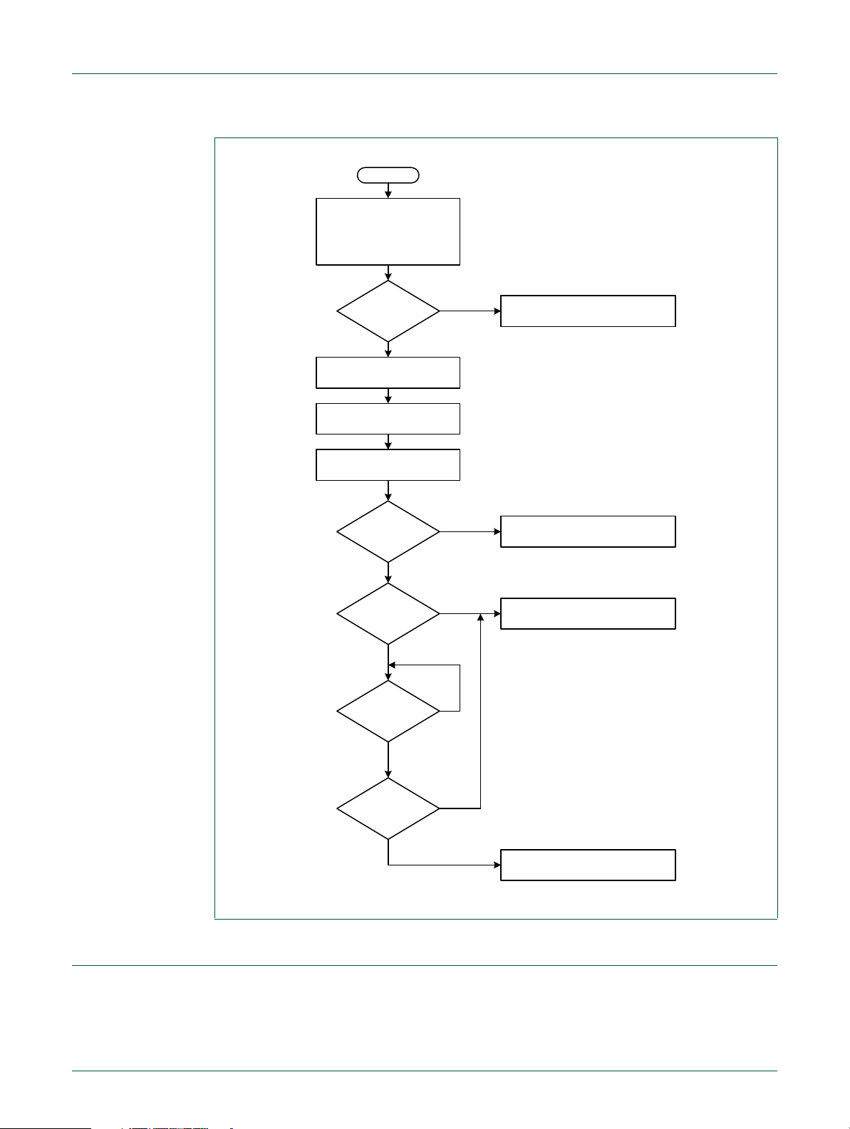
1. Introduction
2. Operation
UM10208
Chapter 3: Boot process
Rev. 02 — 31 May 2007 User manual
Upon reset, the LPC288x executes code from an internal ROM. This code allows four
possible types of startup. These are:
• Execute code from internal flash memory.
• Execute code from external memory bank 0.
• Download code from USB to memory.
• Test mode. Toggles a port pin to indicate basic device functionality.
Internal pulldowns on the P2.3 and P2.2 pins cause them to read as 0 when u nconnected.
This results in the default startup mode being execution from internal Flash memory. One
or two external pullup resistors can cause startup to use one of the other modes, as
shown in Table 3–3
Table 3. Boot flow chart
P2.3/Mode2 P2.2/Mode1 Mode selected
0 0 Execute user program from internal flash memory.
0 1 Execute user program from external memory on bank 0.
1 0 Download program from USB port to memory.
1 1 Test mode.
.
3. Boot mode descriptions
The boot process is illustrated in figure 1. The following discussion describes each boot
mode in more detail.
Mode 0: Execute user program from internal flash memory
This is the default mode if the P2.3 and P2.2 pins are left unconnected. The Flash
memory begins at address 0x1040_0000. This is the address branched to in this mode.
In order to prevent accidental execution of an unprogrammed Flash, the ROM code
checks for a specific valid user program marker value in memory prior to branching into
the Flash memory. This marker is stored as address 0x104F_F800, 2K bytes below the
top of the 1MB Flash memory. The value expected here is 0xAA55_AA55. If Mode 0 is
selected and the valid user program marker va lue is not fo un d in the Fla s h , con tr ol is
transferred to Mode 2 (USB download mode ).
UM10208_2 © NXP B.V. 2007. All rights reserved.
User manual Rev. 02 — 31 May 2007 10 of 362
Page 11

NXP Semiconductors
Mode 1: Execute user program from external memory on static memory bank 0
Static bank 0 of external memory controller is used in a default configuration to execute a
user program. The configuration of static bank 0 following reset is for a bus wid th of 16 bit s
and an active low chip select. The starting address used for the external static memory is
0x2000_0000. The full address range for bank 0 is 0x4000_000 0 through 0x401F_FFFF,
a 2 megabyte space.
Mode 2: Download program from USB port to memory (DFU mode)
The purpose of this mode is to allow programming of the internal Flash memory via USB.
Files to be download must be specially formatted in order to be handled by the ROM
download code. A conversion program and a DFU downloader are available from Philips.
Mode 3: Test mode
This mode is a simple test for device function. Port pin P2.1 is toggled to indicate basic
functionality of the device in its current environment.
UM10208
Chapter 3: LPC2800 Boot process
UM10208_2 © NXP B.V. 2007. All rights reserved.
User manual Rev. 02 — 31 May 2007 11 of 362
Page 12
NXP Semiconductors
Basic Initialization
- disable interrupts
- disable cache
- initialize CGU
Initialize exception modes
Mode = 3?
Y
N
Initialize external memory
controller
Mode = 1?
Y
N
Mode = 2?
Y
N
Initialize internal memory
systems
Reset
- Continuously toggle pin P2.1
- Branch to first Flash address.
- USB download
- Branch to first bank 0 address.
Flash ready?
N
Valid User
Program
Marker?
N
Y
Y
UM10208
Chapter 3: LPC2800 Boot process
4. Part Identification register (SYS_PARTID - 0x8000 507C)
Fig 3. Boot process
UM10208_2 © NXP B.V. 2007. All rights reserved.
User manual Rev. 02 — 31 May 2007 12 of 362
The SYS_PARTID register contains a value that identifies this device.
Page 13

NXP Semiconductors
Table 4: Part Identification register (SYS_PARTID - 0x8000 507C)
Bit Symbol Description Reset
31:0 PART_ID This value distinguishes this device type. 0x0102 100A
UM10208
Chapter 3: LPC2800 Boot process
value
UM10208_2 © NXP B.V. 2007. All rights reserved.
User manual Rev. 02 — 31 May 2007 13 of 362
Page 14

1. Introduction
2. Features
UM10208
Chapter 4: Processor cache and memory mapping
Rev. 02 — 31 May 2007 User manual
The ARM CPU in the LPC288x has been extended with a 2-way set-associative cache
controller. The cache is 8 kB in size and can store both data and instruction code.
The biggest benefit of this cache is that if code is run from non-zero-wait sta te memory, for
instance the internal FLASH controller, these memories can still behave almost as if they
are zero-wait state memory. If code is executed from the cache, the CPU will run at 1
clock per instruction most of the time.
The trade-off in introducing this cache is that each AHB access that bypasses the cache
will have an extra wait state inserted. So, it is generally advisable that both instruction
caching and data caching are turned on for most regions of on and off-chip memory.
• 8 kB in a 2-way set-associative cache
• Configured as 2×128 cache lines of eight 32-bit words each
• Sixteen pages of address mapping each allow any address range to be selected for
caching
3. Cache definitions
• A 2-way cache includes two cache lines that can be used for each memory address.
• A cache line is 8 consecutive 32 bit words. The cache contains 128 cache lines, each
with 2 ways, making 8 kB total.
• The association of memory addresses to cache lines is that cache line 0 corresponds
with address word addresses 0x0 to 0x07, cache line 1 corresponds with word
addresses 0x08 to 0x0F, etc. After 1024 words, this repeats. Thus, word address 0,
word address 1024, word address 2048, ... all map to cache line 0.
• A tag word is associated with each cache line. The tag includes the address each
cache line is currently associated with, a "dirty" flag that indicates if the line has been
written to since it was read from memory, and a "Least Recently Used" tag that
identifies which of the two cache lines should be overwritten if another address that
maps there is accessed by the CPU.
• For the purposes of cache operation, memory is divided into pages of 2 megabytes,
composed of 4 kB sub-pages (1024 words of 32 bits).
• A cache line is marked as "dirty" when the CPU writes to an address which is
currently in the cache. In this case, the data in the "real" memory no longer reflects the
actual value. The entire cache line is marked as dirty when any element within that
cache line is written.
• A cache miss is defined as a read or write by the CPU to an address in memory which
is not currently in the cache.
UM10208_2 © NXP B.V. 2007. All rights reserved.
User manual Rev. 02 — 31 May 2007 14 of 362
Page 15

NXP Semiconductors
• A cache hit is defined as a read or write by th e CPU to an address in memory which is
• A cache flush is the act of writing a dirty cache line back to memory.
4. Description
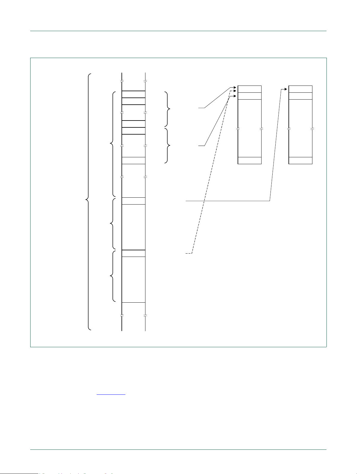
Figure 4–4 shows the structure of the cache and how memory addresses map to cache
lines. For caching purposes, memory is divided into pages of 2 megabytes of 4 kB
sub-pages (1024 words of 32 bits). The sub-pages correspond to 128 cache lines (128
entries of eight 32-bit words).
The associated cache line in memory will be stored in cache memory at a fixed position.
An example sequence could begin with an access to one of the first 8 words of a 2
megabyte page of memory. These words will be stored on the first cache line (cache line
0) of Way_0. An access to one of the second 8 words in the same page will be stored on
the second cache line (cache line 1) of Way_0. Later, if an address that maps to cache
line 0 is read from a different portion of memory, it will be stored in Way_1 (since Way_1
has not yet been used). If still another address mapping to cache line 0 is read, the Least
Recently Used tag is used to decide whether the new line will be stored in Way_0 or
Way_1. The least recently used previously cached line must be r emoved, and the new
line stored in its place. In this example, the way that is overwritten will be Way_0, since
Way_1 was used more recently. If the cache line that must be removed is marked as
“dirty”, it will be written back to memory prior to being overwritten by the new memory line.
UM10208
Chapter 4: LPC2800 Cache
currently in cache.
Note that the cache can be set to work only for instruction accesses, only for data
accesses, or for both. This is done via the DATA_ENABLE and INSTRUCTION_ENABLE
bits in the CACHE_SETTINGS register.
UM10208_2 © NXP B.V. 2007. All rights reserved.
User manual Rev. 02 — 31 May 2007 15 of 362
Page 16
NXP Semiconductors
Word 0
Word 7
Word 8
Word 15
Read into
cache line 0
Way_0
4K bytes
Word 1
2M
bytes
128 * 8
Words
Read into
cache line 1
Second read
into cache line 0
Third read into
cache line 0
Way_1
4K bytes
128 * 8
Words
128 * 8
Words
line 0
line 128
line 1
line 0
line 128
line 1
Memory
UM10208
Chapter 4: LPC2800 Cache
Fig 4. Cache operation
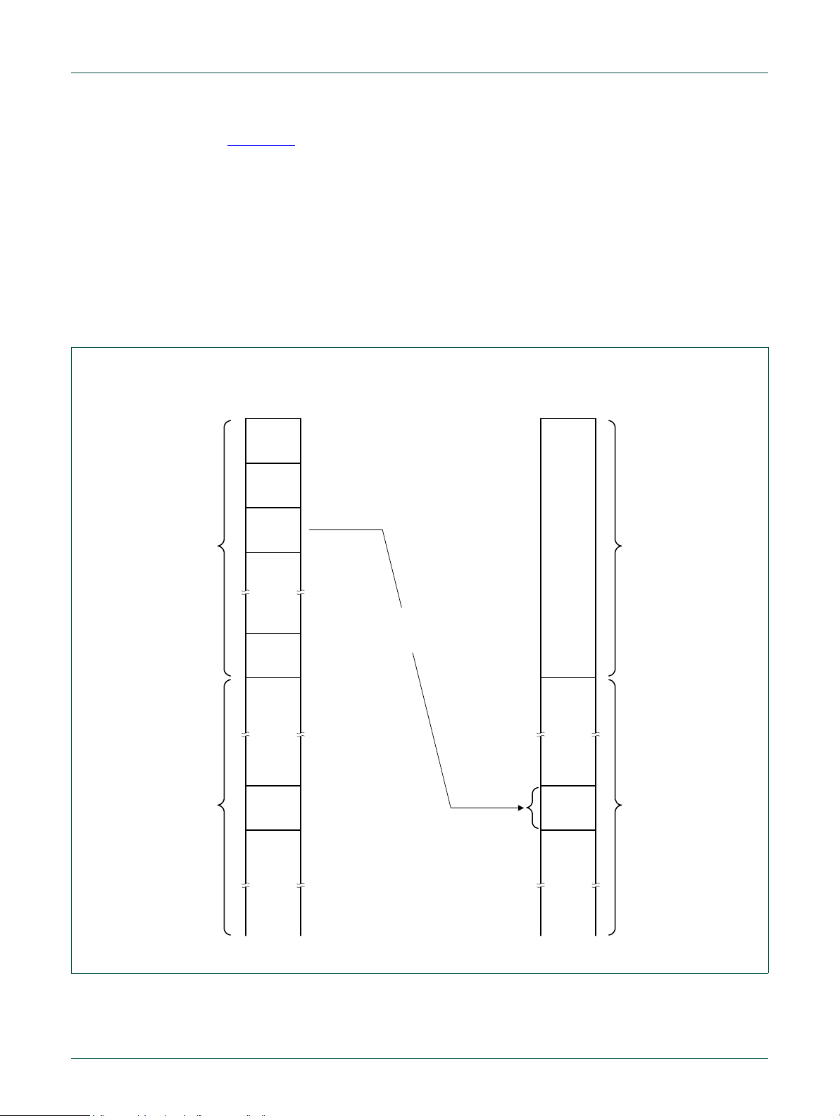
The cache has 16 configurable pages, each being 2 megabytes in size. The cache treats
these 16 pages as if they occupy the bottom 32 Megabytes of the system memory map,
which is their default mapping. The cache can re-map any of these pages such that the
physical address is above the lower 32 megabytes.
In Figure 4–5
On the left of the diagram, memory is shown with no remapping, as issued by the CPU.
, a diagram showing physical memory and a virtual page mapping is given.
On the right, a higher physical address is shown mapped into a lower address fo r caching
purposes. To accomplish this, a page is used as a virtual page. Accessing this virtual
page, the cache will re-map the AHB bus address to the higher address range during a
cache miss, cache flush or a write access to the virt ua l page.
UM10208_2 © NXP B.V. 2007. All rights reserved.
User manual Rev. 02 — 31 May 2007 16 of 362
Page 17
NXP Semiconductors
0x0000_0000
0x0020_0000
0x0040_0000
0x0200_0000
Page 0
Page 1
Page 2
Page 16
First
32 M
bytes
Above
32 M
bytes
External
SRAM
0x0000_0000
0x0200_0000
Memory
(address as seen
by the AHB bus)
First
32 M
bytes
Above
32 M
bytes
Memory
(address as issued
by the CPU)
0x0040_0000
0x2080_0000
External
SRAM
0x2080_0000
Address remapped
by value in
ADDRESS_PAGE_2
In Figure 4–5, page 2 of the lower 32 megabytes of address space has been mapped to
an address in the external static memory space by placing a value of 0x104 in the
PAGE_ADDRESS_2 register. Details of this remapping may be found in the descriptions
of the PAGE_ADDRESS registers later in this chapter.
When re-mapping points to a higher page in the memory map, that page may still also be
accessed directly by the CPU using the original absolute address of the page. In that
case, the cache takes no part in the access. This allows both cached and non-cached
access to the same address region if needed.
Each of the 16 configurable cache pages can be individually enabled and disabled, as
well as having a virtual address programmed.
UM10208
Chapter 4: LPC2800 Cache
Fig 5. Memory mapping
UM10208_2 © NXP B.V. 2007. All rights reserved.
User manual Rev. 02 — 31 May 2007 17 of 362
Page 18

NXP Semiconductors
4.1 Cache enabling and function
Following reset, the cache is disabled. The address, data, and control signals of the CPU
AHB bus is routed directly to the multilayer AHB matrix. The response from whichever
functional block is targeted by the address is routed directly to the CPU.
The cache can be enabled by setting the DATA_ENABLE and/or
INSTRUCTION_ENABLE bits in the CACHE_SETTINGS register.
4.1.1 Cache function details
For each page of the cache which is enabled, the following points apply:
• If data is read, and not in the cache (a cache miss), a lin e of eight 32-bit words is r ead
• If data is read and is found in the cache (a cache hit), data is read from cache with 0
• If data is written and the location is not in the cache (a cache miss), the data is written
• If data is written, and the location is in the cache because this location has been read
• If a dirty line is about to be discarded because of a cache miss (the cache line needs
• When a cache line is read from memory and stored in the cache (in Way_0 or
UM10208
Chapter 4: LPC2800 Cache
from the AHB bus. In the meantime, the CPU is stalled (and in low power mode if
clock gating is enabled.)
wait states.
directly to memory.
before (a cache hit), then data is written to the cache with 0 wait states, and the line is
marked as dirty.
to be reused for a different memor y region), the old line is first wr itten back to memory
(a cache line flush).
Way_1), the cache controller will mark the other half of the cache line at the same
address as Least Recently Used (LRU) in its tag memory.
5. Register description
The cache controller includes the registers shown in Table4–5. These registers are
accessible in the APB2 address space. It is recommended that the clock gating option be
enabled in the CGU for the APB interface of the CPU in order to reduce power
consumption. Each register is described in more detail in the following sections.
Note: the APB interface of the CPU configuration hardware must be set to run at the same
BASE_CLK frequency as the AHB interface of the CPU before any register is written.
Table 5. Cache and memory mapping registers
Address Register name Description Reset
0x8010 4000 CACHE_RST_STAT Monitors the reset state of the cache. 0 RO
0x8010 4004 CACHE_SETTINGS Controls the overall configuration of the cache. 0 R/W
0x8010 4008 CACHE_PAGE_CTRL Allows individual enabling or disabling of caching for the
0x8010 400C C_RD_MISSES If cache performance analysis is enabled in the
UM10208_2 © NXP B.V. 2007. All rights reserved.
User manual Rev. 02 — 31 May 2007 18 of 362
Access
value
0R/W
16 configurable pages.
0RO
CACHE_SETTINGS register, this register indicates the
number of times that a cache line is read from memory
(cache read misses).
Page 19

NXP Semiconductors
UM10208
Chapter 4: LPC2800 Cache
Table 5. Cache and memory mapping registers
Address Register name Description Reset
value
0x8010 4010 C_FLUSHES If cache performance analysis is enabled in the
CACHE_SETTINGS register, this register indicates the
number of times that a dirty cache line has been written
back to memory (cache flushes).
0x8010 4014 C_WR_MISSES If cache performance analysis is enabled in the
CACHE_SETTINGS register, this register indicates the
number of times that a write occurs to an address not in
the cache (cache write misses).
0x8010 4018 PAGE_ADDRESS_0 Re-mapping address for page 0. 0 R/W
0x8010 401C PAGE_ADDRESS_1 Re-mapping address for page 1. The reset value points
this page to the Boot ROM.
0x8010 4020 PAGE_ADDRESS_2 Re-mapping address for page 2. The reset value points
this page to the on-chip SRAM.
0x8010 4024 PAGE_ADDRESS_3 Re-mapping address for page 3. The reset value points
this page to the on-chip SRAM.
0x8010 4028 PAGE_ADDRESS_4 Re-mapping address for page 4. The reset value points
this page to on-chip Flash memory.
0x8010 402C PAGE_ADDRESS_5 Re-mapping address for page 5. The reset value points
this page to external static memory bank 0.
0x8010 4030 PAGE_ADDRESS_6 Re-mapping address for page 6. The reset value points
this page to external static memory bank 0.
0x8010 4034 PAGE_ADDRESS_7 Re-mapping address for page 7. The reset value points
this page to external SDRAM.
0x8010 4038 PAGE_ADDRESS_8 Re-mapping address for page 8. The reset value points
this page to external SDRAM.
0x8010 403C PAGE_ADDRESS_9 Re-mapping address for page 9. 0x400 R/W
0x8010 4040 PAGE_ADDRESS_10 Re-mapping address for page 10. 0x401 R/W
0x8010 4044 PAGE_ADDRESS_11 Re-mapping address for page 11. 0x102 R/W
0x8010 4048 PAGE_ADDRESS_12 Re-mapping address for page 12. 0x104 R/W
0x8010 404C PAGE_ADDRESS_13 Re-mapping address for page 13. 0x106 R/W
0x8010 4050 PAGE_ADDRESS_14 Re-mapping address for page 14. 0xE R/W
0x8010 4054 PAGE_ADDRESS_15 Re-mapping address for page 15. 0xF R/W
0x8010 4058 CPU_CLK_GATE Controls gating of the CPU clock when the CPU is
stalled.
0RO
0RO
0x1 R/W
0x2 R/W
0x2 R/W
0x82 R/W
0x100 R/W
0x100 R/W
0x180 R/W
0x180 R/W
0R/W
Access
5.1 Cache Reset Status register (CACHE_RST_STAT, 0x8010 4000)
The read-only CACHE_RST_STAT register monitors the re set status of the cache
controller. If the CACHE_RST bit in the CACHE_SETTINGS register is set and then
cleared by software, this bit indicates the status of the ongoing reset. The reset of the
cache tag memory will take 128 CPU clock-cycles to complete. Table 4–6
definitions for the CACHE_RST_STAT register.
UM10208_2 © NXP B.V. 2007. All rights reserved.
User manual Rev. 02 — 31 May 2007 19 of 362
shows the bit
Page 20

NXP Semiconductors
Table 6. Cache Reset Status register (CACHE_RST_STAT, 0x8010 4000)
Bit Symbol Description Reset
0 CACHE_STATUS 0: Cache reset is complete.
31:1 - Reserved. The value read from a reserved bit is not defined. -
5.2 Cache Settings register (CACHE_SETTINGS, 0x8010 4004)
The CACHE_SETTINGS register controls the general setup of the cache, allows r esetting
of the entire cache, and controls the cache performance analysis feature. Table 4–7
shows the bit definitions for the CACHE_SETTINGS register.
Table 7. Cache Settings register (CACHE_SETTINGS, 0x8010 4 004)
Bit Symbol Description Reset
0 CACHE_RST Cache controller reset control. This bit resets the cache
1 DATA_ENABLE Enables use of the cache for storing data.
2 INSTRUCTION_ENABLE Enables use of the cache for storing instructions.
UM10208
Chapter 4: LPC2800 Cache
value
0
1: Cache reset is ongoing.
When the cache is reset, sof tware should poll
CACHE_STATUS until it is 0.
value
0
hardware internally, clearing all tags so that the entire
cache is considered empty. This t akes 128 CPU clock
cycles to complete. The reset progress can be followed
by reading register CACHE_RST_STAT.
0 : De-assert reset to the Flash controller .
1 : Assert reset to the Flash controller.
Note: the cache MUST be reset before it is enabled. It is
recommended to include this procedure at system
startup.
0
0 : All storage of data in the cache is disabled. This
applies to all 16 pages.
1 : Storage of data in the cache is enabled. This applies
to all pages enabled via the CACHE_PAGE_CTRL
register.
0
0 : All storage of instructions in the cache is disabled.
This applies to all 16 pages.
1 : Storage of instructions in the cache is enabled. This
applies to all pages enabled via the
CACHE_PAGE_CTRL register.
UM10208_2 © NXP B.V. 2007. All rights reserved.
User manual Rev. 02 — 31 May 2007 20 of 362
Page 21

NXP Semiconductors
Table 7. Cache Settings register (CACHE_SETTINGS, 0x8010 4 004)
Bit Symbol Description Reset
3 PERF_ANAL_RST Allows a software reset of the cache performance
UM10208
Chapter 4: LPC2800 Cache
value
0
analysis counters in the registers C_RD_MISSES,
C_FLUSHES, and C_WR_MISSES.
0 : Allow performance analysis counters to run, if
enabled.
1 : Reset the cache performance analysis counters.
This has an effect only if performance analysis is
enabled.
4 PERF_ANAL_ENA Controls the cache performance analysis counters in
the registers C_RD_MISSES, C_FLUSHES, and
C_WR_MISSES. Performance analysis should be
disabled when not needed in order to save power.
0 : Performance analysis is disabled.
1 : Performance analysis is enabled.
31:5 - Reserved. Do not write 1s to reserved bits. The values
read from reserved bits is not defined.
5.3 Cache Page Enable Control register (CACHE_PAGE_CTRL, 0x8010 4008)
The CACHE_P AGE_CTRL register a llows individual enabling of caching of each of the 16
pages. Table 4–8
Table 8. Cache Page Enable Control register (CACHE_PAGE_CTRL, 0x8010 4008)
Bit Symbol Description Reset
0 PAGE_0_ENA This bit enables caching for page 0.
1 PAGE_1_ENA This bit enables caching for page 1, as described for bit 0. 0
2 PAGE_2_ENA This bit enables caching for page 2, as described for bit 0. 0
3 PAGE_3_ENA This bit enables caching for page 3, as described for bit 0. 0
4 PAGE_4_ENA This bit enables caching for page 4, as described for bit 0. 0
5 PAGE_5_ENA This bit enables caching for page 5, as described for bit 0. 0
6 PAGE_6_ENA This bit enables caching for page 6, as described for bit 0. 0
7 PAGE_7_ENA This bit enables caching for page 7, as described for bit 0. 0
8 PAGE_8_ENA This bit enables caching for page 8, as described for bit 0. 0
9 PAGE_9_ENA This bit enables caching for page 9, as described for bit 0. 0
10 PAGE_10_ENA Thi s bit enables caching for page 10, as described for bit 0. 0
11 PAGE_11_ENA This bit enables caching for page 11, as described for bit 0. 0
12 PAGE_12_ENA Thi s bit enables caching for page 12, as described for bit 0. 0
13 PAGE_13_ENA Thi s bit enables caching for page 13, as described for bit 0. 0
shows the bit definitions for the CACHE_PAGE_CTRL register.
0: Caching for this page is disabled.
1: Caching for this page is enabled.
0
-
value
0
UM10208_2 © NXP B.V. 2007. All rights reserved.
User manual Rev. 02 — 31 May 2007 21 of 362
Page 22

NXP Semiconductors
Table 8. Cache Page Enable Control register (CACHE_PAGE_CTRL, 0x8010 4008)
Bit Symbol Description Reset
14 PAGE_14_ENA Thi s bit enables caching for page 14, as described for bit 0. 0
15 PAGE_15_ENA Thi s bit enables caching for page 15, as described for bit 0. 0
31:16 - Reserved. Do not write 1s to reserved bits. The values read
Note: If data caching has been enabled for a writable page, and software then disables
caching, there may be “dirty data” in the cache that still needs to be written to memory.
5.4 Cache Read Misses counter (C_RD_MISSES, 0x8010 400C)
The C_RD_MISSES register allows reading the number of times that a cache line fill has
occurred (a cache read miss) since the last time that the performance analysis registers
have been reset. The counter only operates if pe rformance analysis has been e nabled via
the PERF_ANAL_ENA bit in the CACHE_SETTINGS register. In order to save power,
performance analysis should be turned off if it is not actually being used.
UM10208
Chapter 4: LPC2800 Cache
value
-
from reserved bits is not defined.
5.5 Cache Flushes counter (C_FLUSHES, 0x8010 4010)
The C_FLUSHES register allows reading the number of times that a cache line has been
written back to memory (a cache flush) since the last time that the performance analysis
registers have been reset. A cache line is written back to memory only if it has been
marked as dirty (due to its contents being changed) and the cache line is subsequently
required for normal continuing cache operation. The co unter only operates if perfor mance
analysis has been enabled via the PERF_ANAL_ENA bit in the CACHE_SETTINGS
register. In order to save power, performance analysis should be turned off if it is not
actually being used.
5.6 Cache Write Misses counter (C_WR_MISSES, 0x8010 4014)
The C_WR_MISSES register allows reading the number of times that a write has
occurred to a memory address that is not in the cache (a cache write miss). The counter
only operates if performance analysis has been enabled via the PERF_ANAL_ENA bit in
the CACHE_SETTINGS register. In order to save power, performance analysis should be
turned off if it is not actually being used.
5.7 Page Address Pointer Registers (PAGE_ADDRESS0:15, 0x8010 4018:4054)
The 16 P AGE_ADDRESS registers allow remapping of addresses in the range supported
by the cache (the bottom 32 megabytes of memory space) so that they apply to other
address ranges. When the CPU performs an access to an address in the cache range,
any value in the related PAGE_ADDRESS register will replace the top 11 bits of the 32-bit
address. By leaving the bottom 21 bits unaltered, each increment of the value in an
P AGE_ADDRESS register corresponds to a shift of 2 megabytes. In this manner , software
can control which memory address ranges are cached.
For example, if the CPU accesses the address 0x0121_4A90, and the
PAGE_ADDRESS_9 register contains the value 0x82, caching activity and the CPU
access will apply to address 0x1041_4A90:
UM10208_2 © NXP B.V. 2007. All rights reserved.
User manual Rev. 02 — 31 May 2007 22 of 362
Page 23

NXP Semiconductors
Original address: 0121_4A90 = 0000 0001 0010 0001 _ 0100 1010 1001 0000
Top 11 address bits removed: 0000 0000 000
Address bits from PAGE_ADDRESS9 (082) = 0001 0000 010
Top 11 address bits replaced:1041_4A90 = 0001 0000 0100 0001 _ 0100 1010 1001 0000
This particular setting maps page 9 of the cacheable address space to the on-chip Flash
memory starting at address 0x1040_0000.
UM10208
Chapter 4: LPC2800 Cache
0 0001 _ 0100 1010 1001 0000
Table 4–9
and Table 4–10
Table 9. Address ranges used by PAGE_ADDRESS registers
Register 2 megabyte
PAGE_ADDRESS_0 0 0x0000 0000 0x001F FFFF
PAGE_ADDRESS_1 1 0x0020 0000 0x003F FFFF
PAGE_ADDRESS_2 2 0x0040 0000 0x005F FFFF
PAGE_ADDRESS_3 3 0x0060 0000 0x007F FFFF
PAGE_ADDRESS_4 4 0x0080 0000 0x009F FFFF
PAGE_ADDRESS_5 5 0x00A0 0000 0x00BF FFFF
PAGE_ADDRESS_6 6 0x00C0 0000 0x00DF FFFF
PAGE_ADDRESS_7 7 0x00E0 0000 0x00FF FFFF
PAGE_ADDRESS_8 8 0x0100 0000 0x011F FFFF
PAGE_ADDRESS_9 9 0x0120 0000 0x013F FFFF
PAGE_ADDRESS_10 10 0x0140 0000 0x015F FFFF
PAGE_ADDRESS_11 11 0x0160 0000 0x017F FFFF
PAGE_ADDRESS_12 12 0x0180 0000 0x019F FFFF
PAGE_ADDRESS_13 13 0x01A0 0000 0x01BF FFFF
PAGE_ADDRESS_14 14 0x01C0 0000 0x01DF FFFF
PAGE_ADDRESS_15 15 0x01E0 0000 0x01FF FFFF
shows the address ranges covered by each of the PAGE_ADDRESS registers,
shows the use of bits in each register.
multiple
Bottom of related
address range
Top of related
address range
Table 10. Page Address Pointer Registers (PAGE_ADDRESS0:15, 0x8010 4018:4054)
Bit Symbol Description Reset
value
10:0 UPPR_ADDR This value will replace the top 11 bits of the 32-bit
address coming from the CPU. When the CPU performs
an access to the related page, the address which is
placed on the AHB bus will depend on the value of this
register.
31:11 - Reserved. Do not write 1s to reserved bits. The values
read from reserved bits is not defined.
see
Table 4–5
-
5.8 CPU Clock Gate control (CPU_CLK_GATE, 0x8010 4058)
The CPU_CLK_GATE register allows saving power by gating the CPU clock when the
CPU is stalled waiting for bus access. Table 4–11
CPU_CLK_GATE register.
UM10208_2 © NXP B.V. 2007. All rights reserved.
User manual Rev. 02 — 31 May 2007 23 of 362
shows the bit definitions for the
Page 24

NXP Semiconductors
Table 11. CPU Clock Gate control (CPU_CLK_GATE, 0x8010 4058)
Bit Symbol Description Reset
0 CPU_CLK_GATE This bit controls clock gating to the CPU. When clock gating is
enabled, power is saved by not clocking the CPU when it is
stalled waiting for bus access.
0: The CPU clock is running continuously.
1: The CPU clock is gated off while the CPU is stalled.
31:1 - Reserved. Do not write 1s to reserved bits. The values read
from reserved bits is not defined.
6. Cache programming procedures
6.1 Cache initialization
1. Clear the cache:
Set and reset the CACHE_RST bit in the CACHE_SETTINGS register (one clock
cycle is sufficient).
The status flag CACHE_RST_STAT in the CACHE_STATUS indicates whether a
cache reset is ongoing. Software should poll this bit before the cache is enabled.
2. Program the virtual address for each page, if needed:
Software can enable those parts of the memory map that are to be cacheable, by
setting the appropriate bits in the CACHE_PAGE_CTRL register.
Each bit represents one page (2 megabytes) of memory space:
– bit 0 enables 0x0000_0000 to 0x0020_0000 as cached (page 0),
– bit 1 enables 0x0020_0000 to 0x0040_0000 as cached (page 1),
– bit 2 enables 0x0040_0000 to 0x0060_0000 as cached (page 2),
– etc.
3. Program the virtual address for each page, if needed:
The 11 bits programmed for each page represents the top 11 bits of a 32-bit address
that will be put on the AHB bus. This allows any part of the entire 32-bit address range
to be remapped into the bottom 32 megabytes of space, in pages of 2 megabytes.
The PAGE_ADDRESS registers DO NOT reset to a value such that remapping is not
in force, so they should always be initialized even if remapping is not needed in the
application.
Example:
Say address location 0x10400000 (in on-chip Flash) must be mapped for page 3.
That can be done this way:
*PAGE_ADDRESS_3 = (0x10400000 >> 21); // = 0x082;
If the CPU reads address 0x00600004 (an address inside page 3) , then address
0x10400004 is provided to the AHB bus.
Note: care must be taken if remapping a page from which the code is currently
running, or a page that is being used for data, stack or heap storage.
4. Enable the cache for data and /or instructions:
UM10208
Chapter 4: LPC2800 Cache
value
0
-
UM10208_2 © NXP B.V. 2007. All rights reserved.
User manual Rev. 02 — 31 May 2007 24 of 362
Page 25

NXP Semiconductors
6.2 Cache flushing
Cache flushing may be required if caching of data is enabled, or when the virtual address
of a page must be changed while this page has caching enabled. Cache flushing is only
necessary if data-caching is enabled.
UM10208
Chapter 4: LPC2800 Cache
Enable the cache by setting the DATA_ENABLE and/or INSTRUCTION_ENABLE bits
in the CACHE_SETTINGS register.
For enabling cache functions, these two bits apply to all cache pages that ar e enabled
via the CACHE_P AGE_CTRL register. For disabling cache functions, these bits apply
to all 16 cache pages, regardless of the setting of the CACHE_PAGE_CTRL register.
The entire cache can be programmed to:
– cache only instructions
– cache only data
– cache both instructions and data
If neither of the two enable bits is set, the cache is disabled.
If data is written to cached memory , the new dat a will initially end up only inside the cache,
and the related cache line marked as dirty. This data is not yet stored in the true physical
location in memory. Since the cache applies only to the ARM7, not to other AHB masters,
if another master (such as the GPDMA) is programmed to copy this data, it will copy the
old data. If the programmer want s to guarantee that the d at a inside the cache is written to
memory, the programmer has to flush the cache.
The cache controller does not include a direct method to cause an immediate cache flush .
If software needs to flush the entire cache, a simple way to accomplish this is to fill the
cache with read-only data (for instance ROM data). This results in every cache line being
checked to see if it is dirty, and written back to memory if needed. Only 1 out of the 8
words from memory corresponding to each cache line must be read in order to flush one
cache line. A total of 256 cache lines must be read in order to fully flush the cache. Below
is a C language example to replace the cache contents, thereby flushing its the cache.
void flush_cache (int * cache_start) {
volatile int * flush_pointer = (volatile int *) cache_start;
volatile int cache_dummy;
int i;
for (i=0;i<2048;i+=8) cache_dummy = flush_pointer[i];
}
Example: Calling the flush_cache procedure with a value of 0x1200 will read 8 kB of
read-only code starting from 0x1200 into the cache, ef fectively flushing all dirty data from
the cache.
A subset of this procedure could be used to flush a portion of the cache (as little as one
cache line) if the line and its original address is known. Any two data locations other than
the location of the currently cached data that maps to the same cache line can be read.
This will cause any of the originally cached data to be flushed if it is marked as dirty.
Cache flushing may be necessary in the following cases:
UM10208_2 © NXP B.V. 2007. All rights reserved.
User manual Rev. 02 — 31 May 2007 25 of 362
Page 26

NXP Semiconductors
1. When data caching is enabled for a page , and another bus master such as the GPMA
2. When data caching is enabled for a page, and caching for this page is about to be
3. When data caching in the CACHE_SETTINGS register is about to be disabled. This is
4. When the virtual address of a cached page is about to be changed. This applies for
6.3 Avoiding cache flushing
It may be possible to avoid cache flushing in some cases. If the performance dif ference is
not critical, data caching can simply not be enabled. Performance reductions in the 20 to
30% range are possible if data caching is disabled, depending on the application.
UM10208
Chapter 4: LPC2800 Cache
uses this data as well.
disabled. When the caching for a page is disabled, every word is read directly from
memory , bypassin g the cache. If any dat a has been written to that p age, the CPU may
read the wrong data.
a more general version of case 2.
both instruction and data caching. The cache controller is not aware of any changes
made to the address mapping. If the address mapping is changed, software must
ensure that any altered cache contents are flushed. Also, if code was executed from
the page that is about to be remapped, it must be flushed to prevent later execution of
the wrong instructions.
Another way to avoid data caching in certain cases is to have 2 pages that point to the
same memory address range. One page would be set as cacheable, the other as not
cacheable. Data written to the non-cached page is written dire ctly to memory , so other bus
masters can make use of this data without any need to flush the ca che. Ca re mus t be
taken not to write data to one p age, and read the same dat a from the othe r page . This can
be done by separating portions of the page that may be changing from portions that will
not be changing. Changeable portions would be both read and written in the non-cached
address range, while static data would be read from the cached address range.
6.4 CPU and cache clocking
The CPU clocking is somewhat different than the rest of the AHB system. Where the rest
of the AHB system is clocked by the CGU (the AHB-BASE_CLOCK, possibly modified by
a fractional divider), the CPU and cache system use the AHB clock as a reference to
generate internal clocks from the AHB_BASE_CLOCK. Inside the cache system is a
clock-gate that uses the reference clock to enable or disable the base clock going to the
CPU and cache system.
Figure 4–6
show some internal signals to illustrate the timing. First, “CPU clock” is the clock as seen
by the CPU. Second, “CPU clock enable” is the signal that determines when the CPU
receives a clock when clock gating is enabled. The CPU clock enable signal goes low one
AHB clock prior to the time when the CPU clock is prevented.
Following is a description of each case shown:
shows timing of some cases of different clock selection settings. These figu res
1. CPU clock gating off, fractional divider not used.
In this case, there is no CPU clock-gating and a fractional di vider for the AHB clock is
not selected. This results in a free-running clock for the AHB, cache and CPU, all
running at the same frequency. This is the reset condition of the system.
UM10208_2 © NXP B.V. 2007. All rights reserved.
User manual Rev. 02 — 31 May 2007 26 of 362
Page 27
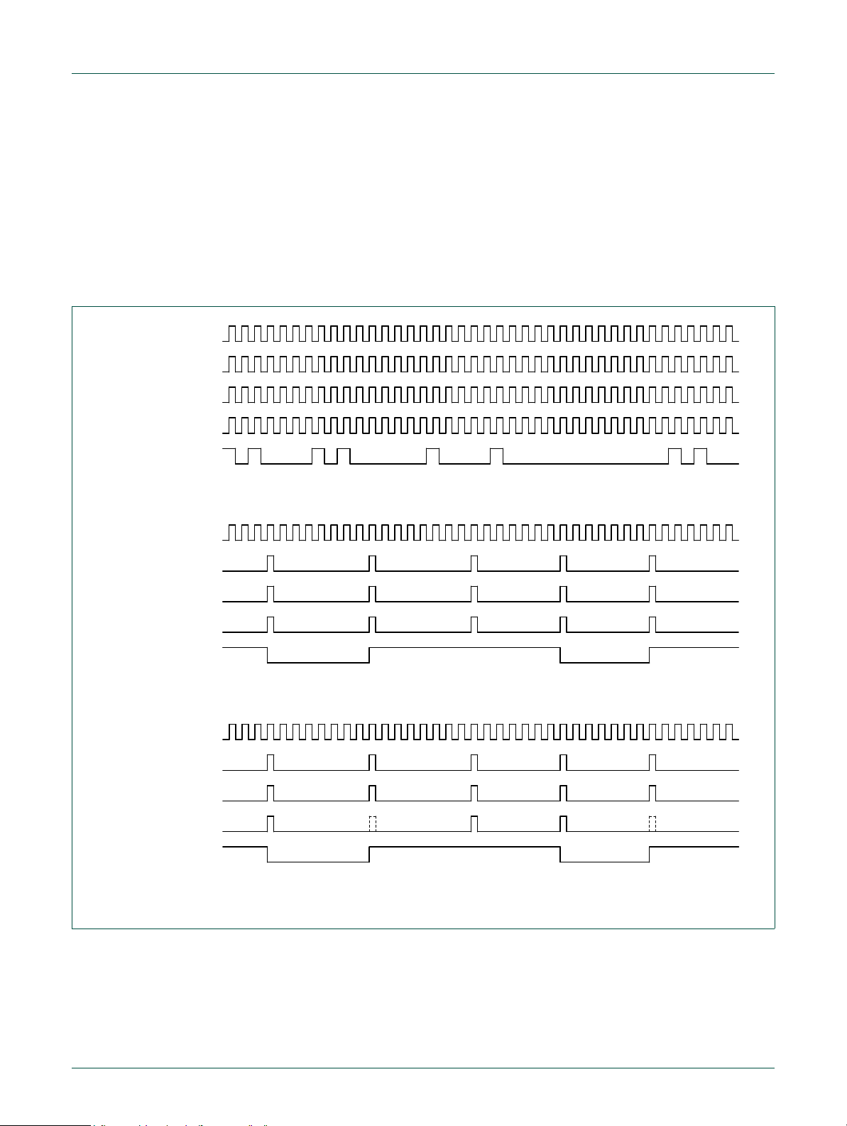
NXP Semiconductors
CPU clock
AHB0 clock
Internal cache clock
Internal CPU clock
CPU clock enable
Case 1: CPU clock gating off, fractional divider not used.
CPU clock
AHB0 Clock
Internal cache clock
Internal CPU clock
CPU clock enable
Case 2: CPU clock gating off, fractional divider set to 1/7.
CPU clock
AHB0 Clock
Internal cache clock
Internal CPU clock
CPU clock enable
Case 3: CPU clock gating enabled, fractional divider set to 1/7.
2. CPU clock gating off, fractional divider set to 1/7.
3. CPU clock gating enabled, fractional divider set to 1/7.
UM10208
Chapter 4: LPC2800 Cache
In this case, the AHB fractional divider has been set to generate a bus clock once
every 7 base clock cycles.
In this case, CPU clock gating has been enabled. The CPU clock enable signal is
generated by the cache when the CPU must wait because either the cache is read ing
or writing data on the AHB bus, or the cache is jumping in between cache lines,
adding a single wait state.
Fig 6. Cache and CPU clock timing
UM10208_2 © NXP B.V. 2007. All rights reserved.
User manual Rev. 02 — 31 May 2007 27 of 362
Page 28

1. Introduction
2. Features
3. Description
UM10208
Chapter 5: Flash interface and programming
Rev. 02 — 31 May 2007 User manual
The LPC2888 includes one megabyte of flash memory. This memory is located on the
AHB and is accessible by all AHB masters. In contrast, the LPC2880 does not include any
on-chip flash memory.
• Flash memory is an AHB slave for data transfer.
• APB slave interface for programmatic flash programming and erasure.
• Interrupt capability when flash erasure or programming is completed.
The flash memory controller has an AHB slave port for transfer of instructions and dat a to
the CPU in response to normal read requests. There is also a APB port for configuring the
Flash controller and for accomplishing programming functions.
3.1 Flash organization
The Flash memory is organized into 64 kB large sectors and 8 kB small sectors. For
1 MB of total Flash, there are 15 large sectors and 8 small sectors. The organization of
these sectors and corresponding add ress ra ng e s is shown in Figure 5–7
The flash memory produces 128 bits of data for each read operation. These four words
of data are referred to as a flash word. During progra mming, four flash words are
programmed at a time.
.
3.2 Flash buffering
Because the Flash memory is 128 bits wide, while the AHB is a 32 bit interface, a buffer
between the Flash memory and the AHB can reduce power by limiting the number of
Flash reads required, as well as speed up response to reads of consecutive Flash
locations.
A Flash read is a slow process compared to the AHB cycle time. With buffering, the
average read time is reduced, which can improve system performance. A single level
buffer receives data from a Flash read and retains it until another flash read is required.
When an AHB read requires data from the same Flash Wor d as the previous read, a Flash
read is not performed, and read data is given without wait states. During sequential
program execution, a Flash read will only be required for every fourth ARM instruction, or
every eighth Thumb instruction.
When an AHB read requires data from a different Flash Word than the previous read, a
new Flash read is performed and wait states occur until the new read data is available.
The flash buffer is automatically invalidated after:
UM10208_2 © NXP B.V. 2007. All rights reserved.
User manual Rev. 02 — 31 May 2007 28 of 362
Page 29

NXP Semiconductors
8KB small sector # 7
64KB large sector # 14
64KB large sector # 13
64KB large sector # 3
64KB large sector # 4
64KB large sector # 5
64KB large sector # 6
64KB large sector # 7
64KB large sector # 8
64KB large sector # 9
64KB large sector # 10
64KB large sector # 11
64KB large sector # 12
64KB large sector # 2
64KB large sector # 1
64KB large sector # 0
8KB small sector # 5
8KB small sector # 4
8KB small sector # 3
8KB small sector # 2
8KB small sector # 1
8KB small sector # 0
8KB small sector # 6
0x1040_0000 to 0x1040_FFFF
0x1041_0000 to 0x1041_FFFF
0x1042_0000 to 0x1042_FFFF
0x1043_0000 to 0x1043_FFFF
0x1048_0000 to 0x1048_FFFF
0x1047_0000 to 0x1047_FFFF
0x1046_0000 to 0x1046_FFFF
0x1045_0000 to 0x1045_FFFF
0x1044_0000 to 0x1044_FFFF
0x104F_0000 to 0x104F_1FFF
0x104E_0000 to 0x104E_FFFF
0x104D_0000 to 0x104D_FFFF
0x104C_0000 to 0x104C_FFFF
0x104B_0000 to 0x104B_FFFF
0x1049_0000 to 0x1049_FFFF
0x104A_0000 to 0x104A_FFFF
0x104F_2000 to 0x104F_3FFF
0x104F_4000 to 0x104F_5FFF
0x104F_C000 to 0x104F_DFFF
0x104F_A000 to 0x104F_BFFF
0x104F_8000 to 0x104F_9FFF
0x104F_6000 to 0x104F_7FFF
0x104F_E000 to 0x104F_FFFF
• Chip initialization
• An access to a flash configuration register
• Data latch reading (described in Section 5–4 “In-Application flash programming” on
UM10208
Chapter 5: LPC2800 Flash
page 30)
UM10208_2 © NXP B.V. 2007. All rights reserved.
User manual Rev. 02 — 31 May 2007 29 of 362
Fig 7. Flash sector organization
Page 30

NXP Semiconductors
3.3 Wait state programming
The Flash controller takes data from the memory after a predefined number of clock
cycles. These clock cycles are called wait states and can be programmed in the
WAIT_STATES field of the F_WAIT register. The optimal number of wait states de pends
on the clock frequency of the AHB clock. As a result, the number of wait states should
typically be changed if the CPU clock rate is changed. To prevent incorrect reads, wait
states should be changed to a larger value just before increasing the CPU clock rate, or
changed to a smaller value just after decreasing the CPU clock rate.
4. In-Application flash programming
4.1 Introduction
Programming the embedded flash memory requires a specific sequence of events,
controlled primarily by software.
UM10208
Chapter 5: LPC2800 Flash
The flash memory is organized in sectors, as shown in Figure 5–7
before data can be written into them. The flash memory also has built in protection against
accidental programming.
As software write words to addresses in the Flash memory address range (0x104x xxxx),
the hardware transfers a Flash word (4 words, 16 bytes) into an internal page buffer, af ter
each write to an address 0x104x xxxC. A Flash page is the unit in which the Flash is
programmed: 512 bytes.
Figure 5–8
shaded part of the flow chart represents functions that are done au to m atic ally by the
hardware of the flash controller.
shows a flow chart for programming the flash memory on the LPC2888. The
, that must be erased
UM10208_2 © NXP B.V. 2007. All rights reserved.
User manual Rev. 02 — 31 May 2007 30 of 362
Page 31

NXP Semiconductors
Un-Protect sector(s)
Erase sector(s)
Preset data latches
Write Word
(auto) Load Flash
Load Flash Word
Program Flash Page
Protect sector(s)
Flash Word
complete?
Page
complete?
Sector(s)
complete?
Last
Flash Word
complete?
N
Y
Y
N
Y
N
Y
N
UM10208
Chapter 5: LPC2800 Flash
Fig 8. Flash AHB programming flow chart
Flash programming includes the following steps:
UM10208_2 © NXP B.V. 2007. All rights reserved.
User manual Rev. 02 — 31 May 2007 31 of 362
1. Un-protecting the sectors to be operated upon
2. Erasing sectors that have been previously programmed
3. Presetting data latches for each flash word to be programmed
4. Writing
5. Loading
6. Programming
Page 32

NXP Semiconductors
7. Restoring protection to sectors that have been operated upon
These steps are described in more detail in the following sections.
4.2 Sector protection and un-protection
A sector is unprotected by writing an even value to its base address (the starting address
of the sector), followed by writing the unprotect trigger value to the F_CTRL register. The
trigger value for (un)protecting has the following bits set: FC_LOAD_REQ,
FC_PROTECT, FC_WEN, FC_FUNC, and FC_CS. The ot he r bits are zero .
A sector is protected by writing an odd value to its base address, followed by the same
trigger value that was used to unprotect the sector.
4.3 Erasing sectors
First, a sector to be erased must be unprotected as described above. Before the erasing,
the erase time must be selected in the timer register FPT_TIME field of the
F_PROG_TIME register, and the timer must be enabled via the FPT_ENABLE field of the
in the same register. During erasing, the timer register counts down to zero. Therefore, the
timer register must be rewritten prior to every erase cycle.
UM10208
Chapter 5: LPC2800 Flash
The programmed erase time must satisfy the requirement:
(512 × FPT_TIME + 2) × (AHB clock time) ≥ 400ms
Which is to say, write FPT_TIME with the integer greater than or equal to:
((400,000,000 / AHB t
A single sector is erased by writing any value to an address within that sector, followed by
writing the erase trigger value to the F_CTRL register. The trigger value for erasing has
the following bits set: FC_PROG_REQ, FC_PROTECT, and FC_CS. The other bits are
zero.
For erasing and other programmi ng ope rat io n s, the Fla sh mod u l e ne ed s a 66 kHz cl ock .
This clock is derived from the AHB clock, dividing it by a factor programmed in the
CLK_DIV field of the F_CLK_TIME register. A value of zero in this field inactivates the
FLASH PROGRAMMING clock.
Erasing multiple sectors can be done with only one longer erase cycle. First all sectors
except the last are selected for erasure. Then the last sector is erased using the single
sector erase procedure. A sector is selected for er as ur e by wr iting any value to an
address within that sector, followed by writing the select for erase trigger value to the
F_CTRL register. This trigger value has the following bits set: FC_LOAD_REQ,
FC_PROTECT, FC_WEN, and FC_CS. The other bits are zero.
The Flash controller can optionally generate an interrup t request when erasing is finished,
otherwise the FS_DONE flag in the F_STAT register can be polled by software to
determine when erasure is complete.
(in ns)) - 2) / 512
cyc
UM10208_2 © NXP B.V. 2007. All rights reserved.
User manual Rev. 02 — 31 May 2007 32 of 362
Page 33

NXP Semiconductors
4.4 Presetting data latches
The Flash memory has data latches to store the data that is to be programmed into the
Flash array. When only a part of a Flash page (512 bytes) has to be programmed, the data
latches for the rest of the page must be preset to logical ones. This can be done with a
single control by setting and clearing the FC_SET_DATA bit in the F_CTRL register.
It is possible to read back the data latches by setting bit FD_RD_LATCH in the F_CTRL
register.
4.5 Writing and loading
Writing a Word to the Flash controller is done via the AHB. Every write takes 2 clock
cycles (1 wait state), and results in a partial update of the data input of the Flash module.
Writing is done one word at a time. Byte or halfword writing is not possible. However,
because writing logical ones leaves the Flash contents unchanged, it is possible to do
byte writing by encapsulating this byte in a Word of logical ones. This encapsulation must
be done by the AHB master that initiates the transfer.
Every fourth write, a Flash Word (four data words) is loaded automatically into the data
latches of the Flash module. Loading is done per Flash Word.
UM10208
Chapter 5: LPC2800 Flash
For example, when addresses 0x00 through 0x0C are to be loaded, loading is done
automatically after writing to address 0x0C (note that these four addresses form a single
complete Flash Word). This requires that values are already written to addresses 0x00 to
0x08.
Loading can also be done manually by writing a 1 to the FC_LOADREQ bit in the F_CTRL
register.
4.6 Programming
First, a sector to be erased must be unprotected as previous ly described. Progr amming is
the data transfer from the data latches of the Flash module into the Flash array. Before
programming, the programming time must be written to the FPT_TIME field of the
F_PROG_TIME register, and the timer must be enabled via the FPT_ENABLE bit in the
F_PROG_TIME register. During programming, the timer register counts down to zero.
Therefore, the timer register must be rewritten before every programming cycle.
The programmed programming time must satisfy the requirement:
(512 × FPT_TIME + 2) × (AHB clock time) ≥ 1ms
Which is to say, write FPT_TIME with the integer greater than or equal to:
((1,000,000 / AHB tcyc (in ns)) - 2) / 512
Programming is started by writing a trigger value to the F_CTRL register. The trigger value
for programming has the following bits set: FC_PROG_REQ, FC_PROTECT, FC_FUNC,
and FC_CS. The other bits are zero.
The page address that is offered to the Flash modu le during programming is the page
address of the most recent write to an address within the Flash memory range.
UM10208_2 © NXP B.V. 2007. All rights reserved.
User manual Rev. 02 — 31 May 2007 33 of 362
Page 34

NXP Semiconductors
For programming and erase op er a tion s, the Flash module needs a 66 kHz clock. This
clock is derived from the AHB clock, dividing it by a factor programmed in the CLK_DIV
field of the F_CLK_TIME register. A value of zero in this field inactivates the FLASH
PROGRAMMING clock.
The flash controller can optionally generate an interrupt requ est when programming is
finished.
4.7 Program/erase timer
A built-in timer is used to control the program time or erase time. The timer is started by
writing the program or erase time to the FPT_TIME field of the F_PROG_TIME register,
and by enabling it via the FPT_ENABLE bit in the same register. During programming or
erasing, the timer register counts down to zero, and its current value is returned when
reading the F_PROG_TIME register. This timer reading can be used to observe the
progress of programming/erasing.
While the timer is counting down, the flash memory controller is only partly accessible:
• Reads of the flash memory are stalled, using AHB wait states.
• Writes to the flash controller registers are stalled.
• Reads of flash controller registers are completed normally without stalling.
UM10208
Chapter 5: LPC2800 Flash
This can have significant impact on system behavior. It should be insured that the Flash
memory is not busy (the FPT_TIME field in the F_PROG_TIME register = 0 and the
FS_RDY bit in the F_STAT register =1) prior to attempting to read Flash data or write to a
Flash controller register.
5. Register description
The Flash memory controller has registers to set the wait states for normal operation and
registers to control program/erase operations. Flash controller registers are listed in
Table 5–12
Table 12. Flash memory controlle r registers
Offset Register name Description Access Reset
0x8010 2000 F_CTRL Flash control register R/W 0x5
0x8010 2004 F_STAT Flash status register RO 0x45
0x8010 2008 F_PROG_TIME Flash program time register R/W 0
0x8010 2010 F_WAIT Flash read wait state register R/W 0xC004
0x8010 201C F_CLK_TIME Flash clock divider for 66 kHz
0x8010 2FD8 F_INTEN_CLR Clear interrupt enable bits WO 0x8010 2FDC F_INTEN_SET Set interrupt enable bits WO 0x8010 2FE0 F_INT_STAT Interrupt status bits RO 0
0x8010 2FE4 F_INTEN Interrupt enable bits RO 0
0x8010 2FE8 F_INT_CLR Clear interrupt status bits WO -
.
value
R/W 0
generation
UM10208_2 © NXP B.V. 2007. All rights reserved.
User manual Rev. 02 — 31 May 2007 34 of 362
Page 35

NXP Semiconductors
UM10208
Chapter 5: LPC2800 Flash
Table 12. Flash memory controlle r registers
Offset Register name Description Access Reset
value
0x8010 2FEC F_INT_SET Set interrupt status bits WO 0x8000 5030 FLASH_PD Allows turning off the Flash memory
for power savings.
0x8000 5034 FLASH_INIT Monitors Flash readiness, such as
recovery from Power Down mode.
R/W 1
R/W -
5.1 Flash Control register (F_CTRL-0x8010 2000)
The Flash Control register is used to select read modes and to control the programm ing of
the flash memory. The fields in the F_CTRL register are shown in Table 5–13
Table 13. Flash Control re gister (F_CTRL-0x8010 2 000)
Bits Name Description Access Reset
0 FC_CS Flash chip select.
0 : standby mode.
1 : active mode.
1 FC_FUNC Program/erase selection.
0 : select erase.
1 : select program/data load.
2 FC_WEN Program/erase enable.
0 : enable program/erase.
1 : disable program/erase.
4:3 - Reserved, user software should not write ones to
reserved bits. The value read from a reserved bit is not
defined.
5 FC_RD_LATCH Selects reading of Flash data or Flash data latch
value.
0 : read Flash array.
1 : read data latches for verification of data that is to be
programmed.
6 - Reserved, user software should not write ones to
reserved bits. The value read from a reserved bit is not
defined.
7 FC_PROTECT Program/Erase protection.
0 : program/erase disabled.
1 : program/erase enabled.
9:8 - Reserved, user software should not write ones to
reserved bits. The value read from a reserved bit is not
defined.
10 FC_SET_DATA Preset data latches.
0 : no effect.
1 : set all bits in the data latches to 1.
11 FC_RSSL Enable reading of sector selection latches:
0 : normal read of Flash array.
1 : read sector selection latches.
UM10208_2 © NXP B.V. 2007. All rights reserved.
User manual Rev. 02 — 31 May 2007 35 of 362
.
value
R/W 1
R/W 0
R/W 1
--
R/W 0
--
R/W 0
--
R/W 0
R/W 0
Page 36

NXP Semiconductors
Table 13. Flash Control re gister (F_CTRL-0x8010 2 000)
Bits Name Description Access Reset
12 FC_PROG_REQ Request Flash programming.
13 - Reserved, user software should not write ones to
14 FC_CLR_BUF Clear flash data buffer.
15 FC_LOAD_REQ Flash data load request.
31:16 - Reserved, user software should not write ones to
UM10208
Chapter 5: LPC2800 Flash
value
R/W 0
0: no effect.
1 : request for programming.
-reserved bits. The value read from a reserved bit is not
defined.
R/W 0
0 : no effect.
1 : set all bits to 1.
R/W 0
0 : no request.
1 : write register to Flash, only valid when FC_FUNC =
1. Data load is automatically triggered after the last
word was written to the load register.
-reserved bits. The value read from a reserved bit is not
defined.
5.2 Flash Status register (F_STAT - 0x8010 2004)
The Flash Status register is a read-only register that provides Flash status information
during programming operations. The fields in the F_STAT register are shown in
Table 5–14
Table 14. Flash Status register (F_STAT - 0x8010 2004)
Bits Name Description Access Reset
0 FS_DONE Programming cycle done.
1 FS_PROGGNT Flash bus lock grant.
2 FS_RDY Flash ready indication.
4:3 - Reserved, user software should not write ones to
5 FS_ERR Flash read bit error detection.
31:6 - Reserved. The value read from a reserved bit is not
.
0 : during program/erase.
1 : total program/erase finished (Flash not busy with
program or erase).
0 : Flash bus lock request for program/erase is not
granted.
1 : Flash bus lock request for program/erase is granted.
0 : read, program, or erase is in progress.
1 : Flash is ready for read, program, or erase.
reserved bits. The value read from a reserved bit is not
defined.
0 : no errors detected.
1 : a bit error was detected and corrected.
defined.
value
RO 1
RO 0
RO 1
--
RO 0
--
UM10208_2 © NXP B.V. 2007. All rights reserved.
User manual Rev. 02 — 31 May 2007 36 of 362
Page 37

NXP Semiconductors
5.3 Flash Program Time register (F_PROG_TIME - 0x8010 2008)
The Flash Program Time register controls the timer for all Flash programming tasks. It
also allows to read the remaining program or erase time. The fields in the F_PROG_TIME
register are shown in Table 5–15
Table 15. Flash Program Time register (F_PROG_TIME - 0x8010 2008)
Bits Name Description Access Reset
14:0 FPT_TIME Programming timer. Remaining program/erase time is
15 FPT_ENABLE Program timer Enable.
31:16 - Reserved, user software should not write ones to
5.4 Flash Wait States register (F_WAIT - 0x8010 2010)
UM10208
Chapter 5: LPC2800 Flash
.
value
R/W 0
512 × FPT_TIME clock cycles.
R/W 0
0 : timer disabled.
1 : timer enabled.
-reserved bits. The value read from a reserved bit is not
defined.
The Flash Wait State register controls the number of wait states that are used for flash
reads. The fields in the F_WAIT register are shown in Table 5–16
Table 16. Flash Wait States register (F_WAIT - 0x8010 2010)
Bits Name Description Access Reset
7:0 WAIT_STATES Defines the number of wait states used for flash read
operations.
13:8 - Reserved, user software should not write ones to
reserved bits. The value read from a reserved bit is not
defined.
15:14 - Reserved, these bits must be left at the reset state (both
bits = 1)
31:16 - Reserved, user software should not write ones to
reserved bits. The value read from a reserved bit is not
defined.
.
R/W 0x04
--
R/W 0x03
--
5.5 Flash Clock Divider register (F_CLK_TIME - 0x8010 201C)
The Flash Clock Divider register controls the divider for the clock that is used by Flash
programming and erase operations. This clock must be set up to provide 66 kHz prior to
beginning programming or erase operations. The fields in the F_CLK_TIME register are
shown in Table 5–17
.
value
UM10208_2 © NXP B.V. 2007. All rights reserved.
User manual Rev. 02 — 31 May 2007 37 of 362
Page 38

NXP Semiconductors
Table 17. Flash Cl ock Divider register (F_CLK_TIME - 0x8010 201C)
Bits Name Description Access Reset
11:0 CLK_DIV Clock divider setting.
31:12 - Reserved, user software should not write ones to reserved
5.6 Interrupt registers
These flash interrupt registers determine when the flash memory controller issues an
interrupt request to the system interrupt controller. the Flash memory interrupt is asserted
when the corresponding interrupt flag and interrupt enable are both equal to one.
UM10208
Chapter 5: LPC2800 Flash
value
R/W 0
0x000 : no programming clock is available to the Flash
memory.
Other : a programming clock is applied to Flash memory. The
frequency is the AHB clock frequency divided by (CLK_DIV ×
3) + 1. This must be programmed such that the Flash
Programming clock frequency is 66 kHz ± 20%.
--
bits. The value read from a reserved bit is not defined.
5.6.1 Flash Interrupt Status register (F_INT_STAT - 0x8010 2FE0)
The Flash Interrupt Status register allows reading the interrupt flags that are associated
with flash programming and erase functions. The fields in the F_INT_STAT register are
shown in Table 5–18
Table 18. Flash Interrupt Status register (F_INT_STAT - 0x8010 2FE0)
Bits Name Description Access Reset
0 END_OF_ERASE End-of-erase interrupt flag bit. This bit is set when
1 END_OF_PROGRAM End-of-Program interrupt flag bit. This bit is set
31:2 - Reserved. The value read from a reserved bit is
.
the erase process for all requested sectors is
finished or when a 1 is written to
F_INT_SET[0].This bit is cleared when a 1 is
written to F_INT_CLR[0].
when a programming operation is completed or
when a 1 is written to F_INT_SET[1]. This bit is
cleared when a 1 is written to F_INT_CLR[1].
not defined.
5.6.2 Flash Interrupt Set register (F_INT_SET - 0x8010 2FEC)
The Flash Interrupt Set register allows setting of individual interrupt flags for the Flash
memory. These flags may be read in the F_INT_STAT register. Software setting of
interrupt flags can, for example, allow simulation of Flash programming during code
development. The fields in the F_INT_SET reg iste r ar e sh own in Table 5–19
value
RO 0
RO 0
--
.
Note: software setting of interrupt flags will cause an interrupt request to be generated if
the corresponding enable bit in the F_INTEN register equals one, and if the interrupt is
enabled in the system interrupt controller.
UM10208_2 © NXP B.V. 2007. All rights reserved.
User manual Rev. 02 — 31 May 2007 38 of 362
Page 39

NXP Semiconductors
Table 19. Flash Interrupt Set register (F_ IN T_SET - 0x8010 2FEC)
Bits Name Description Access Reset
1:0 SET_INT These bits allow software setting of interrupt flag bits in the
31:2 - Reserved, user software should not write ones to reserved bits. - -
5.6.3 Flash Interrupt Clear register (F_INT_CLR - 0x8010 2FE8)
The Flash Interrupt Clear register allows clearing of individual interrupt flags for the flash
memory. These flags may be read in the F_INT_STAT register. The fields in the
F_INT_CLR register are shown in Table 5–20
Table 20. Flash Interrupt Clear reg is te r (F_INT_CLR - 0x8010 2FE8)
Bits Name Description Access Reset
1:0 CLR_INT These bits allow software clearing of interrupt flag bits in the
31:2 Reserved, user software should not write ones to reserved bits. - -
UM10208
Chapter 5: LPC2800 Flash
value
WO -
F_INT_STAT register.
0 : leave the corresponding bit unchanged.
1: set the corresponding bit.
.
value
WO -
F_INT_STAT register.
0 : leave the corresponding bit unchanged.
1: clear the corresponding bit.
5.6.4 Flash Interrupt Enable register (F_INTEN - 0x8010 2FE4)
The Flash Interrupt Enable register indicates which of the interrupt flags that are
associated with programming and erase functions are enabled to send interrupt requests
to the interrupt controller. Additional control of interrupts is provided by the interrupt
controller itself. The fields in the F_INTEN register are shown in Table 5–21
Table 21. Flash Interrupt Enable register (F_INTEN - 0x8010 2FE4)
Bits Name Description Access Reset
0 EOE_ENABLE End-of-erase interrupt enable bit.
This bit is set when a 1 is written to F_INTEN_SET[0].
This bit is cleared when a 1 is written to F_INTEN_CLR[0].
1 EOP_ENABLE End-of-Program interrupt enable bit.
This bit is set when a 1 is written to F_INTEN_SET[1].
This bit is cleared when a 1 is written to F_INTEN_CLR[1].
31:2 - Reserved. The value read from a reserved bit is not
defined.
.
RO 0
RO 0
--
5.6.5 Flash Interrupt Enable Set register (F_INTEN_SET - 0x8010 2FDC)
The Flash Interrupt Enable Set register allows setting of individual in terrupt ena ble bit s for
the interrupt flags that are associated with programming and erase functions. The fiel ds in
the F_INTEN_SET register are shown in Table 5–22
.
Value
UM10208_2 © NXP B.V. 2007. All rights reserved.
User manual Rev. 02 — 31 May 2007 39 of 362
Page 40

NXP Semiconductors
Table 22. Flash Interrupt Enable Set register (F_INTEN_SET - 0x8010 2FDC)
Bits Name Description Access Reset
1:0 SET_ENABLE These bits allow software setting of interrupt enable bits in
31:2 - Reserved, user software should not write ones to reserved
5.6.6 Flash Interrupt Enable Clear register (F_INTEN_CLR - 0x8010 2FD8)
The Flash Interrupt Enable Clear register allows clearing of individual interrupt enable bits
for the interrupt flags that are associated with programming and erase functions. The
fields in the F_INTEN_CLR register are shown in Table 5–23
Table 23. Flash Interrupt Enab le Clear register (F_INTEN_CLR - 0x8010 2FD8)
Bits Name Description Access Reset
1:0 CLR_ENABLE These bits allow software clearing of interrupt enable bits
31:2 - Reserved, user software should not write o nes to reserved
UM10208
Chapter 5: LPC2800 Flash
value
WO 0
the F_INT_STAT register.
0 : leave the corresponding bit unchanged.
1: set the corresponding bit.
--
bits.
.
value
WO 0
in the F_INT_STAT register.
0 : leave the corresponding bit unchanged,
1: clear the corresponding bit.
--
bits.
5.6.7 Flash Power Down register (FLASH_PD - 0x8000 5030)
The FLASH_PD register allows shutting down the Flash memory system in order to save
power if it is not needed. During power-up an d whe n the Fla sh me mor y exits power down
mode, it requires additional time for internal initialization, see the FLASH_INIT register
description. The fields in the FLASH_PD register are shown in Table 5–24
Table 24. Flash Power Down register (FLASH_PD - 0x8000 5030)
Bits Name Description Access Reset
0 FLASH_PD Flash memory system Power Down control.
0: The Flash is powered down.
1: The Flash system is powered up, time must be allowed for
internal initialization prior to accessing Flash memory.
31:1 - Reserved, user software should not write ones to reserved
bits. The value read from a reserved bit is not defined.
5.6.8 Flash Initialization register (FLASH_INIT - 0x8000 5034)
During power-up or when the Flash has been in Power down mode and then re-activated
(see the FLASH_PD register), this status allows determining when the Flash has
completed its internal initialization and is ready for use. When the MODE pins indicate
execution from Flash (see the Boot Process chapter), the boot code waits for this status
bit to be 0 before reading the valid program marker word from Flash. The fields in the
FLASH_INIT register are shown in Table 5–25
.
.
value
R/W 1
--
UM10208_2 © NXP B.V. 2007. All rights reserved.
User manual Rev. 02 — 31 May 2007 40 of 362
Page 41

NXP Semiconductors
Table 25. Flash Initialization register (FLASH_INIT - 0x8000 5034)
Bits Name Description Access Reset
0 FLASH_INIT Flash initialization status bit.
31:1 - Reserved, user software should not write ones to reserved
UM10208
Chapter 5: LPC2800 Flash
value
RO 0: If the Flash is not in Power Down mode, it is ready for use.
1: If the Flash is not in Power Down mode, it is currently
undergoing initialization.
--
bits. The value read from a reserved bit is not defined.
UM10208_2 © NXP B.V. 2007. All rights reserved.
User manual Rev. 02 — 31 May 2007 41 of 362
Page 42

1. Overview
DC-DC
Converter 1
DC-DC Controller
DCDC_V
BAT
LDO1
Linear Regulator 1
vin vout
LDO2
Linear Regulator 1
vin vout
DCDC_V
USB
5V
DCDC_V
DDO(3v3)
DCDC_V
DDO(1v8)
Local
Power
Low Voltage
Bandgap
Ring Osc.
vref
DC-DC Converter
Control Registers
3 3
12 MHz
(from crystal)
internal
reset
clock
control
power-on
reset
START STOP
0.9V < 1.2V < 1.6V
DC-DC
Converter 2
control to
DC-DC 2
control to
DC-DC 1
USB present
UM10208
Chapter 6: DC-to-DC converter
Rev. 02 — 31 May 2007 User manual
The LPC288x includes an on-chip power system which allows the device to be powered
by a standard single cell battery (AA or AAA for example), as well as from a USB port or
other power source.
The LPC288x needs two supply voltages, 3.3V and 1.8V, for various internal functions.
When power is available from a higher voltage source such as USB, two internal Low
Dropout regulators (LDO regulators ) redu ce the incoming voltage to those needed by the
LPC288x. When only a low voltage battery supply is available, two DC-DC converters
boost the voltage up to the needed levels. Switching between the two modes is supporte d.
For example, a handheld, battery powered device can be plugged into a USB port and
use that power while connected in order to save battery life. For the sake of brevity, the
entire power regulation system is referred to as the DC-DC converter.
Fig 9. Block diagram of the DC-DC converter
UM10208_2 © NXP B.V. 2007. All rights reserved.
User manual Rev. 02 — 31 May 2007 42 of 362
Page 43

NXP Semiconductors
2. General operation
The basic connections within the DC-DC converter are shown in Figure 6–9. Depicted are
two inductive DC-DC converters, which are used when the chip is operated from a battery
supply. These converters deliver 1.8 V and 3.3 V to the pins DCDC_V
DCDC_V
Figure 6–9
When the chip is supplied from USB or other higher voltage source (in the range of 4.0 V
to 5.5 V), the DC-DC converters will be turned off and the two linear regulators will be
used instead, producing similar voltages on the DCDC_V
An internal bandgap reference and a Ring Oscillator are connected such that they are
powered whenever either the battery supply or the USB supply is receiving power. The
DC-DC controller checks the DC-DC converter output voltages when they are operating
and uses that information to adjust the converters to keep the output voltage in range.
During the start-up the DC-DC Controller uses the Ring Oscillator to control the switching
regulators. After start-up, software may switch the DC-DC clock to the 12 MHz crystal.
DDO(3V3)
.
UM10208
Chapter 6: LPC2800 DC-DC converter
DDO(1V8)
respectively . No te that externally req uired component s are not sho wn in
pins.
DDO
and
When operating from a battery supply, the output voltage of DCDC_V
DCDC_V
registers DCDCADJUST1 and DCDCADJUST2.
DDO(1V8)
can be controlled by software. This is done via 3 adjustment bits in the
DDO(3V3)
2.1 Local power
As previously mentioned, the internal bandgap reference and the Ring Oscillator are
powered whenever either the USB or battery supply is available. The power selected is
USB power (divided by 3) if it is available, followed by battery power if available.
2.2 Supply_OK
The output of the DC-DC converters or LDO regulators are monitored by comparators that
indicate when the supply is providing both 1.8 and 3.3 V power. This indication is used
internally by the DC-DC converter and is defined here so that it may be shown in the
power timing diagrams later in this section.
2.3 Battery connection in an application
Figure 6–10 below shows an example of how the DC-DC Converter may be connected in
an application that uses battery and/or USB power.
and
UM10208_2 © NXP B.V. 2007. All rights reserved.
User manual Rev. 02 — 31 May 2007 43 of 362
Page 44

NXP Semiconductors
DCDC_V
DDO(3v3)
DCDC_V
DDO(1v8)
DCDC_V
DDI(3v3)
DCDC_V
BAT
DCDC_V
USB
START
STOP
STOP
START
DCDC_GND
DCDC_CLEAN
DCDC_LX1
DCDC_LX2
DCDC_V
SS1
DCDC_V
SS2
LPC288x
USB_VBUS
BATTERY
3.3V
BAT54C
10K
1K
22µF 10V
L1L2
1.8V
+
L18
L17
N18
N17
N16
P18
R18
P17
M16
L16
M18
M17
T18
+
UM10208
Chapter 6: LPC2800 DC-DC converter
Fig 10. Example application hookup for battery and USB power
2.4 Unused DC-DC converter
When the DC-D converter will not be used in a an application, most of its pins should be
tied to ground as shown in Figure 6–11
source.
UM10208_2 © NXP B.V. 2007. All rights reserved.
User manual Rev. 02 — 31 May 2007 44 of 362
. External power may be supplied from any suitable
Page 45

NXP Semiconductors
DCDC_V
DDO(3v3)
DCDC_V
DDO(1v8)
DCDC_V
DDO(3v3)
DCDC_V
BAT
DCDC_V
USB
STOP
START
DCDC_GND
DCDC_CLEAN
DCDC_LX1
DCDC_LX2
DCDC_V
SS1
DCDC_V
SS2
LPC288x
L18
L17
N18
N17
N16
P18
R18
P17
M16
L16
M18
M17
T18
External
power
source
External regulator
or DC-DC
converter
3.3V
1.8V
External regulator
or DC-DC
converter
1.8V Power Pins
3.3V Power Pins
UM10208
Chapter 6: LPC2800 DC-DC converter
Fig 11. Example of DC-DC converter connections when the DC-DC convert er is no t use d.
3. DC-DC converter timing
Several cases are given to illustrate operation of the DC-DC Converter block. The first
shows timing when the ST AR T signal is used to activa te the chip when only battery power
is available. The second shows timing when USB power is connected when no battery
power is available. The third shows switching from battery power to USB power.
3.1 START and STOP from battery power
Figure 6–12 shows the timing of the DC-DC Converter while being started and stopped
when powered by a battery supply. Note that timing and voltage levels are not to scale.
A negative edge at the START input activates the DC-DC converter. When minimum
supply voltages are detected for DCDC_V
becomes true. After about 1 ms (determined by a number of clock periods of the Ring
Oscillator), the internal active-low reset signal is de-asserted. Once started, additional
edges on the START pin have no effect on the DC-D C Converter.
The upper trace shows the effect on external circuitry as the DC-DC converter powers up,
as in the application example in Figure 6–10
UM10208_2 © NXP B.V. 2007. All rights reserved.
User manual Rev. 02 — 31 May 2007 45 of 362
DDO(3V3)
.
and DCDC_V
DDO(1V8)
, SUPPLY_OK
Page 46

NXP Semiconductors
DC-DC
enable
START
DCDC_V
DDO(3v3)
STOP
(internal
reset_n)
Supply_OK
~1ms
DCDC_V
BAT
A positive edge on the STOP signal causes the DC-DC converter to shut off and the
internal reset to be asserted.
UM10208
Chapter 6: LPC2800 DC-DC converter
Fig 12. START and STOP of the internal DC-DC converter when battery po wered
Remark: The change in voltage level on the START signal is due to the connection of this
signal in the application. See Figure 6–10
DCDC_V
DDO(3V3)
are combined for use with START and STOP switches.
, which shows how battery voltage and
3.2 START and STOP from USB power
Figure 6–13 shows the timing of the DC-DC Converter while USB power is applied and
removed. Note that timing and voltage levels are not to scale.
Application of USB power when the device is not operating causes an automatic start-up.
The internal reset remains asserted for about 1 ms after power becomes ava ilable from
the DC-DC Converter. Re moving USB power causes an automatic STOP.
UM10208_2 © NXP B.V. 2007. All rights reserved.
User manual Rev. 02 — 31 May 2007 46 of 362
Page 47

NXP Semiconductors
(internal
reset_n)
DCDC_V
DDO(1V8),
DCDC_V
DDO(3V3)
DCDC_V
USB
Supply_OK
STOP
~1ms
DCDC_V
BAT
UM10208
Chapter 6: LPC2800 DC-DC converter
Fig 13. Internal DC-DC(2) USB powered (no battery present)
3.3 Switching from battery power to USB power
Figure 6–14 shows the timing of the DC-DC Converter when powered by a battery supply ,
and USB power is cycled. Note that timing and voltage levels are not to scale.
The figure shows the DC-DC running (due to a prior START) from battery power. USB
power is then applied, causing the DC-DC converters to be turned off, while power is
switched to use the output of the LDO regulators. USB power is always used prefer entially
if it is available. When USB power is disconnected, a STOP is generated and the device
goes to the off state.
UM10208_2 © NXP B.V. 2007. All rights reserved.
User manual Rev. 02 — 31 May 2007 47 of 362
Page 48

NXP Semiconductors
STOP
DCDC_V
USB
DCDC_V
BAT
START
* DC-DC output voltage may vary during the change from DC-DC output to LDO output.
(internal
reset_n)
Supply_OK
DC-DC
enable
** Between Stop and Start, the device is in the idle mode, supplies DCDC_V
DDO(3V3)
and
DCDC_V
DDO(1V8)
are present, but only a small current is required.
**
*
DCDC_V
DDO(1V8)
and
DCDC_V
DDO(3v3)
UM10208
Chapter 6: LPC2800 DC-DC converter
Fig 14. Change from battery to USB supply and off
4. DC-DC registers
The DC-DC Converter block includes 3 registers. Two allow fine adjustment of the output
voltages of the DC-DC converters (not the LDO regulator outputs). The third allows
switching the DC-DC Converter clock from the internal Ring Oscillator to 12 MHz from the
CGU. The registers are shown in Table 6–26
Table 26. DC-DC converter registers
Name Size Description Access Reset value Address
DCDCADJUST1 3 Output voltage adjustment value for DCDC
DCDCADJUST2 3 Output voltage adjustment value for DCDC
DCDCCLKSEL 1 Clock selecti on for DC-DC converters R/W 0 0x8000 500C
converter 1 (3.3 V supply)
converter 2 (1.8 V supply)
.
R/W 0x3 0x8000 5004
R/W 0x1 0x8000 5008
UM10208_2 © NXP B.V. 2007. All rights reserved.
User manual Rev. 02 — 31 May 2007 48 of 362
Page 49

NXP Semiconductors
4.1 DCDC converter 1 Adjustment register (DCDCADJUST1 - address 0x8000 5004)
This register allows adjustment of the output voltage of DCDC converter 1, the 3.3 V
converter.
Table 27. DCDC converter 1 Adjustment register (DCDCADJUST1 - address 0x8000 5004)
Bit Symbol Description Reset Value
2:0 DCDCADJUST1 DCDC converter 1 adjustment value. See
31:3 - Reserved, user software should not write ones to
Table 28. Adjustment rang e for DCDC converter 1
DCDCADJUST1 bits Low threshold Typical High threshold
000 3.562 3.636 3.710
001 3.406 3.477 3.548
010 3.250 3.318 3.385
011 3.094 3.159 3.223
100 2.938 2.999 3.306
101 2.782 2.840 2.898
1 10 2.626 2.681 2.735
1 11 2.470 2.522 2.573
UM10208
Chapter 6: LPC2800 DC-DC converter
Table 6–28
reserved bits. The value read from a reserved bit
is not defined.
for details.
011
NA
4.2 DCDC converter 2 Adjustment register (DCDCADJUST2 - address 0x8000 5008)
This register allows adjustment of the output voltage of DCDC converter 2, the 1.8 V
converter.
Table 29. DCDC converter 2 Adjustment register (DCDCADJUST2 - address 0x8000 5008)
Bit Symbol Description Reset Value
2:0 DCDCADJUST2 DCDC converter 2 adjustment value. See
Table 6–30
for details.
31:3 - Reserved, user software should not write ones
to reserved bits. The value read from a reserved
bit is not defined.
Table 30. Adjustment rang e for DCDC converter 2
DCDCADJUST1 bits Low threshold Typical High threshold
000 1.742 1.779 1.815
001 1.664 1.699 1.733
010 1.586 1.619 1.652
011 1.508 1.540 1.571
100 1.430 1.460 1.490
011
NA
UM10208_2 © NXP B.V. 2007. All rights reserved.
User manual Rev. 02 — 31 May 2007 49 of 362
Page 50

NXP Semiconductors
Table 30. Adjustment rang e for DCDC converter 2
DCDCADJUST1 bits Low threshold Typical High threshold
101 1.352 1.380 1.408
1 10 1.247 1.300 1.327
1 11 1.196 1.221 1.246
4.3 DCDC Clock Select register (DCDCCLKSEL - address 0x8000 500C)
The DC-DC converter may be operated from the Ring oscillator contained in the DC-DC
converter block or from the 12 MHz clock source from the CGU. If a clock from the CGU is
used, it must be configured and stable at the CGU output before the DC-DC converter is
asked to switch clock sources.
Table 31. DCDC Clock Select register (DCDCCLKSEL - address 0x8000 500C)
Bit Symbol Description Reset value
0 DCDCCLKSEL This bit indicates to the DCDC converter block
31:1 - Reserved, user software should not write ones to
UM10208
Chapter 6: LPC2800 DC-DC converter
0
whether the ring oscillator or a 12 MHz clock
source from the CGU should be used to control the
DC-DC converters.
0 - The ring oscillator is used to control the DC-DC
converters.
1 - Write this value when a 12 MHz clock has been
set up in the CGU, has stabilized, and should now
be used to control the DC-DC converters.
reserved bits. The value read from a reserved bit is
not defined.
UM10208_2 © NXP B.V. 2007. All rights reserved.
User manual Rev. 02 — 31 May 2007 50 of 362
Page 51

1. Features
UM10208
Chapter 7: Clock Generation Unit (CGU) and power control
Rev. 02 — 31 May 2007 User manual
• Two oscillators, 12 MHz main clock and the optional 32.768 kHz “RTC” clock.
• Two clock-multiplying phase-locked loops (PLLs).
• Generates 66 clocks for LPC288x modules.
• Generates 31 clock-synchronized reset signals for LPC288x modules.
• Includes 17 fractional dividers:
– can output one base clock pulse per their multiply/divide period, or
– can approximate a 50-50 duty cycle of their multiply/divide period
• Software reset capability for each reset domain.
• Each clock domain can have its clock disabled
2. Description
The Clock Generation Unit generates clock and reset signals for the various modules of
the LPC288x. A block diagram of the CGU is shown in Figure 7–15
clocks, including the two oscillators, two PLLs, and 3 clocks from input pins.
.
. It includes 7 main
UM10208_2 © NXP B.V. 2007. All rights reserved.
User manual Rev. 02 — 31 May 2007 51 of 362
Page 52

NXP Semiconductors
FAST
PLL
MAIN
PLL
HP0
LP0
FAST
OSCILLATOR
ffast
SLOW
OSCILLATOR
fslow
MCLK
BCKI
WSI
SWITCHBOX
X32I
X32O
XTALI
XTALO
clocks
66
resets
31
main clocks
SELECTION
STAGES
(11)
7
FRACTIONAL
DIVIDERS
(17)
6
17
base clocks
11
SPREADING
STAGES
(66)
module clocks
66
RESET
LOGIC
r
e
s
e
t
s
31
UM10208
Chapter 7: LPC2800 CGU
Fig 15. Clock generation unit block diag ram
The following points bear noting about Figure 7–15:
• Use of the USB interface constrains the fast oscillator frequency to 12 MHz.
• Use of the Real Time Clock, including its battery backup capability, requires use of the
slow oscillator with a 32.768 kHz crystal. If this capability is not needed, ground the
X32I pin.
The switchbox shown in Figure 7–15
Fig 16. Switchbox block diagram
UM10208_2 © NXP B.V. 2007. All rights reserved.
User manual Rev. 02 — 31 May 2007 52 of 362
The selection stages select among the main clocks, al though they ar e more complex th an
simple selectors in order to avoid glitches when they are being dynamically switched
between main clocks. The outputs of the selection stages are called “base clocks”. Some
selection stages and base clocks are dedicated to a particular spreading stage and
contains the elements shown in Figure 7–16.
Page 53

NXP Semiconductors
module clock. More typically, a selection sta ge and base clock serve multiple spreading
stages and module clocks, which can also use the output(s) of one or more fractional
dividers.
Fractional dividers multiply their base clock input by an integer “n” and divide it by another
integer “m”. Since n must be less than m, a fractional divider’s output always has a slower
frequency than its base frequency.
Each spreading stage is connected to a particular base clock, and can ena bl e or disa ble
its output clock under control of a register bit. Some spreading stages include an enable
input that allows clock pulses only when it is active: on the LPC288x this is used for
peripheral registers that do not have dynamic roles such as interrupting or change
detection, such that these registers can be clocked only when the processor is accessing
that module. A spreading stage that is connected to a fractional divider can produce
clocks under the control of the fractional divider. This can take the form of outputting a
high pulse of the base clock once per the divider’s multiply/divide period, or this pulse can
be “stretched” to provide an approximate 50-50 duty cycle of the multiply/divide period.
Finally, an output of the Event Router block is used as a “wakeup” signal that globally
enables the clocks for those spreading stages that are programmatically selected for such
wakeup.
UM10208
Chapter 7: LPC2800 CGU
The clocks produced by the spreading stages are used to provide clock-synchronized
reset signals for the various LPC288x modules and for sub-modules within them. Each
reset signal is asserted due to a low on the RESET
because software writes to a software reset register for that module or sub-module.
3. Register descriptions
3.1 CGU configuration registers
The registers that control central aspects of the CGU are listed in Table 7–32 and
described individually thereafter.
Table 32. CGU configuration registers
Name Description Access Reset
PMODE Power Mode Register. This 2-bit register
controls whether modules selected for “wakeup”
operation receive clocking.
WDBARK Watchdog Bark Register. Software can read
this register to determine whether a reset is due
to the Watchdog Timer.
OSC32EN 32 kHz Oscillator Control Register. This 1-bit
register enables or disables the 32kHz oscillator.
OSCEN 12 MHz Oscillator Control Register . This 1-bit
register enables or disables the fast oscillator.
pin, a watchdog timer reset, or
Address
value
R/W 01 0x8000 4C00
RO 0 (RESET
1 (WDT)
R/W 1 0x8000 4C08
R/W 1 0x8000 4C10
)
0x8000 4C04
UM10208_2 © NXP B.V. 2007. All rights reserved.
User manual Rev. 02 — 31 May 2007 53 of 362
Page 54

NXP Semiconductors
Table 33. Power Mode Register (PMODE-0x8000 4C00)
Bit Symbol Description Reset
1:0 CGUMode When this bit is 01, as it is after a reset, modules that have been
31:2 - Reserved, user software should not write ones to reserved bits. The
Table 34. WatchDog Bark Register (WDBARK - 0x8000 4C04)
Bit Symbol Description Reset
0 Bark This read-only bit is set by a Watchdog reset and cleared by a low
31:1 - Reserved. The value read from a reserved bit is not defined -
Table 35. 32 kHz Oscillator Control (OSC32EN - 0x8000 4C08)
Bit Symbol Description Reset
0 When this bit is 1, as it is after a reset, the 32 kHz oscillator runs. 1
31:1 - Reserved, user software should not write ones to reserved bits. The
UM10208
Chapter 7: LPC2800 CGU
selected for “wakeup” operation receive clocks. When software writes
1 1 to this field, clocking to those modules is disabled until a rising edge
on the Event Router’s Wakeup output. Don’t write 10 or 00 to this field.
value read from a reserved bit is not defined.
value
0 (RESET)
on RESET
. Software can read it to determine which kind of reset
has occurred.
value read from a reserved bit is not defined.
1 (WDT)
value
01
-
value
-
Table 36. Fast Oscillator Control (OSCEN - 0x8000 4C10)
Bit Symbol Description Reset
value
0 When this bit is 1, as it is after a reset, the fast oscillator runs. Software
1
could clear this bit (to save power) if the whole CGU is driven by some
combination of the 32KHz oscillator and the clock input pins.
31:1 - Reserved, user software should not write ones to reserved bits. The
-
value read from a reserved bit is not defined.
UM10208_2 © NXP B.V. 2007. All rights reserved.
User manual Rev. 02 — 31 May 2007 54 of 362
Page 55

NXP Semiconductors
clkin
Phase/
frequency
comparator
Current
Controlled
Oscillator
(CCO)
Feedback
Divider
control
Fcco
M
u
x
LPMBYP
Post
Divider
M
u
x
LPDBYP
clkout
LPMSEL
LPPSEL
3.2 Main PLL
The main PLL typically uses the fast (12 MHz) oscillator as its input and multiplies it up to
a clock rate at which the processor and core peripherals can operate. Figure 7–17
the block diagram of the Main PLL.
Fig 17. Main PLL Block Diagram
UM10208
Chapter 7: LPC2800 CGU
shows
Table 7–37 describes the registers that are related to the main PLL.
Table 37. Main PLL registers
Name Description Access Reset
value
LPFIN Input Select Register. This field selects the main
PLL’s input clock (CLKIN)
0000 32 kHz oscillator
0001 Fast (12 MHz) oscillator
0010 MCLKI pin
0011 BCKI pin
0100 WSI pin
0111 High Speed PLL
(values not shown are reserved and should not be
written)
LPPDN Power Down Register. When bit 0 of this register is
1, as it is after a reset, the main PLL is powered down.
Write a 0 to this bit after writing the LPMSEL and
LPPSEL registers, to start the main PLL.
LPMBYP Multiplier Bypass Register. Wh en bit 0 of this
register is 1, CLKIN is routed to the Post Divider, the
CCO is powered down, and the Feedback Divider and
the Phase/Frequency Comparator are not used.
LPLOCK Lock Status. A 1 in bit 0 of this read-only register
indicates that the main PLL has achieved
synchronization lock, so that its output can be used for
clocking.
R/W 0001 0x8000 4CE4
R/W 1 0x8000 4CE8
R/W 0 0x8000 4CEC
RO 0 0x8000 4CF0
Address
UM10208_2 © NXP B.V. 2007. All rights reserved.
User manual Rev. 02 — 31 May 2007 55 of 362
Page 56

NXP Semiconductors
Table 37. Main PLL registers
Name Description Access Reset
LPDBYP Divisor Bypass Register. When bit 0 of this register
LPMSEL Multiplication Factor. If LPMBYP is 0, program this
LPPSEL Division Factor. If LPDBYP is 0, program this 2-bit
is 1, the Post Divider is not used.
5-bit register to get the desired output clock: F
= F
register so that
160 MHz
* (LPMSEL+1).
CLKIN
≤ F
CLKOUT
(LPPSEL+1)
* 2
≤ 320 MHz
CLKOUT
UM10208
Chapter 7: LPC2800 CGU
Address
value
R/W 0 0x8000 4CF4
R/W 0 0x8000 4CF8
R/W 0 0x8000 4CFC
Note that 2
(LPPSEL+1)
= 2, 4, 8, or 16.
The state of the LPMBYP and LPDBYP bits determine the operating mode of the Main
PLL, as described in Table 7–38
Table 38. Main PLL Operating Modes
LPMBYP LPDBYP Operation
00Normal Mode. The PLL output clock (clkout) is the selected input clock
multiplied by (LPMSEL+1). The post divider is used, and the FCCO
frequency is F
MHz.
01Divisor Bypass Mode. The PLL output clock (clkout) is the selected input
clock multiplied by (LPMSEL+1), but the post divider is not used. This
means that F
operate many LPC288x modules: a fractional divider can be used to scale
the clock down to a usable rate.
10Multiplier Bypass Mode. The PLL output clock is the selected input clock
divided by 2
is in a relatively inactive mode, and the conditions for resumin g normal
operation are more complex than can be indicated by the Event Router’s
Wakeup facility.
11Total Bypass Mode. The PLL output clock is the selected input clock. This
is a useless mode because the selected input clock is always an alternative
to the PLL output clock.
.
CLKOUT
CLKOUT
(LPPSEL+1)
(LPPSEL+1)
* 2
must be between 160 and 320 MHz. This is too fast to
. This could be used to save power when the LPC288x
, which must be between 160 and 320
3.3 Main PLL example
Suppose that the fast oscillator is 12 MHz and you want the main PLL to run at 60 MHz.
Program the main PLL registers as follows:
• leave the LPFIN register 0001 as at reset, to use the fast oscillator,
• write 4 to LPMSEL, which makes the PLL output clock 12MHz x (4+1) = 60 MHz,
• write 1 to LPPSEL, which causes the PLL CCO frequency to be 4 x 60M = 240 MHz
(the center frequency of the CCO operating range),
• write 0 to LPPDN, to start the main PLL,
• read LPLOCK repeatedly until it is 1, indicating that the main PLL has started,
• program one or more selection stages to use the main PLL as their clock input.
UM10208_2 © NXP B.V. 2007. All rights reserved.
User manual Rev. 02 — 31 May 2007 56 of 362
Page 57

NXP Semiconductors
3.4 High speed PLL overview
The high speed PLL includes an optional initial divider stage , a multiplier stage, and an
optional final divider stage. Any of 5 input clocks can be selected as the input to the initial
divider . The output of the initial divider st age is th e input to the multiplier, and the output of
the multiplier is the input to the final divider. The output of the final divider is the output of
the high speed PLL, and is one of the base clocks available to the selection stages.
The values by which the initial divider, multiplier, and final divider stages multiply or divide
their inputs are integers. They are related to (somewhat theoretical) numerical values
called NSEL, MSEL, and PSEL as shown in Table 7–39
T able 39. HS PLL Multiplication and Division Factors
Stage Name of factor # bits xSEL Value Multiplier/divisor
Initial divider NSEL 8 0-255 1-256
Multiplier MSEL 15 0-32767 Even values 2-65536
Final divider PSEL 5 0-31 Even values 2-64
The developer’s main task in using the HP PLL is to select a multiplier and dividers that
will allow the derivation of the desired output clock from one of the available input clocks.
This choice is constrained by the operating limitations of the multiplier stage. The
multiplier input clock must be between 4 kHz and 150 MHz, and the multiplier output clock
must be between 275 and 550 MHz.
UM10208
Chapter 7: LPC2800 CGU
.
If more than one combination of NSEL, MSEL, and PSEL can produce the desired clock
from one of the available input clocks, select among them as follows:
1. To maximize reliability of the Lock status bit and minimize startup time, choose
combinations in which the multiplier input clock is
between 100 kHz and 20 MHz.
2. If more than one combination remains after applying recommendation 1, choose
combinations that don’t involve initial division over those that do. This minimizes
phase noise and jitter.
3. If more than one combination remains after applying recommendation 2, there are two
possible approaches. First, a PLL oscillator frequency causes the PLL to consume
less power. For lower power operation, choose the settings that give the lowest
frequency of the multiplier output clock (in the range of 275 and 550 MHz). Second,
the PLL oscillator is most stable in the center of its frequency range, so the
combination for which the multiplier output frequency is closest to its center frequency
of 412 MHz can be used.
Many PLL modules, including the Main PLL described in the previous section, allow
software to program values like NSEL, MSEL, and PSEL directly into registers. However,
the high speed PLL requires that the multiplicatio n an d div isio n fac to rs be ma pped to
specific control register values that are not obvious functions of the factors themselves.
The next section describes several ways of deriving these control register values.
3.5 Deriving Control Register Values from Multiplier and Divisor Factors
The initial division factor NSEL determines the value for control register HPNDEC. The
multiplication factor MSEL determines the values for the HPMDEC, HPSELR, HPSELI,
and HPSELP registers, and the final division factor PSEL determines the value for the
HPPDEC register. There are three ways of mapping from NSEL, MSEL, and PSEL to the
associated register values.
UM10208_2 © NXP B.V. 2007. All rights reserved.
User manual Rev. 02 — 31 May 2007 57 of 362
Page 58

NXP Semiconductors
3.5.1 Memory Table Mapping
In this method, the application must include three tables called NTAB, MTAB, and PTAB in
memory, the contents of which were calculated by a standalone program as part of the
development of the LPC288x. In order to obtain the specific register values, software must
use the desired xSEL value as an index into the correspon ding memory t ab le, and extract
the register values as shown in Table 7–40
Table 40. HS PLL Multiplication and Division Memory Tables
Memory
table
NTAB NSEL 8 10 HPNDEC 256 halfwords
MTAB MSEL 15 30 HPMDEC, HPSELR, HPSELI, HPSELP 32k words
PTAB PSEL 5 7 HPPDEC 32 bytes
3.5.2 Manual Memory Table Lookup
Some applications may not have room in memory for the tables used in the previous
method (particularly MTAB). In this case, for each multiplier or divisor required by the
application, obtain the files that can be used as memory tables as described above, look
up each desired xSEL value in the files (comments identify the indices), and extract the
associated control register values.
Indexedbyindex
bits
output
bits
UM10208
Chapter 7: LPC2800 CGU
.
Write to register(s) Table size
(512 bytes)
(128k bytes)
3.5.3 Common HP PLL Applications
Table 7–41 shows multiplier and divisor values that derive common frequencies from the
Fast oscillator running at 12 MHz, with the associated values for the HPNDEC, HPMDEC,
HPPDEC, HPSELR, HPSELI, and HPSELP registers. All values are decimal.
Table 41. Common HP PLL Applications (Fin = 12 MHz)
Init
Mul in
div
(MHz)
25 0.48 588 282.24 50 5.6448 63 2880 6 2 4 31
5 2.4 128 307.20 50 6.144 534 6 01531
75 0.16 2048 327.68 40 8.192 102 8194 31 7 2 31
61 0.197 2066 406.43 36 11.2896 131 1408 7 8 2 31
25 0.48 768 368.64 30 12.288 63 16973 24 2 3 31
75 0.16 2048 327.68 20 16.384 102 8194 14 7 2 31
61 0.197 2066 406.43 18 22.5792 131 1408 23 8 2 31
25 0.48 1024 491.52 20 24.576 63 16416 14 3 2 31
75 0.16 2048 327.68 10 32.768 102 8194 5 7 2 31
87 0.138 3274 451.59 10 45.158 251 9099 5 12 2 31
25 0.48 1024 491.52 10 49.152 63 16416 5 3 2 31
Mult Mul out
(MHz)
Final
div
Out
(MHz)
NDEC MDEC PDEC SELR SELI SELP
UM10208_2 © NXP B.V. 2007. All rights reserved.
User manual Rev. 02 — 31 May 2007 58 of 362
Page 59

NXP Semiconductors
3.6 High speed PLL registers
The high speed PLL is controlled by the registers listed in Table 7–42. They are described
in greater detail thereafter.
Table 42. High speed PLL regis te rs
Name Description Access Reset
HPFIN Input Select Register. This register selects the HS
HPNDEC Initial Divider Control. If bit 4 of the HPMODE
HPMDEC Multiplier Control. This register controls the factor
HPPDEC Final Divider Control. This register controls the
HPMODE Mode. This value controls the basic operation of the
HPSTAT Status. This register contains the status of the HP
HPREQ Rate Change Request. After dynamically changing
HPACK Rate Change Acknowledge. After writing to
HPSELR R Bandwidth. This 4 bit value depends on the
HPSELI I Bandwidth. This 4 bit value depends on the
HPSELP P Bandwidth. This 5 bit value depends on the
UM10208
Chapter 7: LPC2800 CGU
Address
value
R/W 0001 0x8000 4CAC
PLL’s input clock.
R/W 0 0x8000 4CB4
register is 0, this register controls the factor by which
the Initial Divider divides its input clock.
R/W 0 0x8000 4CB0
by which the Multiplier multiplies its input clock
R/W 0 0x8000 4CB8
factor by which the Final Divider divides its input
clock.
R/W 0x004 0x8000 4CBC
HS PLL.
RO 0 0x8000 4CC0
PLL.
R/W 0 0x8000 4CC8
any of the DEC or SEL values, write to this register
and then wait for the HPACK register to acknowledge
the change.
RO 0 0x8000 4CC4
HPREQ, wait for this register to contain the value
written to HPREQ.
R/W 0 0x8000 4CD8
Multiplication factor.
R/W 0 0x8000 4CDC
Multiplication factor.
R/W 0 0x8000 4CE0
Multiplication factor.
Table 43. Input Select Register (HPFIN - 0x8000 4CAC)
Bit Symbol Description Reset
value
3:0 HPSelect This register selects the HS PLL’s input clock. Values other than those
shown below are reserved and should not be written to this field.
0001 Fast (12 MHz) oscillator
0010 MCLKI pin
0011 BCKI pin
0100 WSI pin
1000 Main PLL
31:4 - Reserved, user software should not write ones to reserved bits. The
value read from a reserved bit is not defined.
UM10208_2 © NXP B.V. 2007. All rights reserved.
User manual Rev. 02 — 31 May 2007 59 of 362
0001
-
Page 60

NXP Semiconductors
Table 44. Initial Divider Control Register (HPNDEC - 0x8000 4CB4)
Bit Symbol Description Reset
9:0 NDEC If bit 4 of the HPMODE register is 0, the HS PLL first divides its input
31:10 - Reserved, user software should not write ones to reserved bits. The
Table 45. Multiplier Control Register (H PMDEC - 0x8000 4CB0)
Bit Symbol Description Reset
16:0 MDEC The HS PLL multiplies the clock resulting from the initial division (if
31:17 - Reserved, user software should not write ones to reserved bits. The
UM10208
Chapter 7: LPC2800 CGU
clock by 1 through 256 inclusive. The value written to this register
depends on the divisor NSEL, and can be determined as described in
Section 7–3.5
that the result is between 4 kHz and 150 MHz. Lock indication is most
reliable if this result is between 100 kHz and 20 MHz.
value read from a reserved bit is not defined.
any) by even values between 2 and 65536 inclusive. The value written
to this register depends on the multiplier MSEL, and can be
determined as described in Section 7–3.5
divisor, and multiplier must be selected so that the multiplied clock is
between 275 and 550 MHz.
value read from a reserved bit is not defined.
. The input clock and initial divisor must be selected so
. The input clock, initial
value
0
-
value
0
-
Table 46. Final Divider Control Register (HPPDEC - 0x8000 4CB8)
Bit Symbol Description Reset
value
6:0 PDEC The output of the HS PLL is the multiplied clock divided by even values
0
between 2 and 64 inclusive. The value written to this register depends
on the divisor PSEL, and can be determined as described in
Section 7–3.5
. Given the range limits on the multiplied clock, the HS
PLL can generate clocks between 4.3 and 275 MHz.
31:7 - Reserved, user software should not write ones to reserved bits. The
-
value read from a reserved bit is not defined.
Table 47. Mode Register (HPMODE - 0x8000 4CBC)
Bit Symbol Description Reset
value
0 HPCLKEN A 1 in this bit enables the HP PLL output clock. 0
2 HPPD A 1 in this bit powers down the HP PLL. 1
4 DIRECTI A 1 in this bit disables the initial divider. Set this bit if it’s possible to
0
generate the desired output clock without the initial divider, as this
minimizes phase noise and jitter.
5 FREERUN A 1 in this bit disables feedback and allows the HP PLL to free run at
0
its current rate, even if the input clock is lost.
all
others
- Reserved, user software should not write ones to reserved bits. The
value read from a reserved bit is not defined.
-
UM10208_2 © NXP B.V. 2007. All rights reserved.
User manual Rev. 02 — 31 May 2007 60 of 362
Page 61

NXP Semiconductors
Table 48. Status Register (HPSTAT - 0x8000 4CC0)
Bit Symbol Description Reset
0HPLOCKLock Status. A 1 in this bit indicates that the HS PLL has achieved
1HPFREEFree Running Status. This bit is 1 if the HS PLL is in free-running
31:2 - Reserved. The value read from a reserved bit is not defined. -
Table 49. Rate Change Request Regis ter (HPREQ - 0x8000 4CC8)
Bit Symbol Description Reset
0 HPMREQ After dynamically changing the MDEC, SELI, SELR, and/or SELP
1 HPNREQ After dynamically changing the NDEC register, write a 1 to this bit, wait
2 HPPREQ After dynamically changing the PDEC register, write a 1 to this bit, wait
31:3 - Reserved, user software should not write ones to reserved bits. The
UM10208
Chapter 7: LPC2800 CGU
value
0
synchronization lock, so that its output can be used for clocking. At
slow input frequencies this bit is not reliable: a ti meout of 500 uS
should be applied to waiting for it to be set.
0
mode.
value
0
registers, write a 1 to this bit, wait for the MACK bit in HP ACK to be set,
then clear this bit, then wait for MACK to be 0.
0
for the NACK bit in HPACK to be set, then clear this bit, then wait for
NACK to be 0.
0
for the PACK bit in HPACK to be set, then clear this bit, then wait for
P ACK to be 0.
-
value read from a reserved bit is not defined.
Table 50. Rate Change Acknowledge Register (HPACK - 0x8000 4CC4)
Bit Symbol Description Reset
value
0 HPMACK After dynamically changing the MDEC, SELI, SELR, and/or SELP
0
registers, write a 1 to MREQ in HPREQ, wait for this bit to be set, then
clear MREQ, then wait for this bit to be 0.
1 HPNACK After dynamically changing the NDEC register, write a 1 to NREQ in
0
HPREQ, wait for this bit to be set, then clear NREQ, then wait for this
bit to be 0.
2 HPPACK After dynamically changing the PDEC register, write a 1 to PREQ in
0
HPREQ, wait for this bit to be set, then clear PREQ, then wait for this
bit to be 0.
31:3 - Reserved. The value read from a reserved bit is not defined. -
Table 51. R Bandwidth Register (HPSELR - 0x8000 4CD8)
Bit Symbol Description Reset
value
3:0 SELR The value to be written to this field depends on the multiplication factor,
and can be determined as described in Section 7–3.5
.
31:4 - Reserved, user software should not write ones to reserved bits. The
0
-
value read from a reserved bit is not defined.
UM10208_2 © NXP B.V. 2007. All rights reserved.
User manual Rev. 02 — 31 May 2007 61 of 362
Page 62

NXP Semiconductors
Table 52. I Bandwidth Register (HPSELI - 0x8000 4CDC)
Bit Symbol Description Reset
3:0 SELI The value to be written to this field depends on the multiplication factor,
31:4 - Reserved, user software should not write ones to reserved bits. The
Table 53. P Bandwidth Register (HPSELP - 0x8000 4CE0)
Bit Symbol Description Reset
4:0 SELP The value to be written to this field depends on the multiplication factor,
31:5 - Reserved, user software should not write ones to reserved bits. The
3.7 High Speed PLL Programming and Operation
Chapter 7: LPC2800 CGU
and can be determined as described in Section 7–3.5
value read from a reserved bit is not defined.
and can be determined as described in Section 7–3.5
value read from a reserved bit is not defined.
UM10208
value
0
.
-
value
0
.
-
3.7.1 Power-down procedure
Setting up the high speed PLL involves the following steps:
1. If the PLL is in operation:
a. write 0 to the SCRs of any selection stages that use the PLL, to disable use of the
PLL’s output.
b. write 0x004 to HPMODE to power it down
2. If necessary, write a new value to HPFIN. (The reset value selects the 12 MHz
oscillator, which is the most commonly used input clock.)
3. Determine the values corresponding to the desired multiplication and division factors
by one of the methods described in Section 7–3.5
HPMDEC, HPPDEC, HPSELR, HPSELI, and HPSELP registers,
4. Write 0x001, 0x009, 0x011, or 0x019 to HPMODE, to start the PLL.
5. Read HPSTAT periodically until the LOCK bit is 1, indicating that the high speed PLL
has achieved synchronization lock. Subject this waiting to a time-out as described in
Section 7–3.7.3
.
6. Program one or more selection stages to use the high speed PLL as their clock input.
3.7.2 Handshake procedure
The steps above are simple enough to serve for reprogramming, but there is an
alternative that allows software to make rate changes more quickly than waiting for a
complete power-up:
, and write them to the HPNDEC,
1. Write 0 to the SCRs of any selection stages that use the PLL, to disable use of the
PLL’s output.
2. For each of HPNSEL, (HPMSEL, HPSELR, HPSELI, HPSELP), and HPPSEL that
need to be changed:
a. determine the new value(s) as described in Section 7–3.5
,
b. write the value(s) to the appropriate register(s),
UM10208_2 © NXP B.V. 2007. All rights reserved.
User manual Rev. 02 — 31 May 2007 62 of 362
Page 63

NXP Semiconductors
3. Read HPST AT periodically until the LOCK bit is 1. (This will happen more quickly than
4. Program the selection stages to use the PLL output.
3.7.3 Lock Time-outs
When software waits for the LOCK bit to be set in either of the preceding procedures, it
should limit the waiting time to prevent system hang-ups. If the input clock is less than 100
kHz the Lock indication is not reliable. In this case use a time-out of 500 uS, and proceed
onward to use the clock if LOCK is not set by this time. For any clock frequency, it’s
possible that an error in a control register value will prevent locking. So for faster
frequencies, make the time-out 2 seconds, and post an error result to the calling routine if
this time-out occurs.
UM10208
Chapter 7: LPC2800 CGU
c. write a 1 to the appropriate bit of the HPREQ register,
d. read the HPACK register repeate dly until the corresponding bit is 1,
e. write a 0 to the appropria te bit of th e HPREQ reg ist er,
f. read HPACK repeatedly until the corresponding bit 0 is 0.
in the power-down procedure.) Subject this waiting to a time-out as described in
Section 7–3.7.3
.
3.8 Selection stage registers
Each of the 11 selection stages in the CGU includes the first four registers listed in
Table 7–54
Control Registers.
Table 54. Selection stage registers
Names Description Access Reset
SYSSCR, APB0SCR,
APB1SCR, APB3SCR,
DCDCSCR, RTCSCR,
MCISCR, UARTSCR,
DAIOSCR, DAISCR
SYSFSR1, APB0FSR1,
APB1FSR1, APB3FSR1,
DCDCFSR1, RTCFSR1,
MCIFSR1, UARTFSR1,
DAIOFSR1, DAIFSR1
SYSFSR2, APB0FSR2,
APB1FSR2, APB3FSR2,
DCDCFSR2, RTCFSR2,
MCIFSR2, UARTFSR2,
DAIOFSR2, DAIFSR2
SYSSSR, APB0SSR,
APB1SSR, APB3SSR,
DCDCSSR, RTCSSR,
MCISSR, UARTSSR,
DAIOSSR, DAISSR
SYSBCR, APB0BCR,
DAIOBCR
Switch Configuration Registers. These 4-bit
registers enable or disable the output of the
selection stage, select between the two “sides”
of the stage, and allow resetting the stage.
Some SCRs reset to 0001 (running), others to
1001 (stopped).
Frequency Select 1 Registers. These 4-bit
registers select among the main clocks for “side
1” of the selection stage. All FSR1 registers
reset to selecting the fast oscillator.
Frequency Select 2 Registers. These 4-bit
registers select among the main clocks for “side
2” of the selection stage. All FSR2 registers
reset to selecting the 32 kHz oscillator.
Switch Status Registers. These 6-bit
read-only registers indicate which side of the
stage is selected, and its frequency selection.
Base Control Registers. These 1-bit registers
allow software to start multiple fractional dividers
synchronously (simultaneously).
. Selection stages that drive more than one fractional divider include Base
value
R/W x001 0x8000 4000,0x8000 4004,
R/W 0001 0x8000 402C,0x8000 4030,
R/W 0 0x8000 4058,0x8000 405C,
RO 0x03 0x8000 4084,0x8000 4088,
R/W 1 0x8000 43F0, 0x8000 43F4,
Addresses
0x8000 4008,0x8000 400C,
0x8000 4010,0x8000 4014,
0x8000 4018,0x8000 401C,
0x8000 4020,0x8000 4024
0x8000 4034,0x8000 4038,
0x8000 403C,0x8000 4040,
0x8000 4044,0x8000 4048,
0x8000 404C,0x8000 4050
0x8000 4060,0x8000 4064,
0x8000 4068,0x8000 406C,
0x8000 4070,0x8000 4074,
0x8000 4078,0x8000 407C
0x8000 408C,0x8000 4090,
0x8000 4094,0x8000 4098,
0x8000 409C,0x8000 40A0,
0x8000 40A4,0x8000 40A8
0x8000 43F8
UM10208_2 © NXP B.V. 2007. All rights reserved.
User manual Rev. 02 — 31 May 2007 63 of 362
Page 64

NXP Semiconductors
Table 55. Switch Configuration Registers (SYSSCR-DAISCR; 0x8000 4000-4024)
Bit Symbol Description Reset
0 ENF1 A 1 in this bit enables side 1 of the stage. 1
1 ENF2 A 1 in this bit enables side 2 of the stage. Don’t set both ENF1 and
2 SCRES Writing a 1 to this bit resets the selection stage. 0
3 SCSTOP A 1 in this bit disables the output of the stage. varies
31:4 - Reserved, user software should not write ones to reserved bits. The
Table 56. Frequency Select 1 Registers (SYSFSR1-DAIFSR1; 0x8000 402C-4050)
Bit Symbol Description Reset
3:0 SELECT This field selects the main clock for “side 1” of the selection stage:
31:4 - Reserved, user software should not write ones to reserved bits. The
UM10208
Chapter 7: LPC2800 CGU
value
0
ENF2.
-
value read from a reserved bit is not defined.
value
0001
0000: 32 kHz oscillator
0001: Fast oscillator
0010: MCI Clock pin
0011: DAI BCLK pin
0100: DAI WS pin
01 11: High Speed PLL
1000: Main PLL
(other values are reserved and should not be written)
-
value read from a reserved bit is not defined.
Table 57. Frequency Select 2 Registers (SYSFSR2-DAIFSR2; 0x8000 4058-407C)
Bit Symbol Description Reset
value
3:0 SELECT This field selects the main clock for “side 2” of the selection stage:
0
0000: 32 kHz oscillator
0001: Fast oscillator
0010: MCI Clock pin
0011: DAI BCLK pin
0100: DAI WS pin
01 11: High Speed PLL
1000: Main PLL
(other values are reserved and should not be written)
31:4 - Reserved, user software should not write ones to reserved bits. The
-
value read from a reserved bit is not defined.
Table 58. Switch Status Registers (SYSSSR-DAISSR; 0x8000 4084-40A8)
Bit Symbol Description Reset
value
0 ENF1 This bit is 1 if side 1 of the stage is enabled. 1
1 ENF2 This bit is 1 if side 2 of the stage is enabled. 0
5:2 This field reflects the main clock selection of the enabled side. 0001
31:6 - Reserved. The value read from a reserved bit is not defined. -
UM10208_2 © NXP B.V. 2007. All rights reserved.
User manual Rev. 02 — 31 May 2007 64 of 362
Page 65

NXP Semiconductors
Table 59. Base Control Registers (SYSBCR-DAIOBCR; 0x8000 43F0-43F8)
Bit Symbol Description Reset
0 FDRUN Write a 0 to this bit to disable operation of all the Fractional Dividers
31:1 - Reserved, user software should not write ones to reserved bits. The
3.9 Selection stage programming
Operationally, each selection stage selects among the 7 main clocks of the CGU, but it is
more complex than a simple selector to allow software to switch the selection without
producing a glitch on the stage’ s output (base clo ck). To switch a selection stage from one
main clock to another, software should:
1. Read the SSR to determine which side of the stage is currently enabled.
2. Write FSR1 or FSR2, whichever is not enabled, with the select code for the new main
3. AND the value from step 1 with 3, then XOR it with 3, then write the result to the SCR
UM10208
Chapter 7: LPC2800 CGU
value
1
connected to this selection stage, overriding their individual RUN bits.
After all fractional dividers and other CGU registers have been
programmed as desired, write a 1 back to this register to start all of the
FDs simultaneously.
-
value read from a reserved bit is not defined.
clock.
to switch to the opposite side.
After software completes step 3, the selection stage first disables the old main clock
during its low time, then waits one stage of the new main clock before driving its output
from the new main clock. This process prevents glitches (minimum high or low time
violations) on the output/base clock.
3.10 Fractional divider registers
Each of the 17 fractional dividers in the CGU includes the registers described below.
UM10208_2 © NXP B.V. 2007. All rights reserved.
User manual Rev. 02 — 31 May 2007 65 of 362
Page 66

NXP Semiconductors
UM10208
Chapter 7: LPC2800 CGU
Table 60. Fractional divider configuration registers
Names Bit Symbol Description Reset
SYSFDCR0,
SYSFDCR1,
SYSFDCR2,
SYSFDCR3,
SYSFDCR4,
SYSFDCR5,
APB0FDCR0,
APB0FDCR1,
APB1FDCR,
APB3FDCR,
UARTFDCR,
DAIOFDCR0,
DAIOFDCR1,
DAIOFDCR2,
DAIOFDCR3,
DAIOFDCR4,
DAIOFDCR5
0 FDRUN A 1 in this bit enables the fractional divider 0 0X8000 43FC,
1 FDRES Writing 1 to this bit resets the fractional divider. 0
2 FDSTRCH When this bit is 0, as it is after a reset, one high-going
12:3 in
DAIOFDCR4,
10:3 in
all others
22:13 in
DAIOFDCR4,
18:1 1 in
all others
31:23 in
DAIOFDCR4
31:19 in all
others
pulse of the base clock will be enabled on the output per
cycle of the fractional divider. If this bit is 1 the pulse will
be stretched to approximate a 50-50% duty cycle.
MADD To configure the fractional divider to multiply the base
clock by “n” and divide it by “m” (n must be less than m),
write m-n to this field.
MSUB To configure the fractional divider to multiply the base
clock by “n” and divide it by “m” (n must be less than m),
write -n (two’s complement) to this field. This value
need not have its MS bit set: that is, it doesn’t have to
look like a negative number.
Reserved Reserved, user software should not write ones to
reserved bits. The value read from a reserved bit is not
defined.
[1]
value
0
0
0
-
Addresses
0X8000 4400,
0X8000 4404,
0X8000 4408,
0X8000 440C,
0X8000 4410,
0X8000 4414,
0X8000 4418,
0X8000 441C,
0X8000 4420,
0X8000 4424,
0X8000 4428,
0X8000 442C,
0X8000 4430,
0X8000 4434,
0X8000 4438,
0X8000 443C
[1] The fraction n/m must be always smaller than one and greater than zero.
a) When using clock stretching, the fraction must be smaller or equal to 1/2.
b) To obtain the best possible 50% duty cycle when clock stretching is used, n/m should equal a division by a 2 power value (i.e. 1/2,
1/4, 1/8...). Using other fractions will result in a best approximation.
3.11 Fractional divider programming
To set up a fractional divider for operation, software should:
1. If the fractional divider was already opera tin g:
a. Read its FDCR,
b. Clear the RUN bit,
c. Write the result value back to the FDCR.
2. Write the desired values of MADD, MSUB, and the STRETCH bit, with the RESET bit
set, to the FDCR,
3. Write the value from step 2, without the RESET bit, to the FDCR,
4. Write the value from step 3, with the RUN bit, to the FDCR.
Note: the higher resolution of fractional divider DAIOFDCR4 is intended for use in
generating Word Select (WS) clocks.
3.12 Spreading stage registers
Each of the 66 spreading stages in the CGU includes the first two registe rs listed in
Table 7–61
. Spreading stages that have at least one fractional divider available to them
also have an Enable Select Register (ESR).
UM10208_2 © NXP B.V. 2007. All rights reserved.
User manual Rev. 02 — 31 May 2007 66 of 362
Page 67

NXP Semiconductors
T able 61. Spreading stage registers
Description Access
Power Control Registers. These 5-bit registers control whether and when the clock
runs.
Power Status Registers. These 2-bit read-only registers indicate whether the clock is
running and its wakeup status.
Enable Select Registers. These registers only exist in spreading stages that have a
fractional divider available to them. They control whether the spreading stage clock is
controlled by a fractional divider, and, for those stages that have more than one
fractional divider available to them, which fractional divider controls the spreading stage.
3.12.1 Power control registers
The registers shown in Table 7–62 have the format shown in Table 7–63.
Table 62. Power control registers
Name Address Name Address Name Address
APB0PCR0 0x8000 40B0 APB1PCR0 0x8000 40B4 APB2PCR 0x8000 40B8
APB3PCR0 0x8000 40BC MMIOPCR0 0x8000 40C0 AHB0PCR 0x8000 40C4
MCIPCR0 0x8000 40C8 MCIPCR1 0x8000 40CC UARTPCR0 0x8000 40D0
[1]
FLSHPCR1 0x8000 40E0 FLSHPCR2 0x8000 40E4 LCDPCR0 0x8000 40E8
LCDPCR1 0x8000 40EC DMAPCR0 0x8000 40F0 DMAPCR1 0x8000 40F4
USBPCR0 0x8000 40F8 CPUPCR0 0x8000 40FC CPUPCR1 0x8000 4100
CPUPCR2 0x8000 4104 RAMPCR 0x8000 4108 ROMPCR 0x8000 410C
EMCPCR0 0x8000 41 1 0 EMCPCR1 0x8000 4114 MMIOPCR1 0x8000 4118
APB0PCR1 0x8000 411C EVRTPCR 0x8000 4120 RTCPCR0 0x8000 4124
ADCPCR0 0x8000 4128 ADCPCR1 0x8000 412C WDTPCR 0x8000 4130
IOCPCR 0x8000 4134 CGUPCR 0x8000 4138 SYSCPCR 0x8000 413C
APB1PCR1 0x8000 4140 T0PCR 0x8000 4144 T1PCR 0x8000 4148
I2CPCR 0x8000 414C APB3PCR1 0x8000 4150 SCONPCR 0x8000 4154
DAIPCR0 0x8000 4158
SIOPCR 0x8000 4164 SAI1PCR 0x8000 4168
[1]
SAO2PCR 0x8000 417C
EDGEPCR 0x8000 4188 DADCPCR0 0x8000 418C DCDCPCR 0x8000 4190
RTCPCR1 0x8000 4194 MCIPCR2 0x8000 4198 UARTPCR1 0x8000 419C
DDACPCR1 0x8000 41A0 DDACPCR2 0x8000 41A4 DADCPCR1 0x8000 41A8
DADCPCR2 0x8000 41AC DAIPCR1 0x8000 41B0 DAIPCR2 0x8000 41B4
DAOPCR1 0x8000 41B8 DAOPCR2 0x8000 41BC DAOPCR3 0x8000 41C0
DAIPCR3 0x8000 41C4
UM10208
Chapter 7: LPC2800 CGU
R/W
RO
R/W
0x8000 40D4
0x8000 4170 SAI4PCR 0x8000 4174 SAO1PCR 0x8000 4178
[1]
[1]
[1]
[1]
0x8000 40D8 FLSHPCR0 0x8000 40DC
0x8000 415C DAOPCR0 0x8000 4160
[1]
0x8000 416C
0x8000 4180 DDACPCR0 0x8000 4184
0x8000 41C8
[1] Application initialization code should write all zeroes to each of the unnamed PCRs in the table above, to
minimize total power consumption.
UM10208_2 © NXP B.V. 2007. All rights reserved.
User manual Rev. 02 — 31 May 2007 67 of 362
Page 68

NXP Semiconductors
T able 63. Power control register bit descriptions
Bit Symbol Description Reset
0 PCRUN A 0 in this bit disables the output clock of the spreading stage. 1
1 PCAUTO A 0 in this bit overrules bits 2 and 3, so that the clock output is
2 WAKE_EN A 0 in this bit makes this spreading stage independent of the wakeup
3 EXTEN_EN A 1 in this bit puts this clock under control of a signal from the target
4 ENOUT_EN If this bit is 1, the spreading stage places its enable status on an
31:5 - Reserved, user software should not write ones to reserved bits. The
UM10208
Chapter 7: LPC2800 CGU
controlled only by the RUN bit and (if app l ica ble) the selected
fractional divider. When this bit is 1, bits 2 and 3 have the effects
described below.
signal from the Event Router. If this bit is 1, this clock is enabled by a
rising edge on wakeup, and disabled when software writes 11 to the
Mode field of the Power Mode Control register (Table 7–33 on
page 54).
module or submodule. On the LPC288x this feature is used for
registers that have no dynamic operational aspects, and the control
signals are APB module select signals (PSEL). Set this bit only as
indicated in Table 7–64
internal output named “enableout”. Set this bit only in AHB0PCR,
CPUPCR2, RAMPCR, and ROMPCR.
value read from a reserved bit is not defined.
.
value
1
1
0
0
-
Table 64. External enables validity by spreading stages
Set EXTEN_EN in: Do Not Set EXTEN_EN in:
IOCPCR MCIPCR0
CGUPCR UARTPCR0
SYSCPCR LCDPCR0
FLSHPCR2 WDTPCR
EVRTPCR I2CPCR
DMAPCR1
CPUPCR2
ADCPCR0
3.12.2 Power status registers
The registers shown in Table 7–65 have the format shown in Table 7–66.
UM10208_2 © NXP B.V. 2007. All rights reserved.
User manual Rev. 02 — 31 May 2007 68 of 362
Page 69

NXP Semiconductors
Table 65. Power status registers
Name Address Name Address Name Address
APB0PSR0 0x8000 41CC APB1PSR0 0x8000 41D0 APB2PSR 0x8000 41D4
APB3PSR0 0x8000 41D8 MMIOPSR0 0x8000 41DC AHB0PSR 0x8000 41E0
MCIPSR0 0x8000 41E4 MCIPSR1 0x8000 41E8 UARTPSR0 0x8000 41EC
FLSHPSR0 0x8000 41F8 FLSHPSR1 0x8000 41FC FLSHPSR2 0x8000 4200
LCDPSR0 0x8000 4204 LCDPSR1 0x8000 4208 DMAPSR0 0x8000 420C
DMAPSR1 0x8000 4210 USBPSR0 0x8000 4214 CPUPSR0 0x8000 4218
CPUPSR1 0x8000 421C CPUPSR2 0x8000 4220 RAMPSR 0x8000 4224
ROMPSR 0x8000 4228 EMCPSR0 0x8000 422C EMCPSR1 0x8000 4230
MMIOPSR1 0x8000 4234 APB0PSR1 0x8000 4238 EVRTPSR 0x8000 423C
RTCPSR0 0x8000 4240 ADCPSR0 0x8000 4244 ADCPSR1 0x8000 4248
WDTPSR 0x8000 424C IOCPSR 0x8000 4250 CGUPSR 0x8000 4254
SYSCPSR 0x8000 4258 APB1PSR1 0x8000 425C T0PSR 0x8000 4260
T1PSR 0x8000 4264 I2CPSR 0x8000 4268 APB3PSR1 0x8000 426C
SCONPSR 0x8000 4270 DAIPSR0 0x8000 4274 DAOPSR0 0x8000 427C
SIOPSR 0x8000 4280 SAI1PSR 0x8000 4284 SAI4PSR 0x8000 4290
SAO1PSR 0x8000 4294 SAO2PSR 0x8000 4298 DDACPSR0 0x8000 42A0
EDGEPSR 0x8000 42A4 DADCPSR0 0x8000 42A8 DCDCPSR 0x8000 42AC
RTCPSR1 0x8000 42B0 MCIPSR2 0x8000 42B4 UARTPSR1 0x8000 42B8
DDACPSR1 0x8000 42BC DDACPSR2 0x8000 42C0 DADCPSR1 0x8000 42C4
DADCPSR2 0x8000 42C8 DAIPSR1 0x8000 42CC DAIPSR2 0x8000 42D0
DAOPSR1 0x8000 42D4 DAOPSR2 0x8000 42D8 DAOPSR3 0x8000 42DC
DAIPSR3 0x8000 42E0
UM10208
Chapter 7: LPC2800 CGU
Table 66. Power status register bit descriptions
Bit Symbol Description Reset
value
0 PSACTIVE This bit is 1 if the clock is functional. 1
1 PSAWAKE This bit indicates the wakeup status of the clock. 1
31:2 - Reserved. The value read from a reserved bit is not defined. -
3.12.3 Enable select registers
The registers shown in Table 7–67 have the format shown in Table 7–68. Five of the 66
spreading stages have no ESR.
UM10208_2 © NXP B.V. 2007. All rights reserved.
User manual Rev. 02 — 31 May 2007 69 of 362
Page 70

NXP Semiconductors
Table 67. Enable select registers
Name Address Name Address Name Address
APB0ESR0 0x8000 42E8 APB1ESR0 0x8000 42EC APB2ESR 0x8000 42F0
APB3ESR0 0x8000 42F4 MMIOESR0 0x8000 42F8 AHB0ESR 0x8000 42FC
MCIESR0 0x8000 4300 MCIESR1 0x8000 4304 UARTESR0 0x8000 4308
FLSHESR0 0x8000 4314 FLSHESR1 0x8000 4318 FLSHESR2 0x8000 431C
LCDESR0 0x8000 4320 LCDESR1 0x8000 4324 DMAESR0 0x8000 4328
DMAESR1 0x8000 432C USBESR0 0x8000 4330 CPUESR0 0x8000 4334
CPUESR1 0x8000 4338 CPUESR2 0x8000 433C RAMESR 0x8000 4340
ROMESR 0x8000 4344 EMCESR0 0x8000 4348 EMCESR1 0x8000 434C
MMIOESR1 0x8000 4350 APB0ESR1 0x8000 4354 EVRTESR 0x8000 4358
RTCESR0 0x8000 435C ADCESR0 0x8000 4360 ADCESR1 0x8000 4364
WDTESR 0x8000 4368 IOCESR 0x8000 436C CGUESR 0x8000 4370
SYSCESR 0x8000 4374 APB1ESR1 0x8000 4378 T0ESR 0x8000 437C
T1ESR 0x8000 4380 I2CESR 0x8000 4384 APB3ESR1 0x8000 4388
SCONESR 0x8000 438C DAIESR0 0x8000 4390 DAOESR0 0x8000 4398
SIOESR 0x8000 439C SAI1ESR 0x8000 43A0 SAI4ESR 0x8000 43AC
SAO1ESR 0x8000 43B0 SAO2ESR 0x8000 43B4 DDACESR0 0x8000 43BC
EDGEESR 0x8000 43C0 DADCESR0 0x8000 43C4 UARTESR1 0x8000 43C8
DDACESR1 0x8000 43CC DDACESR2 0x8000 43D0 DADCESR1 0x8000 43D4
DADCESR2 0x8000 43D8 DAIESR1 0x8000 43DC DAIESR2 0x8000 43E0
DAOESR1 0x8000 43E4 DAOESR2 0x8000 43E8 DAOESR3 0x8000 43EC
UM10208
Chapter 7: LPC2800 CGU
Table 68. Enable select register bit descrip tions
Bit Symbol Description Reset
value
0 ESR_EN A 0 in this bit causes the spreading stage output clock to be
0
the same as the input clock from the selection stage (when
the selection stage clock is enabled). A 1 in this bit places
the spreading stage’s clock under the control of a fractional
divider, so that when it is enabled, it runs at a lower
frequency than the selection stage’s clock. (This register
only exists in stages that have at least one fractional
divider available to them.)
1, 3:1, or none
(see
Table 7–69
)
ESR_SEL For spreading stages connected to the SYS and DAIO
selection stages, this value can be 0 through 5 to select
among the six available fractional dividers. For spreading
0
stages connected to the AHB0 selection stage, bit 1 can be
0 or 1 to select between the two available fractional
dividers. For other selection stages that have only one
fractional divider available, only the ESR_EN bit is
implemented in the ESR. Table 7–69
shows which ESRs
have 3-bit and 1-bit ESR_SEL fields.
31:1,2, or 4
(see
Table 7–69
- Reserved, user software should not write ones to reserved
bits. The value read from a reserved bit is not defined.
)
-
UM10208_2 © NXP B.V. 2007. All rights reserved.
User manual Rev. 02 — 31 May 2007 70 of 362
Page 71

NXP Semiconductors
Table 69. ESRs with ESR_SEL fields
APB0ESR0 APB1ESR0 APB0ESR1
APB2ESR APB3ESR0 EVRTESR
MMIOESR0 AHB0ESR0 RTCESR
MCIESR0 MCIESR1 ADCESR0
UARTESR0 FLSHESR0 ADCESR1
FLSHESR1 FLSHESR2 WDTESR
LCDESR0 LCDESR1 IOCESR
DMAESR0 DMAESR1 CGUESR
USBESR0 CPUESR0 SYSCESR
CPUESR1 CPUESR2
RAMESR ROMESR
EMCESR0 EMCESR1
MMIOESR1 DDACESR1
DDACESR2 DADCESR1
DADCESR2 DAIESR1
DAIESR2 DAOESR1
DAOESR2 DAOESR3
UM10208
Chapter 7: LPC2800 CGU
ESRs with 3-bit fields ESRs with 1-bit fields
3.13 Software reset registers
The final stage of the CGU includes flip-flops that generate a synchronized reset signal for
each of the modules that use the clocks generated by the spreading stages. Each of the
synchronized resets is asserted due to a software reset, power-on reset (RESET pin low)
or a watchdog timer reset.
Each of the modules shown in Table 7–70
register with the name and address indicated. Th ese register bit s all reset to 1. Unless the
module is not to be used, software will need to write a 1 back to its software reset register
before it can operate again.
Table 70. Software reset registers
Name Address Module(s) or Submodule
APB0RES 0x8000 4C18 APB0 including CGU, System Config, Event Router, RTC, ADC,
WDT, IOCONF. Do not clear this bit!
APB0RES2 0x8000 4C1C APB0 bridge. Do not clear this bit!
APB1RES 0x8000 4C20 APB1.
APB1RES2 0x8000 4C24 APB1 bridge.
APB2RES 0x8000 4C28 APB2.
APB3RES 0x8000 4C2C APB3.
APB3RES2 0x8000 4C30 APB3 bridge.
MMIORES 0x8000 4C34 Interrupt Controller
AHB0RES 0x8000 4C38 Processor, RAM, ROM, other AHB. Do not cl ea r this bi t !
T0RES 0x8000 4C3C Timer 0
T1RES 0x8000 4C40 Timer 1
can be reset if software writes a 0 to bit 0 of the
UM10208_2 © NXP B.V. 2007. All rights reserved.
User manual Rev. 02 — 31 May 2007 71 of 362
Page 72

NXP Semiconductors
Table 70. Software reset registers
Name Address Module(s) or Submodule
MCIRES 0x8000 4C44 MCI/FD interface
MCIRES2 0x8000 4C48 MCI/FD interface
UARTRES 0x8000 4C4C UART
I2CRES 0x8000 4C50 I
SCONRES 0x8000 4C58 Streaming Configuration block
DAIRES 0x8000 4C60 DAI
DAORES 0x8000 4C68 DAO
DADCRES 0x8000 4C6C Dual ADC
EDGERES 0x8000 4C70 DAO Edge Detector
DDACRES 0x8000 4C74 Dual DAC
SAI1RES 0x8000 4C78 SAI1
SAI4RES 0x8000 4C84 SAI4
SAO1RES 0x8000 4C88 SAO1
SAO2RES 0x8000 4C8C SAO2
FLSHRES 0x8000 4C94 Internal Flash memory
LCDRES 0x8000 4C98 LCD interface
DMARES 0x8000 4C9C GP DMA channels
USBRES 0x8000 4CA0 USB interface
EMCRES 0x8000 4CA4 External memory controller
MMIORES2 0x8000 4CA8 interrupt controller
2
C interface
UM10208
Chapter 7: LPC2800 CGU
4. Tabular Representation of the CGU
Table 7–71 shows the organization of the CGU. All seven main clocks are available to all
of the selection stages. Each spreading stage can only use the output of its selection
stage, plus the outputs of the fractional divider(s) shown in the thir d column (if any). In the
“Spreading Stage Registers” column, “xxx” stands in for “PCR” and “PSR” for all spreading
stages, plus “ESR” for the spreading stages listed in Table 7–67
describes what module(s) the clock is used in, and how it’s used.
. The last column
UM10208_2 © NXP B.V. 2007. All rights reserved.
User manual Rev. 02 — 31 May 2007 72 of 362
Page 73

NXP Semiconductors
UM10208
Chapter 7: LPC2800 CGU
Table 71. Structure of the CGU
Main
clocks
32 kHz Osc
12 MHz Osc
MCLK pin
BCKI pin
WSI pin
Main PLL
HS PLL
Selection
stages
SYS SYSFDCR0
Fractional
divider
registers
SYSFDCR1
SYSFDCR2
SYSFDCR3
SYSFDCR4
SYSFDCR5
Spreading
stage
registers
APB0xxx0 APB0_CLK
APB1xxx0 APB1_CLK
APB2xxx0 APB2_CLK
APB3xxx0 APB3_CLK
MMIOxxx0 MMIO_HCLK AHB clock for interrupt controller
AHB0xxx AHB0_CLK
MCIxxx0 MCI_PCLK PCLK for MCI/FD interface
MCIxxx1 MCI_MCLK MCI clock for MCI/FD interface
UARTxxx0 UART_PCLK APB clock for UART
FLSHxxx0 FLASH_CLK main clock for Flash
FLSHxxx1 FLASH_TCLK test clock for Flash
FLSHxxx2 FLASH_PCLK PCLK for Flash
LCDxxx0 LCD_PCLK PCLK for LCD interface
LCDxxx1 LCD_CLK LCD bus clock for LCD interface
DMAxxx0 DMA_PCLK PCLK for DMA channels
DMAxxx1 DMA_GCLK gated register clock for DMA channels
USBxxx0 USB_HCLK AHB clock for USB interface
CPUxxx0 CPU_CLK main processor clock
CPUxxx1 CPU_PCLK PCLK for processor
CPUxxx2 CPU_GCLK gated HCLK for processor registers
RAMxxx RAM_CLK clock for internal RAM
ROMxxx ROM_CLK clock for internal ROM
EMCxxx0 EMC_CLK External Memory Controller
EMCxxx1 EMC_CLK2 External Memory Controller
MMIOxxx1 MMIO_CLK main clock for interrupt controller
Clock name Clock description
UM10208_2 © NXP B.V. 2007. All rights reserved.
User manual Rev. 02 — 31 May 2007 73 of 362
Page 74

NXP Semiconductors
Table 71. Structure of the CGU
Main
clocks
32 kHz Osc
12 MHz Osc
MCLK pin
BCKI pin
WSI pin
Main PLL
HS PLL
Selection
stages
APB0 APB0FDCR0
APB1 APB1FDCR APB1xxx1 APB1_PCLK
APB3 APB3FDCR APB3xxx1 APB3_PCLK
DCDC DCDCxxx DCDC_CLK clock for DC-DC Converter
RTC RTCxxx RTC_CLK32 clock for Real Time Clock
MCI MCIxxx2 MCI_CLK clock for MCI/FD bus
UART UARTFDCR UARTxxx1 UART_CLK UART baud rate clock
DAIO DAIOFDCR0
DAI DAIxxx3 DAI_XBCK DAI BCK (external source)
Fractional
divider
registers
APB0FDCR1
DAIOFDCR1
DAIOFDCR2
DAIOFDCR3
DAIOFDCR4
DAIOFDCR5
UM10208
Chapter 7: LPC2800 CGU
Spreading
stage
registers
APB0xxx1 APB0_PCLK
EVRTxxx EVRT_PCLK Event Router clock
RTCxxx RTC_PCLK Real Time Clock APB clock
ADCxxx0 ADC_PCLK 10-bit A/D Interface clock
ADCxxx1 ADC_CLK 10-bit A/D Conversion clock
WDTxxx WDT_PCLK Watchdog Timer clock
IOCxxx IOC_PCLK I/O Configuration module clock
CGUxxx CGU_PCLK Clock Generation Unit clock
SYSCxxx SYSC_PCLK System Configuration module clock
T0xxx T0_PCLK Timer 0 clock
T1xxx T1_PCLK Timer 1 clock
I2Cxxx I2C_PCLK I
SCONxxx SCON_PCLK clock for Streaming Configuration registers
DAIxxx0 DAI_PCLK clock for DAI APB interface
DAOxxx0 DAO_PCLK clock for DAO APB interface
SIOxxx SIO_PCLK Stream I/O clock: used for I
SAI1xxx SAI1_PCLK clock for SAI1
SAI4xxx SAI4_PCLK clock for SAI4
SAO1xxx SAO1_PCLK clock for SAO1
SAO2xxx SAO2_PCLK clock for SAO2
DDACxxx0 DDAC_PCLK clock for Dual DAC APB interface
EDGExxx EDGE_PCLK clock for DAO edge detector
DADCxxx0 DADC_PCLK clock for Dual ADC APB interface
DDACxxx1 DDAC_CLK Dual DAC Noise Shaper
DDACxxx2 DDAC_DCLK Dual DAC
DADCxxx1 DADC_DCLK Dual ADC Decimator
DADCxxx2 DADC_CLK Dual ADC
DAIxxx1 DAI_BCKI DAI BCK (internal source)
DAIxxx2 DAI_WS DAI WS clock
DAOxxx1 DAO_CLK DAO clock
DAOxxx2 DAO_WS DAO WS clock
DAOxxx3 DAO_BCK DAO BCK
Clock name Clock description
2
C interface clock
2
S I, O, DADC, DDAC
UM10208_2 © NXP B.V. 2007. All rights reserved.
User manual Rev. 02 — 31 May 2007 74 of 362
Page 75

NXP Semiconductors
5. CGU usage notes
5.1 Example 1: Programming the MCI and the LCD interface using the CGU
In this example, the main PLL uses the fast (12 MHz) oscillator as input and multiplies it
up to 60 MHz. This example uses the “SYS” selection stage and registers SYSFDCR1
and SYSFDCR3 as Fractional Divider registers (compare to Table 7–71
Table 72. Structure of the CGU
Main
clocks
32 kHz Osc
12 MHz
Osc
MCLK pin
BCKI pin
WSI pin
Main PLL
HS PLL
Selection
stages
SYS SYSFDCR0
Fractional
divider
registers
SYSFDCR1
SYSFDCR2
SYSFDCR3
SYSFDCR4
SYSFDCR5
UM10208
Chapter 7: LPC2800 CGU
):
Spreading
stage
registers
APB0xxx0 APB0_CLK
APB1xxx0 APB1_CLK
APB2xxx0 APB2_CLK
APB3xxx0 APB3_CLK
MMIOxxx0 MMIO_HCLK AHB clock for interrupt controller
AHB0xxx AHB0_CLK
MCIxxx0 MCI_PCLK PCLK for MCI/FD interface
MCIxxx1 MCI_MCLK MCI clock for MCI/FD interface
UARTxxx0 UART_PCLK APB clock for UART
FLSHxxx0 FLASH_CLK main clock for Flash
FLSHxxx1 FLASH_TCLK test clock for Flash
FLSHxxx2 FLASH_PCLK PCLK for Flash
LCDxxx0 LCD_PCLK PCLK for LCD interface
LCDxxx1 LCD_CLK LCD bus clock for LCD interface
DMAxxx0 DMA_PCLK PCLK for DMA channels
DMAxxx1 DMA_GCLK gated register clock for DMA channels
USBxxx0 USB_HCLK AHB clock for USB interface
CPUxxx0 CPU_CLK main processor clock
CPUxxx1 CPU_PCLK PCLK for processor
CPUxxx2 CPU_GCLK gated HCLK for processor registers
RAMxxx RAM_CLK clock for internal RAM
ROMxxx ROM_CLK clock for internal ROM
EMCxxx0 EMC_CLK External Memory Controller
EMCxxx1 EMC_CLK2 External Memory Controller
MMIOxxx1 MMIO_CLK main clock for interrupt controller
Clock name Clock description
The selection stage (SYS) selects the Main PLL and generates the output clock (SYS
base clock, i.e. 60 MHz) which is fed to all the SYS spreading stages.
Except the MCI_MCLK (MCI clock for MCI/SD interface) and the LCD_CLK (LCD bus
clock for LCD interface), the rest of the spreading stage output clocks (see Table 7–71
)
are selected to be the same as the input clock ( SYS base clock) from the selection stage
( SYS ), i.e. 60 MHz. The MCI_MCLK (MCI clock for MCI/SD interface) is programmed as
UM10208_2 © NXP B.V. 2007. All rights reserved.
User manual Rev. 02 — 31 May 2007 75 of 362
Page 76

NXP Semiconductors
5/12 of the SYS base clock by the fractional divider (SYSFDCR1), i.e. 25 MHz. The
LCD_CLK (LCD bus clock for LCD interface) is programmed as 1/10 of the SYS base
clock by the fractional divider (SYSFDCR3), i.e. 6 MHz.
Code example
#include <lpc288x.h>
#define CGU_FSR_MAIN_PLL 0x8
#define CGU_FSR1 0x1
#define CGU_FSR2 0x2
#define CGU_FDCR_FDRUN 0x1
#define CGU_FDCR_FDRES 0x2
#define CGU_FDCR_FDSTRCH 0x4
#define SYSFDCR1_MSUB 0xB0
#define SYSFDCR1_MADD 0x70
#define SYSFDCR3_MSUB 0xF0
#define SYSFDCR3_MADD 0x90
#define CGU_ESR_FD1 0x3
#define CGU_ESR_FD3 0x7
#define CGU_BCR_FDRUN 0x1
UM10208
Chapter 7: LPC2800 CGU
/*********************** Main PLL Setup***************************/
LPPDN = 0x00000001; /* Power down the main PLL */
LPFIN = 0x00000001; /* Select main oscillator as PLL's input clock */
LPMSEL = 0x00000004; /* Multiply input clock by (4 + 1) = 5 */
LPPSEL = 0x00000001; /* Make CCO equal to 4 times PLL output */
LPPDN = 0x00000000; /* Power up the main PLL */
while (LPLOCK == 0x00000000) {}; /* Wait for PLL to lock */
/*********************** Selection Stage ***************************/
if (SYSSSR & CGU_FSR1) {
SYSFSR2 = CGU_FSR_MAIN_PLL; /* Select Main PLL as main clock */
SYSSCR = (SYSSCR & 0xC) | CGU_FSR2; /* Enable side 2 */
} else {
SYSFSR1 = CGU_FSR_MAIN_PLL; /* Select Main PLL as main clock */
SYSSCR = (SYSSCR & 0xC) | CGU_FSR1; /* Enable side 1 */
}
/*********************** Programming the Fractional Divider registers ***************************/
/* Setup SYS Fractional Divider #1 for MCI_MCLK, MCI clock of SD/MCI interface */
/* MCI_MCLK, MCI clock of SD/MCI interface = (5/12) * SYS base clock */
SYSFDCR1 &= ~CGU_FDCR_FDRUN; /* Stop the fractional divider */
SYSFDCR1 = ((SYSFDCR1_MSUB << 11) /* Set MSUB = -n */
| (SYSFDCR1_MADD << 3) /* Set MADD = m - n */
| CGU_FDCR_FDSTRCH /* Enable stretch */
| CGU_FDCR_FDRES); /* Reset fractional divider */
SYSFDCR1 &= ~CGU_FDCR_FDRES; /* Clear reset bit */
SYSFDCR1 |= CGU_FDCR_FDRUN; /* Restart the fractional divider */
/* Setup SYS Fractional Divider #3 for LCD_CLK, LCD bus clock of LCD interface */
UM10208_2 © NXP B.V. 2007. All rights reserved.
User manual Rev. 02 — 31 May 2007 76 of 362
Page 77

NXP Semiconductors
Chapter 7: LPC2800 CGU
/* LCD_CLK, LCD bus clock of LCD interface = (1/10) * SYS base clock */
SYSFDCR3 &= ~CGU_FDCR_FDRUN; /* Stop the fractional divider */
SYSFDCR3 = ((SYSFDCR3_MSUB << 11) /* Set MSUB = -n */
| (SYSFDCR3_MADD << 3) /* Set MADD = m - n */
| CGU_FDCR_FDSTRCH /* Enable stretch */
| CGU_FDCR_FDRES); /* Reset fractional divider */
SYSFDCR3 &= ~CGU_FDCR_FDRES; /* Clear reset bit */
SYSFDCR3 |= CGU_FDCR_FDRUN; /* Restart the fractional divider */
/******************************** Spreading stage *************************************/
/* Choose clocks for spreading stages under SYS */
APB0ESR0 = 0x0; /* The same as the SYS base clock */
APB1ESR0 = 0x0; /* The same as the SYS base clock */
APB2ESR0 = 0x0; /* The same as the SYS base clock */
APB3ESR0 = 0x0; /* The same as the SYS base clock */
MMIOESR0 = 0x0; /* The same as the SYS base clock */
AHB0ESR = 0x0; /* The same as the SYS base clock */
MCIESR0 = 0x0; /* The same as the SYS base clock */
UARTESR0 = 0x0; /* The same as the SYS base clock */
FLSHESR0 = 0x0; /* The same as the SYS base clock */
FLSHESR1 = 0x0; /* The same as the SYS base clock */
FLSHESR2 = 0x0; /* The same as the SYS base clock */
LCDESR0 = 0x0; /* The same as the SYS base clock */
DMAESR0 = 0x0; /* The same as the SYS base clock */
DMAESR1 = 0x0; /* The same as the SYS base clock */
USBESR0 = 0x0; /* The same as the SYS base clock */
CPUESR0 = 0x0; /* The same as the SYS base clock */
CPUESR1 = 0x0; /* The same as the SYS base clock */
CPUESR2 = 0x0; /* The same as the SYS base clock */
RAMESR = 0x0; /* The same as the SYS base clock */
ROMESR = 0x0; /* The same as the SYS base clock */
EMCESR0 = 0x0; /* The same as the SYS base clock */
EMCESR1 = 0x0; /* The same as the SYS base clock */
MMIOESR1 = 0x0; /* The same as the SYS base clock */
UM10208
MCIESR1 = CGU_ESR_FD1; /* Select spreading stage MCI_MCLK, MCI clock of SD/MCI interface */
LCDESR1 = CGU_ESR_FD3; /* Select spreading stage LCD_CLK, LCD bus clock of LCD interface */
SYSBCR = CGU_BCR_FDRUN; /* Start fractional dividers */
5.2 Example 2: Programming the USB, SDRAM, MCI, and LCD interfaces using the CGU
Using USB and SDRAM requires the following clock restrictions:
• If USB is used then the USB_HCLK (AHB clock for USB interface) should not be less
than 30 MHz.
UM10208_2 © NXP B.V. 2007. All rights reserved.
User manual Rev. 02 — 31 May 2007 77 of 362
Page 78

NXP Semiconductors
• Using SDRAM with the external memory controller requires that the EMC_CLK
(External memory controller) and the EMC_CLK2 (External memory controller) are
the same frequency. The SDRAM also requires that the EMC_CLK (External memory
controller) and the EMC_CLK2 (External me mo ry con tro lle r) ar e no t hig he r than
33 MHz.
In this example, the main PLL uses the fast (12 MHz) oscillator as its input and multiplies
it up to 60 MHz. This example uses the “SYS” selection stage and registers SYSFDCR0,
SYSFDCR1 and SYSFDCR3 as Fractional Divider registers (compare to Table 7–71
Table 73. Structure of the CGU
Main
clocks
32 kHz Osc
12 MHz
Osc
MCLK pin
BCKI pin
WSI pin
Main PLL
HS PLL
Selection
stages
SYS SYSFDCR0
Fractional
divider
registers
SYSFDCR1
SYSFDCR2
SYSFDCR3
SYSFDCR4
SYSFDCR5
UM10208
Chapter 7: LPC2800 CGU
Spreading
stage
registers
APB0xxx0 APB0_CLK
APB1xxx0 APB1_CLK
APB2xxx0 APB2_CLK
APB3xxx0 APB3_CLK
MMIOxxx0 MMIO_HCLK AHB clock for interrupt controller
AHB0xxx AHB0_CLK
MCIxxx0 MCI_PCLK PCLK for MCI/FD interface
MCIxxx1 MCI_MCLK MCI clock for MCI/FD interface
UARTxxx0 UART_PCLK APB clock for UART
FLSHxxx0 FLASH_CLK main clock for Flash
FLSHxxx1 FLASH_TCLK test clock for Flash
FLSHxxx2 FLASH_PCLK PCLK for Flash
LCDxxx0 LCD_PCLK PCLK for LCD interface
LCDxxx1 LCD_CLK LCD bus clock for LCD interface
DMAxxx0 DMA_PCLK PCLK for DMA channels
DMAxxx1 DMA_GCLK gated register clock for DMA channels
USBxxx0 USB_HCLK AHB clock for USB interface
CPUxxx0 CPU_CLK main processor clock
CPUxxx1 CPU_PCLK PCLK for processor
CPUxxx2 CPU_GCLK gated HCLK for processor registers
RAMxxx RAM_CLK clock for internal RAM
ROMxxx ROM_CLK clock for internal ROM
EMCxxx0 EMC_CLK External Memory Controller
EMCxxx1 EMC_CLK2 External Memory Controller
MMIOxxx1 MMIO_CLK main clock for interrupt controller
Clock name Clock description
):
The selection stage (SYS) selects the Main PLL and generates output clock (SYS base
clock, i.e. 60MHz) which is fed to all the SYS spreading stages.
Except for the MCI_MCLK ( MCI clock for MCI/SD interface ), the LCD_CLK ( LCD bus
clock for LCD interface ) and the CPU_CLK ( main processor clock ), the rest of the
spreading stage output clocks are programmed as 1/2 of the SYS base clock by the
fractional divider (SYSFDCR0), i.e. 30 MHz. The MCI_MCLK (MCI clock for MCI/SD
UM10208_2 © NXP B.V. 2007. All rights reserved.
User manual Rev. 02 — 31 May 2007 78 of 362
Page 79

NXP Semiconductors
interface) is programmed as 5/12 of the SYS base clock by the fractional divider
(SYSFDCR1), i.e. 25 MHz. The LCD_CLK (LCD bus clock for LCD interface) is
programmed as 1/10 of the SYS base clock by the fractional divider (SYSFDCR3), i.e.
6 MHz. The CPU_CLK (main processor clock) is the same as the input clock (SYS base
clock) from the selection stage (SYS), i.e. 60 MHz. Because the CPU_CLK ( main
processor clock ) is higher than ( twice ) the CPU_GCLK ( gated HCLK for processor
registers ), the bit 4 ( ENOUT_EN ) of the power control register ( CPUPCR2 ) for the
CPU_GCLK ( gated HCLK for processor registers ) must be set.
Code example
#include <lpc288x.h>
#define CGU_FSR_MAIN_PLL 0x8
#define CGU_FSR1 0x1
#define CGU_FSR2 0x2
#define CGU_FDCR_FDRUN 0x1
#define CGU_FDCR_FDRES 0x2
#define CGU_FDCR_FDSTRCH 0x4
#define SYSFDCR0_MSUB 0xC0
#define SYSFDCR0_MADD 0x40
#define SYSFDCR1_MSUB 0xB0
#define SYSFDCR1_MADD 0x70
#define SYSFDCR3_MSUB 0xF0
#define SYSFDCR3_MADD 0x90
#define CGU_ESR_FD0 0x1
#define CGU_ESR_FD1 0x3
#define CGU_ESR_FD3 0x7
#define CGU_ESR_FD5 0xB
#define CGU_PCR_ENOUT_EN 0x10
#define CGU_BCR_FDRUN 0x1
UM10208
Chapter 7: LPC2800 CGU
/*********************** Main PLL Setup***************************/
LPPDN = 0x00000001; /* Power down the main PLL */
LPFIN = 0x00000001; /* Select main oscillator as PLL's input clock */
LPMSEL = 0x00000004; /* Multiply input clock by (4 + 1) = 5 */
LPPSEL = 0x00000001; /* Make CCO equal to 4 times PLL output */
LPPDN = 0x00000000; /* Power up the main PLL */
while (LPLOCK == 0x00000000) {}; /* Wait for PLL to lock */
/*********************** Selection Stage ***************************/
if (SYSSSR & CGU_FSR1) {
SYSFSR2 = CGU_FSR_MAIN_PLL; /* Select Main PLL as main clock */
SYSSCR = (SYSSCR & 0xC) | CGU_FSR2; /* Enable side 2 */
} else {
SYSFSR1 = CGU_FSR_MAIN_PLL; /* Select Main PLL as main clock */
SYSSCR = (SYSSCR & 0xC) | CGU_FSR1; /* Enable side 1 */
}
/*********************** Programming the Fractional Divider registers ***************************/
/* Setup SYS Fractional Divider #0 for AHB clock */
UM10208_2 © NXP B.V. 2007. All rights reserved.
User manual Rev. 02 — 31 May 2007 79 of 362
Page 80

NXP Semiconductors
/* AHB clock = (1/2) * SYS base clock */
SYSFDCR0 &= ~CGU_FDCR_FDRUN; /* Stop the fractional divider */
SYSFDCR0 = ((SYSFDCR0_MSUB << 11) /* Set MSUB = -n */
| (SYSFDCR0_MADD << 3) /* Set MADD = m - n */
| CGU_FDCR_FDSTRCH /* Enable stretch */
| CGU_FDCR_FDRES); /* Reset fractional divider */
SYSFDCR0 &= ~CGU_FDCR_FDRES; /* Clear reset bit */
SYSFDCR0 |= CGU_FDCR_FDRUN; /* Restart the fractional divider */
/* Setup SYS Fractional Divider #1 for MCI_MCLK, MCI clock of SD/MCI interface */
/* MCI_MCLK, MCI clock for SD/MCI interface = (5/12) * SYS base clock */
SYSFDCR1 &= ~CGU_FDCR_FDRUN; /* Stop the fractional divider */
SYSFDCR1 = ((SYSFDCR1_MSUB << 11) /* Set MSUB = -n */
| (SYSFDCR1_MADD << 3) /* Set MADD = m - n */
| CGU_FDCR_FDSTRCH /* Enable stretch */
| CGU_FDCR_FDRES); /* Reset fractional divider */
SYSFDCR1 &= ~CGU_FDCR_FDRES; /* Clear reset bit */
SYSFDCR1 |= CGU_FDCR_FDRUN; /* Restart the fractional divider */
UM10208
Chapter 7: LPC2800 CGU
/* Setup SYS Fractional Divider #3 for LCD_CLK, LCD bus clock of LCD interface */
/* LCD_CLK, LCD bus clock for LCD interface = (1/10) * SYS base clock */
SYSFDCR3 &= ~CGU_FDCR_FDRUN; /* Stop the fractional divider */
SYSFDCR3 = ((SYSFDCR3_MSUB << 11) /* Set MSUB = -n */
| (SYSFDCR3_MADD << 3) /* Set MADD = m - n */
| CGU_FDCR_FDSTRCH /* Enable stretch */
| CGU_FDCR_FDRES); /* Reset fractional divider */
SYSFDCR3 &= ~CGU_FDCR_FDRES; /* Clear reset bit */
SYSFDCR3 |= CGU_FDCR_FDRUN; /* Restart the fractional divider */
/******************************** Spreading stage *************************************/
/* Choose clocks for spreading stages under SYS */
APB0ESR0 = CGU_ESR_FD0; /* Select spreading stage APB0_CLK */
APB1ESR0 = CGU_ESR_FD0; /* Select spreading stage APB1_CLK */
APB2ESR0 = CGU_ESR_FD0; /* Select spreading stage APB2_CLK */
APB3ESR0 = CGU_ESR_FD0; /* Select spreading stage APB3_CLK */
MMIOESR0 = CGU_ESR_FD0; /* Select spreading stage MMIO_HCLK, AHB clock of Interrupt controller */
AHB0ESR = CGU_ESR_FD0; /* Select spreading stage AHB0_CLK */
MCIESR0 = CGU_ESR_FD0; /* Select spreading stage MCI_PCLK, PCLK of SD/MCI interface */
UARTESR0 = CGU_ESR_FD0; /* Select spreading stage UART_PCLK, APB clock of UART */
FLSHESR0 = CGU_ESR_FD0; /* Select spreading stage FLASH_CLK, main clock of flash */
FLSHESR1 = CGU_ESR_FD0; /* Select spreading stage FLASH_TCLK, test clock of flash */
FLSHESR2 = CGU_ESR_FD0; /* Select spreading stage FLASH_PCLK, PCLK of flash */
LCDESR0 = CGU_ESR_FD0; /* Select spreading stage LCD_PCLK, PCLK of LCD interface */
DMAESR0 = CGU_ESR_FD0; /* Select spreading stage DMA_PCLK, PCLK of DMA channels */
DMAESR1 = CGU_ESR_FD0; /* Select spreading stage DMA_GCLK, gated register clock of DMA channels */
USBESR0 = CGU_ESR_FD0; /* Select spreading stage USB_HCLK, AHB clock of USB interface */
CPUESR1 = CGU_ESR_FD0; /* Select spreading stage CPU_PCLK, PCLK of processor */
CPUESR2 = CGU_ESR_FD0; /* Select spreading stage CPU_GCLK, gated HCLK of processor registers */
RAMESR = CGU_ESR_FD0; /* Select spreading stage RAM_CLK, clock of internal RAM */
ROMESR = CGU_ESR_FD0; /* Select spreading stage ROM_CLK, clock of internal ROM */
EMCESR0 = CGU_ESR_FD0; /* Select spreading stage EMC_CLK, external memory controller */
UM10208_2 © NXP B.V. 2007. All rights reserved.
User manual Rev. 02 — 31 May 2007 80 of 362
Page 81

NXP Semiconductors
Chapter 7: LPC2800 CGU
EMCESR1 = CGU_ESR_FD0; /* Select spreading stage EMC_CLK2, external memory controller */
MMIOESR1 = CGU_ESR_FD0; /* Select spreading stage MMIO_CLK, main clock for interrupt controller */
MCIESR1 = CGU_ESR_FD1; /* Select spreading stage MCI_MCLK, MCI clock for SD/MCI interface */
LCDESR1 = CGU_ESR_FD3; /* Select spreading stage LCD_CLK, LCD bus clock for LCD interface */
CPUESR0 = 0x0; /* The same as the SYS base clock */
/* Configuration of power control register */
CPUPCR2 |= CGU_PCR_ENOUT_EN /* Set ENOUT_EN bit such that CPU_CLK ( main processor clock ) */
/* can be higher than CPU_GCLK ( gated HCLK for processor registers ) */
/* Configuration of base control register */
SYSBCR = CGU_BCR_FDRUN; /* Start fractional dividers */
UM10208
5.3 Low power operations
Major power savings may be accomplished by the appropriate programming of the
following registers in the CGU block.
Clock generation unit and power control
1. 12 MHz Oscillator Control register (OSCEN - ad d res s 0x 8 00 0 4C10):
When the bit 0 is set to 1, as it is after a reset, the 12MHz oscillator runs. The
application could clear this bit to save power if the whole CGU is driven by some
combination of the 32 KHz oscillator and the clock input pins.
2.
Fractional Divider Configuration registers:
If the application uses any of the Fractional Divider Configuration registers, then the
bits MADD and MSUB should be as large as possible in order to minimize powe r
consumption.
Power control registers:
3.
–
The application initialization code should write all zeroes to each of the unnamed
Power Control registers to minimize power consumption. The application
initialization code should also write all zeroes to each of the Power Control register
of the unused peripherals.
– A 1 in the bit 3 (EXTEN_EN) of the Power Control register puts the corresponding
clock under control of a signal from the target module or sub module. This
functionality is typically used to reduce power consumption by disabling a clock
whenever it is not required. Set this bit only as indicated in Table 7–64
– If the bit 2 (WAKE_EN) is 1, then the corresponding clock is enabled by a rising
edge on the Event Router’s Wakeup output, and disabled when the application
writes 3 to the CGUMode bits of the Power Mode register.
Applications that have floating inputs are recommended to switch to GPIO configuration to
save power. These pins shou ld then be set as outputs.
.
There are also some registers in other blocks of the LPC288x that can also contribute to
power savings and they are listed below:
Processor cache and memory mapping
1. Cache Settings register (CACHE_SETTINGS - address 0x8010 4004):
UM10208_2 © NXP B.V. 2007. All rights reserved.
User manual Rev. 02 — 31 May 2007 81 of 362
Page 82

NXP Semiconductors
2.
Flash interface and programming
Flash Power Down register (FLASH_PD - address 0x8000 5030):
Bit 0 (FLASH_PD) of the Flash Power Down register (FLASH_PD - 0x80005030) allows
shutting down the flash memory system in order to save power if it is not needed.
External memory controller
1. EMC Control register (EMCControl - address 0x8000 8000):
2.
3.
UM10208
Chapter 7: LPC2800 CGU
Bit 4 (PERF_ANAL_ENA) of this register controls the cache performance analysis
counters in the registers C_RD_MISSES, C_FLUSHES, and C_WR_MISSES.
Performance analysis should be disabled when not needed in order to save power.
CPU Clock Gate Control register (CPU_CLK_GATE - address 0x8010 4058):
Bit 0 (CPU_CLK_GATE) controls clock gating to the CPU. When clock gating is
enabled, power is saved by not clocking the CPU when it is stalled waiting for bus
access.
If the EMC is unused, then the application could clear bit 0 (MPMC Enable) of this
register to disable the EMC, when the EMC is in idle state. Disabling the EMC
reduces power consumption.
Dynamic Control register (EMCDynamicControl - address 0x8000 8020):
A 0 in bit 1 (Force CLKOUT) of this register saves power by stopping CLKOUT when
there are no SDRAM transactions and during self-refresh mode.
Static Memory Configuration registers:
A one in the bit 19 (Write buffer Enable) of the Static Memory Configuration registers
enables the write buffers, which reduces external memory traffic. This improves
memory bandwidth and reduces power consumption.
Real-time clock
RTC Configuration register (RTC_CFG - address 0x8000 5024):
When the bit 0 (PWR_UP) of this register is 0, all bus interface inputs are gated. Besides
the first element in the ripple counter, and the optional alarm clock sampling flip flop, all
loads to the 32.768 kHz clock are gated to reduce power. However, the application must
always write a 1 to this bit before it can access any of the other registers in the RTC.
Analog-to-digital conver ter
1. A/D Control register (ADCCON - 0x80002420):
A zero in the bit 1 (ADCENAB) of this register disables the digital portion of the ADC.
A/D Power Down register (ADCPD - 0x80005028):
2.
A one in the bit 0 (ADCPD) of this register removes power from th e analog A/D circuit.
USB controller
USB Clock Enable register (USBClkEn - 0x80005050):
A one in the bit 0 (CLKEN) of this register enables the clock to the USB controller. The
application can write a 0 to this bit, to save power if the USB is not used.
UM10208_2 © NXP B.V. 2007. All rights reserved.
User manual Rev. 02 — 31 May 2007 82 of 362
Page 83

NXP Semiconductors
Dual-channel 16-bit analog-to-digital converter
1. Dual Analog In Control register (DAINCTRL - 0x802003A4):
2.
Dual-channel 16-bit digital-to-analog converter
Dual DAC Settings register (DDACSET - 0x802003A0):
• A zero in the bit 8 (RDYNPON) of this register powers down the right DAC.
• A zero in the bit 9 (LDYNPON) powers down the left DAC.
UM10208
Chapter 7: LPC2800 CGU
–
A one in the bit 0 (RSD_PD) of this register powers down the right
single-to-differential converter.
– A one in the bit 1 (LSD_PD) powers down the left single-to-differential converter.
– A one in the bit 7 (RPGA_PD) powers down the RPGA.
– A one in the bit 12 (LPGA_PD) powers down the LPGA.
Dual ADC Control register (DADCCTRL - 0x802003A8):
–
A one in the bit 3 (RPD) of this register powers down the RADC.
– A one in the bit 7 (LPD) powers down the LADC.
SD/MCI card interface
1. MCI Clock Enable register (MCICLKEN - 0x8000502C):
A one in the bit 0 (MCICLKEN) of this register enables the clock for the SD/MMC card
interface. The application can write a 0 to this bit, to save power if the SD/MMC card
interface is not used.
Clock Control Register (MCIClock - 0x80100004):
2.
A one in the bit 9 (PwrSave) stops the clock when the bus is idle.
UM10208_2 © NXP B.V. 2007. All rights reserved.
User manual Rev. 02 — 31 May 2007 83 of 362
Page 84

1. Introduction
2. Features
UM10208
Chapter 8: External Memory Controller (EMC)
Rev. 02 — 31 May 2007 User manual
The LPC288x External Memory Controller (EMC) is a multi-port memory controller that
supports asynchronous static memory devices such as RAM, ROM and Flash, as well as
dynamic memories such as Single Data Rate SDRAM. It complies with ARM’s Advanced
Microcontroller Bus Architecture (AMBA).
• Dynamic memory interface support including Single Data Rate SDRAM.
• Asynchronous static memory device support including RAM, ROM, and Flash, with or
without asynchronous page mode.
• Low transaction latency.
• Read and write buffers to reduce latency and to improve performance.
• 8 bit and 16 bit static memory support.
• 16 bit SDRAM memory support.
• Static memory features include:
– Asynchronous page mode read.
– Programmable wait states.
– Bus turnaround delay.
– Output enable , and wr ite en a ble delays .
• Extended wait.
• One chip select for synchronous memory and three chip selects for static memory
devices.
• Power-saving modes dynamically control CKE and CLKOUT to SDRAMs.
• Dynamic memory self-refresh mode controlled by software.
• Controller supports 2 k, 4 k, and 8 k row address synchronous memory parts. That is
typically 512 MB, 256 MB, and 128 MB parts, with 4, 8, or 16 data lines per device.
• Separate reset domains allow for auto-refresh through a chip reset if desired.
Note: Synchronous static memory devices (synchronous burst mode) are not supported.
3. Supported dynamic memory devices
This section provides examples of dynamic memory devices that are supported by the
EMC.
Note: This is not an exhaustive list of supported devices.
UM10208_2 © NXP B.V. 2007. All rights reserved.
User manual Rev. 02 — 31 May 2007 84 of 362
Page 85

NXP Semiconductors
Table 74. Examples of compatible SDRAM devices
Manufacturer Part number Size Organization
Samsung K4S280432 128 MB 32 M x 4
Samsung K4S280832 128 MB 16 M x 8
Samsung K4S281632 128 MB 8 M x 16
Micron MT48LC32M4A2 128 MB 32 M x 4
Micron MT48LC16M8A2 128 MB 16 M x 8
Micron MT48LC8M16A2 128 MB 8 M x 16
Micron MT48LC4M32A2 128 MB 4 M x 32
Infineon HY39S128400 128 MB 32 M x 4
Infineon HY39S128800 128 MB 16 M x 8
Infineon HY39S128160 128 MB 8 M x 16
Hynix HY57V28420 128 MB 32M x 4
Hynix HY57V28820 128 MB 16M x 8
Hynix HY57V281620 128 MB 8 M x 16
Hynix HY57V283220 128 MB 4 M x 32
Samsung K4S560432 256 MB 64 M x 4
Samsung K4S560832 256 MB 32 M x 8
Samsung K4S561632E 256 MB 16 M x 16
Micron MT48LC64M4A2 256 MB 64 M x 4
Micron MT48LC32M8A2 256 MB 32 M x 8
Micron MT48LC16M16A2 256 MB 16 M x 16
Micron MT48LC8M32A2 256 MB 8 M x 32
Infineon HY39S256400 256 MB 64 M x 4
Infineon HY39S256800 256 MB 32 M x 8
Infineon HY39S256160 256 MB 16 M x 32
Hynix HY57V56420 256 MB 64M x 4
Hynix HY57V56820 256 MB 32M x 8
Hynix HY57V561620 256 MB 16 M x 32
Hynix HY5V52 256 MB 8 M x 32
Samsung K4S510632 512 MB 128 M x 4
Samsung K4S510732 512 MB 64 M x 8
Samsung K4S511632B 512 MB 32 M x 16
Micron MT48LC128M4A2 512 MB 128 M x 4
Micron MT48LC48M8A2 512 MB 64 M x 8
Micron MT48LC32M16A2 512 MB 32 M x 16
Infineon HY39S512400 512 MB 128 M x 4
Infineon HY39S512800 512 MB 64 M x 8
Infineon HY39S512160 512 MB 32 M x 16
Hynix HY5V72 512 MB 16 M x 32
UM10208
Chapter 8: LPC2800 EMC
UM10208_2 © NXP B.V. 2007. All rights reserved.
User manual Rev. 02 — 31 May 2007 85 of 362
Page 86

NXP Semiconductors
4. Supported static memory devices
This section provides examples of static memory devices that are supported by the EMC:
• Examples of ROM devices.
• Examples of SRAM devices.
• Examples of page mode flash devices.
Note: This is not an exhaustive list of supported devices.
4.1 Examples of ROM devices
The EMC supports the 128 MB Samsung K3N9V100M.
4.2 Examples of SRAM devices
The EMC supports the following devices:
• 256 kb IDT IDT71V256.
• 4 MB Samsung K6F4016.
• 8 MB Samsung K6F8016.
• 8 MB Samsung K6F8008.
UM10208
Chapter 8: LPC2800 EMC
4.3 Examples of page mode flash devices
The EMC supports the 4 MB Intel 28F320J3.
5. Implementation / Operation notes
To eliminate the possibility of endianness problems, all data transfers to and from the
registers of the EMC must be 32 bits wide.
Note: If an register access is attempted with a size other than a word (32 bits), it causes
an ERROR response to the AHB bus and the transfer is terminated.
5.1 Memory width
External memory transactions can be 8 or 16 bits wide. A 32-bit access is automatically
divided by the EMC into 2 or 4 external memory transactions. A 16-bit access to an
8-bit-wide static memory is automatically divided by the EMC into 2 external memory
transactions.
5.2 Write protected memory areas
Write transactions to write-protected memory areas genera te an ERROR resp onse to the
AHB bus and the transfer is terminated.
UM10208_2 © NXP B.V. 2007. All rights reserved.
User manual Rev. 02 — 31 May 2007 86 of 362
Page 87

NXP Semiconductors
5.3 Data buffers
The AHB interface reads and writes via buffers to improve memory bandwid th and re duce
transaction latency. The EMC contains four 16-word buffers. The buffers can be used as
read buffers, write buffers, or a combination of both. The buffers are allocated
automatically.
The buffers can be enabled or disabled for each memory area using the EMCStaticConfig
and EMCDynamicConfig Registers.
5.3.1 Write buffers
Write buffers are used to:
• Merge write transactions so that the number of external transactions are minimi zed.
• Reduce external memory traffic. This improves memory bandwidth and reduces
UM10208
Chapter 8: LPC2800 EMC
Buffer data until the EMC can complete the write transaction, improving AHB write
latency.
Convert all dynamic memory write transactions into quadword bursts on the external
memory interface. This enhances transfer efficiency for dynamic memory.
power consumption.
Write buffer operation:
• If the buffers are enabled, an AHB write operation writes into the Least Recently Used
(LRU) buffer, if empty.
If the LRU buffer is not empty, the contents of the buffer are flushed to memory to
make space for the AHB write data.
• If a buffer contains write data it is marked as dirty, and its contents are written to
memory before the buffer can be reallocated.
The write buffers are flushed whenever:
• The memory controller state machine is not busy performing accesses to external
memory.
The memory controller state machine is not busy performing accesses to external
memory, and an AHB interface is writing to a different buffer.
Note: For dynamic memory, the smallest buffer flush is a quadword of data. For static
memory, the smallest buffer flush is a byte of data.
5.3.2 Read buffers
Read buffers are used to:
• Buffer read requests fro m memory. Future read requests that hit the buffer read the
data from the buffer rather than memory, reducing transaction latency.
Convert all read transactions into quadword bursts on the external memory interface.
This enhances transfer efficiency for dynamic memory.
• Reduce external memory traffic. This improves memory bandwidth and reduces
power consumption.
Read buffer operation:
UM10208_2 © NXP B.V. 2007. All rights reserved.
User manual Rev. 02 — 31 May 2007 87 of 362
Page 88

NXP Semiconductors
• If the buffers are enabled and the r ead data is cont ained in one o f the buffers, the read
data is provided directly from the buffer.
• If the read data is not contained in a buffer, the LRU buffer is selected. If the buffer is
dirty (contains write dat a), the write data is flushed to memory. When an empty buffer
is available the read command is posted to the memory.
A buffer filled by performing a read from memory is marked as not-dirty (not containing
write data) and its contents are not flushed back to th e memory controller unless a
subsequent AHB transfer performs a write that hits the buffer.
6. Low-power operation
In many systems, the contents of the memory system have to be maintained during
low-power sleep modes. The EMC provides a mecha nism to place the dynamic memo ries
into self-refresh mode.
Self-refresh mode can be entered by software by setting the SREFREQ bit in the
EMCDynamicControl Register and polling the SREFACK bit in the EMCStatus Register.
UM10208
Chapter 8: LPC2800 EMC
Any transactions to memory that are generated while the memory controller is in
self-refresh mode are rejected and an error response is generated to the AHB bus.
Clearing the SREFREQ bit in the EMCDynamicControl Register returns the memory to
normal operation. See the memory data sheet for refresh requirements.
Note: Static memory can be accessed normally when the SDRAM memory is in
self-refresh mode.
6.1 Low-power SDRAM Deep-sleep mode
The EMC supports JEDEC low-power SDRAM deep-sleep mode. Deep- sleep mode can
be entered by setting the deep-sleep mode (DP) bit in the EMCDynamicControl Register.
The device is then put into a low-power mode where the device is powered down and no
longer refreshed. All data in the memory is lost.
6.2 Low-Power SDRAM partial array refresh
The EMC supports JEDEC low-power SDRAM partial array refresh. Partial array refresh
can be programmed by initializing the SDRAM memory device appropriately. When the
memory device is put into self-refresh mode only the memory banks specified are
refreshed. The memory banks that are not refreshed lose their data contents.
7. Memory bank select
The LPC288x provides four independently-configurable memory chip selects:
• Pins STCS2 through STCS0 are used to select static memory devices.
• Pins DYCS is used to select dynamic memory devices.
Static memory chip select ranges are each 2 megabytes in size, while the dynamic
memory chip select covers a range of 64 megabytes. Table 8–75
ranges of the chip selects.
UM10208_2 © NXP B.V. 2007. All rights reserved.
User manual Rev. 02 — 31 May 2007 88 of 362
shows the address
Page 89

NXP Semiconductors
Table 75. Memory bank selection
Chip select pin Address range Memory type Size of range
STCS0 0x2000 0000 - 0x201F FFFF and
STCS1 0x2400 0000 - 0x241F FFFF and
STCS2 0x2800 0000 - 0x281F FFFF and
DYCS 0x3000 0000 - 0x33FF FFFF and
8. Reset
The EMC receives two reset signals. One is called nPOR, and is asserted when chip
power is applied. nPOR affects all of the register bits in the EMC. The other signal is
called HRESETn, and is driven from the external Reset pin, the Watchdog Timer, and the
software reset facility of the CGU. HRESETn affects fewer register bits, so that refresh
activity and the contents of external dynamic memory are not lost during a "softer" reset.
UM10208
Chapter 8: LPC2800 EMC
Static 2 MB
0x4000 0000 - 0x401F FFFF
Static 2 MB
0x4400 0000 - 0x441F FFFF
Static 2 MB
0x4800 0000 - 0x481F FFFF
Dynamic 64 MB
0x5000 0000 - 0x53FF FFFF
9. Pin description
Table 8–76 shows the interface and control signal pins for the EMC on the LPC288x.
T able 76. Pad interface and control signal descriptions
Name Type Valu e on
A[20:0] Output Low Depends on
D[15:0] Input/
OE Output High Depends on
BLS[1:0] Output High Depends on
WE Output High Depends on
STCS[2:0] Output High Depends on
DYCS Output High High SDRAM chip select.
CAS Output High High Column address strobe. Used for SDRAM
RAS Output High High Row address strobe. Used for SDRAM devices.
Output
POR reset
Data
outputs =
Low
Value du ring
self-refresh
static memory
accesses
Depends on
static memory
accesses
static memory
accesses
static memory
accesses
static memory
accesses
static memory
accesses
Description
External memory address output. Used for both
static and SDRAM devices. SDRAM memories
only use A[14:0].
External memory data lines. These are inputs
when data is read from external memory and
outputs when data is written to external
memory.
Low active output enable for static memory
devices.
Low active byte lane selects. Used for static
memory devices.
Low active write enable. Used for SDRAM and
static memories.
Static memory chip selects. Default active
LOW.
devices.
UM10208_2 © NXP B.V. 2007. All rights reserved.
User manual Rev. 02 — 31 May 2007 89 of 362
Page 90

NXP Semiconductors
UM10208
Chapter 8: LPC2800 EMC
T able 76. Pad interface and control signal descriptions
Name Type Valu e on
POR reset
MCLKO Output Follows
CCLK
CKE Output High Low SDRAM clock enable.
DQM[1:0] Output High High Data mask outputs. Used for SDRAM devices
RPO Output Low Per bits 15:14
Value du ring
self-refresh
Follows CCLK SDRAM clock.
of the
EMCDynamic
Control
register
Description
and static memories.
Reset power down to SyncFlash memory.
10. Register description
The EMC registers are shown in Table 8–77.
Table 77. EMC register summary
Address Register Name Description Warm
0x8000 8000 EMCControl Controls operation of the memory controller. 0x1 0x3 R/W
0x8000 8004 EMCStatus Provides EMC status information. - 0x5 RO
0x8000 8008 EMCConfig Configures operation of the memory controller - 0 R/W
0x8000 8020 EMCDynamicControl Controls dynamic memory operation. - 0x006 R/W
0x8000 8024 EMCDynamicRefresh Configures dynamic memory refresh operation. - 0 R/W
0x8000 8028 EMCDynamic
ReadConfig
0x8000 8030 EMCDynamicRP Selects the precharge command period. - 0x0F R/W
0x8000 8034 EMCDynamicRAS Selects the active to precharge command period. - 0xF R/W
0x8000 8038 EMCDynamicSREX Selects the self-refresh exit time. - 0xF R/W
0x8000 803C EMCDynamicAPR Selects the last-data-out to active command time. - 0xF R/W
0x8000 8040 EMCDynamicDAL Selects the data-in to active command time. - 0 xF R/W
0x8000 8044 EMCDynamicWR Selects the write recovery time. - 0xF R/W
0x8000 8048 EMCDynamicRC Selects the active to active command period. - 0x1F R/W
0x8000 804C EMCDynamicRFC Selects the auto-refresh period. - 0x1F R/W
0x8000 8050 EMCDynamicXSR Selects the exit self-refresh to active command time. - 0x1F R/W
0x8000 8054 EMCDynamicRRD Selects the active bank A to active bank B latency. - 0xF R/W
0x8000 8058 EMCDynamicMRD Selects the load mode register to active command time. - 0xF R/W
0x8000 8080 EMCStaticExtendedWait Time long static memory read and write transfers. - 0 R/W
0x8000 8100 EMCDynamicConfig Selects the configuration information for dynamic
0x8000 8104 EMCDynamicRasCas Selects the RAS and CAS latencies for dynamic memory. - 0x303 R/W
0x8000 8200 EMCStaticConfig0 Selects the memory configuration for static chip select 0. - 0 R/W
0x8000 8204 EMCStatic WaitWen0 Selects the delay from chip select 0 to write enable. - 0 R/W
POR
Reset
Value
Configures the dynamic memory read strategy. - 0 R/W
-0R/W
memory.
Reset
value
Type
UM10208_2 © NXP B.V. 2007. All rights reserved.
User manual Rev. 02 — 31 May 2007 90 of 362
Page 91

NXP Semiconductors
UM10208
Chapter 8: LPC2800 EMC
Table 77. EMC register summary
Address Register Name Description Warm
Reset
Value
0x8000 8208 EMCStaticWaitOen0 Selects the delay from chip select 0 or address change,
whichever is later, to output enable.
0x8000 820C EMCStaticWaitRd0 Selects the delay from chip select 0 to a read access. - 0x1F R/W
0x8000 8210 EMCStaticWaitPage0 Selects the delay for asynchronous page mode
sequential accesses for chip select 0.
0x8000 8214 EMCStaticWaitWr0 Selects the delay from chip select 0 to a write access. - 0x1F R/W
0x8000 8218 EMCStaticWaitTurn0 Selects the number of bus turnaround cycles for chip
select 0.
0x8000 8220 EMCStaticConfig1 Selects the memory configuration for static chip select 1. - 0 R/W
0x8000 8224 EMCStatic WaitWen1 Selects the delay from chip select 1 to write enable. - 0 R/W
0x8000 8228 EMCStaticWaitOen1 Selects the delay from chip select 1 or address change,
whichever is later, to output enable.
0x8000 822C EMCStaticWaitRd1 Selects the delay from chip select 1 to a read access. - 0x1F R/W
0x8000 8230 EMCStaticWaitPage1 Selects the delay for asynchronous page mode
sequential accesses for chip select 1.
0x8000 8234 EMCStaticWaitWr1 Selects the delay from chip select 1 to a write access. - 0x1F R/W
0x8000 8238 EMCStaticWaitTurn1 Selects the number of bus turnaround cycles for chip
select 1.
0x8000 8240 EMCStaticConfig2 Selects the memory configuration for static chip select 2. - 0 R/W
0x8000 8244 EMCStaticWaitWen2 Selects the delay from chip select 2 to write enable. - 0 R/W
0x8000 8248 EMCStaticWaitOen2 Selects the delay from chip select 2 or address change,
whichever is later, to output enable.
0x8000 824C EMCStaticWaitRd2 Selects the delay from chip select 2 to a read access. - 0x1F R/W
0x8000 8250 EMCStaticWaitPage2 Selects the delay for asynchronous page mode
sequential accesses for chip select 2.
0x8000 8254 EMCStatic aitWr2 Selects the delay from chip select 2 to a write access. - 0x1F R/W
0x8000 8258 EMCStaticWaitTurn2 Selects the number of bus turnaround cycles for chip
select 2.
0x8000 5064 EMCMisc One static control bit, one dynamic control bit 0 0 R/W
-0R/W
-0x1FR/W
-0xFR/W
-0R/W
-0x1FR/W
-0xFR/W
-0R/W
-0x1FR/W
-0xFR/W
POR
Reset
value
Type
UM10208_2 © NXP B.V. 2007. All rights reserved.
User manual Rev. 02 — 31 May 2007 91 of 362
Page 92

NXP Semiconductors
10.1 EMC Control Register (EMCControl - 0x8000 8000)
The EMCControl Register is a read/write register that controls operation of the memory
controller. The control bits can be altered during normal operation. Table 8–78
EMCControl Register.
Table 78. EMC Control Register (EMCControl - address 0x8000 8000)
Bit Name Description POR
0MPMC
1 Address
2Low
31:3 - Reserved, user software should not write ones to reserved bits. The
Enable
Mirror
Power
Mode
UM10208
Chapter 8: LPC2800 EMC
shows the
This bit is set, so that the EMC is enabled, by both power-on and warm
reset. Write a 0 to this bit to disable the EMC, when the EMC is in idle
[1]
Disabling the EMC reduces power consumption. When the
state.
EMC is disabled, the memory is not refreshed. Write a 1 to this bit to
re-enable the EMC.
This bit is set by power-on reset. When this bit is 1, accesses to the
address ranges that would otherwise activate chip select 0, activate
chip select 1 instead. In applications that allow booting from external
memory, connect chip select 1 to the external device from which the
system should boot. Write a 0 to this bit to make chip selects 0 and 1
independent.
This bit is cleared by both power-on and warm reset. Write a 1 to this
bit to put the EMC into low-power mode, when the EMC is in idle
[1]
. Low-power mode reduces memory controller power
state.
consumption. Dynamic memory is refreshed as necessary. W rite a 0 to
this bit to restore normal mode.
value read from a reserved bit is not defined.
Reset
Value
1
1
0
-
[1] The external memory cannot be accessed in low-power or disabled state. If a memory access is performed
an AHB error response is generated. The EMC registers can be programmed in low-power and/or disabled
state.
UM10208_2 © NXP B.V. 2007. All rights reserved.
User manual Rev. 02 — 31 May 2007 92 of 362
Page 93

NXP Semiconductors
10.2 EMC Status Register (EMCStatus - 0x8000 8004)
The read-only EMCStatus Register provides EMC status information. Table 8–79 shows
the bit assignments for the EMCStatus Register.
Table 79. EMC Status Register (EMCStatus - address 0x8000 8004)
Bit Symbol Description POR
0 Busy This read-only bit is 1 if the EMC is busy performing memory
1 Write Buffer
2 Self-Refresh
31:3 - Reserved. The value read from a reserved bit is not defined. -
Status
Acknowledge
UM10208
Chapter 8: LPC2800 EMC
transactions, commands, auto-refresh cycles, or is in self-refresh
mode. Read this bit, and if necessary wait for it to be 0, before
setting low-power or disabled mode in the EMCControl Register.
Power-on reset sets this bit because it sets self-refresh mode.
After a warm reset, this bit reflects whether self-refresh mode is in
effect.
This read-only bit is 1 if write buffers are enabled, and they
contain data from a previous write operation. Read this bit, and if
necessary wait for it to be 0, before setting low-power or disabled
mode in the EMCControl Register. Power-on reset clears this bit.
This read-only bit is 1 if the EMC is in self-refresh mode.
Power-on reset sets this bit because it sets self-refresh mode.
Software can request self-refresh mode in the Dynamic Memory
Control Register, or in the EMCMisc Register (10.28 on page
109). This bit lags whichever request is used by a short
hardware-handshaking time.
Reset
Value
1
0
1
10.3 EMC Configuration Register (EMCConfig - 0x8000 8008)
The EMCConfig Register configures the operation of the memory controller. This register
should be modified only during system initialization, or when there are no current or
outstanding transactions. This can be ensured by waiting until the EMCStatus Register
indicates "not Busy" and "write buffers empty", and then entering low-power or disabled
mode. This register is accessed with one wait state. Table 8–80
Register.
Table 80. EMC Configuration Reg ister (EMCConfig - address 0x8000 8008)
Bit Symbol Description POR
0 Bigendian After a power-on reset this bit is 0. Write a 1 to this bit to select
"Big-endian" mode.
7:1 - Reserved, user software should not write ones to reserved bits.
The value read from a reserved bit is not defined.
8 CLKOUTdiv2 When this bit is 0, as it is after a power-on reset, the CLKOUT
signal to dynamic memory is driven from the AHB HCLK signal. Do
not set this bit.
31:9 - Reserved, user software should not write ones to reserved bi ts.
The value read from a reserved bit is not defined.
shows the EMCConfig
Reset
Value
0
-
0
-
UM10208_2 © NXP B.V. 2007. All rights reserved.
User manual Rev. 02 — 31 May 2007 93 of 362
Page 94

NXP Semiconductors
10.4 Dynamic Memory Control Register (EMCDynamicControl 0x8000 8020)
The EMCDynamicControl Register controls dynamic memory operation. The control bits
can be altered during normal operation. Table 8–81
Register.
Table 81. Dynamic Control Register (EMCDynamicControl - address 0x8000 8020)
Bit Symbol Description POR
0 Force CKE When this bit is 0, as it is after a power-on reset, the CKE output
1 Force CLKOUT When this bit is 1, as it is after a power-on reset, CLKOUT to
2 Self-refresh
4:3 - Reserved, user software should not write ones to reserved bits.
5 MMC When this bit is 0, as it is after a power-on reset, the CLKOUT
6 - Reserved, user software should not write ones to reserved bits.
8:7 SDRAM
12:9 - Reserved, user software should not write ones to reserved bits.
Request
initialization
UM10208
Chapter 8: LPC2800 EMC
shows the EMCDynamicControl
to dynamic memory is driven high only during dynamic memory
operations, which saves power. Write a 1 to this bit at the start of
SDRAM initialization, to force CKE high continuously. Write a 0 to
this bit at the end of SDRAM initialization.
dynamic memory runs continuously. Write a 0 to this bit to save
power by stopping CLKOUT when there are no SDRAM
transactions and during self-refresh mode.
When this bit is 1, as it after a power-on reset, dynamic memory
is placed in self-refresh mode. In self-refresh mode, data in
dynamic memory will be preserved if the LPC288x is stopped or
even powered down. Write 0 to this bit to switch the EMC and
dynamic memory to normal operating mode. Write a 1 to this bit
when the application is about to enter a low-power mode in which
it would not refresh dynamic memory. The self-refresh
acknowledge bit in the EMCStatus Register can be read to
determine the current operating mode of the EMC.
The value read from a reserved bit is not defined.
signal is controlled by bit 1 as described above. Write a 1 to this
bit to completely stop/disable CLKOUT.
The value read from a reserved bit is not defined.
SDRAM initialization code needs to sequence this field to issue
commands to the dynamic memory, among the following values
in the order given:
11: NOP command
10: PALL command (precharge all)
01: MODE command
00: NORMAL command
See “SDRAM initialization” on page 110 for more information.
The value read from a reserved bit is not defined.
[1]
Reset
Value
0
1
1
-
0
-
00
-
UM10208_2 © NXP B.V. 2007. All rights reserved.
User manual Rev. 02 — 31 May 2007 94 of 362
Page 95

NXP Semiconductors
Table 81. Dynamic Control Register (EMCDynamicControl - address 0x8000 8020)
Bit Symbol Description POR
13 DP Write a 1 to this bit to enter SDRAM deep power down mode. See
15:14 RPOUT
31:16 - Reserved, user software should not write ones to reserved bits.
[1] CLKOUT can be disabled if there are no SDRAM memory transactions. When enabled this bit can be used
10.5 Dynamic Memory Refresh Timer Register (EMCDynamicRefresh 0x8000 8024)
“Low-power SDRAM Deep-sleep mode” on page 88 for more
information.
This field controls the RPOUT signal to reset Micron-compatible
Control
in conjunction with the dynamic memory clock control (CS) field.
SyncFlash memory:
0x: 0V
10: 3V
11 : do not write this value
The value read from a reserved bit is not defined.
UM10208
Chapter 8: LPC2800 EMC
Reset
Value
0
-
The EMCDynamicRefresh Register controls refresh timing for dynamic memory. This
register should only be modified during system initialization, or when there are no current
or outstanding transactions. This can be ensured by waiting until the EMC is idle, and the n
entering low-power or disabled mode. However, these control bits can, if necessary, be
altered during normal operation. This register is accessed with one wait st ate.
Table 8–82
Table 82. Dynamic Memory Refresh Timer Register (EMCDynamicRefresh - 0x8000 8024)
Bit Symbol Description POR
10:0 REFRESH When this field is 000, as it is after a power-on reset, dynamic memory
31:11 - Reserved, user software should not write ones to reserved bits. The
shows the EMCDynamicRefresh Register.
Reset
Value
0x000
refresh cycles are not performed (note that power-on reset sets
self-refresh mode). Otherwise this field selects the refresh period, in
units of 16 AHB HCLK cycles. That is, 0x001 sets the refresh period as
16 HCLKs, 0x002 sets it as 32 HCLKS, and so on.
-
value read from a reserved bit is not defined.
For example, for a refresh period of 16 µs, and an HCLK frequency of 50 MHz, the
following value must be programmed into this register:
(16
× 10-6× 50 × 10
6
) / 16 = 50 or 0x32
If refresh through warm reset is requested (by setting the EMC_Reset_Disable bit), the
refresh timing must be adjusted to allow a sufficient refresh rate when the clock rate is
reduced during the wakeup period of a reset cycle. During this period, HCLK runs at
12 MHz. Therefore 12 MHz must be considered the clock rate for refresh calculations, if
refresh through warm reset is desired.
Note: Refresh cycles are evenly distributed, bu t the r e mig ht be slig ht va ria tio ns in the
timing of refresh cycles, depending on the status of the memory controller.
UM10208_2 © NXP B.V. 2007. All rights reserved.
User manual Rev. 02 — 31 May 2007 95 of 362
Page 96

NXP Semiconductors
10.6 Dynamic Memory Read Configuration Register (EMCDynamicReadConfig - 0x8000 8028)
The EMCDynamicReadConfig Register controls the dynamic memory read strategy. This
register must only be modified during system initialization. This register is accessed with
one wait state.
UM10208
Chapter 8: LPC2800 EMC
Table 8–83
Table 83. Dynamic Memory Read Configuration Register (EMCDynamicReadConfig -
Bit Symbol Value Description POR
1:0 Read data
31:2 - - Reserved, user software should not write ones to reserved
shows the EMCDynamicReadConfig Register.
address 0x8000 8028)
00 Clock out delayed strategy, using CLKOUT (command not
strategy
01 Command delayed strategy, using AHBHCLKDELAY
10 Command delayed strategy plus one clock cycle, using AHB
11 Command delayed strategy plus two clock cycles, using AHB
delayed, clock out delayed). POR reset value.
(command delayed, clock out not delayed).
HCLKDELAY (command delayed, clock out not delayed).
HCLKDELAY (command delayed, clock out not delayed).
bits. The value read from a reserved bit is not defined.
10.7 Dynamic Memory Percentage Command Period Register (EMCDynamictRP - 0x8000 8030)
The EMCDynamicTRP Register controls the prec ha rg e co mma nd pe riod, tRP. This
register must only be modified during system initialization. This value is normally found in
SDRAM data sheets as t
. This register is accessed with one wait state.
RP
Reset
Value
00
-
Table 8–84
Table 84. Dynamic Memory Percentage Command Period Register (EMCDynamictRP -
Bit Symbol Description POR
3:0 Precharge
31:4 - Reserved, user software should not write ones to reserved bits.
UM10208_2 © NXP B.V. 2007. All rights reserved.
User manual Rev. 02 — 31 May 2007 96 of 362
shows the EMCDynamicTRP Register.
address 0x8000 8030)
SDRAM initialization code should write this field with one less
command
period (t
RP
)
than the number of AHB HCLK cycles that equals or just
exceeds the tRP time specified for the dynamic memory. The
power-on reset value would select 16 AHB HCLK cycles.
The value read from a reserved bit is not defined.
Reset
Value
0xF
-
Page 97

NXP Semiconductors
10.8 Dynamic Memory Active to Precharge Command Period Register (EMCDynamictRAS - 0x8000 8034)
UM10208
Chapter 8: LPC2800 EMC
The EMCDynamicTRAS Register controls the active-to-precharg e command period, t
This register should only be modified during system initialization, or when there are no
current or outstanding transactions. This can be ensured by waiting until the EMC is idle,
and then entering low-power or disabled mode. This value is normally found in SDRAM
data sheets as t
Table 8–85
Table 85. Dynamic Memory Active to Precharge Command Period Register
Bit Symbol Description POR
3:0 Active-to-
31:4 - Reserved, user software should not write ones to reserved bits.
shows the EMCDynamicTRAS Register.
(EMCDynamictRAS - address 0x8000 8034)
precharge
command
period (t
. This register is accessed with one wait state.
RAS
SDRAM initialization code should write this field with one less
than the number of AHB HCLK cycles that equals or just
exceeds the tRAS time specified for the dynamic memory. The
)
RAS
power-on reset value would select 16 AHB HCLK cycles.
The value read from a reserved bit is not defined.
10.9 Dynamic Memory Self-refresh Exit Time Register (EMCDynamictSREX - 0x8000 8038)
The EMCDynamicTSREX Register controls the self-refresh exit time, t
should only be modified during system initialization, or when there are no current or
outstanding transactions. This can be ensured by waiting until the EMC is idle, and then
entering low-power or disabled mode. This va lue is normally fo und in SDRAM dat a sheet s
as t
accessed with one wait state.
. For devices without this parameter use the value of tXSR. This register is
SREX
. This register
SREX
RAS
Reset
Value
0xF
-
.
Table 8–86
Table 86. Dynamic Memory Self-refresh Exit Time Register (EMCDynamictSREX - address
Bit Symbol Description POR
3:0 Self-refresh exit
31:4 - Reserved, user software should not write ones to reserved bits.
UM10208_2 © NXP B.V. 2007. All rights reserved.
User manual Rev. 02 — 31 May 2007 97 of 362
shows the EMCDynamictSREX Register.
0x8000 8038)
SDRAM initialization code should write this field with one less
)
time (t
SREX
than the number of AHB HCLK cycles that equals or just
exceeds the tSREX or tXSR time specified for the dynamic
memory. The power-on reset value would select 16 AHB HCLK
cycles.
The value read from a reserved bit is not defined.
Reset
Value
0xF
-
Page 98

NXP Semiconductors
10.10 Dynamic Memory Last Data Out to Active Time Register (EMCDynamictAPR - 0x8000 803C)
UM10208
Chapter 8: LPC2800 EMC
The EMCDynamicTAPR Register controls the last-data-out to active command ti me, t
This register should only be modified during system initialization, or when there are no
current or outstanding transactions. This can be ensured by waiting until the EMC is idle,
and then entering low-power or disabled mode. This value is normally found in SDRAM
data sheets as tAPR. This register is accessed with one wait state.
Table 8–87
Table 87. Memory Last Data Out to Active Time Register (EMCDynamictAPR - address
Bit Symbol Description POR
3:0 Last-data-out to
31:4 - Reserved, user software should not write ones to reserved bits.
shows the EMCDynamicTAPR Register.
0x8000 803C)
SDRAM initialization code should write this field with one less
active command
APR
)
time (t
than the number of AHB HCLK cycles that equals or just
exceeds the tAPR time specified for the dynamic memory. The
power-on reset value would select 16 AHB HCLK cycles.
The value read from a reserved bit is not defined.
10.11 Dynamic Memory Data-in to Active Command Time Register (EMCDynamictDAL - 0x8000 8040)
The EMCDynamicTDAL Register controls the data-in to active command time, t
register should only be modified during system initialization, or when there are no current
or outstanding transactions. This can be ensured by waiting until the EMC is idle, and the n
entering low-power or disabled mode. This va lue is normally fo und in SDRAM dat a sheet s
as t
DAL
, or t
. This register is accessed with one wait state.
APW
DAL
APR
Reset
Value
0xF
-
. This
.
Table 8–88
T able 88. Dynamic Memory Data-in to Active Command Time Register (EMCDynamictDAL -
Bit Symbol Description POR
3:0 Data-in to active
31:4 - Reserved, user software should not write ones to reserved bits.
UM10208_2 © NXP B.V. 2007. All rights reserved.
User manual Rev. 02 — 31 May 2007 98 of 362
shows the bit assignments for the EMCDynamicTDAL Register.
address 0x8000 8040)
SDRAM initialization code should write this field with one less
)
command (t
than the number of AHB HCLK cycles that equals or just
DAL
exceeds the tDAL or tAPW time specified for the dynamic
memory. The power-on reset value would select 16 AHB HCLK
cycles.
The value read from a reserved bit is not defined.
Reset
Value
0xF
-
Page 99

NXP Semiconductors
10.12 Dynamic Memory Write Recovery Time Register (EMCDynamictWR 0x8000 8044)
The EMCDynamicTWR Register controls the write reco very tim e, tWR. This register
should only be modified during system initialization, or when there are no current or
outstanding transactions. This can be ensured by waiting until the EMC is idle, and then
entering low-power or disabled mode. This va lue is normally fo und in SDRAM dat a sheet s
as t
WR
, t
DPL
, t
RWL
, or t
Chapter 8: LPC2800 EMC
. This register is accessed with one wait state.
RDL
UM10208
Table 8–89
Table 89. Dynamic Memory Write recover Time Register (EMCDynamictWR - address
Bit Symbol Description POR Reset
3:0 Write
31:4 - Reserved, user software should not write ones to reserved
shows the bit assignments for the EMCDynamicTWR Register.
0x8000 8044)
SDRAM initialization code should write this field with one
recovery time
)
(t
WR
less than the number of AHB HCLK cycles that equals or
just exceeds the tWR, tDPL, tRWL, or tRDL time specified
for the dynamic memory. The power-on reset value would
select 16 AHB HCLK cycles.
bits. The value read from a reserved bit is not defined.
Value
0xF
-
10.13 Dynamic Memory Active to Active Command Period Register (EMCDynamictRC - 0x8000 8048)
The EMCDynamicTRC Register controls the active-to-active-command period, tRC. This
register should only be modified during system initialization, or when there are no current
or outstanding transactions. This can be ensured by waiting until the EMC is idle, and the n
entering low-power or disabled mode. This va lue is normally fo und in SDRAM dat a sheet s
as t
. This register is accessed with one wait state.
RC
Table 8–90
Table 90. Dynamic Memory Active to Active Command Period Register (EMCDynamictRC -
Bit Symbol Description POR Reset
4:0 Active-to-active-
31:5 - Reserved, user software should not write ones to reserved
shows the EMCDynamictRC Register.
address 0x8000 8048)
SDRAM initialization code should write this field with one
command
period (t
RC
)
less than the number of AHB HCLK cycles that equals or
just exceeds the tRC time specified for the dynamic
memory. The power-on reset value would select 32 AHB
HCLK cycles.
bits. The value read from a reserved bit is not defined.
Value
0x1F
-
10.14 Dynamic Memory Auto-refresh Period Register (EMCDynamictRFC 0x8000 804C)
The EMCDynamicTRFC Register controls the auto-refresh period, and
auto-refresh-to-active-command period, t
system initialization, or when there are no current or outstanding tran sactions. This can be
UM10208_2 © NXP B.V. 2007. All rights reserved.
User manual Rev. 02 — 31 May 2007 99 of 362
. This register should only be modified during
RFC
Page 100

NXP Semiconductors
ensured by waiting until the EMC is idle, and then entering low-power or disabled mode.
This value is normally found in SDRAM data sheets as t
register is accessed with one wait state.
UM10208
Chapter 8: LPC2800 EMC
, or sometimes as tRC. This
RFC
Table 8–91
Table 91. Dynamic Memory Auto-refresh Period Register (EMCDynamictRFC - address
Bit Symbol Description POR Reset
4:0 Auto-refresh
31:5 - Reserved, user software should not write ones to
shows the EMCDynamicTRFC Register.
0x8000 804C)
SDRAM initialization code should write this field with one
period and
auto-refresh to
active command
period (t
RFC
less than the number of AHB HCLK cycles that equals or
just exceeds the tRFC or tRC time specified for the
dynamic memory. The power-on reset value would select
)
32 AHB HCLK cycles.
reserved bits. The value read from a reserved bit is not
defined.
Value
0x1F
-
10.15 Dynamic Memory Exit Self-refresh Register (EMCDynamictXSR 0x8000 8050)
The EMCDynamicTXSR Register controls the exit-s elf- re fr es h- to -a ctiv e- co mm a nd ti me ,
t
. This register should only be modified during system initialization, or when there are
XSR
no current or outstanding transactions. This can be ensured by waiting until the EMC is
idle, and then entering low-power or disabled mode. This value is normally found in
SDRAM data sheets as t
Table 8–92
Table 92. Dynamic Memory Exit Self-refresh Register (EMCDynamictXSR - address
Bit Symbol Description POR Reset
4:0 Exit self-refresh
31:5 - Reserved, user software should not write ones to
shows the EMCDynamicTXSR Register.
0x8000 8050)
to active
command time
)
(t
XSR
. This register is accessed with one wait state.
XSR
SDRAM initialization code should write this field with one
less than the number of AHB HCLK cycles that equals or
just exceeds the tXSR time specified for the dynamic
memory. The power-on reset value would select 32 AHB
HCLK cycles.
reserved bits. The value read from a reserved bit is not
defined.
Value
0x1F
-
10.16 Dynamic Memory Active Bank A to Active Bank B Time Register (EMCDynamictRRD - 0x8000 8054)
The EMCDynamicTRRD Register controls the active-bank-A-to-active-bank-B latency,
. This register should only be modified during system initialization, or when there are
t
RRD
no current or outstanding transactions. This can be ensured by waiting until the EMC is
idle, and then entering low-power or disabled mode. This value is normally found in
SDRAM data sheets as t
Table 8–93
UM10208_2 © NXP B.V. 2007. All rights reserved.
User manual Rev. 02 — 31 May 2007 100 of 362
shows the EMCDynamictRRD Register.
. This register is accessed with one wait state.
RRD
 Loading...