

Page 1

UM10114
LPC21xx and LPC22xx User manual
Rev. 03 — 2 April 2008 User manual
Document information
Info Content
Keywords LPC2109/00, LPC2109/01, LPC2119, LPC2119/01, LPC2129,
LPC2129/01, LPC2114, LPC2114/01, LPC2124, LPC2124/01, LPC2194,
LPC2194/01, LPC2210, LPC2220, LPC2210/01, LPC2212, LPC2212/01,
LPC2214, LPC2214/01, LPC2290, LPC2290/01, LPC2292, LPC2292/01,
LPC2294, LPC2294/01, ARM, ARM7, 32-bit, Microcontroller
Abstract User manual for LPC2109/19/29/14/24/94 and
LPC2210/20/12/14/90/92/94 including /01 parts
Page 2

NXP Semiconductors
UM10114
LPC21xx and LPC22xx
Revision history
Rev Date Description
3.0 20080402
• Flash chapter updated with correct boot process flowchart.
• The Reinvoke ISP command has been removed from the ISP command description
because it is not implemented in the LPC21xx/LPC22xx.
• Description of CRP levels has been corrected, and CRP description for different
bootloader code versions has been added.
• Numbering of CAN controllers in the global CAN filter look-up table has been corrected
for /01 devices.
• Part ID’s have been updated for LPC2210/20 parts.
2.0 20080104 Integrated related parts into this manual and made numerous editorial and content updates
throughout the document:
• The format of this data sheet has been redesigned to comply with the new identity
guidelines of NXP Semiconductors.
• Legal texts have been adapted to the new company name where appropriate.
• Parts LPC2109, LPC2119, LPC2129, LPC2114, LPC2124, LPC2194, LPC2212,
LPC2214, LPC2290, LPC2292, LPC2294 and /01 parts added.
• PWM mode description updated.
• Fractional baud rate generator updated.
• CTCR register updated.
• ADC pin description updated.
• SPI clock conditions updated.
• JTAG pin description updated.
• Startup sequence diagram added.
• SPI master mode: SPI SSEL line conditioning for LPC2210/20 added in SPI pin
description table.
1.0 20051012 Moved the UM document into the new structured FrameMaker template. Many changes
were made to the format throughout the document. Here are the most important:
• UART0 and UART1 description updated (fractional baudrate generator and hardware
handshake features added - auto-CTS/RTS)
• ADC chapter updated with the dedicated result registers
• GPIO chapter updated with the descri ption of the Fast IOs
Contact information
For more information, please visit: http://www.nxp.com
For sales office addresses, please send an email to: salesaddresses@nxp.com
UM10114_3 © NXP B.V. 2008. All rights reserved.
User manual Rev. 03 — 2 April 2008 2 of 386
Page 3

1. Introduction
UM10114
Chapter 1: Introductory information
Rev. 03 — 2 April 2008 User manual
The LPC21xx and LPC22xx are based on a 16/32 bit ARM7TDMI-STM CPU with real-time
emulation and embedded trace support, together with 64/128/256 kilobytes (kB) of
embedded high speed flash memory. A 128-bit wide internal memory interface and a
unique accelerator architecture enable 32-bit code execution at maximum clock rate. For
critical code size applications, the alternative 16-bit Thumb Mode reduces code by more
than 30% with minimal performance penalty.
With their compact 64 and 144 pin packages, low power consumption, various 32-bit
timers, up to 12 external interrupt pins, and four channel 10-bit ADC and 46 GPIOs (64 pin
packages), or 8-channel 10-bit ADC and 112 GPIOs (144 pin package), these
microcontrollers are particularly targeted for industrial control, medical systems, access
control, and point-of-sale. With a wide range of serial communications interfaces, they are
also very well suited for communication gateways, protocol converters, and embedded soft
modems as well as many other general-purpose applications.
2. How to read this manual
The LPC21xx and LPC22xx user manual covers the following parts and versions:
• LPC2109, LPC2119, LPC2129, /00 and /01 versions
• LPC2114, LPC2124, /00 and /01 versions
• LPC2194 and LPC2194/01
• LPC2210, LPC2210/01, and LPC22 2 0
• LPC2212, LPC2214, /00 and /01 versions
• LPC2290 and LPC2290/01
• LPC2292, LPC2294, /00 and /01 versions
All parts exist in legacy versions and enhanced versions. Enhanced parts are equipped
with enhanced GPIO, SSP, ADC, UART, and timer peripherals. They are also backward
compatible to the “legacy” parts containing legacy versions of the same peripherals.
Therefore, enhanced parts contain all features of legacy parts as well. See Table 1–16
an overview.
To denote different versions the following suffixes are used (see Section 1–4 “
options”); no suffix, /00, /01, and /G. All /01 versions and the LPC2220 (no suffix) contai n
enhanced features.
for
Ordering
UM10114_3 © NXP B.V. 2008. All rights reserved.
User manual Rev. 03 — 2 April 2008 3 of 386
Page 4

NXP Semiconductors
T able 1. LPC21xx and LPC22xx legacy/enhanced parts overview
Legacy parts Enhanced parts
LPC2109/00
LPC2119, LPC2119/00
LPC2129, LPC2129/00
LPC2114, LPC2114/00
LPC2124, LPC2124/00
LPC2194, LPC2194/00 LPC2194/01
LPC2210 LPC2210/01
LPC2212, LPC2212/00
LPC2214, LPC2214/00
LPC2290 LPC2290/01
LPC2292, LPC2292/00
LPC2294, LPC2294/00
This user manual describes enhanced feat ur es together with legacy features for all
LPC21xx and LPC22xx parts. Part specific and legacy/enhanced specific pinning,
registers, and configurations are listed in a table at the beginn ing of each chap ter (see for
example Table 6–52 “
determine which parts of the user manual apply.
UM10114
Chapter 1: Introductory information
LPC2109/01
LPC2119/01
LPC2129/01
LPC2114/01
LPC2124/01
LPC2220, LPC2220/G
LPC2212/01
LPC2214/01
LPC2292/01
LPC2294/01
LPC21xx/22xx part-specific register bits” ). Use this table to
3. Features
3.1 Legacy features common to all LPC21xx and LPC22xx parts
• 16-bit/32-bit ARM7TDMI-S microcontroller in a 64 or 144 pin package.
• 8/16/64 kB of on-chip static RAM and 64/128/256 kB of on-chip flash program
memory (except for flashless LPC2210/20/90). 128-bit wide interface/accelerator
enables high-speed 60 MHz operation.
• Diversified Code Read Protection (CRP) enables different security levels to be
implemented.
In-System/In-Application Programming (ISP/IAP) via on-chip boot loader software.
Single flash sector or full chip erase in 100 ms and programming of 256 bytes in 1 ms.
• External 8, 16, or 32-bit bus (144 pin package).
• EmbeddedICE RT and Embedded Trace offer real-time debugging with the on-chip
RealMonitor software and high speed tracing of instruction execution.
• Up to four interconnected CAN interfaces with advanced acceptance filters.
• 10-bit A/D converter providing four/eigh t analo g inp u ts with conversion time s as low
as 2.44 ms per channel and dedicated result registers to minimize interrupt overhead.
• Two 32-bit timers/external event counters with four capture and four compare
channels each, PWM unit (6 outputs), Real Time Clock (RTC), and watchdog.
• Multiple serial interfaces including two UARTs (16C550), a fast I
and two SPI interfaces.
2
C-bus (400 kbit/s),
• Vectored interrupt controller with configurable priorities and vector addresses.
• Up to forty-eight 5 V tolerant fast general purpose I/O pins.
UM10114_3 © NXP B.V. 2008. All rights reserved.
User manual Rev. 03 — 2 April 2008 4 of 386
Page 5

NXP Semiconductors
• Up to 12 edge or level sensitive external interrupt pins available.
• 60 MHz maximum CPU clock available from programmable on-chip PLL with a
• For flashless LPC2210/20/90 only: 60 MHz (LPC2210/90), 72 MHz (LPC2290/01), or
• On-chip integrated oscillator operates with an external crystal in the range from
• Two power saving modes, Idle mode and Power-down mode.
• Peripheral clock scaling and individual enable/disable of peripheral functions for
• Processor wake-up from Power-down mode via external interrupt or CAN controllers.
• Dual power supply:
UM10114
Chapter 1: Introductory information
possible input frequency of 10 MHz to 25 MHz and a settling time of 100 ms.
75 MHz (LPC2210/01 and LPC2220) maximum CPU clock available from
programmable on-chip Phase-Locked Loop (PLL) with settling time of 100 μs.
1 MHz to 25 MHz and with an external oscillator up to 50 MHz.
additional power optimization.
– CPU operating voltage range of 1.65 V to 1.95 V (1.8 V ± 8.3 %).
– I/O power supply range of 3.0 V to 3.6 V (3.3 V ± 10 %) with 5 V tolerant I/O pads.
3.2 Enhanced features
• Fast GPIO ports enable port pin toggling up to 3.5 times faster than the original
device. They also allow for a port pin to be read at any time regardless of its function.
• Dedicated result registers for ADC reduce interrupt overhead. The ADC p ads are 5 V
tolerant when configured for digital I/O function(s).
• UART0/1 include fractional baud rate generator, auto-bauding capabilities, and
handshake flow-control fully implemented in hardware.
• Buffered SSP serial controller supporting SPI, 4-wire SSI, and Microwire formats.
• SPI programmable data length and master mode enhancement.
• General purpose timers can operate as ex ternal event counters.
4. Ordering options
4.1 LPC2109/21 19/2129
Table 2. LPC2109 /2119/2129 Ordering information
Type number Package
LPC2109FBD64/00 LQFP64 plastic low profile quad flat package; 64 leads;
LPC2109FBD64/01 LQFP64 plastic low profile quad flat package; 64 leads;
LPC2119FBD64 LQFP64 plastic low profile quad flat package; 64 leads;
LPC2119FBD64/00 LQFP64 plastic low profile quad flat package; 64 leads;
LPC2119FBD64/01 LQFP64 plastic low profile quad flat package; 64 leads;
Name Description Version
SOT314-2
body 10 × 10 × 1.4 mm
SOT314-2
body 10 × 10 × 1.4 mm
SOT314-2
body 10 × 10 × 1.4 mm
SOT314-2
body 10 × 10 × 1.4 mm
SOT314-2
body 10 × 10 × 1.4 mm
UM10114_3 © NXP B.V. 2008. All rights reserved.
User manual Rev. 03 — 2 April 2008 5 of 386
Page 6

NXP Semiconductors
UM10114
Chapter 1: Introductory information
Table 2. LPC2109 /2119/2129 Ordering information
…continued
Type number Package
Name Description Version
LPC2129FBD64 LQFP64 plastic low profile quad flat package; 64 leads;
SOT314-2
body 10 × 10 × 1.4 mm
LPC2129FBD64/00 LQFP64 plastic low profile quad flat package; 64 leads;
SOT314-2
body 10 × 10 × 1.4 mm
LPC2129FBD64/01 LQFP64 plastic low profile quad flat package; 64 leads;
SOT314-2
body 10 × 10 × 1.4 mm
Table 3. LPC2109/2119/2129 Ordering options
Type number Flash
memory
RAM CAN Fast GPIO/
SSP/
Temperature range
Enhanced
UART , ADC,
Timer
LPC2109FBD64/00 64 kB 8 kB 1 channel no −40 °C to +85 °C
LPC2109FBD64/01 64 kB 8 kB 1 channel yes −40 °C to +85 °C
LPC2119FBD64 128 kB 16 kB 2 channels no −40 °C to +85 °C
LPC2119FBD64/00 128 kB 16 kB 2 channels no −40 °C to +85 °C
LPC2119FBD64/01 128 kB 16 kB 2 channels yes −40 °C to +85 °C
LPC2129FBD64 256 kB 16 kB 2 channels no −40 °C to +85 °C
LPC2129FBD64/00 256 kB 16 kB 2 channels no −40 °C to +85 °C
LPC2129FBD64/01 256 kB 16 kB 2 channels yes −40 °C to +85 °C
4.2 LPC2114/2124
Table 4. LPC 2114/2124 Ordering information
Type number Package
Name Description Version
LPC2114FBD64 LQFP64 plastic low profile quad flat package; 64 leads;
body 10 × 10 × 1.4 mm
LPC2114FBD64/00 LQFP64 plastic low profile quad flat package; 64 leads;
body 10 × 10 × 1.4 mm
LPC2114FBD64/01 LQFP64 plastic low profile quad flat package; 64 leads;
body 10 × 10 × 1.4 mm
LPC2124FBD64 LQFP64 plastic low profile quad flat package; 64 leads;
body 10 × 10 × 1.4 mm
LPC2124FBD64/00 LQFP64 plastic low profile quad flat package; 64 leads;
body 10 × 10 × 1.4 mm
LPC2124FBD64/01 LQFP64 plastic low profile quad flat package; 64 leads;
body 10 × 10 × 1.4 mm
SOT314-2
SOT314-2
SOT314-2
SOT314-2
SOT314-2
SOT314-2
UM10114_3 © NXP B.V. 2008. All rights reserved.
User manual Rev. 03 — 2 April 2008 6 of 386
Page 7

NXP Semiconductors
Table 5. LPC2114/2124 Ordering options
Type number Flash
LPC2114FBD64 128 kB 16 kB no −40 °C to +85 °C
LPC2114FBD64/00 128 kB 16 kB no −40 °C to +85 °C
LPC2114FBD64/01 128 kB 16 kB yes −40 °C to +85 °C
LPC2124FBD64 256 kB 16 kB no −40 °C to +85 °C
LPC2124FBD64/00 256 kB 16 kB no −40 °C to +85 °C
LPC2124FBD64/01 256 kB 16 kB yes −40 °C to +85 °C
4.3 LPC2194
Table 6. LPC2194 Ordering information
Type number Package
LPC2194HBD64 LQFP64 plastic low profile quad flat package; 64 leads;
LPC2194HBD64/00 LQFP64 plastic low profile quad flat package; 64 leads;
LPC2194HBD64/01 LQFP64 plastic low profile quad flat package; 64 leads;
UM10114
Chapter 1: Introductory information
RAM Fast GPIO/SSP/
memory
Enhanced
UART, ADC,
Timer
Name Description Version
body 10 × 10 × 1.4 mm
body 10 × 10 × 1.4 mm
body 10 × 10 × 1.4 mm
Temperature range
SOT314-2
SOT314-2
SOT314-2
Table 7. LPC2194 Ordering options
Type number Flash
memory
RAM CAN Fast GPIO/
SSP/
Temperature range
Enhanced
UART, ADC,
Timer
LPC2194HBD64 256 kB 16 kB 4 channels no −40 °C to +125 °C
LPC2194HBD64/00 256 k B 16 kB 4 channels no −40 °C to +125 °C
LPC2194HBD64/01 256 k B 16 kB 4 channels yes −40 °C to +125 °C
4.4 LPC2210/2220
Table 8. LPC2210 /2220 Ordering information
Type number Package
Name Description Version
LPC2210FBD144 LQFP144 plastic low profile quad flat package; 144
leads; body 20 × 20 × 1.4 mm
LPC2210FBD144/01 LQFP144 plastic low profile quad flat package; 144
leads; body 20 × 20 × 1.4 mm
SOT486-1
SOT486-1
UM10114_3 © NXP B.V. 2008. All rights reserved.
User manual Rev. 03 — 2 April 2008 7 of 386
Page 8

NXP Semiconductors
UM10114
Chapter 1: Introductory information
Table 8. LPC2210 /2220 Ordering information
…continued
Type number Package
Name Description Version
LPC2220FBD144 LQFP144 plastic low profile quad flat package; 144
leads; body 20 × 20 × 1.4 mm
LPC2220FET144 TFBGA144 plastic thin fine-pitch ball grid array package;
144 balls; body 12 × 12 × 0.8 mm
LPC2220FET144/G TFBGA144 plastic thin fine-pitch ball grid array package;
144 balls; body 12 × 12 × 0.8 mm
Table 9. LPC2210/2220 Ordering options
Type number RAM Fast GPIO/
T e m perature range
SSP/
Enhanced
UART, ADC,
Timer
LPC2210FBD144 16 kB no −40 °C to +85 °C
LPC2210FBD144/01 16 kB yes −40 °C to +85 °C
LPC2220FBD144 64 kB yes −40 °C to +85 °C
LPC2220FET144 64 kB yes −40 °C to +85 °C
LPC2220FET144/G 64 kB yes −40 °C to +85 °C
SOT486-1
SOT569-1
SOT569-1
4.5 LPC2212/2214
Table 10. LPC2212/2214 Ordering information
Type number Package
Name Description Version
LPC2212FBD144 LQFP144 plastic low profile quad flat package; 144 leads;
body 20 × 20 × 1.4 mm
LPC2212FBD144/00 LQFP144 plastic low profile quad flat package; 144 leads;
body 20 × 20 × 1.4 mm
LPC2212FBD144/01 LQFP144 plastic low profile quad flat package; 144 leads;
body 20 × 20 × 1.4 mm
LPC2214FBD144 LQFP144 plastic low profile quad flat package; 144 leads;
body 20 × 20 × 1.4 mm
LPC2214FBD144/00 LQFP144 plastic low profile quad flat package; 144 leads;
body 20 × 20 × 1.4 mm
LPC2214FBD144/01 LQFP144 plastic low profile quad flat package; 144 leads;
body 20 × 20 × 1.4 mm
SOT486-1
SOT486-1
SOT486-1
SOT486-1
SOT486-1
SOT486-1
UM10114_3 © NXP B.V. 2008. All rights reserved.
User manual Rev. 03 — 2 April 2008 8 of 386
Page 9

NXP Semiconductors
Table 11. LPC2212/2214 Ordering options
Type number Flash memory RAM Fast GPIO/
LPC2212FBD144 128 kB 16 kB no −40 °C to +85 °C
LPC2212FBD144/00 128 kB 16 kB no −40 °C to +85 °C
LPC2212FBD144/01 128 kB 16 kB yes −40 °C to +85 °C
LPC2214FBD144 256 kB 16 kB no −40 °C to +85 °C
LPC2214FBD144/00 256 kB 16 kB no −40 °C to +85 °C
LPC2214FBD144/01 256 kB 16 kB yes −40 °C to +85 °C
4.6 LPC2290
Table 12. LPC2290 Ordering information
Type number Package
LPC2290FBD144 LQFP144 plastic low profile quad flat package;
LPC2290FBD144/01 LQFP144 plastic low profile quad flat package;
UM10114
Chapter 1: Introductory information
Temperature range
SSP/
Enhanced
UART, ADC,
Timer
Name Description Version
SOT486-1
144 leads; body 20 × 20 × 1.4 mm
SOT486-1
144 leads; body 20 × 20 × 1.4 mm
Table 13. LPC2290 Ordering options
Type number RAM CAN Enhancements T emperature range
LPC2290FBD144 16 kB 2 channels None −40 °C to +85 °C
LPC2290FBD144/01 64 kB 2 channels Higher CPU clock, more
−40 °C to +85 °C
on-chip SRAM, Fast I/Os,
improved UARTs, added SSP,
upgraded ADC
4.7 LPC2292/2294
Table 14. LPC2292/2294 Ordering information
Type number Package
Name Description Version
LPC2292FBD144 LQFP144 plastic low profile quad flat package;
144 leads; body 20 × 20 × 1.4 mm
LPC2292FBD144/00 LQFP144 plastic low profile quad flat package;
144 leads; body 20 × 20 × 1.4 mm
LPC2292FBD144/01 LQFP144 plastic low profile quad flat package;
144 leads; body 20 × 20 × 1.4 mm
LPC2292FET144/00 TFBGA144 plastic thin fine-pitch ball grid array package;
144 balls; body 12 × 12 × 0.8 mm
LPC2292FET144/01 TFBGA144 plastic thin fine-pitch ball grid array package;
144 balls; body 12 × 12 × 0.8 mm
LPC2292FET144/G TFBGA144 plastic thin fine-pitch ball grid array package;
144 balls; body 12 × 12 × 0.8 mm
SOT486-1
SOT486-1
SOT486-1
SOT569-1
SOT569-1
SOT569-1
UM10114_3 © NXP B.V. 2008. All rights reserved.
User manual Rev. 03 — 2 April 2008 9 of 386
Page 10

NXP Semiconductors
UM10114
Chapter 1: Introductory information
Table 14. LPC2292/2294 Ordering information
Type number Package
Name Description Version
LPC2294HBD144 LQFP144 plastic low profile quad flat package;
144 leads; body 20 × 20 × 1.4 mm
LPC2294HBD144/00 LQFP144 plastic low profile quad flat package;
144 leads; body 20 × 20 × 1.4 mm
LPC2294HBD144/01 LQFP144 plastic low profile quad fla t package;
144 leads; body 20 × 20 × 1.4 mm
Table 15. LPC2292/2294 Ordering options
Type number Flash
memory
LPC2292FBD144 256 kB 16 kB 2 channels no −40 °C to +85 °C
LPC2292FBD144/00 256 kB 16 kB 2 channels no −40 °C to +85 °C
LPC2292FBD144/01 256 kB 16 kB 2 channels yes −40 °C to +85 °C
LPC2292FET144/00 256 kB 16 kB 2 channels no −40 °C to +85 °C
LPC2292FET144/01 256 kB 16 kB 2 channels yes −40 °C to +85 °C
LPC2292FET144/G 256 kB 16 kB 2 channels no −40 °C to +85 °C
LPC2294HBD144 256 kB 16 kB 4 channels no −40 °C to +125 °C
LPC2294HBD144/00 256 kB 16 kB 4 channels no −40 °C to +125 °C
LPC2294HBD144/01 256 kB 16 kB 4 channels yes −40 °C to +125 °C
RAM CAN Fast GPIO/
…continued
SOT486-1
SOT486-1
SOT486-1
Temperature range
SSP/
Enhanced
UART, ADC,
Timer
UM10114_3 © NXP B.V. 2008. All rights reserved.
User manual Rev. 03 — 2 April 2008 10 of 386
Page 11
NXP Semiconductors
system
clock
SCL
P0[30:27], P[25:0]
P2[31:0]
P1[31:16], P1[1:0]
P3[31:0]
SDA
CS3 to CS0
A23 to A0
BLS3 to BLS0
OE, WE
D31 to D0
TRST
(1)
TMS
(1)
TCK
(1)
TDI
(1)
TDO
(1)
XTAL2
XTAL1
SCK1
MOSI1
MISO1
EINT3 to EINT0
4 × CAP0
4 × CAP1
4 × MAT1
4 × MAT0
n × AIN
PWM6 to PWM1
SSEL1
n × TD
n × RD
TXD0, TXD1
RXD0, RXD1
DSR1, CTS1,
DCD1, RI1
AMBA AHB
(Advanced High-performance Bus)
AHB BRIDGE
EMULATION
TRACE MODULE
TEST/DEBUG
INTERFACE
AHB
DECODER
AHB TO APB
BRIDGE
APB
DIVIDER
VECTORED
INTERRUPT
CONTROLLER
SYSTEM
FUNCTIONS
PLL
SPI1/SSP
SERIAL INTERFACE
I
2
C-BUS SERIAL
INTERFACE
UART0/UART1
CAN
WATCHDOG
TIMER
EXTERNAL
INTERRUPTS
GENERAL
PURPOSE I/O
PWM0
CAPTURE/
COMPARE
TIMER 0/TIMER 1
A/D CONVERTER
ARM7TDMI-S
LPC21xx
LPC22xx
INTERNAL
SRAM
CONTROLLER
8/16 kB
SRAM
ARM7 local bus
APB (advanced
peripheral bus)
SCK0
MOSI0
MISO0
SSEL0
SPI0
SERIAL INTERFACE
REAL-TIME CLOCK
SYSTEM CONTROL
INTERNAL
FLASH
CONTROLLER
64/128/256 kB
FLASH
RST
EXTERNAL MEMORY
CONTROLLER
P0, P1
HIGH-SPEED
GPI/O
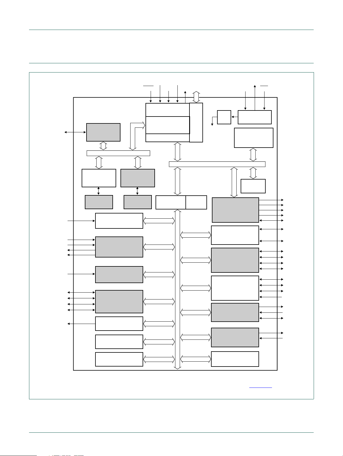
5. Block diagram
UM10114
Chapter 1: Introductory information
Grey-shaded blocks indicate configuration or pinout dependent on part and version number, see Table 1–16.
Fig 1. LPC21xx and LPC22xx block diagram
UM10114_3 © NXP B.V. 2008. All rights reserved.
User manual Rev. 03 — 2 April 2008 11 of 386
Page 12

NXP Semiconductors
UM10114
Chapter 1: Introductory information
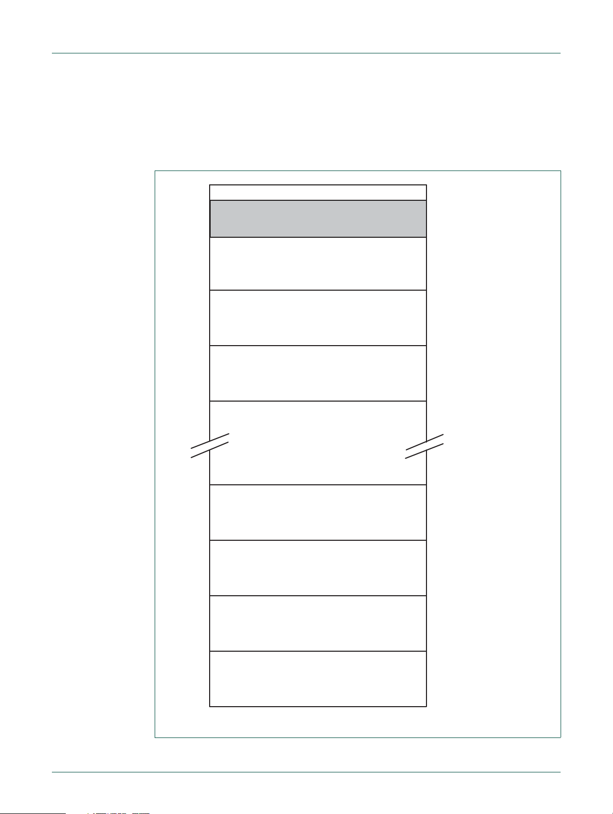
Table 16. LPC21xx/22xx part-specific configuration
Part EMC SRAM Flash Legacy
No-suffix and /00 parts
LPC2109 - 8 kB 64 kB P0/1 - - 1 4/- - LPC2119 - 16 kB 128 kB P0/1 - - 2 4 /- - LPC2129 - 16 kB 256 kB P0/1 - - 2 4 /- - LPC2114 - 16 kB 128 kB P0/1 - - - 4/- - LPC2124 - 16 kB 256 kB P0/1 - - - 4/- - LPC2194 - 16 kB 256 kB P0/1 - - 4 4 /- - LPC2210 yes 16 kB - P0/1/2/3 - - - 4/- - LPC2220 yes 64 kB - P0/1/2/3 P0/1 yes - 8/yes yes yes
LPC2212 yes 16 kB 128 kB P0/1/2/3 - - - 8/- - LPC2214 yes 16 kB 256 kB P0/1/2/3 - - - 8/- - LPC2290 yes 16 kB - P0/1/2/3 - - 2 8/- - LPC2292 yes 16 kB 256 kB P0/1/2/3 - - 2 8/- - LPC2294 yes 16 kB 256 kB P0/1/2/3 - - 4 8/- - -
/01 parts
LPC2109 - 8 kB 64 kB P0/1 P0/1 yes 1 4/yes yes yes
LPC2119 - 16 kB 128 kB P0/1 P0/1 yes 2 4/yes yes yes
LPC2129 - 16 kB 256 kB P0/1 P0/1 yes 2 4/yes yes yes
LPC2114 - 16 kB 128 kB P0/1 P0/1 yes - 4/yes yes yes
LPC2124 - 16 kB 256 kB P0/1 P0/1 yes - 4/yes yes yes
LPC2194 - 16 kB 256 kB P0/1 P0/1 yes 4 4/yes yes yes
LPC2210 yes 16 kB - P0/1/2/3 P0/1 yes - 8/yes yes yes
LPC2212 yes 16 kB 128 kB P0/1/2/3 P0/1 yes - 8/yes yes yes
LPC2214 yes 16 kB 256 kB P0/1/2/3 P0/1 yes - 8/yes yes yes
LPC2290 yes 64 kB - P0/1/2/3 P0/1 yes 2 8/yes yes yes
LPC2292 yes 16 kB 256 kB P0/1/2/3 P0/1 yes 2 8/yes ye s yes
LPC2294 yes 16 kB 256 kB P0/1/2/3 P0/1 yes 4 8/yes ye s yes
GPIO
Fast
GPIO
SSP CAN ADC Enhanced
UART
channels channels/
enhanced
ADC
Enhanced
timers
6. Architectural overview
The LPC21xx/LPC22xx consist of an ARM7TDMI-S CPU with emulation support, the
ARM7 Local Bus for interface to on-chip memory controllers, the AMBA Advanced
High-performance Bus (AHB) for interface to the interrupt controller, and the ARM
Peripheral Bus (APB, a compatible superset of ARM’s AMBA Advanced Peripheral Bus)
for connection to on-chip peripheral functions. The LPC21xx/LPC22xx configures the
ARM7TDMI-S processor in little-endian byte order.
UM10114_3 © NXP B.V. 2008. All rights reserved.
User manual Rev. 03 — 2 April 2008 12 of 386
Page 13

NXP Semiconductors
AHB peripherals are allocated a 2 megabyte range of addresses at the very top of the
4 gigabyte ARM memory space. Each AHB periph eral is allocated a 16 kB address space
within the AHB address space. LPC21xx/LPC22xx peripheral functions (other than the
interrupt controller) are connected to the APB bus. The AHB to APB bridge interfaces the
APB bus to the AHB bus. APB peripherals are also allocated a 2 megabyte range of
addresses, beginning at the 3.5 gigabyte address point. Each APB peripheral is allocated
a 16 kB address space within the APB address space.
The connection of on-chip peripherals to device pins is controlled by a Pin Connect Block
(see Section 8–6
requirements for the use of peripheral functions and pins.
). This must be configured by software to fit specific application
7. ARM7TDMI-S processor
The ARM7TDMI-S is a general purpose 32-bit microprocessor, which offers high
performance and very low power consumption. The ARM architecture is based on
Reduced Instruction Set Computer (RISC) principles, and the instruction set and related
decode mechanism are much simpler than those of microprogrammed Complex
Instruction Set Computers. This simplicity results in a high instruction throughput and
impressive real-time interrupt response from a small and cost-effective processor core.
UM10114
Chapter 1: Introductory information
Pipeline techniques are employed so that all part s of the pro cessing and memory systems
can operate continuously. Typically, while one instruction is being executed, its successor
is being decoded, and a third instruction is being fetched from memory.
The ARM7TDMI-S processor also employs a unique architectural strategy known as
THUMB, which makes it ideally suited to high-volume applications with memory
restrictions, or applications where code density is an issue.
The key idea behind THUMB is that of a super-reduced instruction set. Essentially, the
ARM7TDMI-S processor has two instruction sets:
• The standard 32-bit ARM instruction set.
• A 16-bit THUMB instruction set.
The THUMB set’s 16-bit instruction length allows it to approach twice the density of
standard ARM code while retaining most of the ARM’s performance advantage over a
traditional 16-bit processor using 16-bit registers. This is possible because THUMB code
operates on the same 32-bit register set as ARM code.
THUMB code is able to provide up to 65% of the code size of ARM, and 160% of the
performance of an equivalent ARM processor connected to a 16-bit memory system.
The ARM7TDMI-S processor is described in detail in the ARM7TDMI-S data sh eet that
can be found on official ARM website.
8. On-chip flash memory system
The LPC21xx/LPC22xx incorporate a 64 kB to 256 kB flash memory. This memory may
be used for both code and data storage. Programming of the flash memory may be
accomplished in several ways:
UM10114_3 © NXP B.V. 2008. All rights reserved.
User manual Rev. 03 — 2 April 2008 13 of 386
Page 14

NXP Semiconductors
• using the serial built-in JTAG interface
• using In System Programming (ISP) and UART
• using In Application Programming (IAP) capabilities
The application program, using the IAP functions, may also erase and/or program the
flash while the application is running, allowing a great degree of flexibility for dat a sto rage
field firmware upgrades, etc. The entire flash memory is available for user code because
the boot loader resides in a separate memory location.
The LPC21xx/LPC22xx flash memory provides minimum of 100,000 erase/write cycles
and 20 years of data-retention.
9. On-chip Static RAM (SRAM)
On-chip Static RAM (SRAM) may be used for code and/or data storage. The on-chip
SRAM may be accessed as 8-bits, 16-bits, and 32-bits.
The LPC21xx/LPC22xx SRAM is designed to be accessed as a byte-addressed memory.
Word and halfword accesses to the memory ignore the alignment of the address and
access the naturally-aligned value that is addressed (so a memory access ignores
address bits 0 and 1 for word accesses, and ignores bit 0 for halfword accesses).
Therefore valid reads and writes require data accessed as halfwords to originate from
addresses with address line 0 being 0 (addresses ending with 0, 2, 4, 6, 8, A, C, and E in
hexadecimal notation) and data accessed as words to originate from addresses with
address lines 0 and 1 being 0 (addresses ending with 0, 4, 8, and C in hexadecimal
notation).
UM10114
Chapter 1: Introductory information
The SRAM controller incorporates a write-back buffer in order to prevent CPU stalls
during back-to-back writes. The write-back buffer always holds the last data sent by
software to the SRAM. This data is only written to the SRAM when another write is
requested by software (the data is only written to the SRAM when software does another
write). If a chip reset occurs, actual SRAM contents will not reflect the most recent write
request (i.e. after a "warm" chip reset, the SRAM does not reflect the last wr ite operation).
Any software that checks SRAM contents after reset must take this into account. Two
identical writes to a location guarantee that the data will be present after a Reset.
Alternatively, a dummy write operation before entering idle or power-down mode will
similarly guarantee that the last data written will be present in SRAM after a subsequent
Reset.
UM10114_3 © NXP B.V. 2008. All rights reserved.
User manual Rev. 03 — 2 April 2008 14 of 386
Page 15

UM10114
Chapter 2: LPC21xx/22xx Memory map
Rev. 03 — 2 April 2008 User manual
1. How to read this chapter
Remark: The LPC21xx and LPC22xx contain different memory configurations and
APB/AHB peripherals. See Table 2–17
For an overview of how LPC21xx and LPC22xx parts and versions are described in this
manual, see Section 1–2 “
Table 17. LPC21xx and LPC22xx memory and peripheral configuration
Part EMC
Figure 2–2
addresses size/ addresses size/
No suffix and /01 parts
LPC2109 - 8 kB/
LPC2119 - 16 kB/
LPC2129 - 16 kB/
LPC2114 - 16 kB/
LPC2124 - 16 kB/
LPC2194 - 16 kB/
LPC2210 0x8000 0000 -
0x83FF FFFF
LPC2220 0x8000 0000 -
0x83FF FFFF
LPC2212 0x8000 0000 -
0x83FF FFFF
SRAM
Figure 2–2
0x4000 0000 0x4000 1FFF
0x4000 0000 0x4000 2FFF
0x4000 0000 0x4000 2FFF
0x4000 0000 0x4000 2FFF
0x4000 0000 0x4000 2FFF
0x4000 0000 0x4000 2FFF
16 kB/
0x4000 0000 0x4000 2FFF
64 kB/
0x4001 0000 0x4000 FFFF
16 kB/
0x4000 0000 0x4000 2FFF
How to read this manual”.
Flash
Figure 2–2
addresses
64 kB/
0x0000 0000 0x0000 FFFF
128 kB/
0x0000 0000 0x0001 FFFF
256 kB/
0x0000 0000 0x0003 FFFF
128 kB/
0x0000 0000 0x0001 FFFF
256 kB/
0x0000 0000 0x0003 FFFF
256 kB/
0x0000 0000 0x0003 FFFF
-- --
- 0x3FFF C000 -
128 kB/
0x0000 0000 0x0001 FFFF
for part-specific memory and peripherals.
Fast GPIO
Figure 2–2
addresses APB base addresses
- - 0xE003 8000 -
- - 0xE003 8000 -
- - 0xE003 8000 -
---
---
- - 0xE003 8000 -
0x3FFF FFFF
---
SSP
Table 2–18
0xE005 C000 -
CAN Table 2–18
0xE004 0000
CAN1: 0xE004 4000
0xE004 0000
CAN1:0xE004 4000
CAN2: 0xE004 8000
0xE004 0000
CAN1: 0xE004 4000
CAN2: 0xE004 8000
0xE004 0000
CAN1: 0xE004 4000
CAN2: 0xE004 8000
CAN3: 0xE004 C000
CAN4: 0xE005 0000
UM10114_3 © NXP B.V. 2008. All rights reserved.
User manual Rev. 03 — 2 April 2008 15 of 386
Page 16

NXP Semiconductors
Table 17. LPC21xx and LPC22xx memory and peripheral configuration
Part EMC
Figure 2–2
addresses size/ addresses size/
LPC2214 0x8000 0000 -
0x83FF FFFF
LPC2290 0x8000 0000 -
0x83FF FFFF
LPC2292 0x8000 0000 -
0x83FF FFFF
LPC2294 0x8000 0000 -
0x83FF FFFF
/01 parts
LPC2109 - 8 kB/
LPC2119 - 16 kB/
LPC2129 - 16 kB/
LPC2114 - 16 kB/
LPC2124 - 16 kB/
LPC2194 - 16 kB/
LPC2210 0x8000 0000 -
0x83FF FFFF
LPC2212 0x8000 0000 -
0x83FF FFFF
SRAM
Figure 2–2
16 kB/
0x4000 0000 0x4000 2FFF
16 kB/
0x4000 0000 0x4000 2FFF
16 kB/
0x4000 0000 0x4000 2FFF
16 kB/
0x4000 0000 0x4000 2FFF
0x4000 0000 0x4000 1FFF
0x4000 0000 0x4000 2FFF
0x4000 0000 0x4000 2FFF
0x4000 0000 0x4000 2FFF
0x4000 0000 0x4000 2FFF
0x4000 0000 0x4000 2FFF
16 kB/
0x4000 0000 0x4000 2FFF
16 kB/
0x4000 0000 0x4000 2FFF
Flash
Figure 2–2
addresses
256 kB/
0x0000 0000 0x0003 FFFF
- - - 0xE003 8000 -
256 kB/
0x0000 0000 0x0003 FFFF
256 kB/
0x0000 0000 0x0003 FFFF
64 kB/
0x0000 0000 0x0000 FFFF
128 kB/
0x0000 0000 0x0001 FFFF
256 kB/
0x0000 0000 0x003 FFFF
128 kB/
0x0000 0000 0x0001 FFFF
256 kB/
0x0000 0000 0x003 FFFF
256 kB/
0x0000 0000 0x0003 FFFF
- 0x3FFF C000 -
128 kB/
0x0000 0000 0x0001 FFFF
Fast GPIO
Figure 2–2
addresses APB base addresses
---
- - 0xE003 8000 -
- - 0xE003 8000 -
0x3FFF C000 0x3FFF FFFF
0x3FFF C000 0x3FFF FFFF
0x3FFF C000 0x3FFF FFFF
0x3FFF C000 0x3FFF FFFF
0x3FFF C000 0x3FFF FFFF
0x3FFF C000 0x3FFF FFFF
0x3FFF FFFF
0x3FFF C000 0x3FFF FFFF
UM10114
Chapter 2: LPC21xx/22xx Memory map
SSP
Table 2–18
0xE005 C000 0xE003 8000 -
0xE005 C000 0xE003 8000 -
0xE005 C000 0xE003 8000 -
0xE005 C000 -
0xE005 C000 -
0xE005 C000 0xE003 8000 -
0xE005 C000 -
0xE005 C000 -
CAN Table 2–18
0xE004 0000
CAN1: 0xE004 4000
CAN2: 0xE004 8000
0xE004 0000
CAN1: 0xE004 4000
CAN2: 0xE004 8000
0xE004 0000
CAN1: 0xE004 4000
CAN2: 0xE004 8000
CAN3: 0xE004 C000
CAN4: 0xE005 0000
0xE004 0000
CAN1: 0xE004 4000
0xE004 0000
CAN1: 0xE004 4000
CAN2: 0xE004 8000
0xE004 0000
CAN1: 0xE004 4000
CAN2: 0xE004 8000
0xE004 0000
CAN1: 0xE004 4000
CAN2: 0xE004 8000
CAN3: 0xE004 C000
CAN4: 0xE005 0000
UM10114_3 © NXP B.V. 2008. All rights reserved.
User manual Rev. 03 — 2 April 2008 16 of 386
Page 17

NXP Semiconductors
Table 17. LPC21xx and LPC22xx memory and peripheral configuration
Part EMC
Figure 2–2
addresses size/ addresses size/
LPC2214 0x8000 0000 -
0x83FF FFFF
LPC2290 0x8000 0000 -
0x83FF FFFF
LPC2292 0x8000 0000 -
0x83FF FFFF
LPC2294 0x8000 0000 -
0x83FF FFFF
SRAM
Figure 2–2
16 kB/
0x4000 0000 0x4000 2FFF
64 kB/
0x4001 0000 0x4000 FFFF
16 kB/
0x4000 0000 0x4000 2FFF
16 kB/
0x4000 0000 0x4000 2FFF
Flash
Figure 2–2
addresses
256 kB/
0x0000 0000 0x0003 FFFF
- 0x3FFF C000 -
256 kB/
0x0000 0000 0x0003 FFFF
256 kB/
0x0000 0000 0x0003 FFFF
Fast GPIO
Figure 2–2
addresses APB base addresses
0x3FFF C000 0x3FFF FFFF
0x3FFF FFFF
0x3FFF C000 0x3FFF FFFF
0x3FFF C000 0x3FFF FFFF
UM10114
Chapter 2: LPC21xx/22xx Memory map
SSP
Table 2–18
0xE005 C000 -
0xE005 C000 0xE003 8000 -
0xE005 C000 0xE003 8000 -
0xE005 C000 0xE003 8000 -
CAN Table 2–18
0xE004 0000
CAN1: 0xE004 4000
CAN2: 0xE004 8000
0xE004 0000
CAN1: 0xE004 4000
CAN2: 0xE004 8000
0xE004 0000
CAN1: 0xE004 4000
CAN2: 0xE004 8000
CAN3: 0xE004 C000
CAN4: 0xE005 0000
2. Memory maps
The LPC21xx and LPC22xx incorporate several distinct memory regions, shown in the
following figures. Figure 2–2
user program viewpoint following reset. The interrupt vector area supports address
remapping, which is described later in this section.
shows the overall map of the entire address space from the
UM10114_3 © NXP B.V. 2008. All rights reserved.
User manual Rev. 03 — 2 April 2008 17 of 386
Page 18

NXP Semiconductors
AHB PERIPHERALS
APB PERIPHERALS
RESERVED ADDRESS SPACE
EXTERNAL MEMORY BANKS 0 TO 4
BOOT BLOCK (RE-MAPPED FROM
ON-CHIP FLASH MEMORY)
RESERVED ADDRESS SPACE
UP TO 64 kB ON-CHIP STATIC RAM
FAST GPIO REGISTERS
RESERVED ADDRESS SPACE
UP TO 256 kB ON-CHIP FLASH MEMORY
0xFFFF FFFF
0xF000 0000
0xEFFF FFFF
0xE000 0000
0xC000 0000
0xDFFF FFFF
0x8000 0000
0x7FFF FFFF
0x8400 0000
0x83FF FFFF
0x7FFF E000
0x7FFF DFFF
0x4001 0000
0x4000 FFFF
0x4000 0000
0x3FFF FFFF
0x3FFF C000
0x0004 0000
0x0003 FFFF
4.0 GB
3.75 GB
3.5 GB
3.0 GB
2.0 GB
1.0 GB
0.0 GB
0x0000 0000
UM10114
Chapter 2: LPC21xx/22xx Memory map
Fig 2. LPC21xx and LPC22xx system memory map
UM10114_3 © NXP B.V. 2008. All rights reserved.
User manual Rev. 03 — 2 April 2008 18 of 386
Page 19

NXP Semiconductors
RESERVED
RESERVED
0xF000 0000
0xEFFF FFFF
APB PERIPHERALS
0xE020 0000
0xE01F FFFF
0xE000 0000
AHB PERIPHERALS
0xFFFF FFFF
0xFFE0 0000
0xFFDF FFFF
3.75 GB
3.5 GB
3.5 GB + 2 MB
4.0 GB - 2 MB
4.0 GB
UM10114
Chapter 2: LPC21xx/22xx Memory map
AHB section is 128 x 16 kB blocks (totaling 2 MB).
APB section is 128 x 16 kB blocks (totaling 2MB).
Fig 3. Peripheral memory map
Figures 3 through 4 and Table 2–18 show different views of the peripheral address space.
Both the AHB and APB peripheral areas are 2 megabyte sp aces which are divided up into
128 peripherals. Each peripheral space is 16 kilobytes in size. This allows simplifying the
address decoding for each peripheral. All peripheral register addresses are word aligned
UM10114_3 © NXP B.V. 2008. All rights reserved.
User manual Rev. 03 — 2 April 2008 19 of 386
Page 20
NXP Semiconductors
VECTORED INTERRUPT CONTROLLER
(AHB PERIPHERAL #0)
0xFFFF F000 (4G - 4K)
0xFFFF C000
0xFFFF 8000
(AHB PERIPHERAL #125)
(AHB PERIPHERAL #124)
(AHB PERIPHERAL #3)
(AHB PERIPHERAL #2)
(AHB PERIPHERAL #1)
(AHB PERIPHERAL #126)
0xFFFF 4000
0xFFFF 0000
0xFFE1 0000
0xFFE0 C000
0xFFE0 8000
0xFFE0 4000
0xFFE0 0000
NOT USED
NOT USED
NOT USED
EXTERNAL MEMORY CONTROLLER
NOT USED
NOT USED
(to 32-bit boundaries) regardless of their size. This eliminates the need for byte lane
mapping hardware that would be required to allow byte (8-bit) or half-wor d (16-bit)
accesses to occur at smaller boundaries. An implication of this is that word and half-word
registers must be accessed all at once. For example, it is not possible to read or write the
upper byte of a word register separately.
UM10114
Chapter 2: LPC21xx/22xx Memory map
UM10114_3 © NXP B.V. 2008. All rights reserved.
User manual Rev. 03 — 2 April 2008 20 of 386
Fig 4. AHB peripheral map
Page 21

NXP Semiconductors
Table 18. APB peripheries and base addr esses
APB peripheral Base address Peripheral name
0 0xE000 0000 Watchdog timer
1 0xE000 4000 Timer 0
2 0xE000 8000 Timer 1
3 0xE000 C000 UART0
4 0xE001 0000 UART1
5 0xE001 4000 PWM
6 0xE001 8000 Not used
7 0xE001 C000 I
8 0xE002 0000 SPI0
9 0xE002 4000 RTC
10 0xE002 8000 GPIO
11 0xE002 C000 Pin connect block
12 0xE003 0000 SPI1
13 0xE003 4000 10 bit ADC
14 0xE003 8000 CAN Acceptance Filter RAM
15 0xE003 C000 CAN Acceptance Filter Registers
16 0xE004 0000 CAN Common Registers
17 0xE004 4000 CAN Controller 1
18 0xE004 8000 CAN Controller 2
19 0xE004 C000 CAN Controller 3
20 0xE005 0000 CAN Controller 4
21 - 22 0xE005 4000
23 0xE005 C000 SSP
24 - 126 0xE006 0000 -
127 0xE01F C000 System Control Block
0xE005 8000
0xE01F 8000
2
C
Not used
Not used
UM10114
Chapter 2: LPC21xx/22xx Memory map
3. LPC21xx and LPC22xx memory re-mapping and boot block
3.1 Memory map concepts and operating modes
The basic concept on the LPC21xx and LPC22xx is that each memory area has a
"natural" location in the memory map. This is the address range for which code r esiding in
that area is written. The bulk of each memory space remains permanently fixed in the
same location, eliminating the need to have portions of the code designed to run in
different address ranges.
Because of the location of the interrupt vectors on the ARM7 processor (at addresses
0x0000 0000 through 0x0000 001C, as shown in Table 2–19
Boot Block and SRAM spaces need to be re-mapped in order to allow alternative uses of
interrupts in the different operating modes described in Table 2–20
interrupts is accomplished via the Memory Mapping Control features. To select a specific
memory mapping mode, see Table 6–62
UM10114_3 © NXP B.V. 2008. All rights reserved.
User manual Rev. 03 — 2 April 2008 21 of 386
.
below), a small portion of the
. Re-mapping of the
Page 22

NXP Semiconductors
Table 19. ARM exception vector locations
Address Exception
0x0000 0000 Reset
0x0000 0004 Undefined Instruction
0x0000 0008 Software Interrupt
0x0000 000C Prefetch Abort (instruction fetch memory fault)
0x0000 0010 Data Abort (data access memory fault)
0x0000 0014 Reserved
0x0000 0018 IRQ
0x0000 001C FIQ
Table 20. LPC21xx and LPC22xx memory mapping modes
Mode Activation Usage
Boot
Loader
mode
User
Flash
mode
User RAM
mode
User
External
mode
Hardware
activation by
any Reset
Software
activation by
Boot code
Software
activation by
User program
Activated by
BOOT1:0
pins
UM10114
Chapter 2: LPC21xx/22xx Memory map
Note: Identified as reserved in ARM documentation.
The boot loader always executes after any reset. The boot block
interrupt vectors are mapped to the bottom of memory to allow
handling exceptions and using interrupts during the boot loading
process.
Activated by boot loader when a valid user program signature is
recognized in memory and boot loader operation is not forced.
Interrupt vectors are not re-mapped and are found in the bottom of the
flash memory.
Remark: This mode is not available in flashless parts (see
Table 2–17
Activated by a user program as desired. Interrupt vectors are
re-mapped to the bottom of the Static RAM.
Activated by the boot loader when one or both BOOT pins are LOW at
the end of RESET LOW. Interrupt vectors are re-mapped from the
bottom of the external memory map (see Section 8–6.5
Remark: This mode is available for parts with external memory
controller only (see Table 2–17
).
).
).
3.2 Memory re-mapping
In order to allow for compatibility with future derivatives, the entire boot block is mapped to
the top of the on-chip memory space. Memory spaces other tha n th e int er ru pt vecto r s
remain in fixed locations. Figure 2–5
defined above.
The portion of memory that is re-mapped to allow interrupt processing in different modes
includes the interrupt vector area (32 bytes) and an additional 32 bytes, for a total of
64 bytes. The re-mapped code locations overlay addresses 0x0000 0000 through
0x0000 003F. The vector contained in the SRAM, external memory, and boot block must
contain branches to the actual interrupt handlers or to other instructions that accomplish
the branch to the interrupt handlers.
There are two reasons this configuration was chosen:
UM10114_3 © NXP B.V. 2008. All rights reserved.
User manual Rev. 03 — 2 April 2008 22 of 386
shows the on-chip memory mapping in the modes
Page 23

NXP Semiconductors
8 kB BOOT BLOCK
ON-CHIP FLASH MEMORY
0.0 GB
ACTIVE INTERRUPT VECTORS
FROM BOOT BLOCK
0x7FFF FFFF
2.0 GB - 8 kB
2.0 GB
(BOOT BLOCK INTERRUPT VECTORS)
0x0000 0000
0x7FFF E000
(SRAM INTERRUPT VECTORS)
ON-CHIP SRAM
RESERVED ADDRESS SPACE
1.0 GB
0x4000 0000
RESERVED ADDRESS SPACE
0x4003 FFFF
0x4000 4000
1. Minimize the need for the SRAM and Boot Block vectors to deal with arbitrary
2. To provide space to store constants for jumping beyond the range of single word
Re-mapped memory areas, including the boot block and interrupt vectors, continue to
appear in their original location in addition to the re-mapped address.
UM10114
Chapter 2: LPC21xx/22xx Memory map
boundaries in the middle of code space.
branch instructions.
Details on re-mapping and examples can be found in Section 6–8.1 “
control register (MEMMAP - 0xE01F C040)” on page 68.
Memory Mapping
Fig 5. Map of lower memory is showing re-mapped and re-mappable areas for a part
with on-chip flash memory
4. Prefetch Abort and Data Abort Exceptions
The LPC21xx and LPC22xx generate the appropriate bus cycle abort exception if an
access is attempted for an address that is in a reserved or unassigned address region.
The regions are:
• Areas of the memory map that are not implemented for a specific ARM derivative. Fo r
the LPC21xx and LPC22xx, those areas are:
– Address space between the on-chip non-volatile memory and On-Chip SRAM,
labelled "Reserved Address Space" in Figure 2–2
address range from 0x0002 0000 to 0x3FFF FFFF for the 128 kB flash device and
0x0004 0000 to 0x3FFF FFFF for the 256 kB flash device.
– Address space between on-chip SRAM and the boot block. This is the address
UM10114_3 © NXP B.V. 2008. All rights reserved.
User manual Rev. 03 — 2 April 2008 23 of 386
range from 0x4000 4000 to 0x7FFF DFFF, labelled "Reserved Address Space" in
Figure 2–2
, and Figure 2–5.
, and Figure 2–5. This is an
Page 24

NXP Semiconductors
• Unassigned AHB peripheral spaces. See Figure 2–4.
• Unassigned APB peripheral spaces. See Table 2–18.
For these areas, both attempted data acce ss and in struction fetch genera te an exception.
In addition, a Prefetch Abort exception is generated for any instruction fetch that maps to
an AHB or APB peripheral address.
Within the address space of an existing APB peripheral, a data abort exception is not
generated in response to an access to an undefined address. Address decoding within
each peripheral is limited to that needed to distinguish defined registers within the
peripheral itself. For example, an access to address 0xE000 D000 (an undefined address
within the UART0 space) may result in an access to the register defined at address
0xE000 C000. Details of such address aliasing within a peripheral space are not defined
in the LPC21xx and LPC22xx documentation and are not a su pp or te d fe at ur e.
UM10114
Chapter 2: LPC21xx/22xx Memory map
– Address space between the top of the boot block and the APB peripheral space,
except space used for external memory (LPC2292/2294 only). This is the address
range from 0x8000 0000 to 0xDFFF FFFF, labelled "Reserved Address Space" in
Figure 2–2
– Reserved regions of the AHB and APB spaces. See Figure 2–3
, and Figure 2–5.
and Table 2–18.
Note: The ARM core stores the Prefetch Abort flag along with the associated instruction
(which will be meaningless) in the pipeline and processes the abort only if an attempt is
made to execute the instruction fetched from the illegal address. This prevents accidental
aborts that could be caused by prefetches that occur when code is executed very near a
memory boundary.
UM10114_3 © NXP B.V. 2008. All rights reserved.
User manual Rev. 03 — 2 April 2008 24 of 386
Page 25

UM10114
Chapter 3: LPC21xx/22xx Memory Accelerator Module (MAM)
Rev. 03 — 2 April 2008 User manual
1. How to read this chapter
The MAM is identical for all parts with flash memory. It is available in the following parts:
• LPC2109, LPC2119, LPC2129, and /01 versions
• LPC2114, LPC2124, and /01 versions
• LPC2194 and LPC2194/01
• LPC2212, LPC2214, and /01 versions
• LPC2292, LPC2294, and /01 versions
For an overview of how LPC21xx and LPC22xx parts and versions are described in this
manual, see Section 1–2 “
How to read this manual”.
2. Introduction
3. Operation
The MAM block in the LPC21xx and LPC22xx maximizes the performance of the ARM
processor when it is running code in flash memory using a dual flash bank.
Simply put, the Memory Accelerator Module (MAM) attempts to have the next ARM
instruction that will be needed in its latches in time to prevent CPU fetch stalls. The
method used is to split the flash memory into two banks, each capable of independent
accesses. Each of the two flash banks has its own prefetch buffer a nd branch trail buffer.
The branch trail buffers for the two banks capture two 128-bit lines of flash data when an
instruction fetch is not satisfied by either the pref etc h bu ffer or branch trail bu ffer for its
bank, and for which a prefetch has not been initia te d. Each pr e fet ch buffer captu res one
128-bit line of instructions from its flash bank at the conclusion of a prefetch cycle initiated
speculatively by the MAM.
Each 128 bit value includes four 32-bit ARM instructions or eight 16-bit Thumb
instructions. During sequential code execution, typically one flash bank contains or is
fetching the current instruction and the entir e flash line that contains it. The other bank
contains or is prefetching the next sequential code line. After a code line delivers its last
instruction, the bank that contained it begins to fetch the next line in that bank.
Timing of flash read operations is programmable and is described in Section 3–9
.
Branches and other program flow changes cause a break in the sequential flow of
instruction fetches described above. When a backward branch occurs, there is a distinct
possibility that a loop is being executed. In this case the branch trail buffers may already
contain the target instruction. If so, execution continues without the need for a flash read
cycle. For a forward branch, there is also a chance that the new address is already
contained in one of the prefetch buffers. If it is, the branch is again taken with no delay.
UM10114_3 © NXP B.V. 2008. All rights reserved.
User manual Rev. 03 — 2 April 2008 25 of 386
Page 26

NXP Semiconductors
When a branch outside the contents of the branch trail and prefetch buffers is taken, one
flash access cycle is needed to load the branch trail buffers. Subsequently, there will
typically be no further fetch delays until another such “Instruction Miss” occurs.
The flash memory controller detects data accesses to the flash memo ry and uses a
separate buffer to store the results in a manner similar to that used during code fetches.
This allows faster access to data if it is accessed sequentially. A single line buffer is
provided for data accesses, as opposed to the two buf fers per flash bank tha t are provided
for code accesses. There is no prefetch function for data accesses.
4. MAM blocks
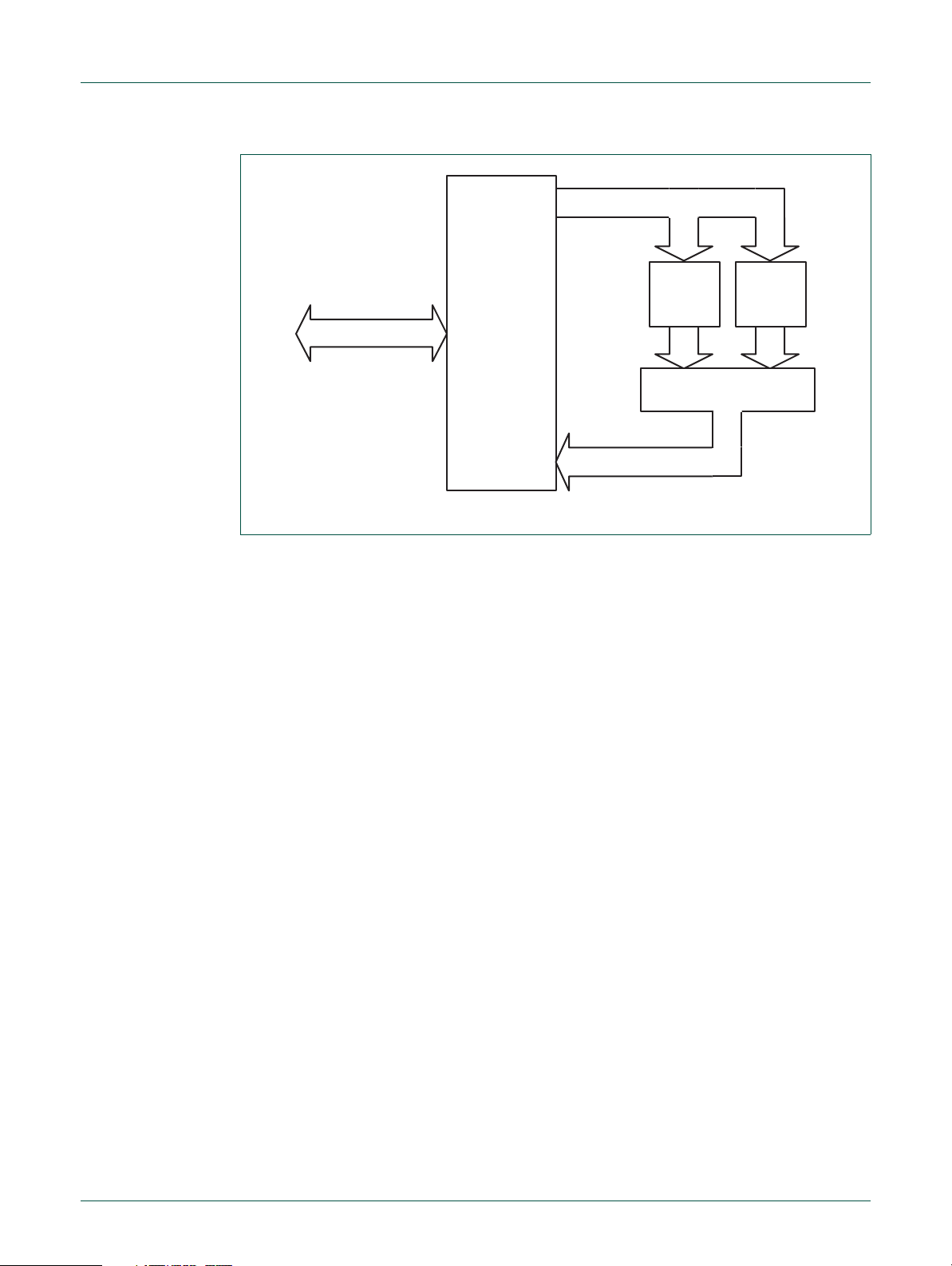
The Memory Accelerator Module is divided into several functional blocks:
• A flash address latch for each bank: An incrementor function is associated with the
• Two flash memory banks
• Instruction latches, data latches, address comparison latches
• Control and wait logic
UM10114
Chapter 3: LPC21xx/22xx Memory Accelerator Module (MAM)
bank 0 flash address latch.
Figure 3–6
paths.
In the following descriptions, the term “fetch” applies to an explicit flash read request from
the ARM. “Pre-fetch” is used to denote a flash read of instructions beyond the current
processor fetch address.
shows a simplified block diagram of the Memory Accelerator Module dat a
4.1 Flash memory bank
There are two banks of flash memory in order to allow parallel access and eliminate
delays for sequential access.
Flash programming operations are not controlled by the MAM but are handled as a
separate function. A “boot block” sector contains flash programming algorithms that may
be called as part of the application program and a loader that may be run to allow serial
programming of the flash memory.
The flash memories are wired so that each sector exists in both banks and that a sector
erase operation acts on part of both banks simultaneously. In effect, the existence of two
banks is transparent to the programming functions.
UM10114_3 © NXP B.V. 2008. All rights reserved.
User manual Rev. 03 — 2 April 2008 26 of 386
Page 27
NXP Semiconductors
ARM LOCAL BUS
BUS
INTERFACE
FLASH
MEMORY
BANK 0
FLASH
MEMORY
BANK 1
BANK SELECTION
MEMORY DATA
Fig 6. Simplified block diagram of the Memory Accelerator Module (MAM)
UM10114
Chapter 3: LPC21xx/22xx Memory Accelerator Module (MAM)
4.2 Instruction latches and data latches
Code and data accesses are treated separately by the Memory Accelerator Mod ule.There
are two sets of 128-bit instruction latches and 12-bit compar ison address latches
associated with each flash bank. One of the two sets, called the branch trail buffer, holds
the data and comparison address for that bank from the last instruction miss. The other
set, called the prefetch buffer, holds the data and comparison address from prefetches
undertaken speculatively by the MAM. Each instruction latch ho lds 4 words of code (4
ARM instructions, or 8 Thumb instructions).
Similarly, there is a 128-bit data latch and 13-bit data address latch, that are used during
data cycles. This single set of latches is shared by both flash bank s. Each data access
that is not in the data latch causes a flash fetch of 4 words of data, which are captured in
the data latch. This speeds up sequential data operations, but has little or no effect on
random accesses.
4.3 Flash programming Issues
Since the flash memory does not allow access during programming and erase operations,
it is necessary for the MAM to force the CPU to wait if a memory access to a flash address
is requested while the flash module is busy . Un der some conditions, this delay could result
in a Watchdog time-out. The user will need to be aware of this possibility and take step s to
insure that an unwanted Watchdog reset does not cause a system failure while
programming or erasing the flash memory.
UM10114_3 © NXP B.V. 2008. All rights reserved.
User manual Rev. 03 — 2 April 2008 27 of 386
In order to preclude the possibility of stale data being read from the flash memory, the
LPC21xx and LPC22xx MAM holding latches are automatically invalidated at the
beginning of any flash programming or erase opera tion. Any subsequent read from a flash
address will cause a new fetch to be initiated after the flash operation has completed.
Page 28

NXP Semiconductors
5. MAM operating modes
Three modes of operation are defined for the MAM, trading off performance for ease of
predictability:
Mode 0: MAM off. All memory requests result in a flash read operation (see Table
note 3–2). There are no instruction prefetches.
Mode 1: MAM partially enabled. Sequential instruction accesses are fulfilled from the
holding latches if the data is present. Instruction prefetch is enabled. Non-sequential
instruction accesses initiate flash read operations (see Table note 3–2
all branches cause memory fetches. All data operations cause a flash read because
buffered data access timing is hard to predict and is very situation dependent.
Mode 2: MAM fully enabled. Any memory request (code or data) for a value that is
contained in one of the corresponding holding latches is fulfilled from the latch.
Instruction prefetch is enabled. Flash read operations are initiated for instruction
prefetch and code or data values not available in the corresponding holding latches.
T able 21. MAM responses to program accesses of various types
Program Memory Request Type MAM Mode
Sequential access, data in latches Initiate Fetch
Sequential access, data not in latches Initiate Fetch Initiate Fetch
Non-sequential access, data in latches Initiate Fetch
Non-sequential access, data not in latches Initiate Fetch Initiate Fetch
UM10114
Chapter 3: LPC21xx/22xx Memory Accelerator Module (MAM)
). This means that
0 1 2
[2]
Use Latched
Data
[2]
Initiate Fetch
[1]
Use Latched
Data
[1]
Initiate Fetch
[1][2]
Use Latched
Data
[1]
Initiate Fetch
[1]
[1]
[1]
[1]
[1] Instruction prefetch is enabled in modes 1 and 2.
[2] The MAM actually uses latched data if it is available, but mimics the timing of a flash read operation. This
saves power while resulting in the same execution timing. The MAM can truly be turned off by setting the
fetch timing value in MAMTIM to one clock.
Table 22. MAM responses to data accesses of various types
Data Memory Request T ype MAM Mode
0 1 2
Sequential access, data in latches Initiate Fetch
[1]
Initiate Fetch
[1]
Use Latched
Data
Sequential access, data not in latches Initiate Fetch Initiate Fetch Initiate Fetch
Non-sequential access, data in latches Initiate Fetch
[1]
Initiate Fetch
[1]
Use Latched
Data
Non-sequential access, data not in latches Initiate Fetch Initiate Fetch Initiate Fetch
[1] The MAM actually uses latched data if it is available, but mimics the timing of a flash read operation. This
saves power while resulting in the same execution timing. The MAM can truly be turned off by setting the
fetch timing value in MAMTIM to one clock.
UM10114_3 © NXP B.V. 2008. All rights reserved.
User manual Rev. 03 — 2 April 2008 28 of 386
Page 29

NXP Semiconductors
6. MAM configuration
After reset the MAM defaults to the disabled state. Software can turn memory access
acceleration on or off at any time. This allows most of an application to be run at the
highest possible performance, while certain functions can be run at a somewhat slower
but more predictable rate if more precise timing is required.
7. Register description
All registers, regardless of size, are on word address boundaries. Details of the registers
appear in the description of each function.
T able 23. Summary of MAM registers
Name Description Access Reset
MAMCR Memory Accelerator Module Control Register.
Determines the MAM functional mode, that is, to
what extent the MAM performance enhancements
are enabled. See Table 3–24
MAMTIM Memory Accelerator Module Timing control.
Determines the number of clocks used for flash
memory fetches (1 to 7 processor clocks).
UM10114
Chapter 3: LPC21xx/22xx Memory Accelerator Module (MAM)
Address
[1]
value
R/W 0x0 0xE01F C000
.
R/W 0x07 0xE01F C004
[1] Reset value reflects the data stored in used bits only. It does not include reserved bits content.
8. MAM Control Register (MAMCR - 0xE01F C000)
Two configuration bits select the three MAM operating modes, as shown in Table 3–24.
Following Reset, MAM functions are disabled. Changing the MAM operating mode causes
the MAM to invalidate all of the holding latches, resulting in new reads of flash information
as required.
T able 24. MAM Control Register (MAMCR - address 0xE01F C000) bit description
Bit Symbol Value Description Reset
1:0 MAM_mode
_control
7:2 - - Reserved, user software should not write ones to reserved
00 MAM functions disabled 0
01 MAM functions partially enabled
10 MAM functions fully enabled
11 Reserved. Not to be used in the ap plication.
bits. The value read from a reserved bit is not defined.
9. MAM Timing register (MAMTIM - 0xE01F C004)
The MAM Timing register determines how many CCLK cycles are used to access the
flash memory . This allows tuning MAM timin g to match the processor operating frequency.
flash access times from 1 clock to 7 clocks are possible. Single clock flash accesses
would essentially remove the MAM from timing calculations. In this case the MAM mode
may be selected to optimize power usage.
value
NA
UM10114_3 © NXP B.V. 2008. All rights reserved.
User manual Rev. 03 — 2 April 2008 29 of 386
Page 30

NXP Semiconductors
T able 25. MAM Timing register (MAMTIM - address 0xE01F C004) bit description
Bit Symbol Value Description Reset
2:0 MAM_fetch_
7:3 - - Reserved, user software should not write ones to reserved
UM10114
Chapter 3: LPC21xx/22xx Memory Accelerator Module (MAM)
value
000 0 - Reserved. 07
cycle_timing
001 1 - MAM fetch cycles are 1 processor clock (CCLK) in
duration
010 2 - MAM fetch cycles are 2 CCLKs in duration
011 3 - MAM fetch cycles are 3 CCLKs in duration
100 4 - MAM fetch cycles are 4 CCLKs in duration
101 5 - MAM fetch cycles are 5 CCLKs in duration
110 6 - MAM fetch cycles are 6 CCLKs in duration
111 7 - MAM fetch cycles are 7 CCLKs in duration
Warning: These bits set the duration of MAM flash fetch operations
as listed here. Improper setting of this value may result in incorrect
operation of the device.
NA
bits. The value read from a reserved bit is not defined.
10. MAM usage notes
When changing MAM timing, the MAM must first be turned off by writing a zero to
MAMCR. A new value may then be written to MAMTIM. Finally, the MAM may be turned
on again by writing a value (1 or 2) corresponding to the desired operating mode to
MAMCR.
For system clock slower than 20 MHz, MAMTIM can be 001. For system clock between
20 MHz and 40 MHz, flash access time is suggested to be 2 CCLKs, while in systems with
system clock faster than 40 MHz, 3 CCLKs are proposed. For system clocks of 60 MHz
and above, 4CCLK’s are needed.
Table 26. Suggestions for MAM timing selection
system clock Number of MAM fetch cycles in MAMTIM
< 20 MHz 1 CCLK
20 MHz to 40 MHz 2 CCLK
40 MHz to 60 MHz 3 CCLK
> 60 MHz 4 CCLK
UM10114_3 © NXP B.V. 2008. All rights reserved.
User manual Rev. 03 — 2 April 2008 30 of 386
Page 31

UM10114
Chapter 4: LPC21xx/22xx External Memory Controller (EMC)
Rev. 03 — 2 April 2008 User manual
1. How to read this chapter
This chapter applies to all parts with external memory controller. The EMC is identical for
all these parts. It is available in the following parts (in all 144 pin packages):
• LPC2210, LPC2210/01, and LPC22 2 0
• LPC2212, LPC2214, and /01 versions
• LPC2290 and LPC2290/01
• LPC2292, LPC2294, and /01 versions
The LPC21xx parts do not have an EMC controller.
For an overview of how LPC21xx and LPC22xx parts and versions are described in this
manual, see Section 1–2 “
How to read this manual”.
2. Features
3. Description
• Support for various static memory-mapped devices including RAM, ROM, flash, burst
ROM, and some external I/O devices
• Asynchronous page mode read operation in non-clocked memory subsystems
• Asynchronous burst mode read access to burst mode ROM devices
• Independent configuration for up to four banks, each up to 16 MB
• Programmable bus turnaround (idle) cycles (1 to 16)
• Programmable read and write WAIT states (up to 32) for static RAM devices
• Programmable initial and subsequent burst read WAIT state, for burst ROM devices
• Programmable write protection
• Programmable burst mode operation
• Programmable read byte lane enable control
The external Static Memory Controller is an AMBA AHB slave module which provides an
interface between an AMBA AHB system bus and external (off-chip) memory devices. It
provides support for up to four independently configurable memory banks simult aneously.
Each memory bank is capable of supporting SRAM, ROM, Flash EPROM, Burst ROM
memory, or some external I/O devices .
Each memory bank may be 8, 16, or 32 bits wide.
Since the LPC22xx 144 pin packages pin out address lines A[23:0] only, the decoding
among the four banks uses address bits A[25:24]. The native lo catio n of th e four ban ks is
at the start of the External Memory area identified in Figure 2–2
for initial booting under control of the state of the BOOT[1:0] pins.
UM10114_3 © NXP B.V. 2008. All rights reserved.
User manual Rev. 03 — 2 April 2008 31 of 386
, but Bank 0 can be used
Page 32

NXP Semiconductors
Table 27. Address ranges of the external memory banks
Bank Address range Configuration register
0 0x8000 0000 - 0x80FF FFFF BCFG0
1 0x8100 0000 - 0x81FF FFFF BCFG1
2 0x8200 0000 - 0x82FF FFFF BCFG2
3 0x8300 0000 - 0x83FF FFFF BCFG3
4. Pin description
Table 28. External Memory Controller pin description
Pin name Type Pin description
D[31:0] Input/Output External memory Data lines
A[23:0] Output External memory Address lines
OE Output Low-active Output Enable signal
BLS[3:0] Output Low-active Byte Lane Select signals
WE Output Low-active Write Enable signal
CS[3:0] Output Low-active Chip-Select signals
UM10114
Chapter 4: LPC21xx/22xx External Memory Controller (EMC)
5. Register description
The external memory controller contains 4 registers as shown in Table 4–29.
Table 29. External Memory Controller register map
Name Description Access Reset value,
BCFG0 Configuration register for memory bank 0 R/W 0x0000 FBEF 0xFFE0 0000
BCFG1 Configuration register for memory bank 1 R/W 0x2000 FBEF 0xFFE0 0004
BCFG2 Configuration register for memory bank 2 R/W 0x1000 FBEF 0xFFE0 0008
BCFG3 Configuration register for memory bank 3 R/W 0x0000 FBEF 0xFFE0 000C
Each register selects the following options for its memory bank:
• The number of idle clock cycles inserted between read and write accesses in this
bank, and between an access in another bank and an access in this bank, to avoid
bus contention between devices (1 to 17 clocks)
• The length of read accesses, except for subsequent reads from a burst ROM (3 to 35
clocks)
• The length of write accesses (3 to 19 clocks)
• Whether the bank is write-protected or not
• Whether the bank is 8, 16, or 32 bits wide
Address
see Table 4–30
UM10114_3 © NXP B.V. 2008. All rights reserved.
User manual Rev. 03 — 2 April 2008 32 of 386
Page 33

NXP Semiconductors
5.1 Bank Configuration Registers 0-3 (BCFG0-3 - 0xFFE0 0000 to 0xFFE0 000C)
Table 30. Bank Configuration Registers 0-3 (BCFG0-3 - 0xFFE0 0000 to 0xFFE0 000C)
BCFG0-3 Name Function Reset
3:0 IDCY This field controls the minimum number of “idle” CCLK cycles
4 - Reserved, user software should not write ones to reserved bits.
9:5 WST1 This field controls the length of read accesses (except for
10 RBLE This bit should be 0 for banks composed of byte-wide or
15:11 WST2 For SRAM banks, this field controls the length of write accesses,
23:16 - Reserved, user software should not write ones to reserved bits.
24 BUSERR The only known case in which this bit is set is if the EMC detects
25 WPERR This bit is set if software attempts to write to a bank that has the
26 WP A 1 in this bit write-protects the bank. 0
27 BM A 1 in this bit id entifies a burst-ROM bank. 0
29:28 MW Th is field controls the width of the data bus for this bank:
31:30 AT Always write 00 to this field. 00
Chapter 4: LPC21xx/22xx External Memory Controller (EMC)
address description
that the EMC maintains between read and write accesses in this
bank, and between an access in another bank and an access in
this bank, to avoid bus contention between devices. The number
of idle CCLK cycles between such accesses is the value in this
field plus 1.
The value read from a reserved bit is not defined.
subsequent reads from a burst ROM). The length of read
accesses, in CCLK cycles, is this field value plus 3.
non-byte-partitioned devices, so that the EMC drives the BLS3:0
lines High during read accesses. This bit should be 1 for banks
composed of 16-bit and 32-bit wide devices that include byte
select inputs, so that the EMC drives the BLS3:0 lines Low
during read accesses.
which consist of:
One CCLK cycle of address setup with CS, BLS, and WE high
This value plus 1, CCLK cycles with address valid and CS, BLS,
and WE low
AND
One CCLK cycle with address valid, CS low, BLS and WE high.
For burst ROM banks, this field controls the length of subsequent
accesses, which are (this value plus 1) CCLK cycles long.
The value read from a reserved bit is not defined.
an AMBA request for more than 32 bits of data. The
ARM7TDMI-S will not make such a request.
WP bit 1. Write a 1 to this bit to clear it.
00=8 bit, 01=16 bit, 10=32 bit, 11=reserved
UM10114
value
1111
NA
11111
0
11111
NA
0
0
See
Table 4–
31
The table below shows the state of BCFG0[29:28] after the Boot Loader has run. The
hardware reset state of these bits is 10.
UM10114_3 © NXP B.V. 2008. All rights reserved.
User manual Rev. 03 — 2 April 2008 33 of 386
Page 34

NXP Semiconductors
T able 31. Default memory widths at reset
Bank BOOT[1:0] during Reset BCFG[29:28] Reset value Memory width
0LL 00 8bits
0LH 01 16bits
0HL 10 32bits
0HH 01 16bits
1XX 10 32bits
2XX 01 16bits
3XX 00 8bits
5.2 Read Byte Lane Control (RBLE)
The External Memory Controller (EMC) generates byte lane control signals BLS[3:0]
according to:
• External memory bank data bus wid th , de fined within each configuration register (see
• External memory bank type, being either byte (8 bits), halfword (16 bits) or word (32
UM10114
Chapter 4: LPC21xx/22xx External Memory Controller (EMC)
MW field in BCFG register)
bits) (see RBLE field in BCFG register)
Each memory bank can either be 8, 16 or 32 bits wide. The type of memory used to
configure a particular memory bank determines how the WE and BLS signals are
connected to provide byte, halfword and word access. For read accesses, it is necessary
to control the BLS signals by driving them either all HIGH, or all LOW.
This control is achieved by programming the Read Byte Lane Enable (RBLE) bit within
each configuration register. The following two sections explain why different connections
in respect of WE and BLS[3:0] are needed for different memory configurations.
5.2.1 Accesses to memory banks constructed from 8-bit or non byte-partitioned
memory devices
For memory banks constructed from 8-bit or non byte-partitioned memory devices, it is
important that the RBLE bit is cleared to zero within the respective memory bank
configuration register. This forces all BLS[3:0] lines HIGH during a read access to that
particular bank.
Figure 4–7
memory banks that are 8, 16 and 32 bits wide. In each of these configurations, the
BLS[3:0] signals are connected to write enable (WE) inputs of each 8-bit memory.
Note: The WE signal from the EMC is not used. For write transfers, the relevant BLS[3:0]
byte lane signals are asserted LOW and steer the data to the addressed bytes.
For read transfers, all of the BLS[3:0] lines are deasserted HIGH, which allows the
external bus to be defined for at least the width of the accessed memory.
(a), Figure 4–8 (a) and Figure 4–9 show 8-bit memory being used to configure
UM10114_3 © NXP B.V. 2008. All rights reserved.
User manual Rev. 03 — 2 April 2008 34 of 386
Page 35

NXP Semiconductors
5.2.2 Accesses to memory banks constructed from 16 or 32 bit memory devices
For memory banks constructed from 16 bit or 32-bit memory devices, it is important that
the RBLE bit is set to one within the respective memory bank configuraton register. This
asserts all BLS[3:0] lines LOW during a read access to that particular bank. For 16 and
32-bit wide memory devices, byte select signals exist and must be appropriately
controlled as shown in Figure 4–7
6. External memory interface
External memory interfacing depends on the bank width (32, 16 or 8 bit selected via MW
bits in corresponding BCFG register). Furthermore, the memory chip(s) require an
adequate setup of RBLE bit in BCFG register. Memory accessed with an 8-bit wide data
bus require RBLE = 0, while memory banks capable of accepting 16 or 32 bit wide data
require RBLE = 1.
If a memory bank is configured to be 32 bits wide, address lines A0 and A1 can be used
as non-address lines. If a memory bank is configured to 16 bits wide, A0 is not required.
However, 8 bit wide memory banks do require all address lines down to A0. Configuring
A1 and/or A0 line(s) to provide address or non-address function is accomplished using
bits 23 and 24 in Pin Function Select Register 2 (PINSEL2 register, see Table 8–88
UM10114
Chapter 4: LPC21xx/22xx External Memory Controller (EMC)
and Figure 4–8.
).
Symbol "a_b" in the following figures refers to the highest order address line in the data
bus. Symbol "a_m" refers to the highest order address line of the me mory chip used in the
external memory interface.
See Section 8–6.5 “
Boot control for LPC22xx part s ” for how to boot from external memor y.
UM10114_3 © NXP B.V. 2008. All rights reserved.
User manual Rev. 03 — 2 April 2008 35 of 386
Page 36

NXP Semiconductors
A[a_b:2]
BLS[1]
D[15:8]
CE
OE
WE
IO[7:0]
A[a_m:0]
BLS[0]
D[7:0]
CE
OE
WE
IO[7:0]
A[a_m:0]
OE
CS
BLS[3]
D[31:24]
CE
OE
WE
IO[7:0]
A[a_m:0]
BLS[2]
D[23:16]
CE
OE
WE
IO[7:0]
A[a_m:0]
OE
CS
WE
CE
OE
WE
UB
LB
IO[15:0]
A[a_m:0]
D[31:16]
BLS[2]
CE
OE
WE
UB
LB
IO[15:0]
A[a_m:0]
D[15:0]
BLS[0]
A[a_b:2]
BLS[3] BLS[1]
OE
CS
WE
CE
OE
WE
B3
B2
B1
B0
IO[31:0]
A[a_m:0]
D[31:0]
BLS[2]
A[a_b:2]
BLS[3]
BLS[0]
BLS[1]
Chapter 4: LPC21xx/22xx External Memory Controller (EMC)
a. 32 bit wide memory bank interfaced to 8 bit memory chips (RBLE = 0)
UM10114
b. 32 bit wide memory bank interfaced to 16 bit memory chips (RBLE = 1)
c. 32 bit wide memory bank interfaced to 32 bit memory chips (RBLE = 1)
Fig 7. 32 bit bank external memory interfaces (BGFGx Bits MW = 10)
UM10114_3 © NXP B.V. 2008. All rights reserved.
User manual Rev. 03 — 2 April 2008 36 of 386
Page 37

NXP Semiconductors
OE
CS
BLS[1]
D[15:8]
CE
OE
WE
IO[7:0]
A[a_m:0]
BLS[0]
D[7:0]
CE
OE
WE
IO[7:0]
A[a_m:0]
A[a_b:1]
OE
CS
WE
CE
OE
WE
UB
LB
IO[15:0]
A[a_m:0]
D[15:0]
BLS[0]
A[a_b:1]
BLS[1]
OE
CS
BLS[0]
D[7:0]
CE
OE
WE
IO[7:0]
A[a_m:0]
A[a_b:0]
Chapter 4: LPC21xx/22xx External Memory Controller (EMC)
a. 16 bit wide memory bank interfaced to 8 bit memory chips (RBLE = 0)
UM10114
b. 16 bit wide memory bank interfaced to 16 bit memory chips (RBLE = 1)
Fig 8. 16 bit bank external memory interfaces (BCFGx bits MW = 01)
Fig 9. 8 bit bank external memory interface (BCFGx bits MW = 00 and RBLE = 0)
7. Typical bus sequences
The following figures show typical external read and write access cycles. XCLK is the
clock signal available on P3.23. While not necessarily used by external memory, in these
examples it is used to provide time reference (XCLK and CCLK are set to have the same
UM10114_3 © NXP B.V. 2008. All rights reserved.
User manual Rev. 03 — 2 April 2008 37 of 386
frequency).
Page 38

NXP Semiconductors
WE/BLS
XCLK
CS
addr
data
OE
WE/BLS
change valid data
valid address
1 wait state
(WST1=0)
XCLK
CS
addr
data
OE
change valid data
valid address
2 wait states
(WST1=1)
XCLK
CS
addr
data
OE
WE/BLS
valid address
valid data
XCLK
CS
addr
data
OE
WE/BLS
valid address
valid data
WST2 = 0
WST2 = 1
UM10114
Chapter 4: LPC21xx/22xx External Memory Controller (EMC)
Fig 10. External memory read access (WST1 = 0 and WST1 = 1 examples)
Fig 11. External memory write access (WST2 = 0 and WST2 = 1 examples)
Figure 4–10 and Figure 4–11 show typical read and write accesses to external memory.
Dashed lines on Figure 4–10
having BLS lines connected to UB/LB or B[3:0] (see Section 4–5.2.2
Figure 4–8
It is important to notice that some variations from Figure 4–10
).
correspond to memory banks using 16/32 bit memory chips
and Figure 4–7 ,
and Figure 4–11 do exist in
some particular cases.
UM10114_3 © NXP B.V. 2008. All rights reserved.
User manual Rev. 03 — 2 April 2008 38 of 386
Page 39

NXP Semiconductors
Address A Ad.A+1 Ad.A+2 Address A+3
D(A) D(A+1) D(A+2) Data(A+3)
2 wait states
XCLK
addr
data
CS
OE
0 wait states
f
MAX
2WST1+
t
RAM
20ns+
------------------------------
≤
WST1
t
RAM
20ns+
t
CYC
------------------------------
≥ 2–
t
RAMtCYC
2WST1+()× 20ns–≤
For example, when the first read access to the memory bank that has just been selected
is performed, CS and OE lines may become low one XCLK cycle earl ier than it is shown in
Figure 4–11
Likewise, in a sequence of several consecutive write accesses to SRAM, the last write
access will look like those shown in Figure 4–11
in that case will have data valid one cycle longer. Also, isolated write access will be
identical to the one in Figure 4–11
The EMC supports sequential access burst reads of up to four consecutive lo ca tions in 8 ,
16 or 32-bit memories. This feature supports burst mode ROM devices and increases the
bandwidth by using reduced (configurable) ac cess time for three sequential reads
following a quad-location boundary read. Figure 4–12
read transfer. The first burst read access has two wait states and subsequent accesses
have zero wait states.
UM10114
Chapter 4: LPC21xx/22xx External Memory Controller (EMC)
.
. On the other hand, leading write cycles
.
shows an external memory burst
Fig 12. External burst memory read access (WST1 = 0 and WST1 = 1 examples)
8. External memory selection
Based on the description of the EMC operation and external memory in general
(appropriate read and write access times tAA and tWRITE respectively), the following
table can be constructed and used for external memory selection. tCYC is the period of a
single CCLK cycle (see Figure 4–10
CCLK cycle). fmax is the maximum CCLK frequency achievable in the system with
selected external memory.
Table 32. External memory and system requirements
Access
cycle
Standard
Read
Maximum frequency WST setting
and Figure 4–11 where one XCLK cycle equals one
Required memory access
(WST>=0; round up to
integer)
time
UM10114_3 © NXP B.V. 2008. All rights reserved.
User manual Rev. 03 — 2 April 2008 39 of 386
Page 40

NXP Semiconductors
f
MAX
1WST2+
t
WRITE
5ns+
------------------------------- -
≤
WST2
t
WRITEtCYC
5+–
t
CYC
-------------------------------------------
≥
t
WRITEtCYC
1WST2+()× 5ns–≤
f
MAX
2WST1+
t
INIT
20ns+
----------------------------- -
≤
WST1
t
INIT
20ns+
t
CYC
----------------------------- -
≥ 2–
t
INITtCYC
2WST1+()× 20ns–≤
f
MAX
1
t
ROM
20ns+
------------------------------ -
≤
t
ROMtCYC
20ns–≤
Table 32. External memory and system requirements
Access
cycle
Standard
Write
Burst read
(initial)
Chapter 4: LPC21xx/22xx External Memory Controller (EMC)
Maximum frequency WST setting
(WST>=0; round up to
integer)
UM10114
Required memory access
time
Burst read
subseque
nt 3x
N/A
UM10114_3 © NXP B.V. 2008. All rights reserved.
User manual Rev. 03 — 2 April 2008 40 of 386
Page 41

UM10114
Chapter 5: LPC21xx/22xx Vectored Interrupt Controller (VIC)
Rev. 03 — 2 April 2008 User manual
1. How to read this chapter
The VIC is identical for all parts. However, the interrupts routed to the VIC depend on the
peripherals implemented on a specific part. See Table 5–33
sources. All other interrupt sources in Table 5–33
are common to all parts.
For an overview of how LPC21xx and LPC22xx parts and versions are described in this
manual, see Section 1–2 “
Table 33. LPC21xx/22xx part-specific interrupts
Part SSP CAN UART
no suffix and /00 part s
LPC2109 - CAN common, CAN1 TX, CAN1 RX-
Registers: Table 5–51, Table 5–35
How to read this manual”.
for part specific interrupt
LPC2119 - CAN common, CAN1/2 TX,
CAN1/2 RX
LPC2129 - CAN common, CAN1/2 TX,
CAN1/2 RX
LPC2114--LPC2124 - - LPC2194 - CAN common, CAN1/2/3/4 TX,
CAN1/2/3/4 RX
LPC2210 - - LPC2220 TXRIS, RXRIS, RTRIS, RORRIS - ABTO, ABEO
LPC2212 - - LPC2214 - - LPC2290 - CAN common, CAN1/2 TX,
CAN1/2 RX
LPC2292 - CAN common, CAN1/2 TX,
CAN1/2 RX
LPC2294 - CAN common, CAN1/2/3/4 TX,
CAN1/2/3/4 RX
/01 parts
LPC2109 TXRIS, RXRIS, RTRIS, RORRIS CAN common, CAN1 TX, CAN1 RX ABTO, ABEO
LPC2119 TXRIS, RXRIS, RTRIS, RORRIS CAN common, CAN1/2 TX,
CAN1/2 RX
LPC2129 TXRIS, RXRIS, RTRIS, RORRIS CAN common, CAN1/2 TX,
CAN1/2 RX
LPC2114 T XRIS, RXRIS, RTRIS, RORRIS - ABTO, ABEO
LPC2124 TXRIS, RXRIS, RTRIS, RORRIS - ABTO, ABEO
LPC2194 TXRIS, RXRIS, RTRIS, RORRIS CAN common, CAN1/2/3/4 TX,
CAN1/2/3/4 RX
UM10114_3 © NXP B.V. 2008. All rights reserved.
User manual Rev. 03 — 2 April 2008 41 of 386
-
-
-
-
-
-
ABTO, ABEO
ABTO, ABEO
ABTO, ABEO
Page 42

NXP Semiconductors
Chapter 5: LPC21xx/22xx Vectored Interrupt Controller (VIC)
Table 33. LPC21xx/22xx part-specific interrupts
Part SSP CAN UART
Registers: Table 5–51, Table 5–35
LPC2210 TXRIS, RXRIS, RTRIS, RORRIS - ABTO, ABEO
LPC2212 TXRIS, RXRIS, RTRIS, RORRIS - ABTO, ABEO
LPC2214 TXRIS, RXRIS, RTRIS, RORRIS - ABTO, ABEO
LPC2290 TXRIS, RXRIS, RTRIS, RORRIS CAN common, CAN1/2 TX,
CAN1/2 RX
LPC2292 TXRIS, RXRIS, RTRIS, RORRIS CAN common, CAN1/2 TX,
CAN1/2 RX
LPC2294 TXRIS, RXRIS, RTRIS, RORRIS CAN common, CAN1/2/3/4 TX,
CAN1/2/3/4 RX
ABTO, ABEO
ABTO, ABEO
ABTO, ABEO
2. Features
• ARM PrimeCell Vectored Interrupt Controller
• 32 interrupt request inputs
• 16 vectored IRQ interrupts
• 16 priority levels dynamically assigned to interrupt requests
• Software interrupt generation
UM10114
3. Description
The Vectored Interrupt Controller (VIC) takes 32 interrupt request inputs and
programmably assigns them into 3 categories, FIQ, vectored IRQ, and non-vectored IRQ.
The programmable assignment scheme means that priorities of interrupts from the
various peripherals can be dynamically assigned and adjusted.
Fast Interrupt reQuest (FIQ) requests have the high est priority. If more than one request is
assigned to FIQ, the VIC ORs the requests to produce the FIQ signal to the ARM
processor. The fastest po ssible FIQ latency is achieved when only one request is
classified as FIQ because then the FIQ service routine can simply start dealing with that
device. But if more than one request is assigned to the FIQ class, the FIQ service routine
can read a word from the VIC that identifies which FIQ source(s) is (are) requesting an
interrupt.
Vectored IRQs have th e midd le pr iority, but only 16 of the 32 requests can be assigned to
this category . Any of the 32 reque sts can be as signed to any of the 16 vectored IRQ slot s,
among which slot 0 has the highest priority and slot 15 has the lowest.
Non-vectored IRQs have the lowest priority.
The VIC ORs the requests from all the vectored and non-vectored IRQs to produce the
IRQ signal to the ARM processor. The IRQ service routine can start by reading a register
from the VIC and jumping there. If any of the vectored IRQs are requesting, the VIC
provides the address of the highest-priority req ue sting IRQs service routine, otherwise it
provides the address of a default routine that is shared by all the non-vectored IRQs. The
default routine can read another VIC register to see what IRQs are active.
UM10114_3 © NXP B.V. 2008. All rights reserved.
User manual Rev. 03 — 2 April 2008 42 of 386
Page 43

NXP Semiconductors
All registers in the VIC are word registers. Byte and halfword reads and write are not
supported.
Additional information on the Vectored Interrupt Controller is available in the
ARMPrimeCell Vectored Interru pt Contro ller (PL190) documentation.
4. Register description
The VIC implements the registers shown in Table 5–34. More detailed descriptions follow.
T able 34. VIC register map
Name Description Access Reset
VICIRQStatus IRQ Status Register. This register reads out
VICFIQStatus FIQ Status Requests. This register reads out
VICRawIntr Raw Interrupt Status Register. This register
VICIntSelect Interrupt Select Register. This register
VICIntEnable Interrupt Enable Reg ister. This register
VICIntEnClr Interrupt Enable Clear Register . This register
VICSoftInt Software Interrupt Register. The contents of
VICSoftIntClear Software Interrupt Clear Register. This
VICProtection Protection enable register. This register
VICVectAddr Vector Address Register. When an IRQ
VICDefVectAddr Default Vector Address Register. This
VICVectAddr0 Vector address 0 register. Vector Address
Chapter 5: LPC21xx/22xx Vectored Interrupt Controller (VIC)
the state of those interrupt requests that are
enabled and classified as IRQ.
the state of those interrupt requests that are
enabled and classified as FIQ.
reads out the state of the 32 interrupt
requests / software interrupts, regardless of
enabling or classification.
classifies each of the 32 interrupt requests as
contributing to FIQ or IRQ.
controls which of the 32 interrupt requests
and software interrupts are enabled to
contribute to FIQ or IRQ.
allows software to clear one or more bits in
the Interrupt Enable register.
this register are ORed with the 32 interrupt
requests from various peripheral functions.
register allows software to clear one or more
bits in the Software Interrupt register.
allows limiting access to the VIC registers by
software running in privileged mode.
interrupt occurs, the IRQ service routine can
read this register and jump to the value read.
register holds the address of the Interrupt
Service routine (ISR) for non-vectored IRQs.
Registers 0-15 hold the addresses of the
Interrupt Service routines (ISRs) for the 16
vectored IRQ slots.
UM10114
Address
[1]
value
RO 0 0xFFFF F000
RO 0 0xFFFF F004
RO 0 0xFFFF F008
R/W 0 0xFFFF F00C
R/W 0 0xFFFF F010
WO 0 0xFFFF F014
R/W 0 0xFFFF F018
WO 0 0xFFFF F01C
R/W 0 0xFFFF F020
R/W 0 0xFFFF F030
R/W 0 0xFFFF F034
R/W 0 0xFFFF F100
UM10114_3 © NXP B.V. 2008. All rights reserved.
User manual Rev. 03 — 2 April 2008 43 of 386
Page 44

NXP Semiconductors
T able 34. VIC register map
Name Description Access Reset
VICVectAddr1 Vector address 1 register. R/W 0 0xFFFF F104
VICVectAddr2 Vector address 2 register. R/W 0 0xFFFF F108
VICVectAddr3 Vector address 3 register. R/W 0 0xFFFF F10C
VICVectAddr4 Vector address 4 register. R/W 0 0xFFFF F110
VICVectAddr5 Vector address 5 register. R/W 0 0xFFFF F114
VICVectAddr6 Vector address 6 register. R/W 0 0xFFFF F118
VICVectAddr7 Vector address 7 register. R/W 0 0xFFFF F11C
VICVectAddr8 Vector address 8 register. R/W 0 0xFFFF F120
VICVectAddr9 Vector address 9 register. R/W 0 0xFFFF F124
VICVectAddr10 Vector address 10 register . R/W 0 0xFFFF F128
VICVectAddr11 Vector address 11 register. R/W 0 0xFFFF F12C
VICVectAddr12 Vector address 12 register . R/W 0 0xFFFF F130
VICVectAddr13 Vector address 13 register . R/W 0 0xFFFF F134
VICVectAddr14 Vector address 14 register . R/W 0 0xFFFF F138
VICVectAddr15 Vector address 15 register . R/W 0 0xFFFF F13C
VICVectCntl0 Vector control 0 register. Vector Control
VICVectCntl1 Vector control 1 register. R/W 0 0xFFFF F204
VICVectCntl2 Vector control 2 register. R/W 0 0xFFFF F208
VICVectCntl3 Vector control 3 register. R/W 0 0xFFFF F20C
VICVectCntl4 Vector control 4 register. R/W 0 0xFFFF F210
VICVectCntl5 Vector control 5 register. R/W 0 0xFFFF F214
VICVectCntl6 Vector control 6 register. R/W 0 0xFFFF F218
VICVectCntl7 Vector control 7 register. R/W 0 0xFFFF F21C
VICVectCntl8 Vector control 8 register. R/W 0 0xFFFF F220
VICVectCntl9 Vector control 9 register. R/W 0 0xFFFF F224
VICVectCntl10 Vector control 10 register. R/W 0 0xFFFF F228
VICVectCntl11 Vector control 11 register. R/W 0 0xFFFF F22C
VICVectCntl12 Vector control 12 register. R/W 0 0xFFFF F230
VICVectCntl13 Vector control 13 register. R/W 0 0xFFFF F234
VICVectCntl14 Vector control 14 register. R/W 0 0xFFFF F238
VICVectCntl15 Vector control 15 register. R/W 0 0xFFFF F23C
Chapter 5: LPC21xx/22xx Vectored Interrupt Controller (VIC)
Registers 0-15 each control one of the 16
vectored IRQ slots. Slot 0 has the highest
priority and slot 15 the lowest.
UM10114
Address
[1]
value
R/W 0 0xFFFF F200
[1] Reset Value refers to the data stored in used bits only. It does not include reserved bits content.
UM10114_3 © NXP B.V. 2008. All rights reserved.
User manual Rev. 03 — 2 April 2008 44 of 386
Page 45

NXP Semiconductors
UM10114
Chapter 5: LPC21xx/22xx Vectored Interrupt Controller (VIC)
5. VIC registers
The following section describes the VIC registers in the order in which they are used in the
VIC logic, from those closest to the interrupt request inputs to those most abstracted for
use by software. For most people, this is also the best order to read about the registers
when learning the VIC.
5.1 Software Interrupt register (VICSoftInt - 0xFFFF F018)
The contents of this register are ORed with the 32 interrup t requests from the various
peripherals, before any other logic is applied.
Table 35. Software Interrupt Register (VICSoftInt - address 0xFFFF F018) bit allocation
Reset value: 0x0000 0000
Bit 31 30 29 28 27 26 25 24
Symbol - - CAN4 RX CAN3 RX CAN2 RX CAN1 RX - Access R/W R/W R/W R/W R/W R/W R/W R/W
Bit 23 22 21 20 19 18 17 16
Symbol CAN4 TX CAN3 TX CAN2 TX CAN1 TX CAN
Access R/W R/W R/W R/W R/W R/W R/W R/W
Bit 15 14 13 12 11 10 9 8
Symbol EINT1 EINT0 RTC PLL SPI1/SSP SPI0 I2C PW\M0
Access R/W R/W R/W R/W R/W R/W R/W R/W
Bit 7 6 5 4 3 2 1 0
Symbol UART1 UART0 TIMER1 TIMER0 ARMCore1 ARMCore0 - WDT
Access R/W R/W R/W R/W R/W R/W R/W R/W
ADC EINT3 EINT2
Common
Table 36. Software Interrupt Register (VICSoftInt - address 0xFFFF F018) bit description
Bit Symbol Reset
value
31-0 See
VICSoftInt
bit allocation
table.
0 0 Do not force the interrupt request with this bit number. Writing
Value Description
zeroes to bits in VICSoftInt has no effect, see VICSoftIntClear
(Section 5–5.2
1 Force the interrupt request with this bit number.
).
5.2 Software Interrupt Clear Register (VICSoftIntClear - 0xFFFF F01C)
This register allows software to clear one or more bits in the Software Interrupt register,
without having to first read it.
Table 37. Software Interrupt Clear Register (VICSoftIntClear - 0xFFFF F01C)
VICSoftIntClear Description Reset
Value
31:0 1: writing a 1 clears the corresponding bit in the Software Interrupt
register, thus releasing the forcing of this request.
0: writing a 0 leaves the corresponding bit in VICSoftInt unchanged.
UM10114_3 © NXP B.V. 2008. All rights reserved.
User manual Rev. 03 — 2 April 2008 45 of 386
0
Page 46

NXP Semiconductors
UM10114
Chapter 5: LPC21xx/22xx Vectored Interrupt Controller (VIC)
Table 38. Software Interrupt Clear Register (VICSoftIntClear - address 0xFFFF F01C) bit allocation
Reset value: 0x0000 0000
Bit 31 30 29 28 27 26 25 24
Symbol - - CAN4 RX CAN3 RX CAN2 RX CAN1 RX - Access WO WO WO WO WO WO WO WO
Bit 23 22 21 20 19 18 17 16
Symbol CAN4 TX CAN3 TX CAN2 TX CAN1 TX CAN
ADC EINT3 EINT2
Common
Access WO WO WO WO WO WO WO WO
Bit 15 14 13 12 11 10 9 8
Symbol EINT1 EINT0 RTC PLL SPI1/SSP SPI0 I2C PWM
Access WO WO WO WO WO WO WO WO
Bit 7 6 5 4 3 2 1 0
Symbol UART1 UART0 TIMER1 TIMER0 ARMCore1 ARMCore0 - WDT
Access WO WO WO WO WO WO WO WO
Table 39. Software Interrupt Clear Register (VICSoftIntClear - address 0xFFFF F01C) bit
description
Bit Symbol Reset
Value Description
value
31-0 See
VICSoftIntClear
bit allocation
table.
0 0 Writing a 0 leaves the corresponding bit in VICSoftInt
unchanged.
1 Writing a 1 clears the corresponding bit in the Software
Interrupt register, thus releasing the forcing of this request.
5.3 Raw Interrupt Status Register (VICRawIntr - 0xFFFF F008)
This is a read only register. This register reads out the state of the 32 interrupt requests
and software interrupts, rega rdless of enabling or classification.
Table 40. Raw Interrupt Status Register (VICRawIntr - address 0xFFFF F008) bit description
VICRawIntr Description Reset
31:0 1:Th e hardware or software interrupt request with this bit number is
asserted.
0: Neither the hardware nor software interrupt request with this bit number
is asserted.
5.4 Interrupt Enable Register (VICIntEnable - 0xFFFF F010)
This is a read/write accessible register. This register controls which of the 32 interrupt
requests and software interrupts contribute to FIQ or IRQ.
value
0
UM10114_3 © NXP B.V. 2008. All rights reserved.
User manual Rev. 03 — 2 April 2008 46 of 386
Page 47

NXP Semiconductors
Table 41. Interrupt Enable Register (VICINtEnable - address 0xFFFF F010) bit description
VICIntEnable Description Reset
31:0 When this register is read, 1s indicate interrupt requests or software
5.5 Interrupt Enable Clear Register (VICIntEnClear - 0xFFFF F014)
This is a write only register. This register allows software to clear one or more bits in the
Interrupt Enable register (Section 5–5.4
Table 42. Software Interrupt Clear Register (VICIntEnClear - address 0xFFFF F014) bit
VICIntEnClear Description Reset
31:0 1: writing a 1 clears the corresponding bit in the Interrupt Enable
Chapter 5: LPC21xx/22xx Vectored Interrupt Controller (VIC)
interrupts that are enabled to contribute to FIQ or IRQ.
When this register is written, ones enable interrupt requests or software
interrupts to contribute to FIQ or IRQ, zeroes have no effect. See
Section 5–5.5 “
Interrupt Enable Clear Register (VICIntEnClear 0xFFFF F014)” on page 47 and Table 5–42 below for how to disable
interrupts.
), without having to first read it.
description
register, thus disabling interrupts for this request.
0: writing a 0 leaves the corresponding bit in VICIntEnable unchanged.
UM10114
value
0
value
0
5.6 Interrupt Select Register (VICIntSelect - 0xFFFF F00C)
This is a read/write accessible register. This register classifies each of the 32 interrupt
requests as contributing to FIQ or IRQ.
T able 43. Interrupt Select Register (VICIntSelect - address 0xFFFF F00C) bit description
VICIntSelect Description Reset
31:0 1: the interrupt request with this bit number is assigned to the FIQ
category.
0: the interrupt request with this bit number is assigned to the IRQ
category.
5.7 IRQ Status Register (VICIRQStatus - 0xFFFF F000)
This is a read only register. This register reads out the state of those interrupt requests
that are enabled and classified as IRQ. It does not differentiate between vectored and
non-vectored IRQs.
Table 44. IRQ Status Register (VICIRQStatus - address 0xFFFF F000) bit description
VICIRQStatus Description Reset
31:0 1: the interrupt request with this bit number is enabled, classified as
IRQ, and asserted.
value
0
value
0
UM10114_3 © NXP B.V. 2008. All rights reserved.
User manual Rev. 03 — 2 April 2008 47 of 386
Page 48

NXP Semiconductors
5.8 FIQ Status Register (VICFIQStatus - 0xFFFF F004)
This is a read only register. This register reads out the state of those interrupt requests
that are enabled and classified as FIQ. If more than one request is classified as FIQ, the
FIQ service routine can read this register to see which request(s) is (are) active.
Table 45. FIQ Status Register (VICFIQStatus - address 0xFFFF F004) bit description
VICFIQStatus Description Reset
31:0 1: the interrupt request with this bit number is enabled, classified as
5.9 Vector Control registers 0-15 (VICvectCntl0-15 - 0xFFFF F200-23C)
These are a read/write accessible registers. Each of these registers controls one of the 16
vectored IRQ slots. Slot 0 has the highest priority and slot 15 the lowest. Note that
disabling a vectored IRQ slot in one of the VICVectCntl registers does not disable the
interrupt itself, the interrupt is simply changed to the non-vectored form.
Table 46. Vector Control registers (VICVectCntl0-15 - addresses 0xFFFF F200-23C) bit
VICVectCntl0-15 Description Reset
4:0 The number of the interrupt request or software interrupt assigned to
5 1: this vectored IRQ slot is enabled, and can produce a unique ISR
31:6 Reserved, user software should not write ones to reserved bits. The
UM10114
Chapter 5: LPC21xx/22xx Vectored Interrupt Controller (VIC)
value
0
FIQ, and asserted.
description
value
0
this vectored IRQ slot. As a matter of good programming practice,
software should not assign the same interrupt number to more than
one enabled vectored IRQ slot. But if this does occur, the lower
numbered slot will be used when the interrupt request or software
interrupt is enabled, classified as IRQ, and asserted.
0
address when its assigned interrupt request or software interrupt is
enabled, classified as IRQ, and asserted.
NA
value read from a reserved bit is not defined.
5.10 Vector Address registers 0-15 (VICVectAddr0-15 - 0xFFFF F100-13C)
These are a read/write accessible registers. These registers hold the addresses of the
Interrupt Service routines (ISRs) for the 16 vectored IRQ slots.
T able 47. Vector Address registers (VICVectAddr0-15 - addresses 0xFFFF F100-13C) bit
description
VICVectAddr0-15 Description Reset
value
31:0 When one or more interrupt request or software interrupt is (are)
enabled, classified as IRQ, asserted, and assigned to an enabled
vectored IRQ slot, the valu e from this register for the highest-priority
such slot will be provided when the IRQ service routine reads the
Vector Address register -VICVectAddr (Section 5–5.10
).
0
5.11 Default Vector Address register (VICDefVectAddr - 0xFFFF F034)
This is a read/write accessible register. This register holds the address of the Interrupt
Service routine (ISR) for non-vectored IRQs.
UM10114_3 © NXP B.V. 2008. All rights reserved.
User manual Rev. 03 — 2 April 2008 48 of 386
Page 49

NXP Semiconductors
Table 48. Default Vector Address register (VICDefVectAddr - address 0xFFFF F034) bit
VICDefVectAddr Description Reset
31:0 When an IRQ service routine reads the Vector Address register
5.12 Vector Address register (VICVectAddr - 0xFFFF F030)
This is a read/write accessible register. When an IRQ interrupt occurs, the IRQ service
routine can read this register and jump to the value read.
Table 49. Vector Address register (VICVectAddr - address 0xFFFF F030) bit description
VICVectAddr Description Reset
31:0 If any of the interrupt requests or software interrupts that are assigned
UM10114
Chapter 5: LPC21xx/22xx Vectored Interrupt Controller (VIC)
description
value
0
(VICVectAddr), and no IRQ slot responds as described above, this
address is returned.
value
0
to a vectored IRQ slot is (are) enabled, classified as IRQ, and
asserted, reading from this register returns the address in the Vector
Address Register for the highest-priority such slot (lowest-numbered)
such slot. Otherwise it returns the address in the Default Vector
Address Register.
Writing to this register does not set the value for future reads from it.
Rather, this register should be written near the end of an ISR, to
update the priority hardware.
5.13 Protection Enable register (VICProtection - 0xFFFF F020)
This is a read/write accessible register. This one-bit register controls access to the VIC
registers by software running in User mode.
Table 50. Protection Enable register (VICProtection - address 0xF FFF F 020) bit description
VICProtection Description Reset
0 1: the VIC registers can only be accessed in privileged mode.
31:1 Reserved, user software should not write ones to reserved bits. The
6. Interrupt sources
Table 5–51 lists the interrupt sources for each peripheral function. Each peripheral device
has one interrupt line connected to the V ectored In terrupt Controller , but may have several
internal interrupt flags. Individual interrupt flags may also represent more than one
interrupt source. See Table 5–33
value
0
0: VIC registers can be accessed in User or privileged mode.
NA
value read from a reserved bit is not defined.
for which flags are implemented for which parts.
UM10114_3 © NXP B.V. 2008. All rights reserved.
User manual Rev. 03 — 2 April 2008 49 of 386
Page 50

NXP Semiconductors
Table 51. Connection of interrupt sources to the Vectored Interrupt Controller
Block Flag(s) VIC
WDT Watchdog Interrupt (WDINT) 0 0x0000 0001
- Reserved for software interrupts only 1 0x0000 0002
ARM Core Embedded ICE, DbgCommRx 2 0x0000 0004
ARM Core Embedded ICE, DbgCommTX 3 0x0000 0008
TIMER0 Match 0 - 3 (MR0, MR1, MR2, MR3)
TIMER1 Match 0 - 3 (MR0, MR1, MR2, MR3)
UART0 Rx Line Status (RLS)
UART1 Rx Line Status (RLS)
PWM Match 0 - 6 (MR0, MR1, MR2, MR3, MR4, MR5, MR6) 8 0x0000 0100
2
I
C SI (state change) 9 0x0000 0200
SPI0 SPI Interrupt Flag (SPIF)
SPI1 (SSP) Source: SPI1
PLL PLL Lock (PLOCK) 12 0x0000 1000
RTC Counter Increment (RTCCIF)
System Control External Interrupt 0 (EINT0) 14 0x0000 4000
ADC A/D Converter end of conversion 18 0x0004 0000
UM10114
Chapter 5: LPC21xx/22xx Vectored Interrupt Controller (VIC)
VIC Channel #
Hex
and Mask
4 0x0000 0010
Capture 0 - 3 (CR0, CR1, CR2, CR3)
5 0x0000 0020
Capture 0 - 3 (CR0, CR1, CR2, CR3)
6 0x0000 0040
Transmit Holding Register Empty (THRE)
Rx Data Available (RDA)
Character Time-out Indicator (CTI)
Auto-Baud Time-Out (ABTO)
End of Auto-Baud (ABEO)
7 0x0000 0080
Transmit Holding Register Empty (THRE)
Rx Data Available (RDA)
Character Time-out Indicator (CTI)
Modem Status Interrupt (MSI)
Auto-Baud Time-Out (ABTO)
End of Auto-Baud (ABEO)
10 0x0000 0400
Mode Fault (MODF)
11 0x0000 0800
SPI Interrupt Flag (SPIF)
Mode Fault (MODF)
Source: SSP
TX FIFO at least half empty (TXRIS)
Rx FIFO at least half full (RXRIS)
Receive Timeout condition (RTRIS)
Receive overrun (RORRIS)
13 0x0000 2000
Alarm (RTCALF)
External Interrupt 1 (EINT1) 15 0x0000 8000
External Interrupt 2 (EINT2) 16 0x0001 0000
External Interrupt 3 (EINT3) 17 0x0002 0000
UM10114_3 © NXP B.V. 2008. All rights reserved.
User manual Rev. 03 — 2 April 2008 50 of 386
Page 51

NXP Semiconductors
Table 51. Connection of interrupt sources to the Vectored Interrupt Controller
Block Flag(s) VIC
CAN CAN common and acceptance filter (1 ORed CAN,
CAN CAN1 TX 20 0x0010 0000
CAN CAN2 TX 21 0x0020 0000
CAN CAN3 TX 22 0x0040 0000
CAN CAN4 TX 23 0x0080 0000
Reserved 24-250x0100 0000
CAN CAN1 RX 26 0x0400 0000
CAN CAN2 RX 27 0x0800 0000
CAN CAN3 RX 28 0x1000 0000
CAN CAN4 RX 29 0x2000 0000
LUTerr)
UM10114
Chapter 5: LPC21xx/22xx Vectored Interrupt Controller (VIC)
VIC Channel #
Hex
and Mask
19 0x0008 0000
-0x0200 0000
UM10114_3 © NXP B.V. 2008. All rights reserved.
User manual Rev. 03 — 2 April 2008 51 of 386
Page 52

NXP Semiconductors
FIQSTATUS
[31:0]
VECTIRQ0
HARDWARE
PRIORITY
LOGIC
IRQSTATUS
[31:0]
nVICFIQ
NonVectIRQ
non-vectored IRQ interrupt logic
priority 0
nVICIRQ
VECTADDR0[31:0]
VECTIRQ1
VECTIRQ15
VECTADDR1[31:0]
VECTADDR15[31:0]
IRQ
address select
for
highest priority
interrupt
VECTADDR
[31:0]
VICVECT
ADDROUT
[31:0]
DEFAULT
VECTADDR
[31:0]
priority15
priority2
priority1
VECTADDR
[31:0]
SOURCE
VECTCNTL[5:0]
ENABLE
vector interrupt 0
vector interrupt 1
vector interrupt 15
RAWINTERRUPT
[31:0]
INTSELECT
[31:0]
SOFTINT
[31:0]
INTENABLE
[31:0]
SOFTINTCLEAR
[31:0]
INTENABLECLEAR
[31:0]
VICINT
SOURCE
[31:0]
IRQSTATUS[31:0]
FIQSTATUS[31:0]
nVICFIQIN
non-vectored FIQ interrupt logic
interrupt priority logic
interrupt request, masking and selection
nVICIRQIN
VICVECTADDRIN[31:0]
IRQ
UM10114
Chapter 5: LPC21xx/22xx Vectored Interrupt Controller (VIC)
Fig 13. Block diagram of the Vectored Interrupt Controller
7. Spurious interrupts
Spurious interrupts are possible in the ARM7TDMI based microcontrollers such as the
LPC21xx and LPC22xx due to asynchronous interrupt handling. The asynchronous
character of the interrupt processing has its roots in the interaction of the core and the
VIC. If the VIC state is changed between the moments when the core detects an interrupt,
and the core actually processes an interrupt, problems may be generated.
Real-life applications may experience the following scenarios:
1. VIC decides there is an IRQ interrupt and sends the IRQ signal to the core.
2. Core latches the IRQ state.
3. Processing continues for a few cycles due to pipelining.
4. Core loads IRQ address from VIC.
UM10114_3 © NXP B.V. 2008. All rights reserved.
User manual Rev. 03 — 2 April 2008 52 of 386
Page 53

NXP Semiconductors
Furthermore, It is possible that the VIC state has changed during step 3. For example,
VIC was modified so that the interrupt that triggered the sequence starting with step 1) is
no longer pending -interrupt got disabled in the executed code. In this case, the VIC will
not be able to clearly identify the interrupt that generated the interrupt request, and as a
result the VIC will return the default interrupt VicDefVectAddr (0xFFFF F034).
This potentially disastrous chain of events can be prevented in two ways:
1. Application code should be set up in a way to prevent the spurious interrupts from
2. VIC default handler should be set up and tested properly.
7.1 Details and case studies on spurious interrupts
This chapter contains details that can be obtained from the official ARM website , FAQ
section under the "Technical Support":
What happens if an interrupt occurs as it is being disabled?
UM10114
Chapter 5: LPC21xx/22xx Vectored Interrupt Controller (VIC)
occurring. Simple guarding of changes to the VIC may not be enough since, for
example, glitches on level sensitive interrupts can also cause spurious interrupts.
Applies to: ARM7TDMI
If an interrupt is received by the core during execution of an instruction that disables
interrupts, the ARM7 family will still take the interrupt. This occurs for both IRQ and FIQ
interrupts.
For example, consider the following instruction sequence:
MRS r0, cpsr
ORR r0, r0, #I_Bit:OR:F_Bit ;disable IRQ and FIQ interrupts
MSR cpsr_c, r0
If an IRQ interrupt is received during execut ion of the MSR instruction, then the behavior
will be as follows:
• The IRQ interrupt is latched.
• The MSR cpsr, r0 executes to completion setting both the I bit and the F bit in the
CPSR.
• The IRQ interrupt is taken because the core was committed to taking the interrupt
exception before the I bit was set in the CPSR.
• The CPSR (with the I bit and F bit set) is moved to the SPSR_IRQ.
This means that, on entry to the IRQ interrupt service routine, you can see the unusual
effect that an IRQ interrupt has just been taken while the I bit in the SPSR is set. In the
example above, the F bit will also be set in both the CPSR and SPSR. This means that
FIQs are disabled upon entry to the IRQ service routine, and will remain so until explicitly
re-enabled. FIQs will not be reenabled automatically by the IRQ return sequence.
Although the example shows both IRQ and FIQ interrupts be ing disabled, similar behavior
occurs when only one of the two interrupt types is being disabled. The fact that the core
processes the IRQ after completion of the MSR instruction which disables IRQs does not
normally cause a problem, since an interrupt arriving just one cycle earlier would be
expected to be taken. When the interrupt routine returns with an instruction like:
UM10114_3 © NXP B.V. 2008. All rights reserved.
User manual Rev. 03 — 2 April 2008 53 of 386
Page 54

NXP Semiconductors
SUBS pc, lr, #4
The SPSR_IRQ is restored to the CPSR. The CPSR will now have the I bit and F bit set,
and therefore execution will continue with all interrupts disabled. However, this can cause
problems in the following cases:
Problem 1: A particular routine maybe called as an IRQ handler, or as a regular
subroutine. In the latter case, the system guarantees that IRQs would have been disabled
prior to the routine being called. The routine exploits this restriction to determine how it
was called (by examining the I bit of the SPSR), and returns using the appropriate
instruction. If the routine is entered due to an IRQ being received during execution of the
MSR instruction which disables IRQs, then the I bit in the SPSR will be set. The routine
would therefore assume that it could not have been entered via an IRQ.
Problem 2: FIQs and IRQs are both disabled by the same write to the CPSR. In this case,
if an IRQ is received during the CPSR write, FIQs will be disabled for the execution time of
the IRQ handler. This may not be acceptable in a system where FIQs must not be
disabled for more than a few cycles.
7.1.1 Workaround
UM10114
Chapter 5: LPC21xx/22xx Vectored Interrupt Controller (VIC)
There are 3 suggested workarounds. Which of these is most applicable will depend upon
the requirements of the particular system.
7.1.1.1 Solution 1: Test for an IRQ received during a write to disable IRQs
Add code similar to the following at the start of the interrupt routine.
SUB lr, lr, #4 ; Adjust LR to point to return
STMFD sp!, {..., lr} ; Get some free regs
MRS lr, SPSR ; See if we got an interrupt while
TST lr, #I_Bit ; interrupts were disabled.
LDMNEFD sp!, {..., pc}^ ; If so, just return immediately.
; The interrupt will remain pending since we haven’t
; acknowledged it and will be reissued when interrupts
; are next enabled.
; Rest of interrupt routine
This code will test for the situation where the IRQ was received during a write to disable
IRQs. If this is the case, the code returns immediately - resulting in the IRQ not being
acknowledged (cleared), and further IRQs being disabled.
Similar code may also be applied to the FIQ handler, in order to resolve the first issue.
This is the recommended workaround, as it overcomes both problems mentioned above.
However, in the case of p roblem two, it do es add several cycles to the maximu m length of
time FIQs will be disabled.
7.1.1.2 Solution 2: Disable IRQs and FIQs using separate writes to the CPSR
MRS r0, cpsr
ORR r0, r0, #I_Bit ;disable IRQs
MSR cpsr_c, r0
ORR r0, r0, #F_Bit ;disable FIQs
MSR cpsr_c, r0
UM10114_3 © NXP B.V. 2008. All rights reserved.
User manual Rev. 03 — 2 April 2008 54 of 386
Page 55

NXP Semiconductors
This is the best workaround where the maximum time for which FIQs are disabled is
critical (it does not increase this time at all). However, it does not solve problem one, and
requires extra instructions at every point where IRQs and FIQs are disabled together.
7.1.1.3 Solution 3: Re-enable FIQs at the beginning of the IRQ handler
As the required state of all bits in the c field of the CPSR are known, this can be most
efficiently be achieved by writing an immediate value to CPSR_C, for example:
MSR cpsr_c, #I_Bit:OR:irq_MODE ;IRQ should be disabled
;FIQ enabled
;ARM state, IRQ mode
This requires only the IRQ handler to be modified, and FIQs may be re-enabled more
quickly than by using workaround 1. However, this should only be used if the system can
guarantee that FIQs are never disabled while IRQs are enabled. It does not address
problem one.
8. VIC usage notes
UM10114
Chapter 5: LPC21xx/22xx Vectored Interrupt Controller (VIC)
If user code is running from an on-chip RAM and an application uses interrupts, interrupt
vectors must be re-mapped to on-chip address 0x0. This is necessary because all th e
exception vectors are located at addresse s 0x 0 an d ab o ve. Th is is easily achieved by
configuring the MEMMAP register (see Table 2–20
should be linked such that at 0x4000 0000 the Interrupt Vector Table (IVT) will reside.
Although multiple sources can be selected (VICIntSelect) to generate FIQ request, only
one interrupt service routine should be dedicated to service all available/present FIQ
request(s). Therefore, if more than one interrupt sources are classified as FIQ the FIQ
interrupt service routine must read VICFIQStatus to decide based on this content what to
do and how to process the interrupt request. However, it is recommended that only one
interrupt source should be classified as FIQ. Classifying more than one interrupt sources
as FIQ will increase the interrupt latency.
Following the completion of the desired interrupt service routine, clearing of the interrupt
flag on the peripheral level will propagate to corresponding bits in VIC registers
(VICRawIntr, VICFIQStatus and VICIRQStatus). Also, before the next interrupt can be
serviced, it is necessary that write is performed into the VICVectAddr register before the
return from interrupt is executed. This write will clear the respective interrupt flag in the
internal interrupt priority hardware.
In order to disable the interrupt at the VIC you need to clear corresponding bit in the
VICIntEnClr register, which in turn clears the related bit in the VICIntEnable register. This
also applies to the VICSoftInt and VICSoftIntClear in which VICSoftIntClear will clear the
respective bits in VICSoftInt. For example, if VICSoftInt = 0x0000 0005 and bit 0 has to be
cleared, VICSoftIntClear = 0x0000 0001 will accomplish this. Before the new clear
operation on the same bit in VICSoftInt using writing into VICSoftIntClear is performed in
the future, VICSoftIntClear = 0x0000 0000 must be assigned. Therefore writing 1 to any
bit in Clear register will have one-time-effect in the destination register.
) to User RAM mode. Application code
If the watchdog is enabled for interrupt on underflow or invalid feed sequence only then
there is no way of clearing the interrupt. The only way you could perform return from
interrupt is by disabling the interrupt at the VIC (using VICIntEnClr).
UM10114_3 © NXP B.V. 2008. All rights reserved.
User manual Rev. 03 — 2 April 2008 55 of 386
Page 56

NXP Semiconductors
Example: Assuming that UART0 and SPI0 are generating interrupt requests that are
classified as vectored IRQs (UART0 being on the higher level than SPI0), while UART1
and I
setup:
VICIntSelect = 0x0000 0000 ; SPI0, I2C, UART1 and UART0 are IRQ =>
; bit10, bit9, bit7 and bit6=0
VICIntEnable = 0x0000 06C0 ; SPI0, I2C, UART1 and UART0 are enabled interrupts =>
; bit10, bit9, bit 7 and bit6=1
VICDefVectAddr = 0x... ; holds address at what routine for servicing
; non-vectored IRQs (i.e. UART1 and I2C) starts
VICVectAddr0 = 0x... ; holds address where UART0 IRQ service routine starts
VICVectAddr1 = 0x... ; holds address where SPI0 IRQ service routine starts
VICVectCntl0 = 0x0000 0026 ; interrupt source with index 6 (UART0) is enabled as
; the one with priority 0 (the highest)
VICVectCntl1 = 0x0000 002A ; interrupt source with index 10 (SPI0) is enabled
; as the one with priority 1
After any of IRQ requests (SPI0, I2C, UART0 or UART1) is made, microcontroller will
redirect code execution to the address specified at location 0x0000 0018. For vectored
and non-vectored IRQ’s the following instruction could be placed at 0x0000 0018:
UM10114
Chapter 5: LPC21xx/22xx Vectored Interrupt Controller (VIC)
2
C are generating non-vectored IRQs, the following could be one possibility for VIC
LDR pc, [pc,#-0xFF0]
This instruction loads PC with the address that is present in VICVectAddr register.
In case UART0 request has been made, VICVectAddr will be identical to VICVectAddr0,
while in case SPI0 request has been made value from VICVectAddr1 will be found here. If
neither UART0 nor SPI0 have generated IRQ request but UART1 and/or I
reason, content of VICVectAddr will be identical to VICDefVectAddr.
2
C were the
UM10114_3 © NXP B.V. 2008. All rights reserved.
User manual Rev. 03 — 2 April 2008 56 of 386
Page 57

UM10114
Chapter 6: LPC21xx/22xx System control
Rev. 03 — 2 April 2008 User manual
1. How to read this chapter
Remark: The LPC21xx and LPC22xx have different features and peripherals enabled
depending on part number and version. Refer to Table 6–52
configured for each specific part and peripheral.
The following register descriptions include all LPC21xx and LPC22xx parts. Registers not
listed in Table 6–52
For an overview of how LPC21xx and LPC22xx parts and versions are described in this
manual, see Section 1–2 “
Table 52. LPC21xx/22xx part-specific register bits
Power control for
peripherals
PCONP bit, Table 6–74 SCS bit, Table 6–61 APBDIV bit,
no suffix and /00 part s
[1]
LPC2109 all
LPC2119 all
LPC2129 all
+ PCCAN1 n/a APBDIV Flash/ROM/RAM
[1]
+ PCCAN1/2 n/a APBDIV Flash/ROM/RAM
[1]
+ PCCAN1/2 n/a APBDIV Flash/ROM/RAM
LPC2114 all common peripherals
LPC2124 all common peripherals
[1]
LPC2194 all
LPC2210 all
LPC2220 all
LPC2212 all
LPC2214 all
LPC2290 all
LPC2292 all
LPC2294 all
+ PCCAN1/2/3/4 n/a APBDIV Flash/ROM/RAM
[1]
+ PCEMC n/a APBDIV/XCLK ROM/RAM/EMC
[1]
+ PCEMC, PCSSP
[1]
+ PCEMC n/a APBDIV/XCLK Flash/ROM/RAM/EMC
[1]
+ PCEMC n/a APBDIV/XCLK Flash/ROM/RAM/EMC
[1]
+ PCEMC, PCAN1/2 n/a APBDIV/XCLK Flash/ROM/RAM/EMC
[1]
+ PCEMC, PCAN1/2 n/a APBDIV/XCLK Flash/ROM/RAM/EMC
[1]
+ PCEMC,
PCCAN1/2/3/4
/01 parts
[1]
LPC2109 all
LPC2119 all
LPC2129 all
LPC2114 all
LPC2124 all
LPC2194 all
LPC2210 all
LPC2212 all
LPC2214 all
+ PCSSP, PCCAN1 GPIO0/1M APBDIV Flash/ROM/RAM
[1]
+ PCSSP, PCCAN1/2 GPIO0/1M APBDIV Flash/ROM/RAM
[1]
+ PCSSP, PCCAN1/2 GPIO0/1M APBDIV Flash/ROM/RAM
[1]
+ PCSSP GPIO0/1M APBDIV Flash/ROM/RAM
[1]
+ PCSSP GPIO0/1M APBDIV Flash/ROM/RAM
[1]
+ PCSSP, PCCAN1/2/3/4 GPIO0/1M APBDIV Flash/ROM/RAM
[1]
+ PCEMC, PCSSP
[1]
+ PCEMC, PCSSP
[1]
+ PCEMC, PCSSP
[1]
[1]
[2]
[2]
[2]
[2]
are identical for all parts.
Hi-Speed GPIO Peripheral Clock Memory mapping
n/a APBDIV Flash/ROM/RAM
n/a APBDIV Flash/ROM/RAM
GPIO0/1M APBDIV/XCLK ROM/RAM/EMC
n/a APBDIV/XCLK Flash/ROM/RAM/EMC
GPIO0/1M APBDIV/XCLK ROM/RAM/EMC
GPIO0/1M APBDIV/XCLK Flash/ROM/RAM/EMC
GPIO0/1M APBDIV/XCLK Flash/ROM/RAM/EMC
How to read this manual”.
T able 6–76
for registers that need to be
modes
MEMMAP mode,
T able 6–62
UM10114_3 © NXP B.V. 2008. All rights reserved.
User manual Rev. 03 — 2 April 2008 57 of 386
Page 58

NXP Semiconductors
Chapter 6: LPC21xx/22xx System control
Table 52. LPC21xx/22xx part-specific register bits
Power control for
peripherals
PCONP bit, Table 6–74 SCS bit, Table 6–61 APBDIV bit,
LPC2290 all
LPC2292 all
LPC2294 all
[1] The PCONP bits common to all parts are: PCTIM0/1, PCUART0/1, PCI2C, PCSPI0/1, PCRTC, PCAD.
[2] Use the PCSSP bit to configure the SPI1 interface as SSP interface.
[1]
+ PCEMC, PCSSP
PCCAN1/2
[1]
+ PCEMC, PCSSP
PCCAN1/2
[1]
+ PCEMC, PCSSP
PCCAN1/2/3/4
[2]
[2]
[2]
Hi-Speed GPIO Peripheral Clock Memory mapping
T able 6–76
,
GPIO0/1M APBDIV/XCLK Flash/ROM/RAM/EMC
,
GPIO0/1M APBDIV/XCLK Flash/ROM/RAM/EMC
,
GPIO0/1M APBDIV/XCLK Flash/ROM/RAM/EMC
2. Summary of system control block functions
The System Control Block includes several system features and control registers for a
number of functions that are not related to specific peripheral devices. These include:
UM10114
modes
MEMMAP mode,
T able 6–62
• Crystal Oscillator
• External Interrupt Inputs
• Miscellaneous System Controls and Status
• Memory Mapping Control
• PLL
• Power Control
• Reset
• APB Divider
• Wakeup Timer
Each type of function has its own register(s) if any are required and unneeded bits are
defined as reserved in order to allow future expansion. Unrelated functions never share
the same register addresses
3. Pin description
Table 6–53 shows pins that are associated with System Control block functions.
Table 53. Pin summary
Pin name Pin
XTAL1 Input Crystal Oscillator Input - Input to the oscillator and internal clock
XTAL2 Output Crystal Oscillator Output - Output from the oscillator amplifier
EINT0 Input External Interrupt Input 0 - An active low/high level or
Pin description
direction
generator circuits
falling/rising edge general purpose interrupt input. This pin may be
used to wake up the processor from Idle or Power-down modes.
Pins P0.1 and P0.16 can be selected to perform EINT0 function.
UM10114_3 © NXP B.V. 2008. All rights reserved.
User manual Rev. 03 — 2 April 2008 58 of 386
Page 59

NXP Semiconductors
Table 53. Pin summary
Pin name Pin
EINT1 Input External Interrupt Input 1 - See the EINT0 description above.
EINT2 Input External Interrupt Input 2 - See the EINT0 description above.
EINT3 Input External Interrupt Input 3 - See the EINT0 description above.
RESET
UM10114
Chapter 6: LPC21xx/22xx System control
Pin description
direction
Pins P0.3 and P0.14 can be selected to perform EINT1 function.
Important: LOW level on pin P0.14 immediately after reset is
considered as an external hardware request to start the ISP
command handler. More details on ISP and Serial Boot Loader can
be found in Section 21–5 on page 312.
Pins P0.7 and P0.15 can be selected to perform EINT2 function.
Pins P0.9, P0.20 and P0.30 can be selected to perform EINT3
function.
Input External Reset input - A LOW on this pin resets the chip, causing
I/O ports and peripherals to take on their default states and the
processor to begin execution at address 0x0000 0000.
4. Register description
All registers, regardless of size, are on word address boundaries. Details of the registers
appear in the description of each function.
T able 54. Summary of system control registers
Name Description Access Reset
External Interrupts
EXTINT External Interrupt Flag Register R/W 0 0xE01F C140
EXTWAKE External Interrupt Wakeup Register R/W 0 0xE01F C144
EXTMODE External Interrupt Mode Register R/W 0 0xE01F C148
EXTPOLAR External Interrupt Polarity Register R/W 0 0xE01F C14C
Memory Mapping Control
MEMMAP Memory Mapping Control R/W 0 0xE01F C040
Phase Locked Loop
PLLCON PLL Control Register R/W 0 0xE01F C080
PLLCFG PLL Configuration Register R/W 0 0xE01F C084
PLLSTAT PLL Status Register RO 0 0xE01F C088
PLLFEED PLL Feed Register WO NA 0xE01F C08C
Power Control
PCON Power Control Register R/W 0 0xE01F C0C0
PCONP Power Control for Peripherals R/W 0x1FBE 0xE01F C0C4
APB Divider
APBDIV APB Divider Control R/W 0 0xE01F C100
Syscon Miscellaneous Registers
SCS System Controls and Status R/W 0 0xE01F C1A0
value
[1]
Address
[1] Reset value reflects the data stored in used bits only. It does not include reserved bits content.
UM10114_3 © NXP B.V. 2008. All rights reserved.
User manual Rev. 03 — 2 April 2008 59 of 386
Page 60

NXP Semiconductors
LPC21xx/22xx LPC21xx/22xx
Clock
C
C
C
X1
C
X2
C
L
C
P
L
R
S
< = >
a) b) c)
Xtal
XTAL1 XTAL2
XTAL1 XTAL2
5. Crystal oscillator
While an input signal of 50-50 duty cycle within a frequency range from 1 MHz to 50 MHz
can be used by the LPC21xx/22xx if supplied to its input XTAL1 pin, this microcontroller’s
onboard oscillator circuit supports external crystals in the range of 1 MHz to 30 MHz only.
If the on-chip PLL system or the boot-loader is used, the input clock frequency is limited to
an exclusive range of 10 MHz to 25 MHz.
UM10114
Chapter 6: LPC21xx/22xx System control
The oscillator output frequency is called F
referred to as CCLK for purposes of rate equations, etc. elsewhere in this document. F
, and the ARM processor clock frequency is
OSC
OSC
and CCLK are the same value unless the PLL is running and connected. Refer to the
Section 6–9 “
Phase Locked Loop (PLL)” on page 69 for details and frequency limitations.
The onboard oscillator in the LPC21xx/LPC22xx can operate in one of two modes: slave
mode and oscillation mode.
In slave mode the input clock signal should be coupled by means of a capacitor of 100 pF
(C
in Figure 6–14, drawing a), with an amplitude of at least 200 mVrms. The XTAL2 pin
C
in this configuration can be left not connected. If slave mode is selected, the F
OSC
signal
of 50-50 duty cycle can range from 1 MHz to 50 MHz.
External components and models used in oscillation mode are shown in Figure 6–14
drawings b and c, and in Table 6–55
only a crystal and the capacitances C
. Since the feedback resistance is integrated on chip,
and CX2 need to be connected externally in case
X1
of fundamental mode oscillation (the fundamental frequency is represented by L, C
R
). Capacitance CP in Figure 6–14, drawing c, represents the parallel package
S
capacitance and should not be larger than 7 pF. Parameters F
, CL, RS and CP are
C
,
and
L
supplied by the crystal manufacturer.
Choosing the oscillation mode as an on-board oscillator mode of operation, limits F
OSC
clock selection to 1 MHz to 30 MHz.
Fig 14. Oscillator modes and models: a) slave mode of operation, b) oscillation mode of operation, c) external
UM10114_3 © NXP B.V. 2008. All rights reserved.
User manual Rev. 03 — 2 April 2008 60 of 386
crystal model used for C
evaluation
X1/X2
Page 61

NXP Semiconductors
true
MIN f
OSC
= 10 MHz
MAX f
OSC
= 25 MHz
true
MIN f
OSC
= 1 MHz
MAX f
OSC
= 50 MHz
MIN f
OSC
= 1 MHz
MAX f
OSC
= 30 MHz
mode a and/or b mode a mode b
on-chip PLL used
in application?
ISP used for initial
code download?
external crystal
oscillator used?
true
false
false
false
f
OSC
selection
T able 55. Recommended values for C
Fundamental
oscillation frequency
F
OSC
1 MHz - 5 MHz 10 pF NA NA
5 MHz - 10 MHz 10 pF < 300 Ω 18 pF, 18 pF
10 MHz - 15 MHz 10 pF < 300 Ω 18 pF, 18 pF
15 MHz - 20 MHz 10 pF < 220 Ω 18 pF, 18 pF
20 MHz - 25 MHz 10 pF < 160 Ω 18 pF, 18 pF
25 MHz - 30 MHz 10 pF < 130 Ω 18 pF, 18 pF
components parameters)
Crystal load
capacitance C
20 pF NA NA
30 pF < 300 Ω 58 pF, 58 pF
20 pF < 300 Ω 38 pF, 38 pF
30 pF < 300 Ω 58 pF, 58 pF
20 pF < 220 Ω 38 pF, 38 pF
30 pF < 140 Ω 58 pF, 58 pF
20 pF < 140 Ω 38 pF, 38 pF
30 pF < 80 Ω 58 pF, 58 pF
20 pF < 90 Ω 38 pF, 38 pF
30 pF < 50 Ω 58 pF, 58 pF
20 pF < 50 Ω 38 pF, 38 pF
30 pF NA NA
Chapter 6: LPC21xx/22xx System control
in oscillation mode (crystal and external
X1/X2
Maximum crystal
L
series resistance R
External load
capacitors C
S
UM10114
X1, CX2
Fig 15. F
selection algorithm
OSC
UM10114_3 © NXP B.V. 2008. All rights reserved.
User manual Rev. 03 — 2 April 2008 61 of 386
Page 62

NXP Semiconductors
6. External interrupt inputs
The LLPC21xx/LPC22xx includes four external interrupt inputs as selectable pin
functions. The external interrupt inputs can optionally be used to wake up the processor
from Power-down mode.
6.1 Register description
The external interrupt function has four registers associated with it. The EXTINT register
contains the interrupt flags, and the EXTWAKE register cont ains bits that enable individual
external interrupts to wake up the microcontroller from Power-down mode. The
EXTMODE and EXTPOLAR registers specify the level and edge sensitivity parameters.
Table 56. External interrupt registers
Name Description Access Reset
EXTINT The External Interrupt Flag Register contains
interrupt flags for EINT0, EINT1, EINT2 and
EINT3. See Table 6–57
EXTWAKE The External Interrupt Wakeup Register
contains four enable bits that control whether
each external interrupt will cause the processor
to wake up from Power-down mode. See
Table 6–58
EXTMODE The External Interrupt Mo de Register controls
whether each pin is edge- or level sensitive.
EXTPOLAR The External Interrupt Polarity Register controls
which level or edge on each pin will cause an
interrupt.
UM10114
Chapter 6: LPC21xx/22xx System control
Address
[1]
value
R/W 0 0xE01F C140
.
R/W 0 0xE01F C144
.
R/W 0 0xE01F C148
R/W 0 0xE01F C14C
[1] Reset value reflects the data stored in used bits only. It does not include reserved bits content.
6.2 External Interrupt Flag register (EXTINT - 0xE01F C140)
When a pin is selected for its external interrupt function, the level or edge on that pin
(selected by its bits in the EXTPOLAR a nd EXTMODE registers) will set its interrupt fla g in
this register. This asserts the corresponding interrupt request to the VIC, which will cause
an interrupt if interrupts from the pin are enabled.
Writing ones to bits EINT0 through EINT3 in EXTINT register clears the corre sp onding
bits. In level-sensitive mode this action has an ef fect only when the pin is in its inactive
state.
Once a bit from EINT0 to EINT3 is set and an appropriate code star ts to execute (hand ling
wakeup and/or external interrupt), this bit in EXTINT register must be cleared. Otherwise
the event that was just triggered by activity on the EINT pin will not be recognized in the
future.
Important: whenever a change of externa l interrupt operating mode (i.e. active
level/edge) is performed (including the initialization of an external interrupt), the
corresponding bit in the EXTINT register must be cleared! For details see Section
6–6.4 “External Interrupt Mode register (EXTMODE - 0xE01F C148)” and Section 6–6.5
“External Interrupt Polarity register (EXTPOLAR - 0xE01F C14C)”.
UM10114_3 © NXP B.V. 2008. All rights reserved.
User manual Rev. 03 — 2 April 2008 62 of 386
Page 63

NXP Semiconductors
UM10114
Chapter 6: LPC21xx/22xx System control
For example, if a system wakes up from power-down using a low level on external
interrupt 0 pin, its post-wakeup code must reset the EINT0 bit in order to a llow future entry
into the power-down mode. If the EINT0 bit is left set to 1, subsequent attempt(s) to invoke
Power-down mode will fail. The same goes for external interrupt handling.
More details on the Power-down mode will be discussed in the following chapters.
Table 57. External Interrupt Flag register (EXTINT - address 0xE01F C140) bit description
Bit Symbol Description Reset
0 EINT0 In level-sensitive mode, this bit is set if the EINT0 function is selected for its pin, and the pin is in
1 EINT1 In level-sensitive mode, this bit is set if the EINT1 function is selected for its pin, and the pin is in
2 EINT2 In level-sensitive mode, this bit is set if the EINT2 function is selected for its pin, and the pin is in
3 EINT3 In level-sensitive mode, this bit is set if the EINT3 function is selected for its pin, and the pin is in
7:4 - Reserved, user software should not write ones to reserved bits. The value read from a reserved
its active state. In edge-sensitive mode, this bit is set if the EINT0 function is selected for its pin,
and the selected edge occurs on the pin.
Up to two pins can be selected to perform the EINT0 function (see P0.1 and P0.16 description in
"Pin Configuration" chapter, Section 7–2
This bit is cleared by writing a one to it, except in level sensitive mode when the pin is in its
active state (e.g. if EINT0 is selected to be low level sensitive and a low level is present on the
corresponding pin, this bit can not be cleared; this bit can be cleared only when the signal on the
pin becomes high).
its active state. In edge-sensitive mode, this bit is set if the EINT1 function is selected for its pin,
and the selected edge occurs on the pin.
Up to two pins can be selected to perform the EINT1 function (see P0.3 and P0.14 description in
"Pin Configuration" chapter, Section 7–2
This bit is cleared by writing a one to it, except in level sensitive mode when the pin is in its
active state (e.g. if EINT1 is selected to be low level sensitive and a low level is present on the
corresponding pin, this bit can not be cleared; this bit can be cleared only when the signal on the
pin becomes high).
its active state. In edge-sensitive mode, this bit is set if the EINT2 function is selected for its pin,
and the selected edge occurs on the pin.
Up to two pins can be selected to perform the EINT2 function (see P0.7 and P0.15 description in
"Pin Configuration" chapter, Section 7–2
This bit is cleared by writing a one to it, except in level sensitive mode when the pin is in its
active state (e.g. if EINT2 is selected to be low level sensitive and a low level is present on the
corresponding pin, this bit can not be cleared; this bit can be cleared only when the signal on the
pin becomes high).
its active state. In edge-sensitive mode, this bit is set if the EINT3 function is selected for its pin,
and the selected edge occurs on the pin.
Up to three pins can be selected to perform the EINT3 function (see P0.9, P0.20 and P0.30
description in "Pin Configuration" chapter, Section 7–2
This bit is cleared by writing a one to it, except in level sensitive mode when the pin is in its
active state (e.g. if EINT3 is selected to be low level sensitive and a low level is present on the
corresponding pin, this bit can not be cleared; this bit can be cleared only when the signal on the
pin becomes high).
bit is not defined.
and Section 7–3).
and Section 7–3).
and Section 7–3).
and Section 7–3).
value
0
0
0
0
NA
UM10114_3 © NXP B.V. 2008. All rights reserved.
User manual Rev. 03 — 2 April 2008 63 of 386
Page 64

NXP Semiconductors
6.3 External interrupt Wakeup register (EXTWAKE - 0xE01F C144)
Enable bits in the EXTWAKE register allow the external interrupts and other sources to
wake up the processor if it is in Power-down mode. The related EINTn function must be
mapped to the pin in order for the wakeup process to take place. It is not nece ssary for the
interrupt to be enabled in the Vectored Interrupt Controller for a wakeup to take place.
This arrangement allows additional capabilities, such as having an external interrupt input
wake up the processor from Power-down mode without causing an interrupt (simply
resuming operation), or allowing an interrupt to be enabled during Power-down without
waking the processor up if it is asserted (eliminating the need to disable the interrupt if the
wakeup feature is not desirable in the application).
For an external interrupt pin to be a source that would wake up the microco ntroller from
Power-down mode, it is also necessary to clear the corresponding bit in the External
Interrupt Flag register (Section 6–6.2 on page 62
Table 58. Interrupt Wakeup register (INTWAKE - address 0xE01F C144) bit description
Bit Symbol Description Reset
0 EXTWAKE0 When one, assertion of EINT0 will wake up the processor from
1 EXTWAKE1 When one, assertion of EINT1 will wake up the processor from
2 EXTWAKE2 When one, assertion of EINT2 will wake up the processor from
3 EXTWAKE3 When one, assertion of EINT3 will wake up the processor from
7:4 - Reserved, user software should not write ones to reserved bits.
UM10114
Chapter 6: LPC21xx/22xx System control
).
value
0
Power-down mode.
0
Power-down mode.
0
Power-down mode.
0
Power-down mode.
NA
The value read from a reserved bit is not defined.
6.4 External Interrupt Mode register (EXTMODE - 0xE01F C148)
The bits in this register select whether each EI NT pin is le vel- or edge- sensitive. Only pins
that are selected for the EINT function (see Section 8–6
VICIntEnable register (Section 5–5.4 “
Interrupt Enable Register (VICIntEnable 0xFFFF F010)” on page 46) can cause interrupts from the External Interrupt function
(though of course pins selected for other functions may cause interrupts from those
functions).
Note: Software should only change a bit in this register when its interrupt is
disabled in the VICIntEnable register, and should write the corresponding 1 to the
EXTINT register before enabling (initializing) or re-enabling the interrupt, to clear
the EXTINT bit that could be set by changing the mode.
Table 59. External Interrupt Mode register (EXTMODE - address 0xE01F C148) bit
description
Bit Symbol Value Description Reset
0 EXTMODE0 0 Level-sensitivity is selected for EINT0. 0
1 EINT0 is edge sensitive.
1 EXTMODE1 0 Level-sensitivity is selected for EINT1. 0
1 EINT1 is edge sensitive.
UM10114_3 © NXP B.V. 2008. All rights reserved.
User manual Rev. 03 — 2 April 2008 64 of 386
) and enabled via the
value
Page 65

NXP Semiconductors
Table 59. External Interrupt Mode register (EXTMODE - address 0xE01F C148) bit
Bit Symbol Value Description Reset
2 EXTMODE2 0 Level-sensitivity is selected for EINT2. 0
3 EXTMODE3 0 Level-sensitivity is selected for EINT3. 0
7:4 - - Reserved, user software should not write ones to reserved
6.5 External Interrupt Polarity register (EXTPOLAR - 0xE01F C14C)
In level-sensitive mode, the bits in this register select whether the corresponding pin is
high- or low-active. In edge-sensitive mode, they select whether the pin is rising- or
falling-edge sensitive. Only pins that are selected for the EINT function (see Section 8–6
and enabled in the VICIntEnable register (Section 5–5.4 “
(VICIntEnable - 0xFFFF F010)” on page 46) can cause interrupts from the External
Interrupt function (though of course pins selected for other functions may cause i nterrupt s
from those functions).
UM10114
Chapter 6: LPC21xx/22xx System control
description
value
1 EINT2 is edge sensitive.
1 EINT3 is edge sensitive.
NA
bits. The value read from a reserved bit is not defined.
)
Interrupt Enable Register
Note: Software should only change a bit in this register when its interrupt is
disabled in the VICIntEnable register, and should write the corresponding 1 to the
EXTINT register before enabling (initializing) or re-enabling the interrupt, to clear
the EXTINT bit that could be set by changing the polarity.
Table 60. External Interrupt Polarity register (EXTPOLAR - address 0xE01F C14C) bit
description
Bit Symbol Value Description Reset
value
0 EXTPOLAR0 0 EINT0 is low-active or fallin g-edge sensitive (depending on
EXTMODE0).
1 EINT0 is high-active or rising-edge sensitive (depending on
EXTMODE0).
1 EXTPOLAR1 0 EINT1 is low-active or fallin g-edge sensitive (depending on
EXTMODE1).
1 EINT1 is high-active or rising-edge sensitive (depending on
EXTMODE1).
2 EXTPOLAR2 0 EINT2 is low-active or fallin g-edge sensitive (depending on
EXTMODE2).
1 EINT2 is high-active or rising-edge sensitive (depending on
EXTMODE2).
3 EXTPOLAR3 0 EINT3 is low-active or fallin g-edge sensitive (depending on
EXTMODE3).
1 EINT3 is high-active or rising-edge sensitive (depending on
EXTMODE3).
7:4 - - Reserved, user software should not write ones to reserved
bits. The value read from a reserved bit is not defined.
0
0
0
0
NA
UM10114_3 © NXP B.V. 2008. All rights reserved.
User manual Rev. 03 — 2 April 2008 65 of 386
Page 66

NXP Semiconductors
6.6 Multiple external interrupt pins
Software can select multiple pins for each of EINT3:0 in the Pin Select registers, which
are described in Section 8–6
state of all of its associated pins from the pins’ receivers, along with signals that indicate
whether each pin is selected for the EINT function.
The external interrupt logic handles the case when more than one pin is selected for a
particular interrupt, depending on how the interrupt’s mode and polarity bits are set:
• In Low-Active Level Sensitive mode, the states of all pins selected for the same EINTx
• In High-Active Level Sensitive mode, the states of all pins selected for the same
• In Edge Sensitive mode, regardless of polarity, the pin with the lowest GPIO port
The signal derived by this logic processing multiple external interrupt pins is the “EINTi to
wakeup timer” signal in the following logic schematic Figure 6–16
UM10114
Chapter 6: LPC21xx/22xx System control
. The external interrupt logic for each of EINT3:0 receives the
functionality are digitally combined using a positive logic AND gate.
EINTx functionality are digitally combined using a positive logic OR gate.
number is used. (Selecting multiple pins for an EINTx in edge-sensitive mode could
be considered a programming error.)
.
For example, if the EINT3 function is selected in the PINSEL0 and PINSEL1 registers for
pins P0.9, P0.20 and P0.30, and EINT3 is configured to be low level sensitive, the inputs
from all three pins will be logically ANDed. When more than one EINT pin is logically
ORed, the interrupt service routine can read the states of the pins from the GPIO port
using the IO0PIN and IO1PIN registers, to determine which pin(s) caused the interrupt.
UM10114_3 © NXP B.V. 2008. All rights reserved.
User manual Rev. 03 — 2 April 2008 66 of 386
Page 67

NXP Semiconductors
R
S
Q
D
Q
S
GLITCH
FILTER
wakeup enable
(one bit of EXTWAKE)
APB Read
of EXTWAKE
EINTi to wakeup
timer
1
PCLK
interrupt flag
(one bit of EXTINT)
APB read of
EXTINT
to VIC
1
EINTi
APB Bus Data
EXTMODEi
reset
write 1 to EXTINTi
EXTPOLARi
R
S
Q
PCLK
D Q
PCLK
UM10114
Chapter 6: LPC21xx/22xx System control
(1) See Figure 6–19.
Fig 16. External interrupt logic
7. Other system controls
Some aspects of controlling LPC21xx/LPC22xx operation that do not fit into peripheral or
other registers are grouped here.
7.1 System Control and Status flags register (SCS - 0xE01F C1A0)
Table 61. System Control and Status flags register (SCS - address 0xE01F C1A0) bit
description
Bit Symbol Value Description Reset
0 GPIO0M GPIO port 0 mode selection. 0
0 GPIO port 0 is accessed via APB addresses in a fashion
compatible with previous LCP2000 devices.
1 High speed GPIO is enabled on GPIO port 0, accessed via
addresses in the on-chip memory range. This mode
includes the port masking feature descri b e d in Section
9–5.5 “Fast GPIO port Mask register FIOMASK(FIO0MASK
- 0x3FFF C010, FIO1MASK - 0x3FFF C030)”
value
UM10114_3 © NXP B.V. 2008. All rights reserved.
User manual Rev. 03 — 2 April 2008 67 of 386
Page 68

NXP Semiconductors
Table 61. System Control and Status flags register (SCS - address 0xE01F C1A0) bit
description
Bit Symbol Value Description Reset
1 GPIO1M GPIO port 1 mode selection. 0
0 GPIO port 1 is accessed via APB addresses in a fashion
1 High speed GPIO is enabled on GPIO port 1, accessed via
31:2 - Reserved, user software should not write ones to reserved
8. Memory mapping control
The Memory Mapping Control alters the mapping of the interrupt vectors that appear
beginning at address 0x0000 0000. This allows code running in different memory spaces
to have control of the interrupts.
UM10114
Chapter 6: LPC21xx/22xx System control
value
compatible with previous LCP2000 devices.
addresses in the on-chip memory range. This mode
includes the port masking feature descri b e d in Section
9–5.5 “Fast GPIO port Mask register FIOMASK(FIO0MASK
- 0x3FFF C010, FIO1MASK - 0x3FFF C030)”
NA
bits. The value read from a reserved bit is not defined.
8.1 Memory Mapping control register (MEMMAP - 0xE01F C040)
Whenever an exception handling is necessary , the microcontroller will fetch an instruction
residing on the exception corresponding address as described in Table 2–19 “
exception vector locations” on page 22. The MEMMAP register determines the source of
data that will fill this table.
Table 62. Memory Mapping control register (MEMMAP - address 0xE01F C040) bit
description
Bit Symbol Value Description Reset
1:0 MAP 00 Boot Loader Mode. Interrupt vectors are re-mapped to Boot
Block.
01 User flash mode. Interrupt vectors are not re-mapped and
reside in Flash memory
10 User RAM Mode. Interrupt vectors are re-mapped to Static
RAM.
1 1 User External memory Mode. Interrupt vectors are re-mapped
to external memory.
Remark: This mode is available in 144-pin parts with external
memory controller only. This value is reserved for parts
without external memory controller, and user software should
not write ones to reserved bits.
Warning: Improper setting of this value may result in incorrect
operation of the device.
7:2 - - Reserved, user software should not write ones to reserved
bits. The value read from a reserved bit is not defined.
ARM
value
[1]
00
NA
[1] The hardware reset value of the MAP1:0 bits is 00 for LPC21xx/LPC22xx parts. The apparent reset value
visible to the user is different because it is altered by the Boot Loader code, which always runs initially at
reset.
UM10114_3 © NXP B.V. 2008. All rights reserved.
User manual Rev. 03 — 2 April 2008 68 of 386
Page 69

NXP Semiconductors
8.2 Memory mapping control usage notes
The Memory Mapping Control simply selects one out of three available sources of data
(sets of 64 bytes each) necessary fo r handling ARM exceptions (interrupts).
For example, whenever a Software Interrupt request is generated, the ARM core will
always fetch 32-bit data "residing" on 0x0000 0008 see Table 2–19 “
vector locations” on page 22. This means that when MEMMAP[1:0]=10 (User RAM
Mode), a read/fetch from 0x0000 0008 will provide data stored in 0x4000 0008. In case of
MEMMAP[1:0]=00 (Boot Loader Mode), a read/fetch from 0x0000 0008 will provide data
available also at 0x7FFF E008 (Boot Block remapped from on-chip Bootloader).
MEMMAP[1:1]=11 (User External Memory Mode) will result in fetching data from off-chip
memory at location 0x8000 0008.
9. Phase Locked Loop (PLL)
The PLL accepts an input clock frequency in the range of 10 MHz to 25 MHz only. The
input frequency is multiplied up the range of 10 MHz to 75 MHz for the CCLK clock using
a Current Controlled Oscillators (CCO). The multiplier can be an integer value from 1 to
32 (in practice, the multiplier value cannot be higher than 7 on the LPC21xx/L PC22xx due
to the upper frequency limit of the CPU). The CCO operates in the range of 156 MHz to
320 MHz, so there is an additional divider in the loop to keep the CCO within it s frequency
range while the PLL is providing the desired output frequency. The output divider may be
set to divide by 2, 4, 8, or 16 to produce the output clock. Since the minimum output
divider value is 2, it is insured that the PLL output has a 50% duty cycle. A block diagram
of the PLL is shown in Figure 6–17
UM10114
Chapter 6: LPC21xx/22xx System control
ARM exception
.
PLL activation is controlled via the PLLCON register. The PLL multiplier and divider
values are controlled by the PLLCFG register. These two registers are protected in order
to prevent accidental alteration of PLL parameters or deactivation of the PLL. Since all
chip operations, including the Watchdog Timer, are dependent on the PLL when it is
providing the chip clock, accidental changes to the PLL setup could result in unexpected
behavior of the microcontroller. The protection is accomplished by a feed sequence
similar to that of the Watchdog Timer. Details are provided in the description of the
PLLFEED register.
The PLL is turned off and bypassed following a chip reset and when by entering
Power-down mode. The PLL is enabled by software only. The program must configure
and activate the PLL, wait for the PLL to Lock, then connect to the PLL as a clock source.
9.1 Register description
The PLL is controlled by the registers shown in Table 6–63. More detailed descriptions
follow.
Warning: Improper setting of the PLL values may result in incorre ct operation of the
device!
UM10114_3 © NXP B.V. 2008. All rights reserved.
User manual Rev. 03 — 2 April 2008 69 of 386
Page 70

NXP Semiconductors
CD
/2P
CLOCK
SYNCHRONIZATION
PD
CCLK
PLLC
PLOCK
F
OSC
PLLE
PHASE-
FREQUENCY
DETECTOR
bypass
MSEL[4:0]
CD
MSEL<4:0>
F
OUT
DIV-BY-M
CCO
F
CCO
0
0
PSEL[1:0]
direct
1
0
0
1
0
1
PD
PD
UM10114
Chapter 6: LPC21xx/22xx System control
Table 63. PLL registers
Name Description Access Reset
value
PLLCON PLL Control Register. Holding register for updating PLL control bits.
R/W 0 0xE01F C080
Values written to this register do not take effect until a valid PLL feed
sequence has taken place.
PLLCFG PLL Configuration Register. Holding register for updating PLL
R/W 0 0xE01F C084
configuration values. Values written to this register do not take effect
until a valid PLL feed sequence has taken place.
PLLSTAT P LL Status Register. Read-back register for PLL control and
RO 0 0xE01F C088
configuration information. If PLLCON or PLLCFG have been written
to, but a PLL feed sequence has not yet occurred, they will not
reflect the current PLL state. Reading this register provides the
actual values controlling the PLL, as well as the status of the PLL.
PLLFEED PLL Feed Registe r. This register enables loading of the PLL control
WO NA 0xE01F C08C
and configuration information from the PLLCON and PLLCFG
registers into the shadow registers that actually affect PLL operation.
[1] Reset value reflects the data stored in used bits only. It does not include reserved bits content.
Address
[1]
Fig 17. PLL block diagram
UM10114_3 © NXP B.V. 2008. All rights reserved.
User manual Rev. 03 — 2 April 2008 70 of 386
Page 71

NXP Semiconductors
9.2 PLL Control register (PLLCON - 0xE01F C080)
The PLLCON register contains the bits that enable and connect the PLL. Enabling the
PLL allows it to attempt to lock to the current settings of the multiplier and divider values.
Connecting the PLL causes the processor and all chip functions to run from the PLL
output clock. Changes to the PLLCON register do not take effect until a correct PLL feed
sequence has been given (see Section 6–9.7 “
0xE01F C08C)” and Section 6–9.3 “PLL Configuration register (PLLCFG - 0xE01F C084)”
on page 71).
Table 64. PLL Control register (PLLCON - address 0xE01F C080) bit description
Bit Symbol Description Reset
0 PLLE PLL Enable. When one, and after a valid PLL feed, this bit will
1 PLLC PLL Connect. When PLLC and PLLE are both set to one, and after a
7:2 - Reserved, user software should not write ones to reserved bits. The
UM10114
Chapter 6: LPC21xx/22xx System control
PLL Feed register (PLLFEED -
activate the PLL and allow it to lock to the requested frequency. See
PLLSTAT register, Table 6–66
valid PLL feed, connects the PLL as the clock source for the
microcontroller. Otherwise, the oscillator clock is used directly by the
microcontroller. See PLLSTAT register, Table 6–66
value read from a reserved bit is not defined.
.
.
value
0
0
NA
The PLL must be set up, enabled, and Lock established before it may be used as a clock
source. When switching from the oscillator clock to the PLL output or vice versa, internal
circuitry synchronizes the operation in order to ensure that glitches are not generate d.
Hardware does not insure that the PLL is locked before it is connected or automatically
disconnect the PLL if lock is lost during operation. In the event of loss of PLL lock, it is
likely that the oscillator clock has become unstable and disconnecting the PLL will not
remedy the situation.
9.3 PLL Configuration register (PLLCFG - 0xE01F C084)
The PLLCFG register contains the PLL multiplier and divider values. Changes to the
PLLCFG register do not take ef fect until a correct PLL fee d sequence has been give n (see
Section 6–9.7 “
for the PLL frequency, and multiplier and divider values are found in the PLL Frequency
Calculation section on page 73.
Table 65. PLL Configuration register (PLLCFG - address 0xE01F C084) bit description
Bit Symbol Description Reset
4:0 MSEL PLL Multiplier value. Supplies the value "M" in the PLL frequency
6:5 PSEL PLL Divider value. Supplies the value "P" in the PLL frequency
7 - Reserved, user software should not write ones to reserved bits. The
PLL Feed register (PLLFEED - 0xE01F C08C)” on page 73). Calculations
calculations.
Note: For details on selecting the right value for MSEL see Section
6–9.9 “PLL frequency calculation” on page 73.
calculations.
Note: For details on selecting the right value for PSEL see Section
6–9.9 “PLL frequency calculation” on page 73.
value read from a reserved bit is not defined.
value
0
0
NA
UM10114_3 © NXP B.V. 2008. All rights reserved.
User manual Rev. 03 — 2 April 2008 71 of 386
Page 72

NXP Semiconductors
9.4 PLL Status register (PLLSTAT - 0xE01F C088)
The read-only PLLSTAT register provides the actual PLL parameters that are in effect at
the time it is read, as well as the PLL status. PLLSTAT may disa gree with values found in
PLLCON and PLLCFG because changes to those registers do not take effect until a
proper PLL feed has occurred (see Section 6–9.7 “
0xE01F C08C)”).
T able 66. PLL Status register (PLLSTAT - address 0xE01F C088) bit description
Bit Symbol Description Reset
4:0 MSEL Read-back for the PLL Multiplier value. This is the value currently
6:5 PSEL Read-back for the PLL Divider value. This is the value currently
7 - Reserved, user software should not write ones to reserved bits. The
8 PLLE Read-back for the PLL Enable bit. When one, the PLL is currently
9 PLLC Read-back for the PLL Connect bit. When PLLC and PLLE are both
10 PLOCK Reflects the PLL Lock status. When zero, the PLL is not locked.
15:11 - Reserved, user software should not write ones to reserved bits. The
UM10114
Chapter 6: LPC21xx/22xx System control
PLL Feed register (PLLFEED -
value
0
used by the PLL.
0
used by the PLL.
NA
value read from a reserved bit is not defined.
0
activated. When zero, the PLL is turned off. This bit is automatically
cleared when Power-down mode is activated.
0
one, the PLL is connected as the clock source for the
microcontroller. When either PLLC or PLLE is zero, the PLL is
bypassed and the oscillator clock is used directly by the
microcontroller. This bit is automatically cleared when Power-down
mode is activated.
0
When one, the PLL is locked onto the requested frequency.
NA
value read from a reserved bit is not defined.
9.5 PLL Interrupt
The PLOCK bit in the PLLSTAT register is connected to the interrupt controller. This
allows for software to turn on the PLL and continue with other functions witho ut having to
wait for the PLL to achieve lock. When the interrupt occurs (PLOCK = 1), the PLL may be
connected, and the interrupt disabled. For details on how to enable and disabl e the PLL
interrupt, see Section 5–5.4 “
Interrupt Enable Register (VICIntEnable - 0xFFFF F010)” on
page 46 and Section 5–5.5 “Interrupt Enable Clear Register (VICIntEnClear 0xFFFF F014)” on page 47.
9.6 PLL Modes
The combinations of PLLE and PLLC are shown in Table 6–67.
UM10114_3 © NXP B.V. 2008. All rights reserved.
User manual Rev. 03 — 2 April 2008 72 of 386
Page 73

NXP Semiconductors
Table 67. PLL Control bit combinations
PLLC PLLE PLL Function
0 0 PLL is turned off and disconnected. The CCLK equals (system runs from) the
0 1 The PLL is active, but not yet connected. The PLL can be connected after
1 0 Same as 00 combination. This prevents the possibility of the PLL being
1 1 The PLL is active and has been connected as the system clock source.
9.7 PLL Feed register (PLLFEED - 0xE01F C08C)
A correct feed sequence must be written to the PLLFEED register in order for changes to
the PLLCON and PLLCFG registers to take effect. The feed sequence is:
1. Write the value 0xAA to PLLFEED.
2. Write the value 0x55 to PLLFEED.
UM10114
Chapter 6: LPC21xx/22xx System control
unmodified clock input.
PLOCK is asserted.
connected without also being enabled.
CCLK/system clock equals the PLL output.
The two writes must be in the correct sequence, and must be consecutive APB bus
cycles. The latter requirement implies that interrupts must be disabled for the duration of
the PLL feed operation. If either of the feed values is incorrect, or one of the previously
mentioned conditions is not met, any changes to the PLLCON or PLLCFG register will not
become effective.
Table 68. PLL Feed register (PLLFEED - address 0xE01F C08C) bit description
Bit Symbol Description Reset
7:0 PLLFEED The PLL feed sequence must be written to this register in order for
PLL configuration and control register changes to take effect.
9.8 PLL and Power-down mode
Power-down mode automatically turns off and disconnects activated PLL. Wakeup from
Power-down mode does not automatically restore the PLL settings, this must be done in
software. Ty pically, a routine to activate the PLL, wait for lock, and then connect the PLL
can be called at the beginning of any interrupt service routine that might be called due to
the wakeup. It is important not to attempt to restart the PLL by simply feeding it when
execution resumes after a wakeup from Power-down mode. This would enable and
connect the PLL at the same time, before PLL lock is established.
9.9 PLL frequency calculation
value
0x00
The PLL equations use the following parameters:
T able 69. Elements determining PLL ’s frequency
Element Description
F
OSC
F
CCO
UM10114_3 © NXP B.V. 2008. All rights reserved.
User manual Rev. 03 — 2 April 2008 73 of 386
the frequency from the crystal oscillator/external oscillator
the frequency of the PLL current controlled oscillator
Page 74

NXP Semiconductors
T able 69. Elements determining PLL ’s frequency
Element Description
CCLK the PLL output frequency (also the processor clock frequency)
M PLL Multiplier value from the MSEL bits in the PLLCFG register
P PLL Divider value from the PSEL bits in the PLLCFG register
The PLL output frequency (when the PLL is both active and connected) is given by:
UM10114
Chapter 6: LPC21xx/22xx System control
CCLK = M × F
or CCLK = F
OSC
CCO
/ (2 × P)
The CCO frequency can be computed as:
F
= CCLK × 2 × P or F
CCO
CCO
= F
× M × 2 × P
OSC
The PLL inputs and settings must meet the following:
• F
• CCLK is in the range of 10 MHz to F
is in the range of 10 MHz to 25 MHz.
OSC
(the maximum allowed frequency for the
max
microcontroller - determined by the system microcontroller is embedded in).
• F
is in the range of 156 MHz to 320 MHz.
CCO
9.10 Procedure for determining PLL settings
If a particular application uses the PLL, its configuration may be determined as follows:
1. Choose the desired processor operating frequency (CCLK). This may be based on
processor throughput requirements, need to support a specific set of UART baud
rates, etc. Bear in mind that peripheral devices may be running from a lower clock
than the processor (see Section 6–12 “
2. Choose an oscillator frequency (F
multiple of F
OSC
.
3. Calculate the value of M to configure the MSEL bits. M = CCLK / F
the range of 1 to 32. The value written to the MSEL bits in PLLCFG is M − 1 (see
Table 6–71
.
4. Find a value for P to configure the PSEL bits, such that F
frequency limits. F
is calculated using the equation given above. P must have one
CCO
of the values 1, 2, 4, or 8. The value written to the PSEL bits in PLLCFG is 00 for
P = 1; 01 for P = 2; 10 for P = 4; 11 for P = 8 (see Table 6–70
Table 70. PLL Divider values
PSEL Bits (PLLCFG bit s [6:5]) Value of P
00 1
01 2
10 4
11 8
APB divider” on page 80).
). CCLK must be the whole (non-fractional)
OSC
. M must be in
OSC
is within its defined
CCO
).
UM10114_3 © NXP B.V. 2008. All rights reserved.
User manual Rev. 03 — 2 April 2008 74 of 386
Page 75

NXP Semiconductors
Table 71. PLL Multiplier values
MSEL Bits (PLLCFG bits [4:0]) Value of M
00000 1
00001 2
00010 3
00011 4
... ...
11110 31
11111 32
9.11 PLL configuring examples
UM10114
Chapter 6: LPC21xx/22xx System control
Example: System design asks for F
Based on these specifications, M = CCLK / Fosc = 60 MHz / 10 MHz = 6. Consequently,
M - 1 = 5 will be written as PLLCFG[4:0].
V alue for P can be d erived from P = F
in range of 156 MHz to 320 MHz. Assuming the lowest allowed frequency for
F
CCO
produces P = 2.67. The only solution for P that satisfies both of these requirements and is
listed in Table 6–70
10. Power control
The LPC21xx/LPC22xx supports two reduced power modes: Idle mode an d Power-down
mode. In Idle mode, execution of instructions is suspended until either a reset or interrupt
occurs. Peripheral functions continue operation during Idle mode and may generate
interrupts to cause the processor to resume execution. Idle mode eliminates power used
by the processor itself, memory systems and related controllers, and internal buses.
In Power-down mode, the oscillator is shut down and the chip receives no internal clocks.
The processor state and registers, peripheral registers, and internal SRAM values are
preserved throughout Power-down mode and the logic levels of chip pins remain static.
The Power-down mode can be terminated and normal operation resumed by either a
reset or certain specific interrupts that are able to function without clocks. Since all
dynamic operation of the chip is suspended, Power-down mode reduces chip power
consumption to nearly zero.
= 10 MHz and requires CCLK = 60 MHz.
OSC
/ (CCLK x 2), using condition that F
CCO
= 156 MHz, P = 156 MHz / (2 x 60 MHz) = 1.3. The highest F
is P = 2. Therefore, PLLCFG[6:5] = 1 will be used.
CCO
frequency criteria
CCO
must be
Entry to Power-down and Idle modes must be coordinated with program execution.
Wakeup from Power-down or Idle modes via an interrupt resumes program execution in
such a way that no instructions are lost, incomplete, or repeated. Wake up from
Power-down mode is discussed further in Section 6–13 “
Wakeup timer” on page 82.
A Power Control for Peripherals feature allows individual peripherals to be turned off if
they are not needed in the application, resulting in additional power savings.
10.1 Register description
The Power Control function contains two registers, as shown in Table 6–72. More detailed
descriptions follow.
UM10114_3 © NXP B.V. 2008. All rights reserved.
User manual Rev. 03 — 2 April 2008 75 of 386
Page 76

NXP Semiconductors
Table 72. Power control registers
Name Description Access Reset
PCON Power Control Register. This register contains
PCONP Power Control for Peripherals Register. This
[1] Reset value reflects the data stored in used bits only. It does not include reserved bits content.
10.2 Power Control register (PCON - 0xE01F COCO)
The PCON register contains two bits. Writing a one to the corresponding bit causes entry
to either the Power-down or Idle mode. If both bits are set, Power-down mode is entered.
Table 73. Power Control register (PCON - address 0xE01F COCO) bit description
Bit Symbol Description Reset
0 IDL Idle mode - when 1, this bit causes the processor clock to be stopped,
1 PD Power-down mode - when 1, this bit causes the oscillator and all
7:2 - Reserved, user software should not write ones to reserved bits. The
Chapter 6: LPC21xx/22xx System control
control bits that enable the two reduced power
operating modes of the microcontroller. See
Table 6–73
register contains control bits that enable and
disable individual peripheral functions,
Allowing elimination of power consumption by
peripherals that are not needed.
.
while on-chip peripherals remain active. Any enabled interrupt from a
peripheral or an external interrupt source will cause the processor to
resume execution.
on-chip clocks to be stopped. A wakeup condition from an external
interrupt can cause the oscillator to restart, the PD bit to be cleared, and
the processor to resume execution.
value read from a reserved bit is not defined.
UM10114
[1]
value
R/W 0x00 0xE01F C0C0
R/W 0x0000 1FBE 0xE01F C0C4
Address
value
0
0
NA
10.3 Power Control for Peripherals register (PCONP - 0xE01F COC4)
The PCONP register allows turning off selected peripheral functions for the purpose of
saving power. This is accomplished by gating off the clock source to the specified
peripheral blocks. A few peripheral functions cannot be turned off (i.e. the Watchdog timer,
GPIO, the Pin Connect block, and the System Control block). Some peripherals,
particularly those that include analog functions, may consume power that is not clock
dependent. These peripherals may contain a separate disable control that turns off
additional circuitry to reduce power. Each bit in PCONP controls one of the peripherals.
The bit numbers correspond to the related peripheral number as shown in the APB
peripheral map Tab l e 2– 18 “
If a peripheral control bit is 1, that peripheral is enabled. If a periph er al bit is 0, that
peripheral is disabled to conserve power. For example, if bit 7 is 1, the I
enabled. If bit 7 is 0, the I
Important: valid read from a peripheral register and valid write to a peripheral
register is possible only if that peripheral is enabled in the PCONP register!
UM10114_3 © NXP B.V. 2008. All rights reserved.
User manual Rev. 03 — 2 April 2008 76 of 386
APB peripheries and base addresses”.
2
C1 interface is disabled.
2
C interface is
Page 77

NXP Semiconductors
Table 74. Power Control for Peripherals register (PCONP - address 0xE01F C0C4) bit
Bit Symbol Description Reset
0 - Reserved, user software should not write ones to reserved bits. The
1 PCTIM0 Timer/Counter 0 power/clock control bit. 1
2 PCTIM1 Timer/Counter 1 power/clock control bit. 1
3 PCUART0 UART0 power/clock control bit. 1
4 PCUART1 UART1 power/clock control bit. 1
5 PCPWM0 PWM0 power/clock control bit. 1
6 - Reserved, user software should not write ones to reserved bits. The
7 PCI2C The I
8 PCSPI0 The SPI0 interface power/clock control bit. 1
9 PCRTC The RTC power/clock control bit. 1
10 PCSPI1 The SPI1 interface power/clock control bit. 1
11 PCEMC The EMC power/clock control bit. 1
12 PCAD A/D Converter (ADC) power/clock control bit.
13 PCCAN1 CAN1 controller bit. 1
14 PCCAN2 CAN2 controller bit. 1
15 PCCAN3 CAN3 controller bit. 1
16 PCCAN4 CAN4 controller bit. 1
22:17 - Reserved, user software should not write ones to reserved bits. The
23
31:24 - Reserved, user software should not write ones to reserved bits. The
Chapter 6: LPC21xx/22xx System control
description
value read from a reserved bit is not defined.
value read from a reserved bit is not defined.
2
C interface power/clock control bit. 1
Note: Clear the PDN bit in the ADCR before clearing this bit, and set
this bit before setting PDN.
value read from a reserved bit is not defined.
PCSSP The SSP interface power/clock control bit
Remark: Setting this bit to 1 and bit 10 (PSPI1) to 0, selects the SPI1
interface as SSP interface. At reset, SPI1 is enabled. See
Section 14–3 on page 219.
value read from a reserved bit is not defined.
UM10114
value
NA
NA
1
NA
0
NA
10.4 Power control usage notes
After every reset, the PCONP register contains the value that en ables all interfaces and
peripherals controlled by the PCONP. Therefore, apart from proper configuring via
peripheral dedicated registers, th e use r’s application has no need to access the PCONP
in order to start using any of the on-board peripherals.
Power saving oriented systems should have 1s in the PCONP register only in positions
that match peripherals really used in the application. All other bits, declared to be
"Reserved" or dedicated to the peripherals not used in the current application, must be
cleared to 0.
UM10114_3 © NXP B.V. 2008. All rights reserved.
User manual Rev. 03 — 2 April 2008 77 of 386
Page 78

NXP Semiconductors
11. Reset
Reset has two sources on the LPC21xx/LPC22xx: the RESET pin and Watchdog reset.
The RESET
chip reset by any source starts the wakeup timer (see description in Section 6–13
“Wakeup timer” in this cha pter), causing reset to remain asserted un til the external reset is
de-asserted, the oscillator is running, a fixed number of clocks have passed, and the
on-chip circuitry has completed its initialization. The relationship between reset, the
oscillator, and the wakeup timer during the startup sequence are shown in Figure 6–18
See Figure 6–19
The reset glitch filter allows the processor to ignore external reset pulses that are very
short, and also determines the minimum duration of RESET
order to guarantee a chip reset. Once asserted, RESET
crystal oscillator is fully running and an adequate signal is present on the XTAL1 pin of the
microcontroller. Assuming that an external crystal is used in the crystal oscillator
subsystem, after power on, the RESET
subsequent resets, when the crystal oscillator is already running and a stable signal is on
the XTAL1 pin, the RESET
UM10114
Chapter 6: LPC21xx/22xx System control
pin is a Schmitt trigger input pin with an additional glitch filter. Assertion of
.
for a block diagram of the Reset logic.
that must be asserted in
pin can be deasserted only when
pin should be asserted for 10 ms. For all
pin needs to be asserted for 300 ns only.
When the internal reset is removed, the processor begins executing at address 0, which is
initially the reset vector mapped from the Boot Block. At that point, all of the processor and
peripheral registers have been initialized to predetermined values.
UM10114_3 © NXP B.V. 2008. All rights reserved.
User manual Rev. 03 — 2 April 2008 78 of 386
Page 79

NXP Semiconductors
reset time
[1]
clock stability
time
4096 clocks
boot time
jump to user code
1.65 V
[3]
oscillator starts
processor status
reset
V
DD(1V8)
V
DD(3V3)
oscillator
PLL
lock time
= 100 μs
GND
GND
3.0 V
[3]
V
DD(3V3)
, V
DD(1V8)
sequencing
(no sequencing requirements)
[2]
0.5 ms
[4]
valid clocks
1000
clocks
SPI
boot
time
002aad483
UM10114
Chapter 6: LPC21xx/22xx System control
(1) Reset time: The time reset needs to be held LOW. This time depends on system parameters such as V
and the oscillator startup time. There are no restrictions from the microcontroller except that V
must be within the specific operating range.
(2) There are no sequencing requirements for V
(3) When V
3V3
and V
DD(1V8)
3V3
and V
DD(1V8)
.
reach the minimum voltage, a reset is registered within two valid oscillator clocks.
DD(1V8)
, V
DD(1V8)
, V
, and the oscillator
3V3
risetime,
3V3
(4) Typical startup time is 0.5 ms for a 12 mHz crystal.
Fig 18. Startup sequence diagram
UM10114_3 © NXP B.V. 2008. All rights reserved.
User manual Rev. 03 — 2 April 2008 79 of 386
Page 80

NXP Semiconductors
C
Q
S
ABP read of
PDBIT
in PCON
power
down
C
Q
S
F
OSC
to CPU
WAKE-UP TIMER
watchdog
reset
external
reset
START
COUNT 2
n
oscillator
output (F
OSC
)
reset to the
on-chip circuitry
reset to
PCON.PD
write “1”
from APB
Reset
EINT0 wake-up
EINT1 wake-up
EINT2 wake-up
PLL
EINT3 wake-up
UM10114
Chapter 6: LPC21xx/22xx System control
Fig 19. Reset block diagram including the wakeup timer
External and internal resets have some small differences. An external reset causes the
value of certain pins to be latched to configure the part. External circuitry cannot
determine when an internal reset occurs in order to allo w setting up th ose special pins, so
those latches are not reloaded during an inter nal res et . Pins th at ar e examined during an
external reset for various purposes are: P1.20/TRACESYNC, P1.26/RTCK (see
Section 7–2
, Section 7–3, and Section 8–6 . Pin P0.14 (see Section 21–5) is examined by
on-chip bootloader when this code is executed after every reset.
12. APB divider
The APB Divider determines the relationship between the processor clock (CCLK) and the
clock used by peripheral devices (PCLK). The APB Divider serves two purposes.
1. The first purpose is to provide peripherals with desired PCLK via APB bus so that they
can operate at the speed chosen for the ARM processor. In order to achieve this, the
APB bus may be slowed down to one half or one fourth of the processor clock rate.
Because the APB bus must work properly at power up (and its timing cannot be
altered if it does not work since the APB divider control registers reside on the APB
bus), the default condition at reset is for the APB bus to run at one quarter speed.
2. The second purpose of the APB Divider is to allow power savings when an application
does not require any peripherals to run at the full processor rate.
UM10114_3 © NXP B.V. 2008. All rights reserved.
User manual Rev. 03 — 2 April 2008 80 of 386
Page 81

NXP Semiconductors
The connection of the APB Divider relative to the oscillator and the processor clock is
shown in Figure 6–20
remains active (if it was running) during Idle mode.
12.1 Register description
Only one register is used to control the APB Divider.
Table 75. APB divider register map
Name Description Access Reset
APBDIV Controls the rate of the APB clock in relation to
[1] Reset value reflects the data stored in used bits only. It does not include reserved bits content.
12.2 APB divider register (APBDIV - 0xE01F C100)
The APB Divider register contains two bits, allowing three divide r values, as shown in
Table 6–76
T able 76. APB Divider register (APBDIV - address 0xE01F C100) bit description
Bit Symbol Value Description Reset
1:0 APBDIV 00 APB bus clock is one fourth of the processor clock. 00
3:2 - - Reserved, user software should not write ones to
5:4 XCLKDIV On the LPC22xx devices only, these bits control the
7:6 - - Reserved, user software should not write ones to
. Because the APB Divider is connected to the PLL output, the PLL
the processor clock.
.
01 APB bus clock is the same as the processor clock.
10 APB bus clock is one half of the processor clock.
11 Reserved. If this value is written to the APBDIV register,
00 XCLK clock is one fourth of the processor clock.
01 XCLK clock is the same as the processor clock.
10 XCLK clock is one half of the processor clock.
11 Reserved. If this value is written to the APBDIV register,
UM10114
Chapter 6: LPC21xx/22xx System control
Address
[1]
value
R/W 0x00 0xE01F C100
it has no effect (the previous setting is retained).
reserved bits. The value read from a reserved bit is not
defined.
clock that can be driven onto the P3.23/A23/XCLK pin.
They have the same encoding as the APBDIV bits
above. Bits 13 and 27:25 in the PINSEL2 register
(Section 8–6.4
the clock selected by this field.
Remark:
If this field and APBDIV have the same value, the same
clock is used on the APB and XCLK. (This might be
useful for external logic dealing with the APB
peripherals).
it has no effect (the previous setting is retained).
reserved bits. The value read from a reserved bit is not
defined.
) controls whether the pin carries A23 or
value
NA
00
NA
UM10114_3 © NXP B.V. 2008. All rights reserved.
User manual Rev. 03 — 2 April 2008 81 of 386
Page 82

NXP Semiconductors
PLL0
crystal oscillator or
external clock source
(F
OSC
)
APB DIVIDER
processor clock
(CCLK)
APB clock
(PCLK)
Fig 20. APB divider connections
13. Wakeup timer
On the LPC21xx/LPC22xx, the wakeup timer enforces a minimum reset duration based
on the crystal oscillator and is activated whenever there is a wakeup from Power-down
mode or any type of reset.
UM10114
Chapter 6: LPC21xx/22xx System control
The purpose of the wakeup timer is to ensure that the oscillator and other analog
functions required for chip operation are fully functional before the processor is allowed to
execute instructions. This is important at power on, all types of reset, and whenever any of
the aforementioned functions are turned off for any reason. Since the oscillator and other
functions are turned off during Power-down mode, any wakeup of the processor from
Power-down mode makes use of the wakeup timer.
The wakeup timer monitors the crystal oscillator to check whether it is safe to begin code
execution. When power is applied to the chip, or some event caused the chip to exit
Power-down mode, some time is required for the oscillator to produce a signal of sufficient
amplitude to drive the clock logic. The amount of time depends on many factors, including
the rate of V
ramp (in the case of power on), the type of crystal and its electrical
DD
characteristics (if a quartz crystal is used) as well as any other external circuitry (e.g.
capacitors), and the characteristics of the oscillator itself under the existing ambient
conditions.
Once a clock is detected, the wakeup timer counts 4096 clocks and then enable s the flash
memory to initialize. When the flash memory initialization is complete, the processor is
released to execute instructions if the external reset has been deasserted. If an external
clock source is used in the system (as opposed to a crystal connected to the oscillator
pins), the possibility that there could be little or no delay for oscillator start-up must be
considered. The wakeup timer design then ensures that any other requir ed chip functions
will be operational prior to the beginning of program execution.
Any of the various resets can bring the microcontroller out of power-down mode, as can
the external interrupts EINT3:0. When one of these interrupts is enabled for wakeup and
its selected event occurs, an oscillator wakeup cycle is started. The actual interrupt (if
any) occurs after the wakeup timer expires and is handled by the Vectored Interrupt
Controller.
UM10114_3 © NXP B.V. 2008. All rights reserved.
User manual Rev. 03 — 2 April 2008 82 of 386
Page 83

NXP Semiconductors
The pin multiplexing on the LPC21xx/LPC22xx (see Section 7–2, Section 7–3, and
Section 8–6
the device out of Power-down mode. The following pin-function pairings allow interrupts
from events relating to UART0 or 1, SPI 0 or 1, or the I
SSEL0 / EINT2, RXD1 / EINT3, DCD1 / EINT1, RI1 / EINT2, SSEL1 / EINT3.
To put the device in Power-down mode and allow activity on one or more of these buses
or lines to power it back up, software should reprogram the pin function to External
Interrupt, select the appropriate mode and polarity for the Interrupt, and then select
Power-down mode. Upon wakeup software should restore the pin multiplexing to the
peripheral function.
) allows peripherals that share pins with external interrupts to, in effect, bring
14. Code security vs. debugging
Applications in development typically need the debugging and tracing facilities in the
LPC21xx/LPC22xx. Later in the life cycle of an application, it may be more important to
protect the application code from observation by hostile or competitive eyes. The Code
Read Protection feature of the LPC21xx/LPC22xx allows an application to control whether
it can be debugged or protected from observation.
UM10114
Chapter 6: LPC21xx/22xx System control
2
C: RXD0 / EINT0, SDA / EINT1,
Details on the way Code Read Protection works can be found in Section 21–8 “
Read Protection (CRP)”.
Code
UM10114_3 © NXP B.V. 2008. All rights reserved.
User manual Rev. 03 — 2 April 2008 83 of 386
Page 84

UM10114
Chapter 7: LPC21xx/22xx Pin configuration
Rev. 03 — 2 April 2008 User manual
1. How to read this chapter
The pin configurations are identical for all 64-pin packages and all 144-pin packages with
the exception of the CAN pins which depend on the CAN configuration for each part, see
Table 7–77
versions.
Table 77. LPC21xx part-specific pin configurations 64-pin packages
LPC209, LPC2109/01 LPC2119, LPC2119/01
Pin number
Table 7–79
1 P0[21]/PWM5/CAP1[3] P0[21]/PWM5/CAP1[3] P0[21]/PWM5/CAP1[3] P0[21]/PWM5/RD3/CAP1[3]
2 P0[22]/CAP0[0]/MAT0[0] P0[22]/CAP0[0]/MAT0[0] P0[22]/CAP0[0]/MAT0[0] P0[22]/TD3/CAP0[0]/MAT0[0]
3 P0[23] P0[23]/RD2 P0[23] P0[23]/RD2
5 P0[24] P0[24]/TD2 P0[24] P0[24]/TD2
9 P0[25]/RD1 P0[25]/RD1 P0[25] P0[25]/RD1
10 TD1 TD1 n.c. TD1
38 P0[12]/DSR1/MAT1[0] P0[12]/DSR1/MAT1[0] P0[12]/DSR1/MAT1[0] P0[12]/DSR1/MAT1[0]/RD4
39 P0[13]/DTR1/MAT1[1] P0[13]/DTR1/MAT1[1] P0[13]/DTR1/MAT1[1] P0[13]/DTR1/MAT1[1]/TD4
and Table 7–78. Pin configurations are identical for no-suffix, /00, and /01
LPC2129, LPC2129/01
LPC2114, LPC2114/01
LPC2124, LPC2124/01
LPC2194, LPC2194/01
Table 78. LPC22xx part-specific pin configurations 144-pin packages
Pin number
LQFP144
Table 7–81
4 C1 P0[21]/PWM5/CAP1[3] P0[21]/PWM5/CAP1[3] P0[21]/PWM5/RD3/CAP1[13]
5 D4 P0[22]/CAP0[0]/MAT0[0] P0[22]/CAP0[0]/MAT0[0] P0[22]/TD3/CAP0[0]/MAT0[0
6 D3 P0[23] P0[23]/RD2 P0[23]/RD2
8 D1 P0[24] P0[24]/TD2 P0[24]/TD2
21 H1 P0[25] P0[25]/RD1 P0[25]/RD1
22 H2 n.c. TD1 TD1
84 J13 P0[12]/DSR1/MAT1[0] P0[12]/DSR1/MAT1[0] P0[12]/DSR1/MAT1[0]/RD4
85 H10 P0[13]/DTR1/MAT1[1] P0[13]/DTR1/MAT1[1] P0[13]/DTR1/MAT1[1]/TD4
TFBGA144
Table 7–80
LPC2210, LPC2210/01
LPC2220
LPC2212, LPC2212/01
LPC2214, LPC2214/01
LPC2290, LPC2290/01
LPC2292, LPC2292/01
LPC2294, LPC2294/01
The SPI1 pins are shared with the SSP pins if the SSP interface is implemented. The
following parts have an SSP interface:
• LPC2109/01, LPC2119/01, LPC2129/01
• LPC2114/01, LPC2124/01
UM10114_3 © NXP B.V. 2008. All rights reserved.
User manual Rev. 03 — 2 April 2008 84 of 386
Page 85

NXP Semiconductors
LPC21xx
LPC21xx/01
P0[21]/PWM5/RD3/CAP1[3] P1[20]/TRACESYNC
P0[22]/TD3/CAP0[0]/MAT0[0] P0[17]/CAP1[2]/SCK1/MAT1[2]
P0[23]/RD2 P0[16]/EINT0/MAT0[2]/CAP0[2]
P1[19]/TRACEPKT3 P0[15]/RI1/EINT2
P0[24]/TD2 P1[21]/PIPESTAT0
V
SS
V
DD(3V3)
V
DDA(3V3)
V
SS
P1[18]/TRACEPKT2 P0[14]/DCD1/EINT1
P0[25]/RD1 P1[22]/PIPESTAT1
TD1 P0[13]/DTR1/MAT1[1]/TD4
P0[27]/AIN0/CAP0[1]/MAT0[1] P0[12]/DSR1/MAT1[0]/RD4
P1[17]/TRACEPKT1 P0[11]/CTS1/CAP1[1]
P0[28]/AIN1/CAP0[2]/MAT0[2] P1[23]/PIPESTAT2
P0[29]/AIN2/CAP0[3]/MAT0[3] P0[10]/RTS1/CAP1[0]
P0[30]/AIN3/EINT3/CAP0[0] P0[9]/RXD1/PWM6/EINT3
P1[16]/TRACEPKT0 P0[8]/TXD1/PWM4
V
DD(1V8)
P1[27]/TDO
V
SS
V
DDA(1V8)
P0[0]/TXD0/PWM1 XTAL1
P1[31]/TRST XTAL2
P0[1]/RXD0/PWM3/EINT0 P1[28]/TDI
P0[2]/SCL/CAP0[0] V
SSA
V
DD(3V3)
V
SSA(PLL)
P1[26]/RTCK RESET
V
SS
P1[29]/TCK
P0[3]/SDA/MAT0[0]/EINT1 P0[20]/MAT1[3]/SSEL1/EINT3
P0[4]/SCK0/CAP0[1] P0[19]/MAT1[2]/MOSI1/CAP1[2]
P1[25]/EXTIN0 P0[18]/CAP1[3]/MISO1/MAT1[3]
P0[5]/MISO0/MAT0[1] P1[30]/TMS
P0[6]/MOSI0/CAP0[2] V
DD(3V3)
P0[7]/SSEL0/PWM2/EINT2 V
SS
P1[24]/TRACECLK V
DD(1V8)
1
2
3
4
5
6
7
8
9
10
11
12
13
14
15
16
48
47
46
45
44
43
42
41
40
39
38
37
36
35
34
33
171819202122232425262728293031
32
646362616059585756555453525150
49
• LPC2194/01
• LPC2210/01, LPC2220
• LPC2212/01, LPC2214/01
• LPC2290/01
• LPC2292/01, LPC2294/01
For an overview of how LPC21xx and LPC22xx parts and versions are described in this
manual, see Section 1–2 “
How to read this manual”.
2. Pin configuration for 64-pin packages
UM10114
Chapter 7: LPC21xx/22xx Pin configuration
Fig 21. LPC21xx pin configuration (LQFP64 pin package)
UM10114_3 © NXP B.V. 2008. All rights reserved.
User manual Rev. 03 — 2 April 2008 85 of 386
Page 86

NXP Semiconductors
UM10114
Chapter 7: LPC21xx/22xx Pin configuration
Table 79. LPC21xx Pin description (64-pin packages)
Symbol Pin Type Description
P0[0] to P0[31] I/O Port 0 is a 32-bit bidirectional I/O port with individual direction controls for each bit.
The operation of port 0 pins depends upon the pin function selected via the Pin
Connect Block. Pins 26 and 31 of port 0 are not available.
P0[0]/TXD0/
PWM1
P0[1]/RXD0/
PWM3/EINT0
P0[2]/SCL/
CAP0[0]
P0[3]/SDA/
MAT0[0]/EINT1
P0[4]/SCK0/
CAP0[1]
P0[5]/MISO0/
MAT0[1]
P0[6]/MOSI0/
CAP0[2]
P0[7]/SSEL0/
PWM2/EINT2
P0[8]/TXD1/
PWM4
P0[9]/RXD1/
PWM6/EINT3
P0[10]/RTS1/
CAP1[0]
P0[11]/CTS1/
CAP1[1]
19
21
22
26
27
29
30
31
33
34
35
37
[1]
[2]
[3]
[3]
[1]
[1]
[1]
[2]
[1]
[2]
[1]
[1]
O TXD0 — Transmitter output for UART0.
O PWM1 — Pulse Width Modulator output 1.
I RXD0 — Receiver input for UART0.
O PWM3 — Pulse Width Modulator output 3.
I EINT0 — External interrupt 0 input.
I/O SCL — I2C-bus clock input/output. Open-drain output (for I2C-bus compliance).
I CAP0[0] — Capture input for Timer 0, channel 0.
I/O SDA — I2C-bus data input/output. Open-drain output (for I2C-bus compliance).
O MAT0[0] — Match output for Timer 0, channel 0.
I EINT1 — External interrupt 1 input.
I/O SCK0 — Serial clock for SPI0. SPI clock output from master or input to slave.
I CAP0[1] — Capture input for Timer 0, channel 1.
I/O MISO0 — Master In Slave Out for SPI0. Data input to SPI master or data output
from SPI slave.
O MAT0[1] — Match output for Timer 0, channel 1.
I/O MOSI0 — Master Out Slave In for SPI0. Data output from SPI master or data input
to SPI slave.
I CAP0[2] — Capture input for Timer 0, channel 2.
I SSEL0 — Slave Select for SPI0. Selects the SPI interface as a slave.
O PWM2 — Pulse Width Modulator output 2.
I EINT2 — External interrupt 2 input.
O TXD1 — Transmitter output for UART1.
O PWM4 — Pulse Width Modulator output 4.
I RXD1 — Receiver input for UART1.
O PWM6 — Pulse Width Modulator output 6.
I EINT3 — External interrupt 3 input.
O RTS1 — Request to Send output for UART1.
I CAP1[0] — Capture input for Timer 1, channel 0.
I CTS1 — Clear to Send input for UART1.
I CAP1[1] — Capture input for Timer 1, channel 1.
UM10114_3 © NXP B.V. 2008. All rights reserved.
User manual Rev. 03 — 2 April 2008 86 of 386
Page 87

NXP Semiconductors
Table 79. LPC21xx Pin description (64-pin packages) …continued
Symbol Pin Type Description
P0[12]/DSR1/
MAT1[0]/RD4
P0[13]/DTR1/
MAT1[1]/TD4
P0[14]/DCD1/
EINT1
P0[15]/RI1/EINT2 45
P0[16]/EINT0/
MAT0[2]/CAP0[2]
P0[17]/CAP1[2]/
SCK1/MAT1[2]
P0[18]/CAP1[3]/
MISO1/MAT1[3]
P0[19]/MAT1[2]/
MOSI1/CAP1[2]
P0[20]/MAT1[3]/
SSEL1/EINT3
P0[21]/PWM5/
RD3/CAP1[3]
38
39
41
46
47
53
54
55
1
[1]
[1]
[2]
I DSR1 — Data Set Ready input for UART1.
O MAT1[0] — Match output for Timer 1, channel 0.
O RD4 — CAN4 receiver input.
O DTR1 — Data Terminal Ready output for UART1.
O MAT1[1] — Match output for Timer 1, channel 1.
O TD4 — CAN4 transmitter output.
I DCD1 — Data Carrier Detect input for UART1.
I EINT1 — External interrupt 1 input.
Note: LOW on this pin while RESET
control of the part after reset.
[2]
[2]
[1]
[1]
I RI1 — Ring Indicator input for UART1.
I EINT2 — External interrupt 2 input.
I EINT0 — External interrupt 0 input.
O MAT0[2] — Match output for Timer 0, channel 2.
I CAP0[2] — Capture input for Timer 0, channel 2.
I CAP1[2] — Capture input for Timer 1, channel 2.
I/O SCK1 — Serial Clock for SPI1/SSP. SPI clock output from master or input to slave.
O MAT1[2] — Match output for Timer 1, channel 2.
I CAP1[3] — Capture input for Timer 1, channel 3.
I/O MISO1 — Master In Slave Out for SPI1/SSP. Data input to SPI master or data
output from SPI slave.
O MAT1[3] — Match output for Timer 1, channel 3.
[1]
O MAT1[2] — Match output for Timer 1, channel 2.
I/O MOSI1 — Master Out Slave In for SPI1/SSP. Data output from SPI master or data
input to SPI slave.
I CAP1[2] — Capture input for Timer 1, channel 2.
[2]
[1]
O MAT1[3] — Match output for Timer 1, channel 3.
I SSEL1 — Slave Select for SPI1/SSP. Selects the SPI interface as a slave.
I EINT3 — External interrupt 3 input.
O PWM5 — Pulse Width Modulator output 5.
I RD3 — CAN3 receiver input.
I CAP1[3] — Capture input for Timer 1, channel 3.
UM10114
Chapter 7: LPC21xx/22xx Pin configuration
is LOW forces on-chip bootloader to take
UM10114_3 © NXP B.V. 2008. All rights reserved.
User manual Rev. 03 — 2 April 2008 87 of 386
Page 88

NXP Semiconductors
UM10114
Chapter 7: LPC21xx/22xx Pin configuration
Table 79. LPC21xx Pin description (64-pin packages) …continued
Symbol Pin Type Description
P0[22]/TD3/
CAP0[0]/MAT0[0]
P0[23]/RD2 3
P0[24]/TD2 5
P0[25]/RD1 9
P0[27]/AIN0/
CAP0[1]/MAT0[1]
P0[28]/AIN1/
CAP0[2]/MAT0[2]
P0[29]/AIN2/
CAP0[3]/MAT0[3]
P0[30]/AIN3/
EINT3/CAP0[0]
P1[0] to P1[31] I/O Port 1 is a 32-bit bidirectional I/O port with individual direction controls for each bit.
P1[16]/
TRACEPKT0
P1[17]/
TRACEPKT1
P1[18]/
TRACEPKT2
P1[19]/
TRACEPKT3
P1[20]/
TRACESYNC
P1[21]/
PIPESTAT0
P1[22]/
PIPESTAT1
P1[23]/
PIPESTAT2
P1[24]/
TRACECLK
2
11
13
14
15
16
12
8
4
48
44
40
36
32
[1]
[1]
[1]
[1]
[4]
[4]
[4]
[4]
O TD3 — CAN3 transmitter output.
I CAP0[0] — Capture input for Timer 0, channel 0.
O MAT0[0] — Match output for Timer 0, channel 0.
I CAN2 receiver input.
O CAN2 transmitter output.
O CAN1 receiver input.
I AIN0 — A/D converter, input 0. This analog input is always connected to its pin.
I CAP0[1] — Capture input for Timer 0, channel 1.
O MAT0[1] — Match output for Timer 0, channel 1.
I AIN1 — A/D converter, input 1. This analog input is always connected to its pin.
I CAP0[2] — Capture input for Timer 0, channel 2.
O MAT0[2] — Match output for Timer 0, channel 2.
I AIN2 — A/D converter, input 2. This analog input is always connected to its pin.
I CAP0[3] — Capture input for Timer 0, Channel 3.
O MAT0[3] — Match output for Timer 0, channel 3.
I AIN3 — A/D converter, input 3. This analog input is always connected to its pin.
I EINT3 — External interrupt 3 input.
I CAP0[0] — Capture input for Timer 0, channel 0.
The operation of port 1 pins depends upon the pin function selected via the Pin
Connect Block. Pins 0 through 15 of port 1 are not available.
[5]
[5]
[5]
[5]
[5]
O Trace Packet, bit 0. Standard I/O port with internal pull-up.
O Trace Packet, bit 1. Standard I/O port with internal pull-up.
O Trace Packet, bit 2. Standard I/O port with internal pull-up.
O Trace Packet, bit 3. Standard I/O port with internal pull-up.
O Trace Synchronization. Standard I/O port with internal pull-up.
Note: LOW on this pin while RESET
is LOW, enables pins P1[25:16] to operate as
Trace port after reset.
[5]
[5]
[5]
[5]
O Pipeline Status, bit 0. Standard I/O port with internal pull-up.
O Pipeline Status, bit 1. Standard I/O port with internal pull-up.
O Pipeline Status, bit 2. Standard I/O port with internal pull-up.
O Trace Clock. Standard I/O port with internal pull-up.
UM10114_3 © NXP B.V. 2008. All rights reserved.
User manual Rev. 03 — 2 April 2008 88 of 386
Page 89

NXP Semiconductors
UM10114
Chapter 7: LPC21xx/22xx Pin configuration
Table 79. LPC21xx Pin description (64-pin packages)
…continued
Symbol Pin Type Description
P1[25]/EXTIN0 28
P1[26]/RTCK 24
[5]
[5]
I External Trigger Input. Standard I/O with internal pull-up.
I/O Returned Test Clock output. Extra signal added to the JTAG port. Assists debugger
synchronization when processor frequency varies. Bidirectional pin with internal
pull-up.
Note: LOW on this pin while RESET
is LOW, enables pins P1[31:26] to operate as
Debug port after reset.
P1[27]/TDO 64
P1[28]/TDI 60
P1[29]/TCK 56
[5]
[5]
[5]
O T est Data out for JTAG interface.
I Test Data in for JTAG interface.
I Test Clock for JTAG interface. This clock must be slower than 1⁄6 of the CPU clock
(CCLK) for the JTAG interface to operate.
P1[30]/TMS 52
P1[31]/TRST
20
[5]
[5]
I Test Mode Select for JTAG interface.
I Test Reset for JTAG interf ace.
TD1 10 O CAN1 transmitter output.
RESET
57 I external reset input; a LOW on this pin resets the device, causing I/O ports and
peripherals to take on their default states, and processor execution to begin at
address 0. TTL with hysteresis, 5 V tolerant.
XTAL1 62 I input to the oscillator circuit and internal clock generator circuits.
XTAL2 61 O output from the oscillator amplifier.
V
SS
6, 18, 25,
I ground: 0 V reference.
42, 50
V
SSA
59 I analog ground; 0 V reference. This should nominally be the same voltage as VSS,
but should be isolated to minimize noise and error.
V
SSA(PLL)
58 I PLL analog ground; 0 V reference. This should nominally be the same voltage as
VSS, but should be isolated to minimize noise and error.
V
DD(1V8)
V
DDA(1V8)
17, 49 I 1.8 V core power supply; this is the power supply voltage for internal circuitry.
63 I analog 1.8 V core power supply; this is the power supply voltage for internal
circuitry. This should be nominally the same voltage as V
DD(1V8)
isolated to minimize noise and error.
V
DD(3V3)
V
DDA(3V3)
23, 43, 51 I 3.3 V pad power supply; this is the power supply voltage for the I/O ports.
7 I analog 3.3 V pad power supply; this should be nominally the same voltage as
V
but should be isolated to minimize noise and error. The level on this pin
DD(3V3)
also provides the voltage reference level for the ADC.
but should be
[1] 5 V tolerant pad providing digital I/O functions with TTL levels and hysteresis and 10 ns slew rate control.
[2] 5 V tolerant pad providing digital I/O functions with TTL levels and hysteresis and 10 ns slew rate control. If configured for an input
function, this pad utilizes built-in glitch filter that blocks pulses shorter than 3 ns.
2
[3] Open drain 5 V tolerant digital I/O I
functionality. Open-drain functionality applies to all output functions on this pin.
[4] 5 V tolerant pad providing digital I/O (with TTL levels and hysteresis and 10 ns slew rate control) and analog input function. If configured
for a digital input function, this pad utilizes built-in glitch filter that blocks pulses shorter than 3 ns. When configured as an ADC input,
digital section of the pad is disabled.
[5] 5 V tolerant pad with built-in pull-up resistor providing digital I/O functions with TTL levels and hysteresis and 10 ns slew rate control.
The pull-up resistor’s value ranges from 60 kΩ to 300 kΩ.
UM10114_3 © NXP B.V. 2008. All rights reserved.
User manual Rev. 03 — 2 April 2008 89 of 386
C-bus 400 kHz specification compatible pad. It requires external pull-up to provide an output
Page 90

NXP Semiconductors
LPC22xx
108
37
72
144
109
73
1
36
Transparent top view
N
M
L
K
J
H
F
D
G
E
C
B
A
24681012135791113
ball A1
index area
LPC22xx
3. Pin configuration for 144-pin packages
(1) Pin configuration is identical for devices with and without /00 and /01 suffixes.
Fig 22. LQFP144 pinning
UM10114
Chapter 7: LPC21xx/22xx Pin configuration
(1) Pin configuration is identical for devices with and without /00 and /01 suffixes.
Fig 23. TFBGA144 pinning
UM10114_3 © NXP B.V. 2008. All rights reserved.
User manual Rev. 03 — 2 April 2008 90 of 386
Page 91

xxxxxxxxxxxxxxxxxxxxx xxxxxxxxxxxxxxxxxxxxxxxxxx xxxxxxx x x x xxxxxxxxxxxxxxxxxxxxxxxxxxxxxx xxxxxxxxxxxxxxxxxxx xx xx xxxxx
xxxxxxxxxxxxxxxxxxxxxxxxxxx xxxxxxxxxxxxxxxxxxx xxxxxx xxxxxxxxxxxxxxxxxxxxxxxxxxxxxxxxxxx xxxxxxxxxxxx x x
xxxxxxxxxxxxxxxxxxxxx xxxxxxxxxxxxxxxxxxxxxxxxxxxxxx xxxxx xxxxxxxxxxxxxxxxxxxxxxxxxxxxxxxxxxxxxxxxxxxxxxxxxx xxxxxxxx
UM10114_3 © NXP B.V. 2008. All rights reserved.
User manual Rev. 03 — 2 April 2008 91 of 386
Table 80. LPC22xx Ball allocation
Row Column
A P2[22]/
BV
C P0[21]/
D P0[24]/
E P2[25]/
F P2[27]/
G P2[29]/
H P0[25]/
J P0[28]/
K P3[27]/WEP3[26]/
xxxxxxxxxxxxxxxxxxxxxxxxx xxxxxxxxxxxxxxxxxxxx xxx
1 2 3 4 5 6 7 8 9 10 11 12 13
V
D22
DD(3V3)
PWM5/
CAP1[3]
TD2
D25
D27/
BOOT1
D29
RD1
AIN1/
CAP0[2]/
MAT0[2]
DDA(1V8)
P1[27]/
TDO
V
SS
P1[19]/
TRACE
PKT3
P2[24]/
D24
P1[18]/
TRACE
PKT2
P2[28]/
D28
TD1 P0[27]/
V
SS
CS1
P1[28]/
TDI
XTAL2 V
XTAL1 V
P0[23]/
RD2
P2[23] V
V
P2[30]/
D30/AIN4
AIN0/
CAP0[1]/
MAT0[1]
P3[29]/
BLS2/
AIN6
V
DDA(3V3)
DD(3V3)
P2[21]/
D21
SSA(PLL)
SSA
P0[22]/
CAP0[0]/
MAT0[0]
SS
P2[26]/
D26/
BOOT0
P2[31]/
D31/AIN5
P1[17]/
TRACE
PKT1
P3[28]/
BLS3/
AIN7
P3[22]/
A22
P2[18]/
D18
P2[19]/
D19
P2[14]/
D14
P2[15]/
D15
RESET P2[16]/
D16
P2[20]/
D20
P3[20]/
A20
P2[17]/
D17
P0[1]/
RXD0/
PWM3/
EINT0
P1[29]/
TCK
P2[12]/
D12
P2[13]/
D13
V
SS
P3[14]/
A14
P2[11]/
D11
P0[20]/
MAT1[3]/
SSEL1/
EINT3
P0[19]/
MAT1[2]/
MOSI1/
CAP1[2]
P0[18]/
CAP1[3]/
MISO1/
MAT1[3]
P1[25]/
EXTIN0
P2[10]/
P2[7]/D7 V
DD(3V3)
V
DD(1V8)
D10
V
DD(3V3)
P2[6]/D6 V
SS
P2[3]/D3 V
P2[9]/D9 P2[5]/D5 P2[2]/D2 P2[1]/D1 V
P2[8]/D8 P1[30]/
TMS
V
SS
P1[20]/
TRACE
SYNC
P0[16]/
EINT0/
MAT0[2]/
P0[15]/
RI1/
EINT2
P2[0]/D0 P3[30]/
CAP0[2]
P3[31]/
BLS0
P1[21]/
PIPE
V
DD(3V3)
STAT0
P0[14]/
P1[0]/CS0 P3[0]/A0 P1[1]/OE
DCD1/
EINT1
P3[11]/
A11
P0[13]/
DTR1/
MAT1[1]
P3[3]/A3 P1[23]/
V
DD(3V3)
P1[22]/
PIPE
STAT1
PIPE
STAT2
P0[10]/
RTS1/
P3[2]/A2 P3[1]/A1
P0[11]/
CTS1/
CAP1[1]
V
SS
CAP1[0]
P2[4]/D4
SS
DD(3V3)
P0[17]/
CAP1[2]/
SCK1/
MAT1[2]
BLS1
V
SS
P0[12]/
DSR1/
MAT1[0]
P3[4]/A4
NXP Semiconductors
Chapter 7: LPC21xx/22xx Pin configuration
UM10114
Page 92

xxxxxxxxxxxxxxxxxxxxx xxxxxxxxxxxxxxxxxxxxxxxxxx xxxxxxx x x x xxxxxxxxxxxxxxxxxxxxxxxxxxxxxx xxxxxxxxxxxxxxxxxxx xx xx xxxxx
xxxxxxxxxxxxxxxxxxxxxxxxxxx xxxxxxxxxxxxxxxxxxx xxxxxx xxxxxxxxxxxxxxxxxxxxxxxxxxxxxxxxxxx xxxxxxxxxxxx x x
xxxxxxxxxxxxxxxxxxxxx xxxxxxxxxxxxxxxxxxxxxxxxxxxxxx xxxxx xxxxxxxxxxxxxxxxxxxxxxxxxxxxxxxxxxxxxxxxxxxxxxxxxx xxxxxxxx
UM10114_3 © NXP B.V. 2008. All rights reserved.
User manual Rev. 03 — 2 April 2008 92 of 386
Table 80. LPC22xx Ball allocation
Row Column
L P0[29]/
M P3[25]/
NV
xxxxxxxxxxxxxxxxxxxxxxxxx xxxxxxxxxxxxxxxxxxxx xxx
1 2 3 4 5 6 7 8 9 10 11 12 13
P0[30]/
AIN2/
CAP0[3]/
MAT0[3]
CS2
DD(1V8)
AIN3/
EINT3/
CAP0[0]
P3[24]/
CS3
V
SS
P1[16]/
TRACE
PKT0
V
DD(3V3)
P3[23]/
A23/
XCLK
…continued
P0[0]/
TXD0/
PWM1
P1[31]/
TRST
P3[21]/
A21
P3[19]/
A19
P3[18]/
A18
P3[17]/
A17
P0[2]/
SCL/
CAP0[0]
V
DD(3V3)
P1[26]/
RTCK
P3[15]/
A15
P3[16]/
A16
V
SS
P0[4]/
SCK0/
CAP0[1]
P0[3]/
SDA/
MAT0[0]/
EINT1
V
DD(3V3)
P3[12]/
A12
P3[13]/
A13
P0[5]/
MISO0/
MAT0[1]
V
SS
P1[24]/
TRACE
CLK
P3[9]/A9 P0[7]/
SSEL0/
PWM2/
EINT2
P3[10]/
A10
P0[6]/
MOSI0/
CAP0[2]
P0[8]/
TXD1/
PWM4
P0[9]/
RXD1/
PWM6/
EINT3
P3[7]/A7 P3[5]/A5
P3[8]/A8 P3[6]/A6
NXP Semiconductors
Chapter 7: LPC21xx/22xx Pin configuration
UM10114
Page 93

NXP Semiconductors
UM10114
Chapter 7: LPC21xx/22xx Pin configuration
Table 81. LPC22xx Pin description (144 pin packages)
Symbol Pin (LQFP) Pin (TFBGA) Type Description
P0[0] to P0[31] I/O Port 0: Port 0 is a 32-bit bidirectional I/O port with individual
direction controls for each bit. The operation of port 0 pins
depends upon the pin function selected via the Pin Connect
Block.
Pins 26 and 31 of port 0 are not available.
P0[0]/TXD0/
PWM1
P0[1]/RXD0/
PWM3/EINT0
P0[2]/SCL/
CAP0[0]
P0[3]/SDA/
MAT0[0]/EINT1
P0[4]/SCK0/
CAP0[1]
P0[5]/MISO0/
MAT0[1]
P0[6]/MOSI0/
CAP0[2]
P0[7]/SSEL0/
PWM2/EINT2
P0[8]/TXD1/
PWM4
P0[9]/RXD1/
PWM6/EINT3
42
49
50
58
59
61
68
69
75
76
[1]
[2]
[3]
[3]
[1]
[1]
[1]
[2]
[1]
[2]
L4
K6
L6
M8
L8
N9
N11
M11
L12
L13
[1]
[2]
[3]
[3]
[1]
[1]
[1]
[2]
[1]
[2]
O TXD0 — Transmitter output for UART0.
O PWM1 — Pulse Width Modulator output 1.
I RXD0 — Receiver input for UART0.
O PWM3 — Pulse Width Modulator output 3.
I EINT0 — External interrupt 0 input
I/O SCL — I2C-bus clock input/output. Open-drain output (for
I2C-bus compliance).
I CAP0[0 ] — Capture input for Timer 0, channel 0.
I/O SDA — I2C-bus data input/output. Open-drain output (for
I2C-bus compliance).
O MAT0[0] — Match output for Timer 0, channel 0.
I EINT1 — External interrupt 1 input.
I/O SCK0 — Serial clock for SPI0. SPI clock output from master
or input to slave.
I CAP0[1 ] — Capture input for Timer 0, channel 1.
I/O MISO0 — Master In Slave OUT for SPI0. Data input to SPI
master or data output from SPI slave.
O MAT0[1] — Match output for Timer 0, channel 1.
I/O MOSI0 — Master Out Slave In for SPI0. Data output from SPI
master or data input to SPI slave.
I CAP0[2 ] — Capture input for Timer 0, channel 2.
I SSEL0 — Slave Sele ct for SPI0. Selects the SPI interface as
a slave.
O PWM2 — Pulse Width Modulator output 2.
I EINT2 — External interrupt 2 input.
O TXD1 — Transmitter output for UART1.
O PWM4 — Pulse Width Modulator output 4.
I RXD1 — Receiver input for UART1.
O PWM6 — Pulse Width Modulator output 6.
I EINT3 — External interrupt 3 input.
UM10114_3 © NXP B.V. 2008. All rights reserved.
User manual Rev. 03 — 2 April 2008 93 of 386
Page 94

NXP Semiconductors
Table 81. LPC22xx Pin description (144 pin packages) …continued
Symbol Pin (LQFP) Pin (TFBGA) Type Description
P0[10]/RTS1/
CAP1[0]
P0[11]/CTS1/
CAP1[1]
P0[12]/DSR1/
MAT1[0]/RD4
P0[13]/DTR1/
MAT1[1]/TD4
P0[14]/DCD1/
EINT1
P0[15]/RI1/
EINT2
P0[16]/EINT0/
MAT0[2]/
CAP0[2]
P0[17]/CAP1[2]/
SCK1/MAT1[2]
P0[18]/CAP1[3]/
MISO1/MAT1[3]
P0[19]/MAT1[2]/
MOSI1/CAP1[2]
78
83
84
85
92
99
100
101
121
122
[1]
[1]
[1]
[1]
[2]
[2]
[2]
[1]
[1]
[1]
K11
J12
J13
H10
G10
E11
E10
D13
D8
C8
[1]
[1]
[1]
[1]
[2]
O RTS1 — Request to Send output for UART1.
I CAP1[0 ] — Capture input for Timer 1, channel 0.
I CTS1 — Clear to Send input for UART1.
I CAP1[1 ] — Capture input for Timer 1, channel 1.
I DSR1 — Data Set Ready input for UART1.
O MAT1[0] — Match output for Timer 1, channel 0.
I RD4 — CAN4 receiver input (LPC2294 only).
O DTR1 — Data Terminal Ready output for UART1.
O MAT1[1] — Match output for Timer 1, channel 1.
O TD4 — CAN4 transmitter output (LPC2294 only).
I DCD1 — Data Carrier Detect input for UART1.
I EINT1 — External interrupt 1 input.
Note: LOW on this pin while RESET is LOW forces on-chip
bootloader to take over control of the part after reset.
[2]
I RI1 — Ring Indicator input for UART1.
I EINT2 — External interrupt 2 input.
[2]
I EINT0 — External interrupt 0 input.
O MAT0[2] — Match output for Timer 0, channel 2.
I CAP0[2 ] — Capture input for Timer 0, channel 2.
[1]
I CAP1[2 ] — Capture input for Timer 1, channel 2.
I/O SCK1 — Serial Clock for SPI1/SSP. SPI clock output from
master or input to slave.
O MAT1[2] — Match output for Timer 1, channel 2.
[1]
I CAP1[3 ] — Capture input for Timer 1, channel 3.
I/O MISO1 — Master In Slave Out for SPI1/SSP. Data input to
SPI master or data output from SPI slave.
O MAT1[3] — Match output for Timer 1, channel 3.
[1]
O MAT1[2] — Match output for Timer 1, channel 2.
I/O MOSI1 — Master Out Slave In for SPI1/SSP . Data output from
SPI master or data input to SPI slave.
I CAP1[2 ] — Capture input for Timer 1, channel 2.
UM10114
Chapter 7: LPC21xx/22xx Pin configuration
UM10114_3 © NXP B.V. 2008. All rights reserved.
User manual Rev. 03 — 2 April 2008 94 of 386
Page 95

NXP Semiconductors
UM10114
Chapter 7: LPC21xx/22xx Pin configuration
Table 81. LPC22xx Pin description (144 pin packages) …continued
Symbol Pin (LQFP) Pin (TFBGA) Type Description
P0[20]/MAT1[3]/
123
[2]
SSEL1/EINT3
P0[21]/PWM5/
[1]
4
RD3/CAP1[3]
P0[22]/TD3/
[1]
5
CAP0[0]/
MAT0[0]
23
[1]
[1]
[1]
[4]
P0[23]/RD2 6
P0[24]/TD2 8
P0[25]/RD1 21
P0[27]/AIN0/
CAP0[1]/
MAT0[1]
P0[28]/AIN1/
25
[4]
CAP0[2]/
MAT0[2]
P0[29]/AIN2/
32
[4]
CAP0[3]/
MAT0[3]
P0[30]/AIN3/
33
[4]
EINT3/CAP0[0]
P1[0] to P1[31] I/O Port 1: Port 1 is a 32-bit bidirectional I/O port with individual
P1[0]/CS0 91
[5]
B8
C1
D4
D3
D1
H1
H3
J1
L1
L2
G11
[2]
O MAT1[3] — Match output for Timer 1, channel 3.
I SSEL1 — Slave Sele ct for SPI1/SSP. Selects the SPI
interface as a slave.
I EINT3 — External interrupt 3 input.
[1]
O PWM5 — Pulse Width Modulator output 5.
I RD3 — CAN3 receiver input (LPC2294 only).
I CAP1[3 ] — Capture input for Timer 1, channel 3.
[1]
O TD3 — CAN3 transmitter output (LPC2294 only).
I CAP0[0 ] — Capture input for Timer 0, channel 0.
O MAT0[0] — Match output for Timer 0, channel 0.
[1]
[1]
[1]
[4]
I RD2 — CAN2 receiver input.
O TD2 — CAN2 transmitter output.
I RD1 — CAN1 receiver input.
I AIN0 — ADC, input 0. This analog input is always connected
I CAP0[1 ] — Capture input for Timer 0, channel 1.
O MAT0[1] — Match output for Timer 0, channel 1.
[4]
I AIN1 — ADC, input 1. This analog input is always connected
I CAP0[2 ] — Capture input for Timer 0, channel 2.
O MAT0[2] — Match output for Timer 0, channel 2.
[4]
I AIN2 — ADC, input 2. This analog input is always connected
I CAP0[3 ] — Capture input for Timer 0, Channel 3.
O MAT0[3] — Match output for Timer 0, channel 3.
[4]
I AIN3 — ADC, input 3. This analog input is always connected
I EINT3 — External interrupt 3 input.
I CAP0[0 ] — Capture input for Timer 0, channel 0.
to its pin.
to its pin.
to its pin.
to its pin.
direction controls for each bit. The operation of port 1 pins
depends upon the pin function selected via the Pin Connect
Block.
Pins 2 through 15 of port 1 are no t available.
[5]
O CS0 — LOW-active Chip Select 0 signal.
(Bank 0 addresses range 0x8000 0000 to 0x80FF FFFF)
UM10114_3 © NXP B.V. 2008. All rights reserved.
User manual Rev. 03 — 2 April 2008 95 of 386
Page 96

NXP Semiconductors
UM10114
Chapter 7: LPC21xx/22xx Pin configuration
Table 81. LPC22xx Pin description (144 pin packages) …continued
Symbol Pin (LQFP) Pin (TFBGA) Type Description
34
[5]
[5]
P1[1]/OE 90
P1[16]/
TRACEPKT0
P1[17]/
24
[5]
TRACEPKT1
P1[18]/
15
[5]
TRACEPKT2
P1[19]/
[5]
7
TRACEPKT3
P1[20]/
102
[5]
TRACESYNC
P1[21]/
95
[5]
PIPESTAT0
P1[22]/
86
[5]
PIPESTAT1
P1[23]/
82
[5]
PIPESTAT2
P1[24]/
70
[5]
TRACECLK
P1[25]/EXTIN0 60
P1[26]/RTCK 52
P1[27]/TDO 144
P1[28]/TDI 140
P1[29]/TCK 126
P1[30]/TMS 113
P1[31]/TRST 43
[5]
[5]
[5]
[5]
[5]
[5]
[5]
P2[0] to P2[31] I/O Port 2 — Port 2 is a 32-bit bidirectional I/O port with individual
P2[0]/D0 98
[5]
G13
L3
H4
F2
D2
D12
F11
H11
J11
L11
K8
N6
B2
A3
A7
D10
M4
E12
[5]
[5]
[5]
[5]
[5]
[5]
O OE — LOW-active Output Enable signal.
O TRACEPKT0 — Trace Packet, bit 0. Standard I/O port with
internal pull-up.
O TRACEPKT1 — Trace Packet, bit 1. Standard I/O port with
internal pull-up.
O TRACEPKT2 — Trace Packet, bit 2. Standard I/O port with
internal pull-up.
O TRACEPKT3 — Trace Packet, bit 3. Standard I/O port with
internal pull-up.
O TRACESYNC — Trace Synchronization. Standard I/O port
with internal pull-up.
Note: LOW on this pin while RESET
P1[25:16] to operate as Trace port after reset.
[5]
[5]
[5]
[5]
[5]
[5]
O PIPESTAT0 — Pipeline Status, bit 0. Standard I/O port with
O PIPESTAT1 — Pipeline Status, bit 1. Standard I/O port with
O PIPESTAT2 — Pipeline Status, bit 2. Standard I/O port with
O TRACECLK — Trace Clock. Standard I/O port with internal
I EXTIN0 — External Trigger Input. Standard I/O with internal
I/O RTCK — Returned Test Clock output. Extra signal added to
internal pull-up.
internal pull-up.
internal pull-up.
pull-up.
pull-up.
is LOW, enables pins
the JTAG port. Assists debugger synchronization when
processor frequency varies. Bidirectional pin with internal
pull-up.
Note: LOW on this pin while RESET
P1[31:26] to operate as Debug port after reset.
[5]
[5]
[5]
[5]
[5]
O TDO — Test Data out for JTAG interface.
I TDI — Test Data in for JTAG interface.
I TCK — Test Clock for JTAG interface. This clock must be
I TMS — Test Mode Select for JTAG interface.
I TRST — Test Reset for JTAG interface.
1
slower than
interface to operate.
⁄6 of the CPU clock (CCLK) for the JTAG
is LOW, enables pins
direction controls for each bit. The operation of port 2 pins
depends upon the pin function selected via the Pin Connect
Block.
[5]
I/O D0 — External memory data line 0.
UM10114_3 © NXP B.V. 2008. All rights reserved.
User manual Rev. 03 — 2 April 2008 96 of 386
Page 97

NXP Semiconductors
Table 81. LPC22xx Pin description (144 pin packages) …continued
Symbol Pin (LQFP) Pin (TFBGA) Type Description
P2[1]/D1 105
P2[2]/D2 106
P2[3]/D3 108
P2[4]/D4 109
P2[5]/D5 114
P2[6]/D6 115
P2[7]/D7 116
P2[8]/D8 117
P2[9]/D9 118
P2[10]/D10 120
P2[11]/D11 124
P2[12]/D12 125
P2[13]/D13 127
P2[14]/D14 129
P2[15]/D15 130
P2[16]/D16 131
P2[17]/D17 132
P2[18]/D18 133
P2[19]/D19 134
P2[20]/D20 136
P2[21]/D21 137
P2[22]/D22 1
[5]
P2[23]/D23 10
P2[24]/D24 11
P2[25]/D25 12
P2[26]/D26/
13
BOOT0
[5]
[5]
[5]
[5]
[5]
[5]
[5]
[5]
[5]
[5]
[5]
[5]
[5]
[5]
[5]
[5]
[5]
[5]
[5]
[5]
[5]
[5]
[5]
[5]
[5]
C12
C11
B12
A13
C10
B10
A10
D9
C9
A9
A8
B7
C7
A6
B6
C6
D6
A5
B5
D5
A4
A1
E3
E2
E1
F4
[5]
[5]
[5]
[5]
[5]
[5]
[5]
[5]
[5]
[5]
[5]
[5]
[5]
[5]
[5]
[5]
[5]
[5]
[5]
[5]
[5]
[5]
[5]
[5]
[5]
[5]
I/O D1 — External memory data line 1.
I/O D2 — External memory data line 2.
I/O D3 — External memory data line 3.
I/O D4 — External memory data line 4.
I/O D5 — External memory data line 5.
I/O D6 — External memory data line 6.
I/O D7 — External memory data line 7.
I/O D8 — External memory data line 8.
I/O D9 — External memory data line 9.
I/O D10 — External memory data line 10.
I/O D11 — External memory data line 11.
I/O D12 — External memory data line 12.
I/O D13 — External memory data line 13.
I/O D14 — External memory data line 14.
I/O D15 — External memory data line 15.
I/O D16 — External memory data line 16.
I/O D17 — External memory data line 17.
I/O D18 — External memory data line 18.
I/O D19 — External memory data line 19.
I/O D20 — External memory data line 20.
I/O D21 — External memory data line 21.
I/O D22 — External memory data line 22.
I/O D23 — External memory data line 23.
I/O D24 — External memory data line 24.
I/O D25 — External memory data line 25.
I/O D26 — External memory data line 26.
I BOOT0 — While RESET is low, together with BOOT1
controls booting and internal operation. Internal pull-up
ensures high state if pin is left unconnected.
UM10114
Chapter 7: LPC21xx/22xx Pin configuration
UM10114_3 © NXP B.V. 2008. All rights reserved.
User manual Rev. 03 — 2 April 2008 97 of 386
Page 98

NXP Semiconductors
UM10114
Chapter 7: LPC21xx/22xx Pin configuration
Table 81. LPC22xx Pin description (144 pin packages) …continued
Symbol Pin (LQFP) Pin (TFBGA) Type Description
P2[27]/D27/
16
[5]
BOOT1
19
[5]
[5]
[4]
P2[28]/D28 17
P2[29]/D29 18
P2[30]/D30/
AIN4
P2[31]/D31/
20
[4]
AIN5
P3[0] to P3[31] I/O Port 3 — Port 3 is a 32-bit bidirectional I/O port with individual
P3[0]/A0 89
P3[1]/A1 88
P3[2]/A2 87
P3[3]/A3 81
P3[4]/A4 80
P3[5]/A5 74
P3[6]/A6 73
P3[7]/A7 72
P3[8]/A8 71
P3[9]/A9 66
P3[10]/A10 65
P3[11]/A11 64
P3[12]/A12 63
P3[13]/A13 62
P3[14]/A14 56
P3[15]/A15 55
UM10114_3 © NXP B.V. 2008. All rights reserved.
User manual Rev. 03 — 2 April 2008 98 of 386
[5]
[5]
[5]
[5]
[5]
[5]
[5]
[5]
[5]
[5]
[5]
[5]
[5]
[5]
[5]
[5]
F1
G2
G1
G3
G4
G12
H13
H12
J10
K13
M13
N13
M12
N12
M10
N10
K9
L9
M9
K7
L7
[5]
I/O D27 — External memory data line 27.
I BOOT1 — While RESET is low, together with BOOT0
controls booting and internal operation. Internal pull-up
ensures high state if pin is left unconnected.
BOOT1:0 = 00 selects 8-bit memory on CS0 for boot.
BOOT1:0 = 01 selects 16-bit memory on CS0 for boot.
BOOT1:0 = 10 selects 32-bit memory on CS0 for boot.
BOOT1:0 = 11 selects internal flash memory or 16-bit memory
for CS0 boot for flashless LPC22xx.
[5]
[5]
[2]
I/O D28 — External memory data line 28.
I/O D29 — External memory data line 29.
I/O D30 — External memory data line 30.
I AIN4 — ADC, input 4. This analog input is always connected
to its pin.
[2]
I/O D31 — External memory data line 31.
I AIN5 — ADC, input 5. This analog input is always connected
to its pin.
direction controls for each bit. The operation of port 3 pins
depends upon the pin function selected via the Pin Connect
Block.
[5]
[5]
[5]
[5]
[5]
[5]
[5]
[5]
[5]
[5]
[5]
[5]
[5]
[5]
[5]
[5]
O A0 — External memory address line 0.
O A1 — External memory address line 1.
O A2 — External memory address line 2.
O A3 — External memory address line 3.
O A4 — External memory address line 4.
O A5 — External memory address line 5.
O A6 — External memory address line 6.
O A7 — External memory address line 7.
O A8 — External memory address line 8.
O A9 — External memory address line 9.
O A10 — External memory address line 10.
O A11 — External memory address line 11.
O A12 — External memory address line 12.
O A13 — External memory address line 13.
O A14 — External memory address line 14.
O A15 — External memory address line 15.
Page 99

NXP Semiconductors
UM10114
Chapter 7: LPC21xx/22xx Pin configuration
Table 81. LPC22xx Pin description (144 pin packages)
…continued
Symbol Pin (LQFP) Pin (TFBGA) Type Description
P3[16]/A16 53
P3[17]/A17 48
P3[18]/A18 47
P3[19]/A19 46
P3[20]/A20 45
P3[21]/A21 44
P3[22]/A22 41
P3[23]/A23/
40
XCLK
P3[24]/CS3 36
P3[25]/CS2 35
P3[26]/CS1 30
P3[27]/WE 29
P3[28]/BLS3/
28
AIN7
P3[29]/BLS2/
27
AIN6
P3[30]/BLS1 97
P3[31]/BLS0 96
TD1 22
RESET
135
[5]
[5]
[5]
[5]
[5]
[5]
[5]
[5]
[5]
[5]
[5]
[5]
[4]
[4]
[4]
[4]
[5]
[6]
M7
N5
M5
L5
K5
N4
K4
N3
M2
M1
K2
K1
J4
J3
E13
F10
H2
C5
[5]
[5]
[5]
[5]
[5]
[5]
[5]
[5]
[5]
[5]
[5]
[5]
[4]
O A16 — External memory address line 16.
O A17 — External memory address line 17.
O A18 — External memory address line 18.
O A19 — External memory address line 19.
O A20 — External memory address line 20.
O A21 — External memory address line 21.
O A22 — External memory address line 22.
I/O A23 — External memory address line 23.
O XCLK — Clock output.
O CS3 — LOW-active Chip Select 3 signal.
(Bank 3 addresses range 0x8300 0000 to 0x83FF FFFF)
O CS2 — LOW-active Chip Select 2 signal.
(Bank 2 addresses range 0x8200 0000 to 0x82FF FFFF)
O CS1 — LOW-active Chip Select 1 signal.
(Bank 1 addresses range 0x8100 0000 to 0x81FF FFFF)
O WE — LOW-active Write enable signal.
O BLS3 — LOW-active Byte Lane Select signal (Bank 3).
I AIN7 — ADC, input 7. This analog input is always connected
to its pin.
[4]
O BLS2 — LOW-active Byte Lane Select signal (Bank 2).
I AIN6 — ADC, input 6. This analog input is always connected
to its pin.
[4]
[4]
[5]
[6]
O BLS1 — LOW-active Byte Lane Select signal (Bank 1).
O BLS0 — LOW-active Byte Lane Select signal (Bank 0).
O TD1: CAN1 transmitter output.
I External Reset input: A LOW on this pin resets the device,
causing I/O ports and peripherals to take on their default
states, and processor execution to begin at address 0. TTL
with hysteresis, 5 V tolerant.
XTAL1 142
[7]
C3
[7]
I I nput to the oscillator circuit and internal clock generator
circuits.
XTAL2 141
V
SS
3, 9, 26, 38,
54, 67, 79,
93, 103, 107,
111, 128
[7]
[7]
B3
C2, E4, J2,
N2, N7, L10,
K12, F13,
D11, B13,
O Output from the oscillator amplifier.
I Ground: 0 V reference.
B1 1, D7
UM10114_3 © NXP B.V. 2008. All rights reserved.
User manual Rev. 03 — 2 April 2008 99 of 386
Page 100

NXP Semiconductors
UM10114
Chapter 7: LPC21xx/22xx Pin configuration
Table 81. LPC22xx Pin description (144 pin packages)
…continued
Symbol Pin (LQFP) Pin (TFBGA) Type Description
V
SSA
139 C4 I Analog ground: 0 V reference. This should nominally be the
same voltage as VSS, but should be isolated to minimize noise
and error.
V
SSA(PLL)
138 B4 I PLL analog ground: 0 V reference. This should nominally be
the same voltage as VSS, but should be isolated to minimize
noise and error.
V
DD(1V8)
37, 110 N1, A12 I 1.8 V core power supply: This is the power supply voltage
for internal circuitry.
V
DDA(1V8)
143 A2 I Analog 1.8 V core power supply: This is the power supply
voltage for internal circuitry. Th is should be nominally the
same voltage as V
but should be isolated to minimize
DD(1V8)
noise and error.
V
DD(3V3)
2, 31, 39, 51,
57, 77, 94,
104, 112, 119
B1, K3, M3,
M6, N8, K10,
F12, C13,
I 3.3 V pad power supply: This is the power supply voltage for
the I/O ports.
A1 1, B9
V
DDA(3V3)
14 F3 I Analog 3.3 V pad power supply: This should be nominally
the same voltage as V
but should be isolated to
DD(3V3)
minimize noise and error. The level on this pin also provides
the voltage reference level for the ADC.
[1] 5 V tolerant pad providing digital I/O functions with TTL levels and hysteresis and 10 ns slew rate control.
[2] 5 V tolerant pad providing digital I/O functions with TTL levels and hysteresis and 10 ns slew rate control. If configured for an input
function, this pad utilizes built-in glitch filter that blocks pulses shorter than 3 ns.
2
[3] Open drain 5 V tolerant digital I/O I
functionality. Open-drain functionality applies to all output functions on this pin.
[4] 5 V tolerant pad providing digital I/O (with TTL levels and hysteresis and 10 ns slew rate control) and analog input function. If configured
for a digital input function, this pad utilizes built-in glitch filter that blocks pulses shorter than 3 ns. When configured as an ADC input,
digital section of the pad is disabled.
[5] 5 V tolerant pad with built-in pull-up resistor providing digital I/O functions with TTL levels and hysteresis and 10 ns slew rate control.
The pull-up resistor’s value ranges from 60 kΩ to 300 kΩ.
[6] 5 V tolerant pad providing digital input (with TTL levels and hysteresis) function only.
[7] Pad provides special analog functionality.
C-bus 400 kHz specification compatible pad. It requires external pull-up to provide an output
UM10114_3 © NXP B.V. 2008. All rights reserved.
User manual Rev. 03 — 2 April 2008 100 of 386
 Loading...