

Page 1

UM10139
Volume 1: LPC214x User Manual
Rev. 02 — 25 July 2006 User manual LPC214x
Document information
Info Content
Keywords LPC2141, LPC2142, LPC2144, LPC2146, LPC2148, LPC2000, LPC214x,
ARM, ARM7, embedded, 32-bit, microcontroller, USB 2.0, USB device
Abstract LPC214x User Manual
Page 2

Philips Semiconductors
UM10139
LPC2141/2/4/6/8
Revision history
Rev Date Description
02 20060725 Changes applied to Rev 01:
• A new document template applied
• The USB chapter updated
• UART0/1 baudrate formulas (Equation 9–1 and Equation 10–4) corrected
• ECC information in Section 21–6 “Flash content protection mechanism” corrected
• The SSEL signal description corrected for CPHA = 0 and CPHA = 1 (Section 12–2.2
“SPI data transfers”)
• The GPIO chapter updated with correct information regarding the fast port access and
register addresses
• PCON register bit description corrected in Section 4–9.2 “Power Control register
(PCON - 0xE01F C0C0)”
• Bit SPIE description corrected in Section 12–4.1 “SPI Control Register (S0SPCR -
0xE002 0000)”
• Details on V
01 20050815 Initial version
setup added in Section 19–5 “RTC usage notes”
BAT
Contact information
For additional information, please visit: http://www.semiconductors.philips.com
For sales office addresses, please send an email to: sales.addresses@www.semiconductors.philips.com
UM10139_2 © Koninklijke Philips Electronics N.V. 2006. All rights reserved.
User manual LPC214x Rev. 02 — 25 July 2006 2 of 355
Page 3

1. Introduction
UM10139
Chapter 1: Introductory information
Rev. 02 — 25 July 2006 User manual LPC214x
The LPC2141/2/4/6/8 microcontrollers are based on a 32/16 bit ARM7TDMI-S CPU with
real-time emulation and embedded trace support, that combines the microcontroller with
embedded high speed flash memory ranging from 32 kB to 512 kB. A 128-bit wide
memory interface and a unique accelerator architecture enable 32-bit code execution at
the maximum clock rate. For critical code size applicat ion s, th e alt er native 16 -b it Thum b
mode reduces code by more than 30 % with minimal performance penalty.
Due to their tiny size and low power consumption, LPC2141/2/4/6/8 are ideal for
applications where miniaturization is a key requirement, such as access control and
point-of-sale. A blend of serial communications interfaces ranging from a USB 2.0 Full
Speed device, multiple UARTs, SPI, SSP to I
make these devices very well suited for communication gateways and protocol
converters, soft modems, voice recognition and low end imaging, providing both large
buffer size and high processing power. Various 32-bit timers, single or dual 10-bit ADC(s),
10-bit DAC, PWM channels and 45 fast GPIO lines with up to nine edge or level sensitive
external interrupt pins make these microcontrollers particularly suitable for industrial
control and medical systems.
2
Cs, and on-chip SRAM of 8 kB up to 40 kB,
2. Features
• 16/32-bit ARM7TDMI-S microcontroller in a tiny LQFP64 package.
• 8 to 40 kB of on-chip static RAM and 32 to 512 kB of on-chip flash program memory.
128 bit wide interface/accelerator enables high speed 60 MHz operation.
• In-System/In-Application Programming (ISP/IAP) via on-chip boot-loader software.
Single flash sector or full chip erase in 400 ms and programming of 2 56 bytes in 1 ms.
• EmbeddedICE RT and Embedded Trace interfaces offer real-time debugging with the
on-chip RealMonitor software and high speed tracing of instruction execution.
• USB 2.0 Full Speed compliant Device Controller with 2 kB of endpoint RAM.
In addition, the LPC2146/8 provide 8 kB of on-chip RAM accessible to USB by DMA.
• One or two (LPC2141/2 vs. LPC2144/6/8) 10-bit A/D converters provide a total of 6/14
analog inputs, with conversion times as low as 2.44 µs per channel.
• Single 10-bit D/A converter provides variable analog output.
• Two 32-bit timers/external event counters (with four capture and four compare
channels each), PWM unit (six outputs) and watchdog.
• Low power real-time clock with independent power and dedicated 32 kHz clock input.
• Multiple serial interfaces including two UARTs (16C550), two Fast I
(400 kbit/s), SPI and SSP with buffering and variable data length capabilities.
2
C-bus
• Vectored interrupt controller with configurable priorities and vector addresses.
• Up to 45 of 5 V tolerant fast general purpose I/O pins in a tiny LQFP64 package.
• Up to nine edge or level sensitive external interrupt pins available.
UM10139_2 © Koninklijke Philips Electronics N.V. 2006. All rights reserved.
User manual LPC214x Rev. 02 — 25 July 2006 3 of 355
Page 4

Philips Semiconductors
• 60 MHz maximum CPU clock available from programmable on-chip PLL with settling
time of 100 µs.
• On-chip integrated oscillator operates with an external crystal in range from 1 MHz to
30 MHz and with an external oscillator up to 50 MHz.
• Power saving modes include Idle and Power-down.
• Individual enable/disable of peripheral functions as well as peripheral clock scal ing for
additional power optimization.
• Processor wake-up from Power-down mode via external interrupt, USB, Brown-Out
Detect (BOD) or Real-Time Clock (RTC).
• Single power supply chip with Power-On Reset (POR) and BOD circuits:
– CPU operating voltage range of 3.0 V to 3.6 V (3.3 V ± 10 %) with 5 V tolerant I/O
3. Applications
• Industrial control
• Medical systems
• Access control
• Point-of-sale
• Communication gateway
• Embedded soft modem
• General purpose applications
UM10139
Chapter 1: Introductory information
pads.
4. Device information
Table 1. LPC2141/2/4/6/8 device information
Device Number
of pins
LPC2141 64 8kB 2kB 32kB 6 - LPC2142 64 16 kB 2 kB 64 kB 6 1 LPC2144 64 16 kB 2 kB 128 kB 14 1 UART1 with full
LPC2146 64 32 kB + 8 kB
LPC2148 64 32 kB + 8 kB
[1] While the USB DMA is the primary user of the additional 8 kB RAM, this RAM is also accessible at any time by the CPU as a general
purpose RAM for data and code storage.
On-chip
SRAM
Endpoint
USB RAM
[1]
2 kB 256 kB 14 1 UART1 with full
[1]
2 kB 512 kB 14 1 UART1 with full
On-chip
FLASH
Number of
10-bit ADC
channels
Number of
10-bit DAC
channels
Note
modem interface
modem interface
modem interface
5. Architectural overview
The LPC2141/2/4/6/8 consists of an ARM7TDMI-S CPU with emulation support, the
ARM7 Local Bus for interface to on-chip memory controllers, the AMBA Advanced
High-performance Bus (AHB) for interface to the interrupt controller, and the ARM
UM10139_2 © Koninklijke Philips Electronics N.V. 2006. All rights reserved.
User manual LPC214x Rev. 02 — 25 July 2006 4 of 355
Page 5

Philips Semiconductors
Peripheral Bus (APB, a compatible superset of ARM’s AMBA Advanced Peripheral Bus)
for connection to on-chip peripheral functions. The LPC2141/24/6/8 configures the
ARM7TDMI-S processor in little-endian byte order.
AHB peripherals are allocated a 2 megabyte range of addresses at the very top of the
4 gigabyte ARM memory space. Each AHB peripheral is allocated a 16 kB address space
within the AHB address space. LPC2141/2/4/6/8 peripheral functions (other than the
interrupt controller) are connected to the APB bus. The AHB to APB bridge interfaces the
APB bus to the AHB bus. APB peripherals are also allocated a 2 megabyte range of
addresses, beginning at the 3.5 gigabyte address point. Each APB peripheral is allocated
a 16 kB address space within the APB address space.
The connection of on-chip peripherals to device pins is controlled by a Pin Connect Block
(see chapter "Pin Connect Block" on page 74). This must be configured by software to fit
specific application requirements for the use of periph er al functions and pins.
6. ARM7TDMI-S processor
The ARM7TDMI-S is a general purpose 32-bit microprocessor, which offers high
performance and very low power consumption. The ARM architecture is based on
Reduced Instruction Set Computer (RISC) principles, and the instruction set and related
decode mechanism are much simpler than those of microprogrammed Complex
Instruction Set Computers. This simplicity results in a high instruction throughput and
impressive real-time interrupt response from a small and cost-effective processor core.
UM10139
Chapter 1: Introductory information
Pipeline techniques are employed so that all part s of the pro cessing and memory systems
can operate continuously. Typically, while one instruction is being executed, its successor
is being decoded, and a third instruction is being fetched from memory.
The ARM7TDMI-S processor also employs a unique architectural strategy known as
THUMB, which makes it ideally suited to high-volume applications with memory
restrictions, or applications where code density is an issue.
The key idea behind THUMB is that of a super-reduced instruction set. Essentially, the
ARM7TDMI-S processor has two instruction sets:
• The standard 32-bit ARM instruction set.
• A 16-bit THUMB instruction set.
The THUMB set’s 16-bit instruction length allows it to approach twice the density of
standard ARM code while retaining most of the ARM’s performance advantage over a
traditional 16-bit processor using 16-bit registers. This is possible because THUMB code
operates on the same 32-bit register set as ARM code.
THUMB code is able to provide up to 65% of the code size of ARM, and 160% of the
performance of an equivalent ARM processor connected to a 16-bit memory system.
The ARM7TDMI-S processor is described in detail in the ARM7TDMI-S Datasheet that
can be found on official ARM website.
UM10139_2 © Koninklijke Philips Electronics N.V. 2006. All rights reserved.
User manual LPC214x Rev. 02 — 25 July 2006 5 of 355
Page 6

Philips Semiconductors
7. On-chip flash memory system
The LPC2141/2/4/6/8 incorporate a 32 kB, 64 kB, 128 kB, 256 kB, and 512 kB Flash
memory system, respectively. This memory may be used for both code and data storage.
Programming of the Flash memory may be accomplished in several ways: over the serial
built-in JTAG interface, using In System Programming (ISP) and UART0, or by means of
In Application Programming (IAP) capabilities. The application program, using the IAP
functions, may also erase and/or program the Flash while the application is running,
allowing a great degree of flexibility for data storage field firmware upgrades, etc. When
the LPC2141/2/4/6/8 on-chip bootloader is used, 32 kB, 64 kB, 128 kB, 256 kB, and
500 kB of Flash memory is available for user code.
The LPC2141/2/4/6/8 Flash memory provides minimum of 100,000 erase/write cycles and
20 years of data-retention.
8. On-chip Static RAM (SRAM)
On-chip Static RAM (SRAM) may be used for code and/or data storage. The on-chip
SRAM may be accessed as 8-bits, 16-bits, and 32-bits. The LPC2141/2/4/6/8 provide
8/16/32 kB of static RAM, respectively.
UM10139
Chapter 1: Introductory information
The LPC2141/2/4/6/8 SRAM is designed to be accessed as a byte-addressed memory.
Word and halfword accesses to the memory ignore the alignment of the address and
access the naturally-aligned value that is addressed (so a memory access ignores
address bits 0 and 1 for word accesses, and ignores bit 0 for halfword accesses).
Therefore valid reads and writes require data accessed as halfwords to originate from
addresses with address line 0 being 0 (addresses ending with 0, 2, 4, 6, 8, A, C, and E in
hexadecimal notation) and data accessed as words to originate from addresses with
address lines 0 and 1 being 0 (addresses ending with 0, 4, 8, and C in hexadecimal
notation). This rule applies to both off and on-chip memory usage.
The SRAM controller incorporates a write-back buffer in order to prevent CPU stalls
during back-to-back writes. The write-back buffer always holds the last data sent by
software to the SRAM. This data is only written to the SRAM when another write is
requested by software (the data is only written to the SRAM when software does another
write). If a chip reset occurs, actual SRAM contents will not reflect the most recent write
request (i.e. after a "warm" chip reset, the SRAM does not reflect the last wr ite operation).
Any software that checks SRAM contents after reset must take this into account. Two
identical writes to a location guarantee that the data will be present after a Reset.
Alternatively, a dummy write operation before entering idle or power-down mode will
similarly guarantee that the last data written will be present in SRAM after a subsequent
Reset.
UM10139_2 © Koninklijke Philips Electronics N.V. 2006. All rights reserved.
User manual LPC214x Rev. 02 — 25 July 2006 6 of 355
Page 7
Philips Semiconductors
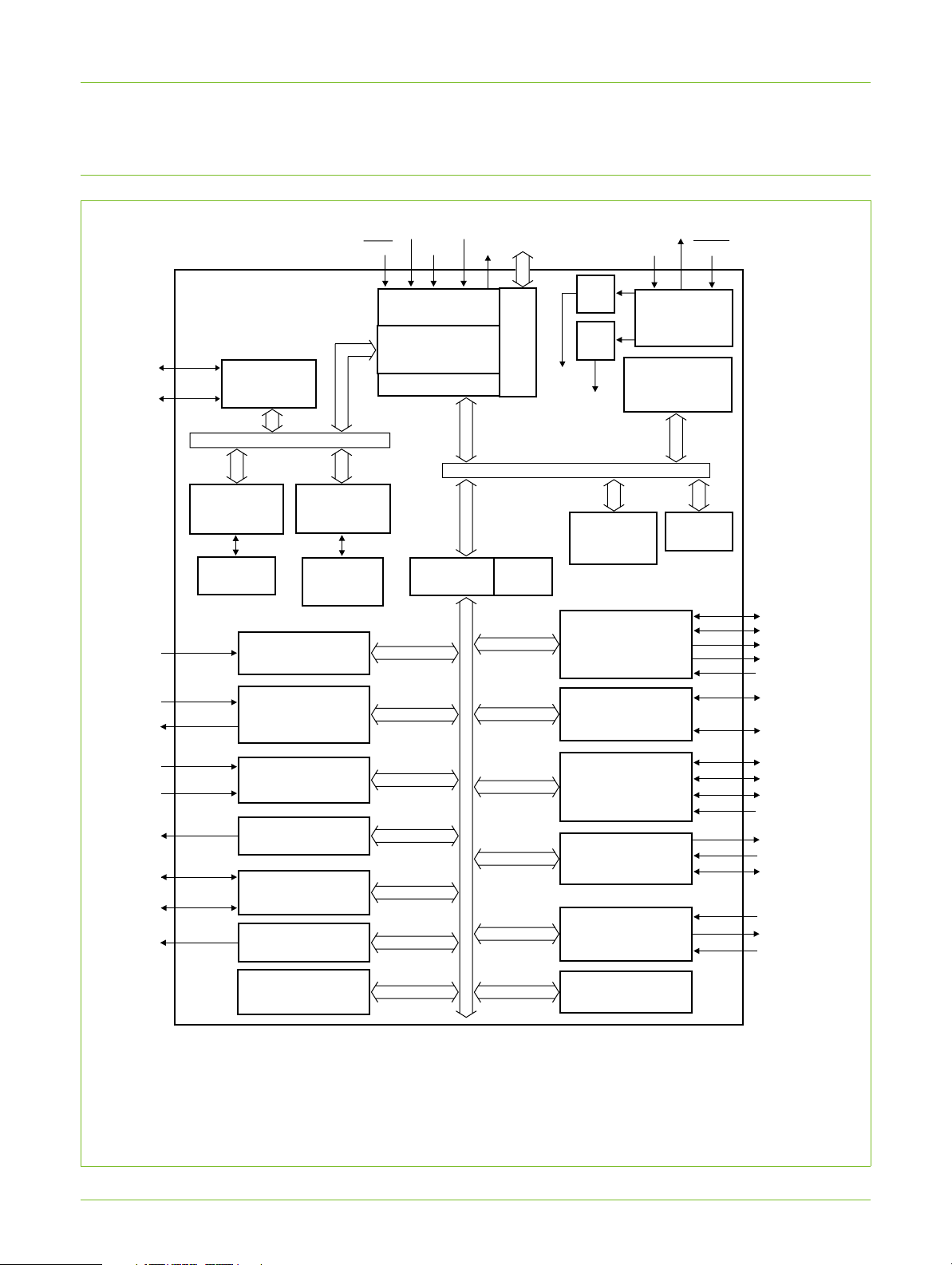
9. Block diagram
UM10139
Chapter 1: Introductory information
P0[31:28],
P0[25:0]
P1[31:16]
EINT[3:0]
8 × CAP
8 × MAT
LPC2141/42/44/46/48
FAST GENERAL
PURPOSE I/O
ARM7 local bus
INTERNAL
SRAM
CONTROLLER
8/16/32 kB
SRAM
CONTROLLER
EXTERNAL
INTERRUPTS
CAPTURE/
COMPARE
TIMER 0/TIMER 1
INTERNAL
FLASH
32/64/128/
256/512 kB
FLASH
TMS
(1)
TRST
TEST/DEBUG
ARM7TDMI-S
AHB BRIDGE
APB (ARM
peripheral bus)
(1)
TDI
(1)
TCK
INTERFACE
AHB TO APB
BRIDGE
(1)
trace
signals
(1)
TDO
PLL0
PLL1
EMULATION
system
TRACE MODULE
clock
USB
clock
APB
DIVIDER
AMBA AHB
8 kB RAM
SHARED WITH
USB DMA
USB 2.0 FULL-SPEED
DEVICE CONTROLLER
WITH DMA
2
C SERIAL
I
INTERFACES 0 AND 1
(Advanced High-performance Bus)
XTAL2
XTAL1
SYSTEM
FUNCTIONS
VECTORED
INTERRUPT
CONTROLLER
AHB
DECODER
(3)
(3)
RESET
D+
DUP_LED
CONNECT
V
BUS
SCL0,1
SDA0,1
AD0[7:6],
AD0[4:0]
AD1[7:0]
AOUT
P0[31:28],
P0[25:0]
P1[31:16]
PWM[6:1]
A/D CONVERTERS
(2)
(4)
D/A CONVERTER
PURPOSE I/O
0 AND 1
GENERAL
PWM0
SYSTEM
CONTROL
(2)
(4)
SPI AND SSP
SERIAL INTERFACES
UART0/UART1
REAL TIME CLOCK
WATCHDOG
TIMER
002aab560
SCK0,1
MOSI0,1
MISO0,1
SSEL0,1
TXD0,1
RXD0,1
(2)
DSR1
(2)
RTS1
(2)
DCD1
RTCX1
RTCX2
V
BAT
,CTS1
, DTR1
, RI1
(2)
(2)
(2)
(1) Pins shared with GPIO.
(2) LPCC2144/6/8 only.
(3) USB DMA controller with 8 kB of RAM accessible as general purpose RAM and/or DMA is available in LPC2146/8 only.
(4) LPC2142/4/6/8 only.
Fig 1. LPC2141/2/4/6/8 block diagram
UM10139_2 © Koninklijke Philips Electronics N.V. 2006. All rights reserved.
User manual LPC214x Rev. 02 — 25 July 2006 7 of 355
Page 8

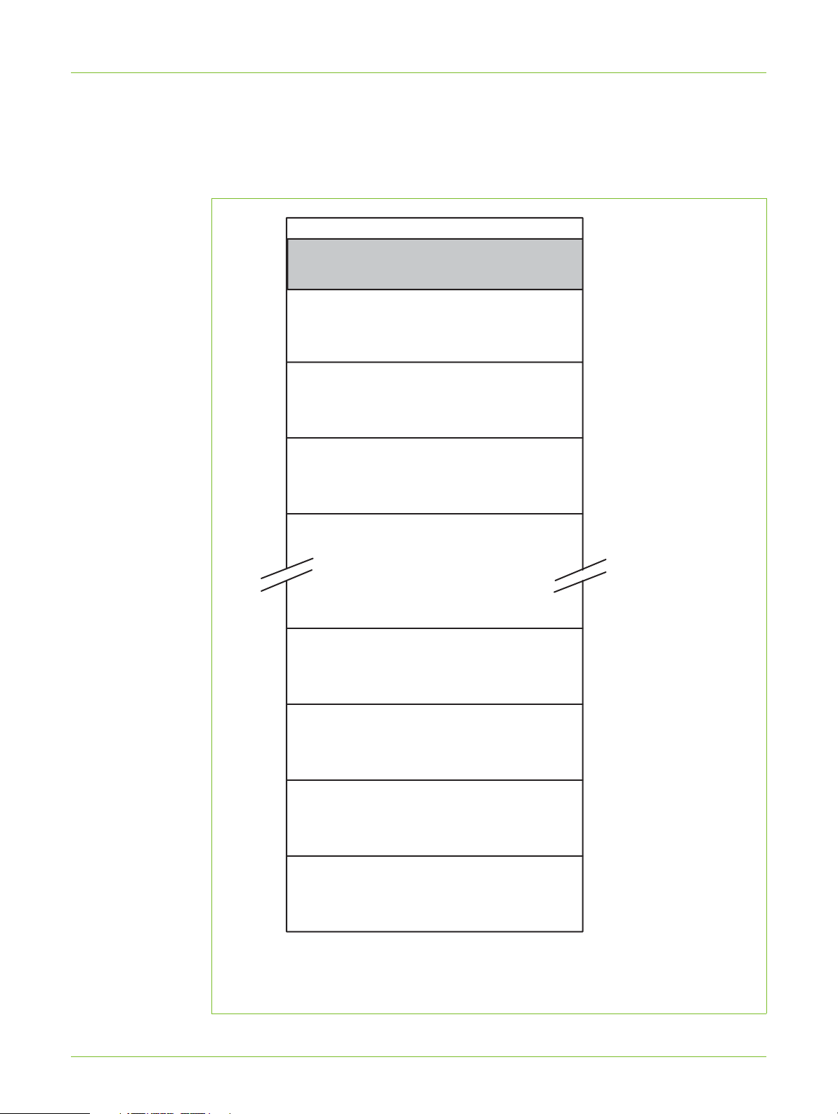
1. Memory maps
The LPC2141/2/4/6/8 incorporates several distinct memory regions, shown in the
following figures. Figure 2–2
user program viewpoint following reset. The interrupt vector area supports address
remapping, which is described later in this section.
3.75 GB
UM10139
Chapter 2: LPC2141/2/4/6/8 Memory addressing
Rev. 02 — 25 July 2006 User manual LPC214x
shows the overall map of the entire address space from the
4.0 GB
AHB PERIPHERALS
APB PERIPHERALS
3.5 GB
0xFFFF FFFF
0xF000 0000
0xE000 0000
3.0 GB
2.0 GB
1.0 GB
0.0 GB
RESERVED ADDRESS SPACE
BOOT BLOCK
(12 kB REMAPPED FROM ON-CHIP FLASH MEMORY)
RESERVED ADDRESS SPACE
8 kB ON-CHIP USB DMA RAM (LPC2146/2148)
RESERVED ADDRESS SPACE
32 kB ON-CHIP STATIC RAM (LPC2146/2148)
16 kB ON-CHIP STATIC RAM (LPC2142/2144)
8 kB ON-CHIP STATIC RAM (LPC2141)
RESERVED ADDRESS SPACE
TOTAL OF 512 kB ON-CHIP NON-VOLATILE MEMORY (LPC2148)
TOTAL OF 256 kB ON-CHIP NON-VOLATILE MEMORY (LPC2146)
TOTAL OF 128 kB ON-CHIP NON-VOLATILE MEMORY (LPC2144)
TOTAL OF 64 kB ON-CHIP NON-VOLATILE MEMORY (LPC2142)
TOTAL OF 32 kB ON-CHIP NON-VOLATILE MEMORY (LPC2141)
0xC000 0000
0x8000 0000
0x7FFF D000
0x7FFF CFFF
0x7FD0 2000
0x7FD0 1FFF
0x7FD0 0000
0x7FCF FFFF
0x4000 8000
0x4000 7FFF
0x4000 4000
0x4000 3FFF
0x4000 2000
0x4000 1FFF
0x4000 0000
0x3FFF FFFF
0x0008 0000
0x0007 FFFF
0x0004 0000
0x0003 FFFF
0x0002 0000
0x0001 FFFF
0x0001 0000
0x0000 FFFF
0x0000 8000
0x0000 7FFF
0x0000 0000
Fig 2. System memory map
UM10139_2 © Koninklijke Philips Electronics N.V. 2006. All rights reserved.
User manual LPC214x Rev. 02 — 25 July 2006 8 of 355
Page 9

Philips Semiconductors
UM10139
Chapter 2: Memory map
4.0 GB
4.0 GB - 2 MB
3.75 GB
0xFFFF FFFF
AHB PERIPHERALS
0xFFE0 0000
0xFFDF FFFF
RESERVED
0xF000 0000
0xEFFF FFFF
RESERVED
3.5 GB + 2 MB
APB PERIPHERALS
3.5 GB
0xE020 0000
0xE01F FFFF
0xE000 0000
Fig 3. Peripheral memory map
Figures 3 through 4 and Table 2–2 show different views of the peripheral address space.
Both the AHB and APB peripheral areas are 2 megabyte sp aces which are divided up into
128 peripherals. Each peripheral space is 16 kilobytes in size. This allows simplifying the
address decoding for each peripheral. All peripheral register addresses are word aligned
(to 32-bit boundaries) regardless of their size. This eliminates the need for byte lane
mapping hardware that would be required to allow byte (8-bit) or half-wor d (16-bit)
UM10139_2 © Koninklijke Philips Electronics N.V. 2006. All rights reserved.
User manual LPC214x Rev. 02 — 25 July 2006 9 of 355
Page 10
Philips Semiconductors
accesses to occur at smaller boundaries. An implication of this is that word and half-word
registers must be accessed all at once. For example, it is not possible to read or write the
upper byte of a word register separately.
UM10139
Chapter 2: Memory map
VECTORED INTERRUPT CONTROLLER
(AHB PERIPHERAL #126)
(AHB PERIPHERAL #125)
(AHB PERIPHERAL #124)
0xFFFF F000 (4G - 4K)
0xFFFF C000
0xFFFF 8000
0xFFFF 4000
0xFFFF 0000
0xFFE1 0000
(AHB PERIPHERAL #3)
0xFFE0 C000
(AHB PERIPHERAL #2)
0xFFE0 8000
(AHB PERIPHERAL #1)
0xFFE0 4000
(AHB PERIPHERAL #0)
0xFFE0 0000
AHB section is 128 x 16 kB blocks (totaling 2 MB).
APB section is 128 x 16 kB blocks (totaling 2MB).
Fig 4. AHB pe riph e ral map
UM10139_2 © Koninklijke Philips Electronics N.V. 2006. All rights reserved.
User manual LPC214x Rev. 02 — 25 July 2006 10 of 355
Page 11

Philips Semiconductors
Table 2. APB peripheries and base addresses
APB peripheral Base address Peripheral name
0 0xE000 0000 Watchdog timer
1 0xE000 4000 Timer 0
2 0xE000 8000 Timer 1
3 0xE000 C000 UART0
4 0xE001 0000 UART1
5 0xE001 4000 PWM
6 0xE001 8000 Not used
7 0xE001 C000 I
8 0xE002 0000 SPI0
9 0xE002 4000 RTC
10 0xE002 8000 GPIO
11 0xE002 C000 Pin connect block
12 0xE003 0000 Not used
13 0xE003 4000 ADC0
14 - 22 0xE003 8000
23 0xE005 C000 I
24 0xE006 0000 ADC1
25 0xE006 4000 Not used
26 0xE006 8000 SSP
27 0xE006 C000 DAC
28 - 35 0xE007 0000
36 0xE009 0000 USB
37 - 126 0xE009 4000
127 0xE01F C000 System Control Block
0xE005 8000
0xE008 C000
0xE01F 8000
2
C0
Not used
2
C1
Not used
Not used
UM10139
Chapter 2: Memory map
2. LPC2141/2142/2144/2146/2148 memory re-mapping and boot block
2.1 Memory map concepts and operating modes
The basic concept on the LPC2141/2/4/6/8 is that each memory area has a "natural"
location in the memory map. This is the address range for which code r esiding in that area
is written. The bulk of each memory space remains permanen tly fixed in the same
location, eliminating the need to have portions of the code designed to run in different
address ranges.
Because of the location of the interrupt vectors on the ARM7 processor (at addresses
0x0000 0000 through 0x0000 001C, as shown in Table 2–3
Boot Block and SRAM spaces need to be re-mapped in order to allow alternative uses of
interrupts in the different operating modes described in Table 2–4
interrupts is accomplished via the Memory Mapping Contro l feature (Section 4–7 “Memor y
mapping control” on page 32).
UM10139_2 © Koninklijke Philips Electronics N.V. 2006. All rights reserved.
User manual LPC214x Rev. 02 — 25 July 2006 11 of 355
below), a small portion of the
. Re-mapping of the
Page 12

Philips Semiconductors
Table 3. ARM exception vector locations
Address Exception
0x0000 0000 Reset
0x0000 0004 Undefined Instruction
0x0000 0008 Software Interrupt
0x0000 000C Prefetch Abort (instruction fetch memory fault)
0x0000 0010 Data Abort (data access memory fault)
0x0000 0014 Reserved
0x0000 0018 IRQ
0x0000 001C FIQ
Table 4. LPC2141/2/4/6/8 memory mapping modes
Mode Activation Usage
Boot
Loader
mode
User
Flash
mode
User RAM
mode
Hardware
activation by
any Reset
Software
activation by
Boot code
Software
activation by
User program
UM10139
Chapter 2: Memory map
Note: Identified as reserved in ARM documentation, this location is used
by the Boot Loader as the Valid User Program key. This is described in
detail in "Flash Memory System and Programming" chapter on page 295.
The Boot Loader always executes after any reset. The Boot Block
interrupt vectors are mapped to the bottom of memory to allow
handling exceptions and using interrupts during the Boot Loading
process.
Activated by Boot Loader when a valid User Program Signature is
recognized in memory and Boot Loader operation is not forced.
Interrupt vectors are not re-mapped and are found in the bottom of the
Flash memory.
Activated by a User Program as desired. Interrupt vectors are
re-mapped to the bottom of the Static RAM.
2.2 Memory re-mapping
In order to allow for compatibility with future derivatives, the entire Boot Block is mapped
to the top of the on-chip memory space. In this manner, the use of larger or smaller flash
modules will not require changing the location of the Boot Block (which would require
changing the Boot Loader code itself) or changing the mapping of the Boot Block interru pt
vectors. Memory spaces other than the interrupt vectors remain in fixed locations.
Figure 2–5
The portion of memory that is re-mapped to allow interrupt processing in different modes
includes the interrupt vector area (32 bytes) and an additional 32 bytes, for a total of
64 bytes. The re-mapped code locations overlay addresses 0x0000 0000 through
0x0000 003F. A typical user program in the Flash memory can place the entire FIQ
handler at address 0x0000 001C without any need to consider memory boundaries. The
vector contained in the SRAM, external memory, and Boot Block must contain branches to
the actual interrupt handlers, or to other instructions that accomplish the branch to the
interrupt handlers.
There are three reasons this configuration was chosen:
1. To give the FIQ handler in the Flash memory the advantage of not having to take a
UM10139_2 © Koninklijke Philips Electronics N.V. 2006. All rights reserved.
User manual LPC214x Rev. 02 — 25 July 2006 12 of 355
shows the on-chip memory mapping in the modes defined above.
memory boundary caused by the remapping into account.
Page 13

Philips Semiconductors
2. Minimize the need to for the SRAM and Boot Block vectors to deal with arbitrary
boundaries in the middle of code space.
3. To provide space to store constants for jumping beyond the range of single word
branch instructions.
Re-mapped memory areas, including the Boot Block and interrupt vectors, continue to
appear in their original location in addition to the re-mapped address.
Details on re-mapping and examples can be found in Section 4–7 “Memory mapping
control” on page 32.
UM10139
Chapter 2: Memory map
UM10139_2 © Koninklijke Philips Electronics N.V. 2006. All rights reserved.
User manual LPC214x Rev. 02 — 25 July 2006 13 of 355
Page 14

Philips Semiconductors
2.0 GB
2.0 GB - 12 kB
12 kB BOOT BLOCK
(RE-MAPPED FROM TOP OF FLASH MEMORY)
(BOOT BLOCK INTERRUPT VECTORS)
RESERVED ADDRESSING SPACE
UM10139
Chapter 2: Memory map
0x8000 0000
0x7FFF FFFF
0x7FFF D000
0x7FFF CFFF
1.0 GB
32 kB ON-CHIP SRAM
(SRAM INTERRUPT VECTORS)
RESERVED ADDRESSING SPACE
(12 kB BOOT BLOCK RE-MAPPED TO HIGHER ADDRESS RANGE)
512 kB FLASH MEMORY
0x4000 8000
0x4000 7FFF
0x4000 0000
0x3FFF FFFF
0x0008 0000
0x0007 FFFF
ACTIVE INTERRUPT VECTORS (FROM FLASH, SRAM, OR BOOT
0.0 GB
BLOCK)
0x0000 0000
Remark: Memory regions are not drawn to scale.
Fig 5. Map of lower memory is showing re-mapped and re-mappable areas (LPC2148
with 512 kB Flash)
UM10139_2 © Koninklijke Philips Electronics N.V. 2006. All rights reserved.
User manual LPC214x Rev. 02 — 25 July 2006 14 of 355
Page 15

Philips Semiconductors
3. Prefetch abort and data abort exceptions
The LPC2141/2/4/6/8 generates the appropriate bus cycle ab ort e xception if a n access is
attempted for an address that is in a reserved or unassigned address region. The regions
are:
• Areas of the memory map that are not implemented for a specific ARM derivative. Fo r
the LPC2141/2/4/6/8, this is:
– Address space between On-Chip Non-Volatile Memory and On-Chip SRAM,
labelled "Reserved Address Space" in Figure 2–2
memory address range from 0x0000 8000 to 0x3FFF FFFF, for 64 kB Flash device
this is memory address range from 0x0001 0000 to 0x3FFF FFFF, for 128 kB
Flash device this is memory address range from 0x0002 0000 to 0x3FFF FFFF, for
256 kB Flash device this is memory address range from 0x0004 0000 to
0x3FFF FFFF while for 512 kB Flash device this range is from 0x0008 0000 to
0x3FFF FFFF.
– Address space between On-Chip Static RAM and the Boot Block. Labelled
"Reserved Address Space" in Figure 2–2
address range from 0x4000 2000 to 0x7FFF CFFF, for 16 kB SRAM device this is
memory address range from 0x4000 4000 to 0x7FFF CFFF. For 32 kB SRAM
device this range is from 0x4000 8000 to 0x7FCF FFFF where the 8 kB USB DMA
RAM starts, and from 0x7FD0 2000 to 0x7FFF CFFF.
– Address space between 0x8000 0000 and 0xDFFF FFFF, labelled "Reserved
Adress Space".
– Reserved regions of the AHB and APB spaces. See Figure 2–3
• Unassigned AHB peripheral spaces. See Figure 2–4.
• Unassigned APB peripheral spaces. See Table 2–2.
UM10139
Chapter 2: Memory map
. For 32 kB Flash device this is
. For 8 kB SRAM device this is memory
.
For these areas, both attempted data acce ss and in struction fetch genera te an exception.
In addition, a Prefetch Abort exception is generated for any instruction fetch that maps to
an AHB or APB peripheral address.
Within the address space of an existing APB peripheral, a data abort exception is not
generated in response to an access to an undefined address. Address decoding within
each peripheral is limited to that needed to distinguish defined registers within the
peripheral itself. For example, an access to address 0xE000 D000 (an undefined address
within the UART0 space) may result in an access to the register defined at address
0xE000 C000. Details of such address aliasing within a peripheral space are not defined
in the LPC2141/2/4/6/8 documentation and are not a supported feature.
Note that the ARM core stores the Prefetch Abort flag along with the associated
instruction (which will be meaningless) in the pipeline and processes the abort only if an
attempt is made to execute the instruction fetched from the illegal address. This prevents
accidental aborts that could be caused by prefetches that occur when code is executed
very near a memory boundary.
UM10139_2 © Koninklijke Philips Electronics N.V. 2006. All rights reserved.
User manual LPC214x Rev. 02 — 25 July 2006 15 of 355
Page 16

1. Introduction
2. Operation
UM10139
Chapter 3: Memory Acceleration Module (MAM)
Rev. 02 — 25 July 2006 User manual LPC214x
The MAM block in the LPC2141/2/4/6/8 maximizes the performance of the ARM
processor when it is running code in Flash memory, but does so using a single Flash
bank.
Simply put, the Memory Accelerator Module (MAM) attempts to have the next ARM
instruction that will be needed in its latches in time to prevent CPU fetch stalls. The
LPC2141/2/4/6/8 uses one bank of Flash memory, compared to the two banks used on
predecessor devices. It includes three 128-bit buffers called the Prefetch Buffer, the
Branch Trail Buf fer and the data b uffer. When an Instruction Fetch is not satisfied by either
the Prefetch or Branch Trail Buffer, nor has a prefetch been initiated for that line, the ARM
is stalled while a fetch is initiated for the 128-bit line. If a prefetch has been initiated but not
yet completed, the ARM is stalled for a shorter time. Unless aborted by a da ta access, a
prefetch is initiated as soon as the Flash has completed the previous access. The
prefetched line is latched by the Flash module, but the MAM does not capture the line in
its prefetch buffer until the ARM core present s the address from which the prefetch has
been made. If the core presents a different address from the one from which the prefetch
has been made, the prefetched line is discarded.
The Prefetch and Branch Trail buffers each include four 32-bit ARM instructions or eight
16-bit Thumb instructions. During sequential code execution, typically the Prefetch Buf fe r
contains the current instruction and the entire Flash line that contains it.
The MAM differentiates betwee n in str uction and data accesses. Code and data accesse s
use separate 128-bit buffers. 3 of every 4 sequential 32- bit code or data accesses "hit" in
the buffer without requiring a Flash access (7 of 8 sequ ential 16-bit accesses, 15 of eve ry
16 sequential byte accesses). The fourth (eighth, 16th) sequential data access must
access Flash, aborting any prefetch in progress. When a Flash data access is concluded,
any prefetch that had been in progress is re-initiated.
Timing of Flash read operat ions is programmable and is described later in this section.
In this manner , there is no code fetch penalty for sequential instruction execution when the
CPU clock period is greater than or equal to one fourth of the Flash access time. The
average amount of time spent doing program branches is relatively small (less than 25%)
and may be minimized in ARM (rather than Thumb) code through the use of the
conditional execution feature present in all ARM instructions. This conditional execution
may often be used to avoid small forward branches that would otherwise be necessary.
Branches and other program flow changes cause a break in the sequential flow of
instruction fetches described above. The Branch Trail Buffer captures the line to which
such a non-sequential break occurs. If the same branch is taken again, the next
instruction is taken from the Branch Trail Buffer. When a branch outside the contents of
UM10139_2 © Koninklijke Philips Electronics N.V. 2006. All rights reserved.
User manual LPC214x Rev. 02 — 25 July 2006 16 of 355
Page 17
Philips Semiconductors
the Prefetch and Branch T rail Buffer is taken, a st all of several clocks is needed to load the
Branch Trail buffer. Subsequently, there will typically be no further instructionfetch delays
until a new and different branch occurs.
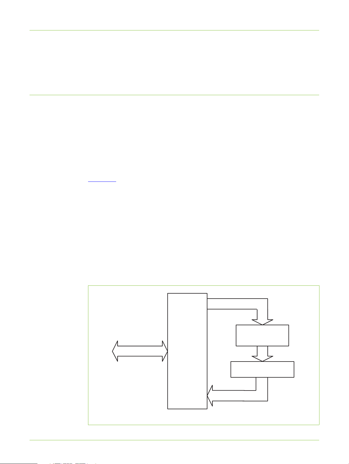
3. MAM blocks
The Memory Accelerator Module is divided into several functional blocks:
• A Flash Address Latch and an incrementor function to form prefetch addresses
• A 128-bit Prefetch Buffer and an associated Address latch and comparator
• A 128-bit Branch Trail Buffer and an associated Address latch and comparator
• A 128-bit Data Buffer and an associated Address latch and comparator
• Control logic
• Wait logic
UM10139
Chapter 3: MAM Module
Figure 3–6
shows a simplified block diagram of the Memory Accelerator Module dat a
paths.
In the following descriptions, the term “fetch” applies to an explicit Flash read request from
the ARM. “Pre-fetch” is used to denote a Flash read of instructions beyond the current
processor fetch address.
3.1 Flash memory bank
There is one bank of Flash memory with the LPC2141/2/4/6/8 MAM.
Flash programming operations are not controlled by the MAM, but are handled as a
separate function. A “boot block” sector contains Flash programming algorithms that may
be called as part of the application program, and a loader that may be run to allow serial
programming of the Flash memory.
MEMORY ADDRESS
FLASH MEMORY BANK
ARM LOCAL BUS
BUS
INTERFACE
BUFFERS
Fig 6. Simplified block diagram of the Memory Accelerator Module (MAM)
UM10139_2 © Koninklijke Philips Electronics N.V. 2006. All rights reserved.
User manual LPC214x Rev. 02 — 25 July 2006 17 of 355
Page 18

Philips Semiconductors
3.2 Instruction latches and data latches
Code and Data accesses are treated separately by the Memory Accelerator Module.
There is a 128-bit Latch, a 15-bit Address
Latch, and a 15-bit comparator associated with each buffer (prefetch, branch trail, and
data). Each 128-bit latch holds 4 words (4 ARM instructions, or 8 Thumb instructions).
Also associated with each buffer are 32 4:1 Multiplexers that select the requested word
from the 128-bit line.
Each Data access that is not in the Data latch causes a Flash fetch of 4 words of data,
which are captured in the Data latch. This speeds up sequential Data operations, but has
little or no effect on random accesses.
3.3 Flash programming issues
Since the Flash memory does not allow accesses during programming and erase
operations, it is necessary for the MAM to force the CPU to wait if a memory access to a
Flash address is requested while the Flash module is busy. (This is accomplished by
asserting the ARM7TDMI-S local bus signal CLKEN.) Under some conditions, this delay
could result in a Watchdog time-out. The user will need to be aware of this possibility and
take steps to insure that an unwanted Watchdog reset does not cause a system failure
while programming or erasing the Flash memory.
UM10139
Chapter 3: MAM Module
In order to preclude the possibility of stale data being read from the Flash memory, the
LPC2141/2/4/6/8 MAM holding latches ar e au to m at i cally inva lida te d at the beg i nning of
any Flash programming or erase operation. Any subsequent read from a Flash address
will cause a new fetch to be initiated after the Flash operation has completed.
4. MAM operating modes
Three modes of operation are defined for the MAM, trading off performance for ease of
predictability:
Mode 0: MAM off. All memory requests result in a Flash read operation (see note 2
below). There are no instruction prefetches.
Mode 1: MAM partially enabled. Sequential instruction accesses are fulfilled from the
holding latches if the data is present. Instruction prefetch is enabled. Non-sequential
instruction accesses initiate Flash read operations (see note 2 below). This means that
all branches cause memory fetches. All data operations cause a Flash read because
buffered data access timing is hard to predict and is very situation dependent.
Mode 2: MAM fully enabled. Any memory request (code or data) for a value that is
contained in one of the corresponding holding latches is fulfilled from the latch.
Instruction prefetch is enabled. Flash read operations are initiated for instruction
prefetch and code or data values not available in the corresponding holding latches.
UM10139_2 © Koninklijke Philips Electronics N.V. 2006. All rights reserved.
User manual LPC214x Rev. 02 — 25 July 2006 18 of 355
Page 19

Philips Semiconductors
T able 5. MAM responses to program accesses of various types
Program Memory Request Type MAM Mode
Sequential access, data in latches Initiate Fetch
Sequential access, data not in latches Initiate Fetch Initiate Fetch
Non-sequential access, data in latches Initiate Fetch
Non-sequential access, data not in latches Initiate Fetch Initiate Fetch
[1] Instruction prefetch is enabled in modes 1 and 2.
[2] The MAM actually uses latched data if it is available, but mimics the timing of a Flash read operation. This
saves power while resulting in the same execution timing. The MAM can truly be turned off by setting the
fetch timing value in MAMTIM to one clock.
T able 6. MAM responses to data and DMA accesses of various types
Data Memory Request T ype MAM Mode
Sequential access, data in latches Initiate Fetch
Sequential access, data not in latches Initiate Fetch Initiate Fetch Initiate Fetch
Non-sequential access, data in latches Initiate Fetch
Non-sequential access, data not in latches Initiate Fetch Initiate Fetch Initiate Fetch
UM10139
Chapter 3: MAM Module
0 1 2
[2]
Use Latched
[1]
Data
[1]
[2]
Initiate Fetch
0 1 2
[1]
Initiate Fetch
[1]
Initiate Fetch
[1][2]
[1]
[1]
[1]
Use Latched
[1]
Data
Initiate Fetch
Use Latched
[1]
Data
Initiate Fetch
Use Latched
Data
Use Latched
Data
[1]
[1]
[1] The MAM actually uses latched data if it is available, but mimics the timing of a Flash read operation. This
saves power while resulting in the same execution timing. The MAM can truly be turned off by setting the
fetch timing value in MAMTIM to one clock.
5. MAM configuration
After reset the MAM defaults to the disabled state. Software can turn memory access
acceleration on or off at any time. This allows most of an application to be run at the
highest possible performance, while certain functions can be run at a somewhat slower
but more predictable rate if more precise timing is required.
6. Register description
All registers, regardless of size, are on word address boundaries. Details of the registers
appear in the description of each function.
UM10139_2 © Koninklijke Philips Electronics N.V. 2006. All rights reserved.
User manual LPC214x Rev. 02 — 25 July 2006 19 of 355
Page 20

Philips Semiconductors
T able 7. Summary of MAM registers
Name Description Access Reset
MAMCR Memory Accelerator Module Control Register.
Determines the MAM functional mode, that is, to
what extent the MAM performance enhancements
are enabled. See Table 3–8
MAMTIM Memory Accelerator Module Timing control.
Determines the number of clocks used for Flash
memory fetches (1 to 7 processor clocks).
[1] Reset value reflects the data stored in used bits only. It does not include reserved bits content.
.
7. MAM Control Register (MAMCR - 0xE01F C000)
Two configuration bits select the three MAM operating modes, as shown in Table 3–8.
Following Reset, MAM functions are disabled. Changing the MAM operating mode causes
the MAM to invalidate all of the holding latches, resulting in new reads of Flash
information as required.
T able 8. MAM Control Register (MAMCR - address 0xE01F C000) bit description
Bit Symbol Value Description Reset
1:0 MAM_mode
_control
7:2 - - Reserved, user software should not write ones to reserved
00 MAM functions disabled 0
01 MAM functions partially enabled
10 MAM functions fully enabled
11 Reserved. Not to be used in the application.
bits. The value read from a reserved bit is not defined.
UM10139
Chapter 3: MAM Module
Address
[1]
value
R/W 0x0 0xE01F C000
R/W 0x07 0xE01F C004
value
NA
8. MAM Timing register (MAMTIM - 0xE01F C004)
The MAM Timing register determines how many CCLK cycles are used to access the
Flash memory. This allows tuning MAM timing to match the processor operating
frequency. Flash access times from 1 clock to 7 clocks ar e po ssib le . Sing le clock Flash
accesses would essentially remove the MAM from timing calculations. In this case the
MAM mode may be selected to optimize power usage.
T able 9. MAM Timing register (MAMTIM - address 0xE01F C004) bit description
Bit Symbol Value Description Reset
value
2:0 MAM_fetch_
cycle_timing
UM10139_2 © Koninklijke Philips Electronics N.V. 2006. All rights reserved.
User manual LPC214x Rev. 02 — 25 July 2006 20 of 355
000 0 - Reserved. 07
001 1 - MAM fetch cycles are 1 processor clock (CCLK) in
duration
010 2 - MAM fetch cycles are 2 CCLKs in duration
011 3 - MAM fetch cycles are 3 CCLKs in duration
100 4 - MAM fetch cycles are 4 CCLKs in duration
101 5 - MAM fetch cycles are 5 CCLKs in duration
Page 21

Philips Semiconductors
T able 9. MAM Timing register (MAMTIM - address 0xE01F C004) bit description
Bit Symbol Value Description Reset
7:3 - - Reserved, user software should not write ones to reserved
9. MAM usage notes
When changing MAM timing, the MAM must first be turned off by writing a zero to
MAMCR. A new value may then be written to MAMTIM. Finally, the MAM may be turned
on again by writing a value (1 or 2) corresponding to the desired operating mode to
MAMCR.
UM10139
Chapter 3: MAM Module
value
110 6 - MAM fetch cycles are 6 CCLKs in duration
111 7 - MAM fetch cycles are 7 CCLKs in duration
Warning: These bits set the duration of MAM Flash fetch operations
as listed here. Improper setting of this value may result in incorrect
operation of the device.
NA
bits. The value read from a reserved bit is not defined.
For system clock slower than 20 MHz, MAMTIM can be 001. For system clock between
20 MHz and 40 MHz, Flash access time is suggested to be 2 CCLKs, while in systems
with system clock faster than 40 MHz, 3 CCLKs are proposed.
UM10139_2 © Koninklijke Philips Electronics N.V. 2006. All rights reserved.
User manual LPC214x Rev. 02 — 25 July 2006 21 of 355
Page 22

UM10139
Chapter 4: System control block
Rev. 02 — 25 July 2006 User manual LPC214x
1. Summary of system control block functions
The System Control Block includes several system features and control registers for a
number of functions that are not related to specific peripheral devices. These include:
• Crystal Oscillator
• External Interrupt Inputs
• Miscellaneous System Controls and Status
• Memory Mapping Control
• PLL
• Power Control
• Reset
• APB Divider
• Wakeup Timer
Each type of function has its own register(s) if any are required and unneeded bits are
defined as reserved in order to allow future expansion. Unrelated functions never share
the same register addresses
2. Pin description
Table 4–10 shows pins that are associated with System Control block functions.
Table 10. Pin summary
Pin name Pin
XTAL1 Input Crystal Oscillator Input - Input to the oscillator and internal clock
XTAL2 Output Crystal Oscillator Output - Output from the oscillator amplifier
EINT0 Input External Interrupt Input 0 - An active low/high level or
EINT1 Input External Interrupt Input 1 - See the EINT0 description above.
Pin description
direction
generator circuits
falling/rising edge general purpose interrupt input. This pin may be
used to wake up the processor from Idle or Power-down modes.
Pins P0.1 and P0.16 can be selected to perform EINT0 function.
Pins P0.3 and P0.14 can be selected to perform EINT1 function.
Remark: LOW level on pin P0.14 immediately after reset is
considered as an external hardware request to start the ISP
command handler. More details on ISP and Serial Boot Loader can
be found in "Flash Memory System and Programming" chapter on
page 295.
UM10139_2 © Koninklijke Philips Electronics N.V. 2006. All rights reserved.
User manual LPC214x Rev. 02 — 25 July 2006 22 of 355
Page 23

Philips Semiconductors
Table 10. Pin summary
Pin name Pin
EINT2 Input External Interrupt Input 2 - See the EINT0 description above.
EINT3 Input External Interrupt Input 3 - See the EINT0 description above.
RESET
3. Register description
All registers, regardless of size, are on word address boundaries. Details of the registers
appear in the description of each function.
T able 11. Summary of system control registers
Name Description Access Reset
External Interrupts
EXTINT External Interrupt Flag Register R/W 0 0xE01F C140
INTWAKE Interrupt Wakeup Register R/W 0 0xE01F C144
EXTMODE External Interrupt Mode Register R/W 0 0xE01F C148
EXTPOLAR External Interrupt Polarity Register R/W 0 0xE01F C14C
Memory Mapping Control
MEMMAP Memory Mapping Control R/W 0 0xE01F C040
Phase Locked Loop
PLL0CON PLL0 Control Register R/W 0 0xE01F C080
PLL0CFG PLL0 Configuration Register R/W 0 0xE01F C084
PLL0STAT PLL0 Status Register RO 0 0xE01F C088
PLL0FEED PLL0 Feed Register WO NA 0xE01F C08C
PLL1CON PLL1 (USB) Control Register R/W 0 0xE01F C0A0
PLL1CFG PLL1 (USB) Configuration Register R/W 0 0xE01F C0A4
PLL1STAT PLL1 (USB) Status Register RO 0 0xE01F C0A8
PLL1FEED PLL1 (USB) Feed Register WO NA 0xE01F C0AC
Power Control
PCON Power Control Register R/W 0 0xE01F C0C0
PCONP Power Control for Peripherals R/W 0x03BE 0xE01F C0C4
APB Divider
APBDIV APB Divider Control R/W 0 0xE01F C100
Reset
RSID Reset Source Identification Register R/W 0 0xE01F C180
Code Security/Debugging
UM10139
Chapter 4: System control block
Pin description
direction
Pins P0.7 and P0.15 can be selected to perform EINT2 function.
Pins P0.9, P0.20 and P0.30 can be selected to perform EINT3
function.
Input External Reset input - A LOW on this pin resets the chip, causing
I/O ports and peripherals to take on their default states, and the
processor to begin execution at address 0x0000 0000.
Address
value
[1]
UM10139_2 © Koninklijke Philips Electronics N.V. 2006. All rights reserved.
User manual LPC214x Rev. 02 — 25 July 2006 23 of 355
Page 24

Philips Semiconductors
T able 11. Summary of system control registers
Name Description Access Reset
CSPR Code Security Protection Register RO 0 0xE01F C184
Syscon Miscellaneous Registers
SCS System Controls and Status R/W 0 0xE01F C1A0
[1] Reset value reflects the data stored in used bits only. It does not include reserved bits content.
4. Crystal oscillator
While an input signal of 50-50 duty cycle within a frequency range from 1 MHz to 50 MHz
can be used by the LPC2141/2/4/6/8 if supplied to its input XTAL1 pin, this
microcontroller’s onboard oscillator circuit supports external crystals in the range of 1 MHz
to 30 MHz only . If the on-chip PLL system or the boot-loader is used, the input clock
frequency is limited to an exclusive range of 10 MHz to 25 MHz.
UM10139
Chapter 4: System control block
Address
value
[1]
The oscillator output frequency is called F
referred to as CCLK for purposes of rate equations, etc. elsewhere in this document. F
and the ARM processor clock frequency is
OSC
OSC
and CCLK are the same value unless the PLL is running and connected. Refer to the
Section 4–8 “Phase Locked Loop (PLL)” on page 33
for details and frequency limitations.
The onboard oscillator in the LPC2141/2/4/6/8 can operate in one of two modes: slave
mode and oscillation mode.
In slave mode the input clock signal should be coupled by means of a capacitor of 100 pF
(C
in Figure 4–7, drawing a), with an amplitude of at least 200 mV rms. The X2 pin in this
C
configuration can be left not connected. If slave mode is selected, the F
signal of
OSC
50-50 duty cycle can range from 1 MHz to 50 MHz.
External components and models used in oscillation mode are shown in Figure 4–7
drawings b and c, and in Table 4–12
only a crystal and the capacitances C
. Since the feedback resistance is integrated on chip,
and CX2 need to be connected externally in case
X1
of fundamental mode oscillation (the fundamental frequency is represented by L, C
R
). Capacitance CP in Figure 4–7, drawing c, represents the parallel package
S
capacitance and should not be larger than 7 pF. Parameters F
, CL, RS and CP are
C
,
and
L
supplied by the crystal manufacturer.
Choosing an oscillation mode as an on-board oscillator mode of operation limits F
OSC
clock selection to 1 MHz to 30 MHz.
UM10139_2 © Koninklijke Philips Electronics N.V. 2006. All rights reserved.
User manual LPC214x Rev. 02 — 25 July 2006 24 of 355
Page 25
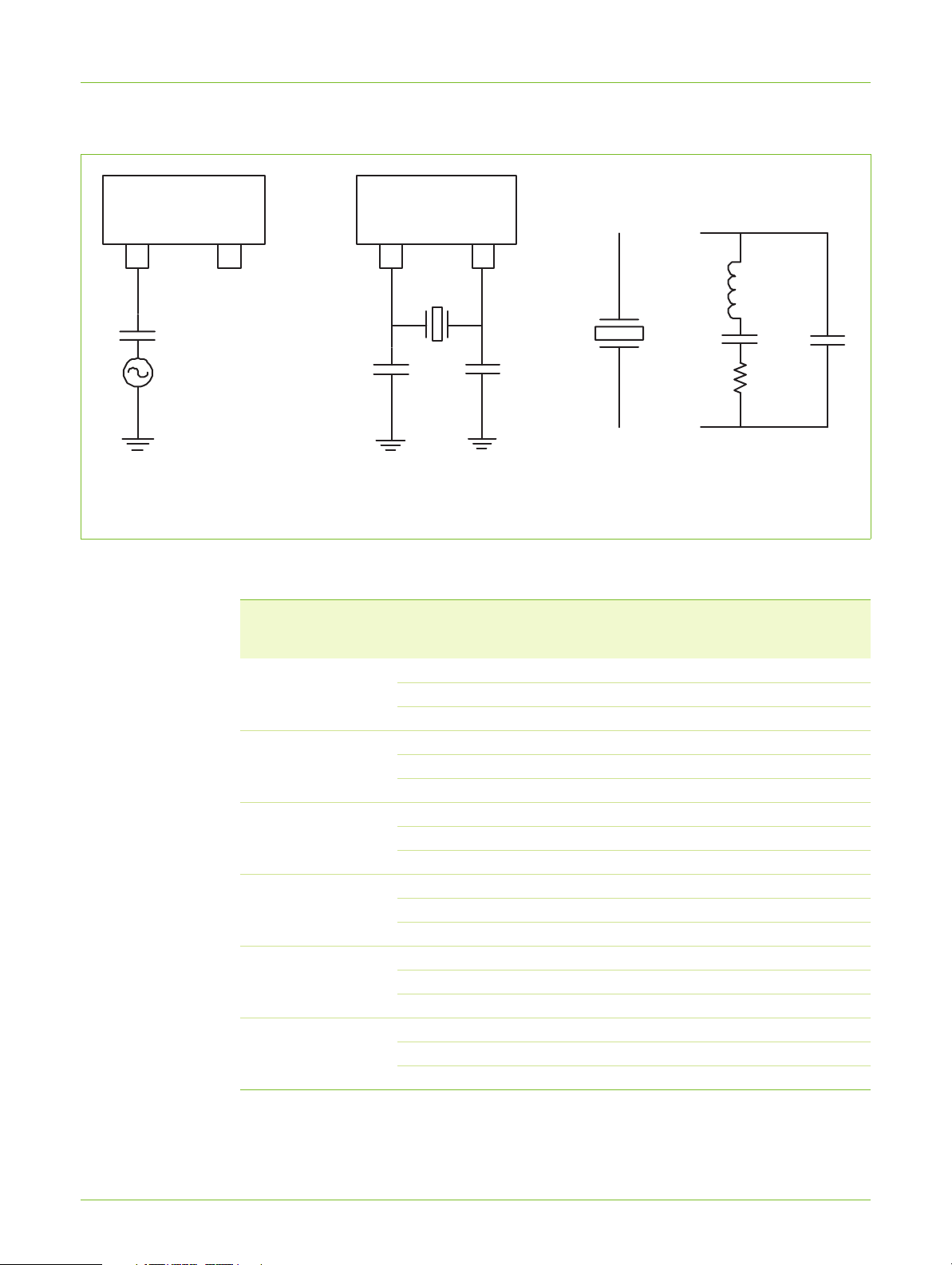
Philips Semiconductors
LPC214x LPC214x
UM10139
Chapter 4: System control block
XTAL1 XTAL2
C
C
Clock
a) b) c)
XTAL1 XTAL2
C
X1
Xtal
L
< = >
C
X2
C
L
R
S
Fig 7. Oscillator modes and models: a) slave mode of operation, b) oscillation mode of operation, c) external
crystal model used for CX1/X2 evaluation
T able 12. Recommended values for C
in oscillation mode (crystal and external
X1/X2
components parameters)
Fundamental
oscillation frequency
F
OSC
Crystal load
capacitance C
Maximum crystal
L
series resistance R
External load
capacitors CX1,
S
1 MHz - 5 MHz 10 pF NA NA
20 pF NA NA
30 pF < 300 Ω 58 pF, 58 pF
5 MHz - 10 MHz 10 pF < 300Ω 18 pF, 18 pF
20 pF < 300 Ω 38 pF, 38 pF
30 pF < 300 Ω 58 pF, 58 pF
10 MHz - 15 MHz 10 pF < 300 Ω 18 pF, 18 pF
20 pF < 220 Ω 38 pF, 38 pF
30 pF < 140 Ω 58 pF, 58 pF
15 MHz - 20 MHz 10 pF < 220 Ω 18 pF, 18 pF
20 pF < 140 Ω 38 pF, 38 pF
30 pF < 80 Ω 58 pF, 58 pF
20 MHz - 25 MHz 10 pF < 160 Ω 18 pF, 18 pF
20 pF < 90 Ω 38 pF, 38 pF
30 pF < 50 Ω 58 pF, 58 pF
25 MHz - 30 MHz 10 pF < 130 Ω 18 pF, 18 pF
20 pF < 50 Ω 38 pF, 38 pF
30 pF NA NA
CX2
C
P
UM10139_2 © Koninklijke Philips Electronics N.V. 2006. All rights reserved.
User manual LPC214x Rev. 02 — 25 July 2006 25 of 355
Page 26
Philips Semiconductors
f
OSC
UM10139
Chapter 4: System control block
selection
MIN f
= 10 MHz
OSC
MAX f
= 25 MHz
OSC
mode a and/or b mode a mode b
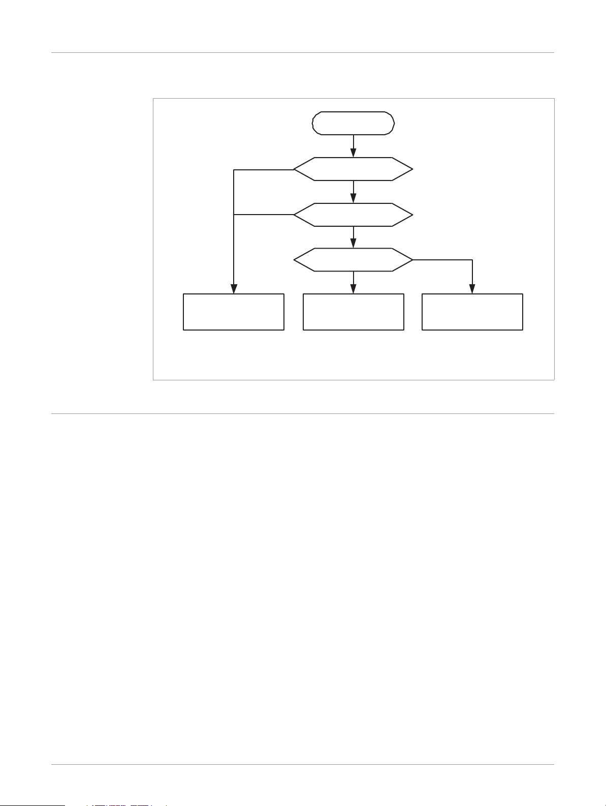
Fig 8. F
selection algorithm
OSC
5. External interrupt inputs
The LPC2141/2/4/6/8 includes four External Interrupt Inputs as selectable pin functions.
The External Interrupt Inputs can optionally be used to wake up the processor from
Power-down mode.
true
true
on-chip PLL used
in application?
false
ISP used for initial
code download?
false
external crystal
oscillator used?
false
MIN f
= 1 MHz
OSC
MAX f
= 50 MHz
OSC
true
MIN f
MAX f
= 1 MHz
OSC
= 30 MHz
OSC
5.1 Register description
The external interrupt function has four registers associated with it. The EXTINT register
contains the interrupt flags, and the EXTWAKEUP register contains bits that enable
individual external interrupts to wake up the microcontroller from Power-down mode. The
EXTMODE and EXTPOLAR registers specify the level and edge sensitivity parameters.
UM10139_2 © Koninklijke Philips Electronics N.V. 2006. All rights reserved.
User manual LPC214x Rev. 02 — 25 July 2006 26 of 355
Page 27

Philips Semiconductors
Table 13. External interrupt registers
Name Description Access Reset
EXTINT The External Interrupt Flag Register contains
INTWAKE The Interrupt Wakeup Register contains four
EXTMODE The External Interrupt Mode Register controls
EXTPOLAR The External Interrupt Polarity Register controls
[1] Reset value reflects the data stored in used bits only. It does not include reserved bits content.
5.2 External Interrupt Flag register (EXTINT - 0xE01F C140)
interrupt flags for EINT0, EINT1, EINT2 and
EINT3. See Table 4–14
enable bits that control whether each external
interrupt will cause the processor to wake up
from Power-down mode. See Table 4–15
whether each pin is edge- or level sensitive.
which level or edge on each pin will cause an
interrupt.
.
.
UM10139
Chapter 4: System control block
Address
[1]
value
R/W 0 0xE01F C140
R/W 0 0xE01F C144
R/W 0 0xE01F C148
R/W 0 0xE01F C14C
When a pin is selected for its external interrupt function, the level or edge on that pin
(selected by its bits in the EXTPOLAR a nd EXTMODE registers) will set its interrupt fla g in
this register. This asserts the corresponding interrupt request to the VIC, which will cause
an interrupt if interrupts from the pin are enabled.
Writing ones to bits EINT0 through EINT3 in EXTINT register clears the corre sp onding
bits. In level-sensitive mode this action is efficacious only when the pin is in its inactive
state.
Once a bit from EINT0 to EINT3 is set and an appropriate code star ts to execute (hand ling
wakeup and/or external interrupt), this bit in EXTINT register must be cleared. Otherwise
the event that was just triggered by activity on the EINT pin will not be recognized in the
future.
Remark: whenever a change of external interrupt operating mode (i.e. active level/edge)
is performed (including the initialization of an external interrupt), the corresponding bit in
the EXTINT register must be cleared! For details see Section 4–5.4 “External Interrupt
Mode register (EXTMODE - 0xE01F C148)” and Section 4–5.5 “Exter nal Interrupt Polarity
register (EXTPOLAR - 0xE01F C14C)”.
For example, if a system wakes up from power-down using a low level on external
interrupt 0 pin, its post-wakeup code must reset the EINT0 bit in order to a llow future entry
into the power-down mode. If the EINT0 bit is left set to 1, subsequent attempt(s) to invoke
power-down mode will fail. The same goes for external interrupt handling.
More details on power-down mode will be discussed in the following chapters.
UM10139_2 © Koninklijke Philips Electronics N.V. 2006. All rights reserved.
User manual LPC214x Rev. 02 — 25 July 2006 27 of 355
Page 28

Philips Semiconductors
UM10139
Chapter 4: System control block
Table 14. External Interrupt Flag register (EXTINT - address 0xE01F C140) bit description
Bit Symbol Description Reset
0 EINT0 In level-sensitive mode, this bit is set if the EINT0 function is selected for its pin, and the pin is in
1 EINT1 In level-sensitive mode, this bit is set if the EINT1 function is selected for its pin, and the pin is in
2 EINT2 In level-sensitive mode, this bit is set if the EINT2 function is selected for its pin, and the pin is in
3 EINT3 In level-sensitive mode, this bit is set if the EINT3 function is selected for its pin, and the pin is in
7:4 - Reserved, user software should not write ones to reserved bits. The value read from a reserved
value
0
its active state. In edge-sensitive mode, this bit is set if the EINT0 function is selected for its pin,
and the selected edge occurs on the pin.
Up to two pins can be selected to perform the EINT0 function (see P0.1 and P0.16 description in
"Pin Configuration" chapter page 66.)
This bit is cleared by writing a one to it, except in level sensitive mode when the pin is in its
active state (e.g. if EINT0 is selected to be low level sensitive and a low level is present on the
corresponding pin, this bit can not be cleared; this bit can be cleared only when the signal on the
pin becomes high).
0
its active state. In edge-sensitive mode, this bit is set if the EINT1 function is selected for its pin,
and the selected edge occurs on the pin.
Up to two pins can be selected to perform the EINT1 function (see P0.3 and P0.14 description in
"Pin Configuration" chapter on page 66.)
This bit is cleared by writing a one to it, except in level sensitive mode when the pin is in its
active state (e.g. if EINT1 is selected to be low level sensitive and a low level is present on the
corresponding pin, this bit can not be cleared; this bit can be cleared only when the signal on the
pin becomes high).
0
its active state. In edge-sensitive mode, this bit is set if the EINT2 function is selected for its pin,
and the selected edge occurs on the pin.
Up to two pins can be selected to perform the EINT2 function (see P0.7 and P0.15 description in
"Pin Configuration" chapter on page 66.)
This bit is cleared by writing a one to it, except in level sensitive mode when the pin is in its
active state (e.g. if EINT2 is selected to be low level sensitive and a low level is present on the
corresponding pin, this bit can not be cleared; this bit can be cleared only when the signal on the
pin becomes high).
0
its active state. In edge-sensitive mode, this bit is set if the EINT3 function is selected for its pin,
and the selected edge occurs on the pin.
Up to three pins can be selected to perform the EINT3 function (see P0.9, P0.20 and P0.30
description in "Pin Configuration" chapter on page 66.)
This bit is cleared by writing a one to it, except in level sensitive mode when the pin is in its
active state (e.g. if EINT3 is selected to be low level sensitive and a low level is present on the
corresponding pin, this bit can not be cleared; this bit can be cleared only when the signal on the
pin becomes high).
NA
bit is not defined.
5.3 Interrupt Wakeup register (INTWAKE - 0xE01F C144)
Enable bits in the INTWAKE register allow the external interrupts and other sources to
wake up the processor if it is in Power-down mode. The related EINTn function must be
mapped to the pin in order for the wakeup process to take place. It is not nece ssary for the
interrupt to be enabled in the Vectored Interrupt Controller for a wakeup to take place.
This arrangement allows additional capabilities, such as having an external interrupt input
wake up the processor from Power-down mode without causing an interrupt (simply
resuming operation), or allowing an interrupt to be enabled during Power-down without
waking the processor up if it is asserted (eliminating the need to disable the interrupt if the
wakeup feature is not desirable in the application).
UM10139_2 © Koninklijke Philips Electronics N.V. 2006. All rights reserved.
User manual LPC214x Rev. 02 — 25 July 2006 28 of 355
Page 29

Philips Semiconductors
For an external interrupt pin to be a source that would wake up the microco ntroller from
Power-down mode, it is also necessary to clear the corresponding bit in the External
Interrupt Flag register (Section 4–5.2 on page 27
Table 15. Interrupt Wakeup register (INTWAKE - address 0xE01F C144) bit description
Bit Symbol Description Reset
0 EXTWAKE0 When one, assertion of EINT0 will wake up the processor from
1 EXTWAKE1 When one, assertion of EINT1 will wake up the processor from
2 EXTWAKE2 When one, assertion of EINT2 will wake up the processor from
3 EXTWAKE3 When one, assertion of EINT3 will wake up the processor from
4 - Reserved, user software should not write ones to reserved bits.
5 USBWAKE When one, activity of the USB bus (USB_need_clock = 1) will
13:4 - Reserved, user software should not write ones to reserved bits.
14 BODWAKE When one, a BOD interrupt will wake up the processor from
15 RTCWAKE When one, assertion of an RTC interrupt will wake up the
UM10139
Chapter 4: System control block
).
value
0
Power-down mode.
0
Power-down mode.
0
Power-down mode.
0
Power-down mode.
NA
The value read from a reserved bit is not defined.
0
wake up the processor from Power-down mode. Any change of
state on the USB data pins will cause a wakeup when this bit is
set. For details on the relationship of USB to Power-down mode
and wakeup, see Section 14–7.1 “USB Interrupt Status register
(USBIntSt - 0xE01F C1C0)” on page 200 and Section 4–8.8
“PLL and Power-down mode” on page 38.
NA
The value read from a reserved bit is not defined.
0
Power-down mode.
0
processor from Power-down mode.
5.4 E xternal Interrupt Mode register (EXTMODE - 0xE01F C148)
The bits in this register select whether each EI NT pin is le vel- or edge- sensitive. Only pins
that are selected for the EINT function (see chapter Pin Connect Block on page 74) and
enabled via the VICIntEnable register (Section 5–4.4 “Interrupt Enable register
(VICIntEnable - 0xFFFF F010)” on page 54) can cause interrupts from the External
Interrupt function (though of course pins selected for other functions may cause i nterrupt s
from those functions).
Note: Software should only change a bit in this register when its interrupt is
disabled in the VICIntEnable register, and should write the corresponding 1 to the
EXTINT register before enabling (initializing) or re-enabling the interrupt, to clear
the EXTINT bit that could be set by changing the mode.
Table 16. External Interrupt Mode register (EXTMODE - address 0xE01F C148) bit
description
Bit Symbol Value Description Reset
value
0 EXTMODE0 0 Level-sensitivity is selected for EINT0. 0
1 EINT0 is edge sensitive.
1 EXTMODE1 0 Level-sensitivity is selected for EINT1. 0
UM10139_2 © Koninklijke Philips Electronics N.V. 2006. All rights reserved.
User manual LPC214x Rev. 02 — 25 July 2006 29 of 355
Page 30

Philips Semiconductors
Table 16. External Interrupt Mode register (EXTMODE - address 0xE01F C148) bit
Bit Symbol Value Description Reset
2 EXTMODE2 0 Level-sensitivity is selected for EINT2. 0
3 EXTMODE3 0 Level-sensitivity is selected for EINT3. 0
7:4 - - Reserved, user software should not write ones to reserved
5.5 External Interrupt Polarity register (EXTPOLAR - 0xE01F C14C)
In level-sensitive mode, the bits in this register select whether the corresponding pin is
high- or low-active. In edge-sensitive mode, they select whether the pin is rising- or
falling-edge sensitive. Only pins that are selected for the EINT function (see "Pin Connect
Block" chapter on page 74) and enabled in the VICIntEnable register (Section 5–4.4
“Interrupt Enable register (VICIntEnable - 0xFFFF F010)” on page 54) can cause
interrupts from the External Interrupt function (though of course pins selected for other
functions may cause interrupts from those functions).
UM10139
Chapter 4: System control block
description
value
1 EINT1 is edge sensitive.
1 EINT2 is edge sensitive.
1 EINT3 is edge sensitive.
NA
bits. The value read from a reserved bit is not defined.
Remark: Software should only change a bit in this register when it s interrupt is disabled in
the VICIntEnable register, and should write the corresponding 1 to the EXTINT register
before enabling (initializing) or re-enabling the interrupt, to cle ar the EXTINT bit th at could
be set by changing the polarity.
Table 17. External Interrupt Polarity register (EXTPOLAR - address 0xE01F C14C) bit
description
Bit Symbol Value Description Reset
value
0 EXTPOLAR0 0 EINT0 is low-active or falling-edge sensitive (see EXTMODE0) 0
1 EINT0 is high-active or rising-edge sensitive (see EXTMODE0)
1 EXTPOLAR1 0 EINT1 is low-active or falling-edge sensitive (see EXTMODE1) 0
1 EINT1 is high-active or rising-edge sensitive (see EXTMODE1)
2 EXTPOLAR2 0 EINT2 is low-active or falling-edge sensitive (see EXTMODE2) 0
1 EINT2 is high-active or rising-edge sensitive (see EXTMODE2)
3 EXTPOLAR3 0 EINT3 is low-active or falling-edge sensitive (see EXTMODE3) 0
1 EINT3 is high-active or rising-edge sensitive (see EXTMODE3)
7:4 - - Reserved, user software should not write ones to reserved bits.
The value read from a reserved bit is not defined.
NA
5.6 Multiple external interrupt pins
Software can select multiple pins for each of EINT3:0 in the Pin Select registers, which
are described in chapter Pin Connect Block on page 74. The external interrupt logic for
each of EINT3:0 receives the state of all of its associated pins from the pins’ receivers,
along with signals that indicate whether each pin is selected for the EINT function. The
external interrupt logic handles the case when m ore than one pin is so selected, dif ferently
according to the state of its Mode and Polarity bits:
UM10139_2 © Koninklijke Philips Electronics N.V. 2006. All rights reserved.
User manual LPC214x Rev. 02 — 25 July 2006 30 of 355
Page 31

Philips Semiconductors
• In Low-Active Level Sensitive mode, the states of all pins selected for the same EINTx
functionality are digitally combined using a positive logic AND gate.
• In High-Active Level Sensitive mode, the states of all pins selected for the same
EINTx functionality are digitally combined using a positive logic OR gate.
• In Edge Sensitive mode, regardless of polarity, the pin with the lowest GPIO port
number is used. (Selecting multiple pins for an EINTx in edge-sensitive mode could
be considered a programming error.)
The signal derived by this logic processing multiple external interrupt pins is the EINTi
signal in the following logic schematic Figure 4–9
For example, if the EINT3 function is selected in the PINSEL0 and PINSEL1 registers for
pins P0.9, P0.20 and P0.30, and EINT3 is configured to be low level sensitive, the inputs
from all three pins will be logically ANDed. When more than one EINT pin is logically
ORed, the interrupt service routine can read the states of the pins from the GPIO port
using the IO0PIN and IO1PIN registers, to determine which pin(s) caused the interrupt.
UM10139
Chapter 4: System control block
.
EINTi
EXTPOLARi
EXTMODEi
APB Bus Data
GLITCH
FILTER
reset
write 1 to EXTINTi
wakeup enable
(one bit of EXTWAKE)
D Q
PCLK
1
D
APB Read
of EXTWAKE
EINTi to wakeup
1
timer
interrupt flag
(one bit of EXTINT)
S
Q
S
R
PCLK
S
Q
Q
R
PCLK
to VIC
APB read of
EXTINT
Fig 9. External interrupt logic
6. Other system controls
Some aspects of controlling LPC2141/2/4/6/8 operation that do not fit into peripheral or
other registers are grouped here.
UM10139_2 © Koninklijke Philips Electronics N.V. 2006. All rights reserved.
User manual LPC214x Rev. 02 — 25 July 2006 31 of 355
Page 32

Philips Semiconductors
UM10139
Chapter 4: System control block
6.1 System Control and Status flags register (SCS - 0xE01F C1A0)
Table 18. System Control and Status flags register (SCS - address 0xE01F C1A0) bit description
Bit Symbol Value Description Reset
0 GPIO0M GPIO port 0 mode selection. 0
1 GPIO1M GPIO port 1 mode selection. 0
31:2 - Reserved, user software should not write ones to reserved bits. The value read from
value
0 GPIO port 0 is accessed via APB addresses in a fashion compatible with previous
LCP2000 devices.
1 High speed GPIO is enabled on GPIO port 0, accessed via addresses in the on-chip
memory range. This mode includes the port masking feature described in the GPIO
chapter on page page 80.
0 GPIO port 1 is accessed via APB addresses in a fashion compatible with previous
LCP2000 devices.
1 High speed GPIO is enabled on GPIO port 1, accessed via addresses in the on-chip
memory range. This mode includes the port masking feature described in the GPIO
chapter on page page 80.
NA
a reserved bit is not defined.
7. Memory mapping control
The Memory Mapping Control alters the mapping of the interrupt vectors that appear
beginning at address 0x0000 0000. This allows code running in different memory spaces
to have control of the interrupts.
7.1 M emory Mapping control register (MEMMAP - 0xE01F C040)
Whenever an exception handling is necessary , the microcontroller will fetch an instruction
residing on the exception corresponding address as described in Table 2–3 “ARM
exception vector locations” on page 12. The MEMMAP register determines the source of
data that will fill this table.
Table 19. Memory Mapping control register (MEMMAP - address 0xE01F C040) bit
description
Bit Symbol Value Description Reset
1:0 M AP 00 Boot Loader Mode. Interrupt vectors are re-mapped to Boot Block. 00
01 User Flash Mode . Interrupt vectors are not re-mapped and reside
10 User RAM Mode. Interrupt vectors are re-mapped to Static RAM.
11 Reserved. Do not use this option.
Warning: Improper setting of this value may result in incorrect operation of
the device.
7:2 - - Reserved, user software should not write ones to reserved bits.
value
in Flash.
NA
The value read from a reserved bit is not defined.
UM10139_2 © Koninklijke Philips Electronics N.V. 2006. All rights reserved.
User manual LPC214x Rev. 02 — 25 July 2006 32 of 355
Page 33

Philips Semiconductors
7.2 Memory mapping control usage notes
The Memory Mapping Control simply selects one out of three available sources of data
(sets of 64 bytes each) necessary fo r handling ARM exceptions (interrupts).
For example, whenever a Software Interrupt request is generated, the ARM core will
always fetch 32-bit data "residing" on 0x0000 0008 see Table 2–3 “ARM exce ption vector
locations” on page 12. This means that when MEMMAP[1:0]=10 (User RAM Mode), a
read/fetch from 0x0000 0008 will provide data stored in 0x4000 0008. In case of
MEMMAP[1:0]=00 (Boot Loader Mode), a read/fetch from 0x0000 0008 will provide data
available also at 0x7FFF E008 (Boot Block remapped from on-chip Bootloader).
8. Phase Locked Loop (PLL)
There are two PLL modules in the LPC2141/2/4/6/8 microcontroller. The PLL0 is used to
generate the CCLK clock (system clock) while the PLL1 has to supply the clock for the
USB at the fixed rate of 48 MHz. Structurally these two PLLs are identical with exception
of the PLL interrupt capabilities reserved only for the PLL0.
The PLL0 and PLL1 accept an input clock frequency in the range of 10 MHz to 25 MHz
only. The input frequency is multiplied up the range of 10 MHz to 60 MHz for the CCLK
and 48 MHz for the USB clock using a Current Controlled Oscillators (CCO). The
multiplier can be an integer value from 1 to 32 (in practice, the multiplier value cannot be
higher than 6 on the LPC2141/2/4/6/8 due to the upper frequency limit of the CPU). The
CCO operates in the range of 156 MHz to 320 MHz, so there is an additional divider in the
loop to keep the CCO within its frequency range while the PLL is providing the desired
output frequency. The output divider may be set to divide by 2, 4, 8, or 16 to produce the
output clock. Since the minimum output divider value is 2, it is insured that the PLL o utput
has a 50% duty cycle. A block diagram of the PLL is shown in Figure 4–10
UM10139
Chapter 4: System control block
.
PLL activation is controlled via the PLLCON register. The PLL multiplier and divider
values are controlled by the PLLCFG register. These two registers are protected in order
to prevent accidental alteration of PLL parameters or deactivation of the PLL. Since all
chip operations, including the Watchdog Timer, are dependent on the PLL0 when it is
providing the chip clock, accidental changes to the PLL setup could result in unexpected
behavior of the microcontroller. The same concern is present with the PLL1 and the USB.
The protection is accomplished by a feed sequence similar to that of the Watchdog Timer.
Details are provided in the description of the PLLFEED register.
Both PLLs are turned off and bypassed following a chip Reset and when by entering
Power-down mode. The PLL is enabled by software only. The program must configure
and activate the PLL, wait for the PLL to Lock, then connect to the PLL as a clock source.
8.1 Register description
The PLL is controlled by the registers shown in Table 4–20. More detailed descriptions
follow.
Warning: Improper setting of the PLL0 and PLL1 values may result in incorrect
operation of the device and the USB module!
UM10139_2 © Koninklijke Philips Electronics N.V. 2006. All rights reserved.
User manual LPC214x Rev. 02 — 25 July 2006 33 of 355
Page 34

Philips Semiconductors
UM10139
Chapter 4: System control block
Table 20. PLL registers
Generic
Description Access Reset
name
PLLCON PLL Control Register. Holding register for
updating PLL control bits. Values written to this
register do not take effect until a valid PLL feed
sequence has taken place.
PLLCFG PLL Configuration Register. Holding register for
updating PLL configuration values. Values
written to this register do not take effect until a
valid PLL feed sequence has taken place.
PLLSTAT PLL Status Register . Read-back register for PLL
control and configuration information. If
PLLCON or PLLCFG have been written to, but a
PLL feed sequence has not yet occurred, they
will not reflect the current PLL state. Reading
this register provides the actual values
controlling the PLL, as well as the status of the
PLL.
PLLFEED PLL Feed Register. This register enables
loading of the PLL control and configuration
information from the PLLCON and PLLCFG
registers into the shadow registers that actually
affect PLL operation.
System clock
[1]
value
(PLL0)
Address & Name
R/W 0 0xE01F C080
PLL0CON
R/W 0 0xE01F C084
PLL0CFG
RO 0 0xE01F C088
PLL0STAT
WO NA 0xE01F C08C
PLL0FEED
USB 48 MHz
clock (PLL1)
Address & Name
0xE01F C0A0
PLL1CON
0xE01F C0A4
PLL1CFG
0xE01F C0A8
PLL1STAT
0xE01F C0AC
PLL1FEED
[1] Reset value reflects the data stored in used bits only. It does not include reserved bits content.
UM10139_2 © Koninklijke Philips Electronics N.V. 2006. All rights reserved.
User manual LPC214x Rev. 02 — 25 July 2006 34 of 355
Page 35

Philips Semiconductors
PLLC
direct
0
PSEL[1:0]
UM10139
Chapter 4: System control block
CLOCK
SYNCHRONIZATION
PLLE
0
F
OSC
PLOCK
MSEL[4:0]
Fig 10. PLL block diagram
PD
bypass
PHASE-
FREQUENCY
DETECTOR
F
OUT
DIV-BY-M
MSEL<4:0>
CD
PD
CCO
PD
1
CD
F
CCO
0
/2P
0
0
CCLK
1
1
8.2 PLL Control register (PLL0CON - 0xE01F C080, PLL1CON 0xE01F C0A0)
The PLLCON register contains the bits that enable and connect the PLL. Enabling the
PLL allows it to attempt to lock to the current settings of the multiplier and divider values.
Connecting the PLL causes the processor and all chip functions to run from the PLL
output clock. Changes to the PLLCON register do not take effect until a correct PLL feed
sequence has been given (see Section 4–8.7 “PLL Feed register (PLL0FEED -
0xE01F C08C, PLL1FEED - 0xE01F C0AC)” and Section 4–8.3 “PLL Configuration
register (PLL0CFG - 0xE01F C084, PLL1CFG - 0xE01F C0A4)” on page 36).
UM10139_2 © Koninklijke Philips Electronics N.V. 2006. All rights reserved.
User manual LPC214x Rev. 02 — 25 July 2006 35 of 355
Page 36

Philips Semiconductors
Table 21. PLL Control register (PLL0CON - address 0xE01F C080, PLL1CON - address
Bit Symbol Description Reset
0 PLLE PLL Enable. When one, and after a valid PLL feed, this bit will
1 PLLC PLL Connect. When PLLC and PLLE are both set to one, and after a
7:2 - Reserved, user software should not write ones to reserved bits. The
The PLL must be set up, enabled, and Lock established before it may be used as a clock
source. When switching from the oscillator clock to the PLL output or vice versa, internal
circuitry synchronizes the operation in order to ensure that glitches are not generate d.
Hardware does not insure that the PLL is locked before it is connected or automatically
disconnect the PLL if lock is lost during operation. In the event of loss of PLL lock, it is
likely that the oscillator clock has become unstable and disconnecting the PLL will not
remedy the situation.
Chapter 4: System control block
0xE01F C0A0) bit description
activate the PLL and allow it to lock to the requested frequency. See
PLLSTAT register, Table 4–23
valid PLL feed, connects the PLL as the clock source for the
microcontroller. Otherwise, the oscillator clock is used directly by the
microcontroller. See PLLSTAT register, Table 4–23
value read from a reserved bit is not defined.
.
.
UM10139
value
0
0
NA
8.3 PLL Configuration register (PLL0CFG - 0xE01F C084, PLL1CFG 0xE01F C0A4)
The PLLCFG register contains the PLL multiplier and divider values. Changes to the
PLLCFG register do not take ef fect until a correct PLL fee d sequence has been give n (see
Section 4–8.7 “PLL Feed register (PLL0FEED - 0xE01F C08C, PLL1FEED 0xE01F C0AC)” on page 38). Calculations for the PLL freque n cy, and multiplier and
divider values are found in the PLL Frequency Calculation section on page 39.
T able 22. PLL Configuration register (PLL0CFG - address 0xE01F C084, PLL1CFG - address
0xE01F C0A4) bit description
Bit Symbol Description Reset
value
4:0 MSEL PLL Multiplier value. Supplies the value "M" in the PLL frequency
calculations.
Note: For details on selecting the right value for MSEL see Section
4–8.9 “PLL frequency calculation” on page 39.
6:5 PSEL PLL Divider value. Supplies the value "P" in the PLL frequency
calculations.
Note: For details on selecting the right value for PSEL see Section
4–8.9 “PLL frequency calculation” on page 39.
7 - Reserved, user software should not write ones to reserved bits. The
value read from a reserved bit is not defined.
0
0
NA
UM10139_2 © Koninklijke Philips Electronics N.V. 2006. All rights reserved.
User manual LPC214x Rev. 02 — 25 July 2006 36 of 355
Page 37

Philips Semiconductors
8.4 PLL Status register (PLL0STAT - 0xE01F C088, PLL1STAT 0xE01F C0A8)
The read-only PLLSTAT register provides the actual PLL parameters that are in effect at
the time it is read, as well as the PLL status. PLLSTAT may disagree with values found in
PLLCON and PLLCFG because changes to those registers do not take effect until a
proper PLL feed has occurred (see Section 4–8.7 “PLL Feed register (PLL0FEED -
0xE01F C08C, PLL1FEED - 0xE01F C0AC)”).
T able 23. PLL Status register (PLL0STAT - address 0xE01F C088, PLL1STAT - address
Bit Symbol Description Reset
4:0 MSEL Read-back for the PLL Multiplier value. This is the value currently
6:5 PSEL Read-back for the PLL Divider value. This is the value currently
7 - Reserved, user software should not write ones to reserved bits. The
8 PLLE Read-back for the PLL Enable bit. When one, the PLL is currently
9 PLLC Read-back for the PLL Connect bit. When PLLC and PLLE are both
10 PLOCK Reflects the PLL Lock status. When zero, the PLL is not locked.
15:11 - Reserved, user software should not write ones to reserved bits. The
UM10139
Chapter 4: System control block
0xE01F C0A8) bit description
value
0
used by the PLL.
0
used by the PLL.
NA
value read from a reserved bit is not defined.
0
activated. When zero, the PLL is turned off. This bit is automatically
cleared when Power-down mode is activated.
0
one, the PLL is connected as the clock source for the
microcontroller. When either PLLC or PLLE is zero, the PLL is
bypassed and the oscillator clock is used directly by the
microcontroller. This bit is automatically cleared when Power-down
mode is activated.
0
When one, the PLL is locked onto the requested frequency.
NA
value read from a reserved bit is not defined.
8.5 PLL Interrupt
The PLOCK bit in the PLLSTAT register is connected to the interrupt controller. This
allows for software to turn on the PLL and continue with other functions witho ut having to
wait for the PLL to achieve lock. When the interrupt occurs (PLOCK = 1), the PLL may be
connected, and the interrupt disabled. For details on how to enable and disabl e the PLL
interrupt, see Section 5–4.4 “Interrupt Enable register (VICIntEnable - 0xFFFF F010)” on
page 54 and Section 5–4.5 “Interrupt Enable Clear register (VICIntEnClear 0xFFFF F014)” on page 55.
PLL interrupt is available only in PLL0, i.e. the PLL that generates the CCLK. USB
dedicated PLL1 does not have this capability.
8.6 PLL Modes
The combinations of PLLE and PLLC are shown in Table 4–24.
UM10139_2 © Koninklijke Philips Electronics N.V. 2006. All rights reserved.
User manual LPC214x Rev. 02 — 25 July 2006 37 of 355
Page 38

Philips Semiconductors
Table 24. PLL Control bit combinations
PLLC PLLE PLL Function
0 0 PLL is turned off and disconnected. The CCLK equals the unmodified clock
0 1 The PLL is active, but not yet connected. The PLL can be connected after
1 0 Same as 00 combination. This prevents the possibility of the PLL being
1 1 The PLL is active and has been connected. CCLK/system clock is sourced
8.7 PLL Feed register (PLL0FEED - 0xE01F C08C, PLL1FEED 0xE01F C0AC)
A correct feed sequence must be written to the PLLFEED register in order for changes to
the PLLCON and PLLCFG registers to take effect. The feed sequence is:
1. Write the value 0xAA to PLLFEED.
2. Write the value 0x55 to PLLFEED.
UM10139
Chapter 4: System control block
input. This combination can not be used in case of the PLL1 since there will be
no 48 MHz clock and the USB can not operate.
PLOCK is asserted.
connected without also being enabled.
from the PLL0 and the USB clock is sourced from the PLL1.
The two writes must be in the correct sequence, and must be consecutive APB bus
cycles. The latter requirement implies that interrupts must be disabled for the duration of
the PLL feed operation. If either of the feed values is incorrect, or one of the previously
mentioned conditions is not met, any changes to the PLLCON or PLLCFG register will not
become effective.
Table 25. PLL Feed register (PLL0FEED - address 0xE01F C08C, PLL1FEED - address
0xE01F C0AC) bit description
Bit Symbol Description Reset
7:0 PLLFEED The PLL fee d sequence must be written to this register in order for
PLL configuration and control register changes to take effect.
8.8 PLL and Power-down mode
Power-down mode automatically turns off and disconnect s activated PLL(s). W akeup from
Power-down mode does not automatically restore the PLL settings, this must be done in
software. Typically, a routine to activate the PLL, wait for lock, and then connect the PLL
can be called at the beginning of any interrupt service routine that might be called due to
the wakeup. It is important not to attempt to restart the PLL by simply feeding it when
execution resumes after a wakeup from Power-down mode. This would enable and
connect the PLL at the same time, before PLL lock is established.
If activity on the USB data lines is not selected to wake up the microcontroller from
Power-down mode (see Section 4–5.3 “Interrupt Wakeup register (INTWAKE -
0xE01F C144)” on page 28), both the system and the USB PLL will be automatically be
turned off and disconnected when Power-down mode is invoked, as described above.
However, in case USBWAKE = 1 and USB_need_clock = 1 it is not possible to go into
Power-down mode and any attempt to set the PD bit will fail, leaving the PLLs in the
current state.
value
0x00
UM10139_2 © Koninklijke Philips Electronics N.V. 2006. All rights reserved.
User manual LPC214x Rev. 02 — 25 July 2006 38 of 355
Page 39

Philips Semiconductors
8.9 PLL frequency calculation
The PLL equations use the following parameters:
T able 26. Elements determining PLL’s frequency
Element Description
F
OSC
F
CCO
CCLK the PLL output frequency (also the processor clock frequency)
M PLL Multiplier value from the MSEL bits in the PLLCFG register
P PLL Divider value from the PSEL bits in the PLLCFG register
The PLL output frequency (when the PLL is both active and connected) is given by:
UM10139
Chapter 4: System control block
the frequency from the crystal oscillator/external oscillator
the frequency of the PLL current controlled oscillator
CCLK = M × F
or CCLK = F
OSC
CCO
/ (2 × P)
The CCO frequency can be computed as:
F
= CCLK × 2 × P or F
CCO
CCO
= F
× M × 2 × P
OSC
The PLL inputs and settings must meet the following:
• F
• CCLK is in the range of 10 MHz to F
is in the range of 10 MHz to 25 MHz.
OSC
(the maximum allowed frequency for the
max
microcontroller - determined by the system microcontroller is embedded in).
• F
is in the range of 156 MHz to 320 MHz.
CCO
8.10 Procedure for determining PLL settings
If a particular application uses the PLL0, its configu ration may be determined as follows:
1. Choose the desired processor operating frequency (CCLK). This may be based on
processor throughput requirements, need to support a specific set of UART baud
rates, etc. Bear in mind that peripheral devices may be running from a lower clock
than the processor (see Section 4–11 “APB divider” on page 46
2. Choose an oscillator frequency (F
multiple of F
OSC
.
3. Calculate the value of M to configure the MSEL bits. M = CCLK / F
the range of 1 to 32. The value written to the MSEL bits in PLLCFG is M − 1 (see
Table 4–28
.
4. Find a value for P to configure the PSEL bits, such that F
frequency limits. F
is calculated using the equation given above. P must have one
CCO
of the values 1, 2, 4, or 8. The value written to the PSEL bits in PLLCFG is 00 for
P = 1; 01 for P = 2; 10 for P = 4; 11 for P = 8 (see Table 4–27
). CCLK must be the whole (non-fractional)
OSC
).
. M must be in
OSC
is within its defined
CCO
).
Remark: if a particular application is using the USB peripheral, the PLL1 must be
configured since this is the only available source of the 48 MHz clock required by the
USB. This limits the selection of FOSC to either 12 MHz, 16 MHz or 24 MHz.
UM10139_2 © Koninklijke Philips Electronics N.V. 2006. All rights reserved.
User manual LPC214x Rev. 02 — 25 July 2006 39 of 355
Page 40

Philips Semiconductors
Table 27. PLL Divider values
PSEL Bits (PLLCFG bit s [6:5]) Value of P
00 1
01 2
10 4
11 8
Table 28. PLL Multiplier values
MSEL Bits (PLLCFG bits [4:0]) Value of M
00000 1
00001 2
00010 3
00011 4
... ...
11110 31
11111 32
UM10139
Chapter 4: System control block
8.11 PLL0 and PLL1 configuring examples
Example 1: an application not using the USB - configuring the PLL0
System design asks for F
Based on these specifications, M = CCLK / Fosc = 60 MHz / 10 MHz = 6. Consequently,
M - 1 = 5 will be written as PLLCFG[4:0].
V alue for P can be d erived from P = F
in range of 156 MHz to 320 MHz. Assuming the lowest allowed frequency for
F
= 156 MHz, P = 156 MHz / (2 x 60 MHz) = 1.3. The highest F
CCO
produces P = 2.67. The only solution for P that satisfies both of these requirements and is
listed in Table 4–27
is P = 2. Therefore, PLLCFG[6:5] = 1 will be used.
Example 2: an application using the USB - configuring the PLL1
System design asks for F
Based on these specifications, M = 48 MHz / Fosc = 48 MHz / 12 MHz = 4. Consequently,
M - 1 = 3 will be written as PLLCFG[4:0].
Value for P can be derived from P = F
be in range of 156 MHz to 320 MHz. Assuming the lowest allowed frequency for
F
= 156 MHz, P = 156 MHz / (2 x 48 MHz) = 1.625. The highest F
CCO
criteria produces P = 3.33. Solution for P that satisfy both of these requirements and are
listed in Table 4–27
are P = 2 and P = 3. Therefore, either of these two values can be
used to program PLLCFG[6:5] in the PLL1.
= 10 MHz and requires CCLK = 60 MHz.
OSC
/ (CCLK x 2), using condition that F
CCO
= 12 MHz and requires the USB clock of 48 MHz.
OSC
/ (48 MHz x 2), using condition that F
CCO
CCO
frequency criteria
CCO
CCO
frequency
CCO
must be
must
Example 2 has illustrated the way PLL1 should be configured. Since PLL0 and PLL1 are
independent, the PLL0 can be configured using the approach described in Example 1.
UM10139_2 © Koninklijke Philips Electronics N.V. 2006. All rights reserved.
User manual LPC214x Rev. 02 — 25 July 2006 40 of 355
Page 41

Philips Semiconductors
9. Power control
The LPC2141/2/4/6/8 supports two reduced power modes: Idle mode and Power-down
mode. In Idle mode, execution of instructions is suspended until eithe r a Reset or interrupt
occurs. Peripheral functions continue operation during Idle mode and may generate
interrupts to cause the processor to resume execution. Idle mode eliminates power used
by the processor itself, memory systems and related controllers, and internal buses.
In Power-down mode, the oscillator is shut down and the chip receives no internal clocks.
The processor state and registers, peripheral registers, and internal SRAM values are
preserved throughout Power-down mode and the logic levels of chip pins remain static.
The Power-down mode can be terminated and normal operation resumed by either a
Reset or certain specific interrupts that are able to function without clocks. Since all
dynamic operation of the chip is suspended, Power-down mode reduces chip power
consumption to nearly zero.
Entry to Power-down and Idle modes must be coordinated with program execution.
Wakeup from Power-down or Idle modes via an interrupt resumes program execution in
such a way that no instructions are lost, incomplete, or repeated. Wake up from
Power-down mode is discussed further in Section 4–12 “Wakeup timer” on page 47
UM10139
Chapter 4: System control block
.
A Power Control for Peripherals feature allows individual peripherals to be turned off if
they are not needed in the application, resulting in additional power savings.
9.1 Register description
The Power Control function contains two registers, as shown in Table 4–29. More detailed
descriptions follow.
Table 29. Power control registers
Name Description Access Reset
PCON Power Control Register. This register contains
control bits that enable the two reduced power
operating modes of the microcontroller. See
Table 4–30
PCONP Power Control for Peripherals Register. This
register contains control bits that enable and
disable individual peripheral functions,
Allowing elimination of power consumption by
peripherals that are not needed.
[1] Reset value reflects the data stored in used bits only. It does not include reserved bits content.
.
R/W 0x00 0xE01F C0C0
R/W 0x0018 17BE 0xE01F C0C4
value
[1]
Address
9.2 Power Control register (PCON - 0xE01F C0C0)
The PCON register contains two bits. Writing a one to the corresponding bit causes entry
to either the Power-down or Idle mode. If both bits are set, Power-down mode is entered.
UM10139_2 © Koninklijke Philips Electronics N.V. 2006. All rights reserved.
User manual LPC214x Rev. 02 — 25 July 2006 41 of 355
Page 42

Philips Semiconductors
Table 30. Power Control register (PCON - address 0xE01F C0C0) bit description
Bit Symbol Value Description Reset
0 IDL Idle mode control. 0
1 PD Power-down mode control. 0
2 BODPDM Brown Out Power-down Mode. 0
3 BOGD Brown Out Global Disable. 0
4 BORD Brown Out Reset Disable. 0
7:5 - Reserved, user software should not write ones to reserved bits.
UM10139
Chapter 4: System control block
0 Idle mode is off.
1 The processor clock is stopped, while on-chip peripherals remain
active. Any enabled interrupt from a peripheral or an external
interrupt source will cause the processor to resume execution.
0 Power-down mode is off.
1 The oscill ator and all on-chip clocks are stopped. A wakeup
condition from an external interrupt can cause the oscillator to
restart, the PD bit to be cleared, and the processor to resume
execution.
Remark: PD bit can be set to 1 at any time if USBWAKE = 0. In
case of USBWAKE = 1, it is possible to set PD to 1 only if
USB_need_clock = 0. Having both USBWAKE and
USB_need_clock equal 1 prevents the microcontroller from
entering Power-down mode. (For additional details see Section
4–5.3 “Interrupt Wakeup register (INTW AKE - 0xE01F C144)” on
page 28 and Section 14–7.1 “USB Interrupt Status register
(USBIntSt - 0xE01F C1C0)” on page 200.
0 Brown Out Dete ction (BOD) remains operative during
Power-down mode, and its Reset can release the microcontroller
from Power-down mode
1 Th e BOD circuitry will go into power down mode when PD = 1,
resulting in a further reduction in power. In this case the BOD can
not be used as a wakeup source from Power Down mode.
0 The BOD circuitry is enabled.
1 The BOD is fully disabled at all times, consuming no power.
0 The reset is enabled. The first stage of low voltage detection
(2.9 V) Brown Out interrupt is not affected.
1 The second stage of low voltage detection (2.6 V) will not cause
a chip reset.
The value read from a reserved bit is not defined.
[1]
.
value
NA
[1] Since execution is delayed until after the Wakeup Timer has allowed the main oscillator to resume stable
operation, there is no guarantee that execution will resume before V
threshold, which prevents execution. If execution does resume, there is no guarantee of how long the
microcontroller will continue execution before the lower BOD threshold terminates execution. These issues
depend on the slope of the decline of V
vicinity of the microcontroller will improve the likelihood that software will be able to do what needs to be
done when power is being lost.
UM10139_2 © Koninklijke Philips Electronics N.V. 2006. All rights reserved.
User manual LPC214x Rev. 02 — 25 July 2006 42 of 355
. High decoupling capacitance (between VDD and ground) in the
DD
has fallen below the lower BOD
DD
Page 43

Philips Semiconductors
9.3 Power Control for Peripherals register (PCONP - 0xE01F C0C4)
The PCONP register allows turning off selected peripheral functions for the purpose of
saving power. This is accomplished by gating off the clock source to the specified
peripheral blocks. A few peripheral functions cannot be turned off (i.e. the Watchdog timer,
GPIO, the Pin Connect block, and the System Control block). Some peripherals,
particularly those that include analog functions, may consume power that is not clock
dependent. These peripherals may contain a separate disable control that turns off
additional circuitry to reduce power. Each bit in PCONP controls one of the peripherals.
The bit numbers correspond to the related peripheral number as shown in the APB
peripheral map T able 2–2 “APB peripheries and base addresses”
Memory Addressing" chapter.
UM10139
Chapter 4: System control block
in the "LPC2141/2/4/6/8
If a peripheral control bit is 1, that peripheral is enabled. If a periph er al bit is 0, that
peripheral is disabled to conserve power. For example if bit 19 is 1, the I
enabled. If bit 19 is 0, the I
2
C1 interface is disabled.
2
C1 interface is
Remark: valid read from a peripheral register and valid write to a peripheral register is
possible only if that peripheral is enabled in the PCONP register!
Table 31. Power Control for Peripherals register (PCONP - address 0xE01F C0C4) bit
description
Bit Symbol Description Reset
value
0 - Reserved, user software should not write ones to reserved bits. The
value read from a reserved bit is not defined.
1 P CTIM0 Timer/Counter 0 power/clock control bit. 1
2 P CTIM1 Timer/Counter 1 power/clock control bit. 1
3 PCUART0 UART0 power/clock control bit. 1
4 PCUART1 UART1 power/clock control bit. 1
5 PCPWM0 PWM0 power/clock control bit. 1
6 - Reserved, user software should not write ones to reserved bits. The
value read from a reserved bit is not defined.
2
7PCI2C0The I
8 PCSPI0 The SPI0 interface power/clock control bit. 1
9 P CRTC The RTC power/clock control bit. 1
10 PCSPI1 The SSP interface power/clock control bit. 1
11 - Reserved, user software should not write ones to reserved bits. The
12 PCAD0 A/D converter 0 (ADC0) power/clock control bit.
18:13 - Reserved, user software should not write ones to reserved bits. The
19 PCI2C1 The I
C0 interface power/clock control bit. 1
value read from a reserved bit is not defined.
Note: Clear the PDN bit in the AD0CR before clearing this bit, and set
this bit before setting PDN.
value read from a reserved bit is not defined.
2
C1 interface power/clock control bit. 1
NA
NA
NA
1
NA
UM10139_2 © Koninklijke Philips Electronics N.V. 2006. All rights reserved.
User manual LPC214x Rev. 02 — 25 July 2006 43 of 355
Page 44

Philips Semiconductors
Table 31. Power Control for Peripherals register (PCONP - address 0xE01F C0C4) bit
Bit Symbol Description Reset
20 PCAD1 A/D converter 1 (ADC1) power/clock control bit.
30:21 - Reserved, user software should not write ones to reserved bits. The
31 PUSB USB power/clock control bit. 0
9.4 P ower control usage notes
After every reset, the PCONP register contains the value that en ables all interfaces and
peripherals controlled by the PCONP to be enabled. Therefore, apart from proper
configuring via peripheral dedicated registers, the user’s application has no need to
access the PCONP in order to start using any of the on-board peripherals.
Power saving oriented systems should have 1s in the PCONP register only in positions
that match peripherals really used in the application. All other bits, declared to be
"Reserved" or dedicated to the peripherals not used in the current application, must be
cleared to 0.
UM10139
Chapter 4: System control block
description
value
1
Note: Clear the PDN bit in the AD1CR before clearing this bit, and set
this bit before setting PDN.
NA
value read from a reserved bit is not defined.
10. Reset
Reset has three sources on the LPC2141/2/4/6/8: the RESET pin, Watchdog Reset and
the BOD. The RESET
pin is a Schmitt trigger input pin with an additional glitch filter.
Assertion of chip Reset by any source starts the Wakeup Timer (see description in Section
4–12 “Wakeup timer” in this chapter), causing reset to remain asserted until the external
Reset is de-asserted, the oscillator is running, a fixed number of clocks have passed, and
the on-chip circuitry has completed its initialization. The relationship between Reset, the
oscillator, and the Wakeup Timer are shown in Figure 4–11
.
The Reset glitch filter allows the processor to ignore exte rn al re se t puls es that are very
short, and also determines the minimum duration of RESET
order to guarantee a chip reset. Once asserted, RESET
that must be asserted in
pin can be deasserted only when
crystal oscillator is fully running and an adequate signal is present on the X1 pin of the
microcontroller. Assuming that an external crystal is used in the crystal oscillator
subsystem, after power on, the RESET
pin should be asserted for 10 ms. For all
subsequent resets when crystal oscillator is already running and stable signal is on the X1
pin, the RESET
pin needs to be asserted for 300 ns only.
When the internal Reset is removed, the processor begins executing at address 0, which
is initially the Reset vector mapped from the Boot Block. At that point, all of the processor
and peripheral registers have been initialized to predetermined values.
External and internal Resets have some small differences. An external Reset causes the
value of certain pins to be latched to configure the part. External circuitry cannot
determine when an internal Reset occurs in order to allow setting up those special pins,
so those latches are not reloaded during an internal Reset. Pins that are examined during
an external Reset for various purposes are: P1.20/TRACESYNC, P1.26/RTCK (see
UM10139_2 © Koninklijke Philips Electronics N.V. 2006. All rights reserved.
User manual LPC214x Rev. 02 — 25 July 2006 44 of 355
Page 45

Philips Semiconductors
chapters "Pin Configuration" on page 66 and "Pin Connect Block" on pa ge 74). Pin P0.14
(see "Flash Memory System and Programming" chapter on page 295) is examined by
on-chip bootloader when this code is executed after every Reset.
It is possible for a chip Reset to occur during a Flash programming or erase operation.
The Flash memory will interrupt the ongoing operation and hold off the completion of
Reset to the CPU until internal Flash high voltages have settled.
UM10139
Chapter 4: System control block
external
reset
watchdog
reset
power
down
EINT0 wakeup
EINT1 wakeup
EINT2 wakeup
EINT3 wakeup
RTC wakeup
BOD wakeup
C
Q
S
oscillator
output (F
OSC
)
Fig 11. Reset block diagram including the wakeup timer
Reset to the
on-chip circuitry
Reset to
PCON.PD
WAKEUP TIMER
START
COUNT 2
write “1”
from APB
reset
n
C
Q
S
ABP read of
PDBIT
in PCON
F
OSC
to other blocks
10.1 Reset Source Identification Register (RSIR - 0xE01F C180)
This register contains one bit for each source of Reset. Writing a 1 to any of these bits
clears the corresponding read-side bit to 0. The interactions among the four sources are
described below.
UM10139_2 © Koninklijke Philips Electronics N.V. 2006. All rights reserved.
User manual LPC214x Rev. 02 — 25 July 2006 45 of 355
Page 46

Philips Semiconductors
T able 32. Reset Source identification Register (RSIR - address 0xE01F C180) bit description
Bit Symbol Description Reset
0 POR Power-On Reset (POR) event sets this bit, and clears all of the other bits
1 EXTR Assertion of the RESET
2 WDTR This bit is set when the Watchdog Timer times out and the WDTRESET
3 BODR This bit is set when the 3.3 V power reaches a level below 2.6 V. If the
7:4 - Reserved, user software should not write ones to reserved bits. The
UM10139
Chapter 4: System control block
in this register. But if another Reset signal (e.g., External Reset) remains
asserted after the POR signal is negated, then its bit is set. This bit is not
affected by any of the other sources of Reset.
signal sets this bit. This bit is cleared by POR,
but is not affected by WDT or BOD reset.
bit in the Watchdog Mode Register is 1. It is cleared by any of the other
sources of Reset.
VDD voltage dips from 3.3 V to 2.5 V and backs up, the BODR bit will be
set to 1. Also, if the VDD voltage rises continuously from below 1 V to a
level above 2.6 V, the BODR will be set to 1, too. This bit is not affected
by External Reset nor Watchdog Reset.
Remark: only in case a reset occurs and the bit POR = 0, the BODR bit
indicates if the V
value read from a reserved bit is not defined.
voltage was below 2.6 V or not.
DD
value
see text
see text
see text
see text
NA
11. APB divider
1 1.1 Register description
The APB Divider determines the relationship between the processor clock (CCLK) and the
clock used by peripheral devices (PCLK). The APB Divider serves two purposes.
The first is to provides peripherals with desired PCLK via APB bus so that they can
operate at the speed chosen for the ARM processor. In order to achieve this, the APB bus
may be slowed down to one half or one fourth of the processor clock rate. Because the
APB bus must work properly at power up (and its timing cannot be altered if it does not
work since the APB divider control registers reside on the APB bus), the default condition
at reset is for the APB bus to run at one quarter speed.
The second purpose of the APB Divider is to allow power savings when an application
does not require any peripherals to run at the full processor rate.
The connection of the APB Divider relative to the oscillator and the processor clock is
shown in Figure 4–12
. Because the APB Divider is connected to the PLL output, the PLL
remains active (if it was running) during Idle mode.
Only one register is used to control the APB Divider.
Table 33. APB divider register map
Name Description Access Reset
value
APBDIV Controls the rate of the APB clock in relation to
the processor clock.
R/W 0x00 0xE01F C100
Address
[1]
[1] Reset value reflects the data stored in used bits only. It does not include reserved bits content.
UM10139_2 © Koninklijke Philips Electronics N.V. 2006. All rights reserved.
User manual LPC214x Rev. 02 — 25 July 2006 46 of 355
Page 47

Philips Semiconductors
11.2 APBDIV register (APBDIV - 0xE01F C100)
The APB Divider register contains two bits, allowing three divide r values, as shown in
Table 4–34
T able 34. APB Divider register (APBDIV - address 0xE01F C100) bit description
Bit Symbol Value Description Reset
1:0 APBDIV 00 APB bus clock is one fourth of the processor clock. 00
7:2 - - Reserved , user software shoul d not write ones to reserved
UM10139
Chapter 4: System control block
.
value
01 APB bus clock is the same as the processor clock.
10 APB bus clock is one half of the processor clock.
11 Reserved. If this value is written to the APBDIV register, it
has no effect (the previous setting is retained).
NA
bits. The value read from a reserved bit is not defined.
Fig 12. APB divider connections
12. Wakeup timer
The purpose of the wakeup timer is to ensure that the oscillator and other analog
functions required for chip operation are fully functional before the processor is allowed to
execute instructions. This is important at power on, all types of Rese t, an d when e ve r any
of the aforementioned functions are turned off for any reason. Since the oscillator and
other functions are turned off during Power-down mode, any wakeup of the processor
from Power-down mode makes use of the Wakeup Timer.
The Wakeup T i mer monitors the crystal oscillator as the means of checking whether it is
safe to begin code execution. When power is applied to the chip, or some event caused
the chip to exit Power-down mode, some time is required for the oscillator to produce a
signal of sufficient amplitude to drive the clock logic. The amount of time depends on
many factors, including the rate of V
and its electrical characteristics (if a quartz crystal is used), as well as any other external
circuitry (e.g. capacitors), and the characteristics of the oscillator itself under the existing
ambient conditions.
crystal oscillator or
external clock source
(F
)
OSC
PLL0
APB DIVIDER
ramp (in the case of power on), the type of crystal
DD
processor clock
(CCLK)
APB clock
(PCLK)
Once a clock is detected, the Wake up T imer counts 4096 clocks, then enables the on-chip
circuitry to initialize. When the onboard modules initialization is complete, the processor is
released to execute instructions if the external Reset has been deasserted. In the case
UM10139_2 © Koninklijke Philips Electronics N.V. 2006. All rights reserved.
User manual LPC214x Rev. 02 — 25 July 2006 47 of 355
Page 48

Philips Semiconductors
where an external clock source is used in the system (as opposed to a crystal connected
to the oscillator pins), the possibility that there could be little or no delay for oscillator
start-up must be considered. The Wakeup Timer design then ensures that any other
required chip functions will be operational prior to the beginning of program execution.
Any of the various Resets can bring the microcontroller out of power-down mode, as can
the external interrupts EINT3:0, plus the RT C interrupt if the RTC is operating fr om its own
oscillator on the RTCX1-2 pins. When one of these interrupts is enabled for wakeup and
its selected event occurs, an oscillator wakeup cycle is started. The actual interrupt (if
any) occurs after the wakeup timer expires, and is handled by the Vectored Interrupt
Controller.
However, the pin multiplexing on the LPC2141/2/4/6/8 (see chapters "Pin Configuration"
on page 66 and "Pin Connect Block" on page 74) was designed to allow othe r periphera ls
to, in effect, bring the device out of Power-down mode. The following pin-function pairings
allow interrupts from events relating to UART0 or 1, SPI 0 or 1, or the I
SDA / EINT1, SSEL0 / EINT2, RxD1 / EINT3, DCD1 / EINT1, RI1 / EINT2, SSEL1 /
EINT3.
To put the device in Power-down mode and allow activity on one or more of these buses
or lines to power it back up, software should reprogram the pin function to External
Interrupt, select the appropriate mode and polarity for the Interrupt, and then select
Power-down mode. Upon wakeup software should restore the pin multiplexing to the
peripheral function.
UM10139
Chapter 4: System control block
2
C: RxD0 / EINT0,
All of the bus- or line-activity indications in the list above happen to be low-active. If
software wants the device to come out of power -down mode in response to activity on
more than one pin that share the same EINTi channel, it should progr am low-level
sensitivity for that channel, because only in level mode will the channel logically OR the
signals to wake the device.
The only flaw in this scheme is that the time to restart the oscillator prevents the
LPC2141/2/4/6/8 from capturing the bus or line activity that wakes it up. Idle mode is more
appropriate than power-down mode for device s that must captur e and respond to external
activity in a timely manner.
To summarize: on the LPC2141/2/4/6/8, the Wakeup Timer enforces a minimum reset
duration based on the crystal oscillator , and is activated whenever there is a wakeup from
Power-down mode or any type of Reset.
13. Brown-out detection
The LPC2141/2/4/6/8 includes 2-stage monitoring of the voltage on the VDD pins. If this
voltage falls below 2.9 V, the Brown-Out Detector (BOD) asserts an interrupt signal to the
Vectored Interrupt Controller. This signal can be enabled for interrupt in the Interrupt
Enable register (see Section 5–4.4 “Interru pt Enab le re gis te r (VICIntEnable -
0xFFFF F010)” on page 54); if not, software can monitor the signal by reading the Raw
Interrupt Status register (see Section 5–4.3 “Raw Interrupt status register (VICRawIntr -
0xFFFF F008)” on page 54).
UM10139_2 © Koninklijke Philips Electronics N.V. 2006. All rights reserved.
User manual LPC214x Rev. 02 — 25 July 2006 48 of 355
Page 49

Philips Semiconductors
The second stage of low-voltage detection asserts Reset to inactivate the
LPC2141/2/4/6/8 when the voltage on the V
alteration of the Flash as operation of the various elements of the chip would otherwise
become unreliable due to low voltage. The BOD circuit maintains this reset down below
1 V, at which point the Power-On Reset circuitry maintains the overall Reset.
Both the 2.9 V and 2.6 V thresholds include some hysteresis. In normal operation, this
hysteresis allows the 2.9 V detection to reliably interrupt, or a regularly-executed event
loop to sense the condition.
But when Brown-Out Detection is enabled to bring the LPC2141/2/4/6/8 out of
Power-Down mode (which is itself not a guaranteed operation -- see Section 4–9.2
“Power Control register (PCON - 0xE01F C0C0)”), the supply voltage may recover from a
transient before the Wakeup Timer has completed its delay. In this case, the net result of
the transient BOD is that the part wakes up and continues operation after the instructions
that set Power-Down Mode, without any interrupt occurring and with the BOD bit in the
RISR being 0. Since all other wakeup conditions have latching flags (see Section 4–5.2
“External Interrupt Flag register (EXTINT - 0xE01F C140)” and Section 19–4.3 “Interrupt
Location Register (ILR - 0xE002 4000)” on page 281), a wakeup of this type, without any
apparent cause, can be assumed to be a Brown-Out that has gone away.
UM10139
Chapter 4: System control block
pins falls below 2.6 V. This Reset prevents
DD
14. Code security vs. debugging
Applications in development typically need the debugging and tracing facilities in the
LPC2141/2/4/6/8. Later in the life cycle of an application, it may be more important to
protect the application code from observation by hostile or competitive eyes. The following
feature of the LPC2141/2/4/6/8 allows an application to control whether it can be
debugged or protected from observation.
Details on the way Code Read Protection works can be found in the "Flash Memory
System and Programming" chapter on page 295.
UM10139_2 © Koninklijke Philips Electronics N.V. 2006. All rights reserved.
User manual LPC214x Rev. 02 — 25 July 2006 49 of 355
Page 50

1. Features
2. Description
UM10139
Chapter 5: Vectored Interrupt Controller (VIC)
Rev. 02 — 25 July 2006 User manual LPC214x
• ARM PrimeCell Vectored Interrupt Controller
• 32 interrupt request inputs
• 16 vectored IRQ interrupts
• 16 priority levels dynamically assigned to interrupt requests
• Software interrupt generation
The Vectored Interrupt Controller (VIC) takes 32 interrupt request inputs and
programmably assigns them into 3 categories, FIQ, vectored IRQ, and non-vectored IRQ.
The programmable assignment scheme means that priorities of interrupts from the
various peripherals can be dynamically assigned and adjusted.
Fast Interrupt reQuest (FIQ) requests have the high est priority. If more than one request is
assigned to FIQ, the VIC ORs the requests to produce the FIQ signal to the ARM
processor. The fastest po ssible FIQ latency is achieved when only one request is
classified as FIQ, because then the FIQ service routine can simply start dealing with that
device. But if more than one request is assigned to the FIQ class, the FIQ service routine
can read a word from the VIC that identifies which FIQ source(s) is (are) requesting an
interrupt.
Vectored IRQs have th e midd le pr iority, but only 16 of the 32 requests can be assigned to
this category . Any of the 32 reque sts can be as signed to any of the 16 vectored IRQ slot s,
among which slot 0 has the highest priority and slot 15 has the lowest.
Non-vectored IRQs have the lowest priority.
The VIC ORs the requests from all the vectored and non-vectored IRQs to produce the
IRQ signal to the ARM processor. The IRQ service routine can start by reading a register
from the VIC and jumping there. If any of the vectored IRQs are requesting, the VIC
provides the address of the highest-priority requesting IRQs service rou tine , ot he rwise it
provides the address of a default routine that is shared by all the non-vectored IRQs. The
default routine can read another VIC register to see what IRQs are active.
All registers in the VIC are word registers. Byte and halfword reads and write are not
supported.
Additional information on the Vectored Interrupt Controller is available in the ARM
PrimeCell Vectored Interrupt Controller (PL190) documentation.
3. Register description
The VIC implements the registers shown in Table 5–35. More detailed descriptions follow.
UM10139_2 © Koninklijke Philips Electronics N.V. 2006. All rights reserved.
User manual LPC214x Rev. 02 — 25 July 2006 50 of 355
Page 51

Philips Semiconductors
UM10139
Chapter 5: VIC
Table 35. VIC register map
Name Description Access Reset
VICIRQStatus IRQ Status Register. This register reads out the state of
VICFIQStatus FIQ Status Requests. This register reads out the state of
VICRawIntr Raw Interrupt Status Register. This register reads out the
VICIntSelect Interrupt Select Register. This register classifies each of the
VICIntEnable Interrupt Enable Register. This register controls which of the
VICIntEnClr Interrupt Enable Clear Register. This register allows
VICSoftInt Software Interrupt Register. The contents of this register are
VICSoftIntClear Software Interrupt Clear Register. This register allows
VICProtection Protection enable register. This register allows limiting
VICVectAddr Vector Address Register. When an IRQ interrupt occurs, the
VICDefVectAddr Default Vector Address Register. This register holds the
VICVectAddr0 Vector address 0 register. Vector Address Registers 0-15
VICVectAddr1 Vector address 1 register. R/W 0 0xFFFF F104
VICVectAddr2 Vector address 2 register. R/W 0 0xFFFF F108
VICVectAddr3 Vector address 3 register. R/W 0 0xFFFF F10C
VICVectAddr4 Vector address 4 register. R/W 0 0xFFFF F110
VICVectAddr5 Vector address 5 register. R/W 0 0xFFFF F114
VICVectAddr6 Vector address 6 register. R/W 0 0xFFFF F118
VICVectAddr7 Vector address 7 register. R/W 0 0xFFFF F11C
VICVectAddr8 Vector address 8 register. R/W 0 0xFFFF F120
VICVectAddr9 Vector address 9 register. R/W 0 0xFFFF F124
VICVectAddr10 Vector address 10 register. R/W 0 0xFFFF F128
VICVectAddr11 Vector address 11 register. R/W 0 0xFFFF F12C
those interrupt requests that are enabled and classified as
IRQ.
those interrupt requests that are enabled and classified as
FIQ.
state of the 32 interrupt requests / software interrupts,
regardless of enabling or classification.
32 interrupt requests as contributing to FIQ or IRQ.
32 interrupt requests and software interrupts are enabled to
contribute to FIQ or IRQ.
software to clear one or more bits in the Interrupt Enable
register.
ORed with the 32 interrupt requests from various peripheral
functions.
software to clear one or more bits in the Software Interrupt
register.
access to the VIC registers by software running in privileged
mode.
IRQ service routine can read this register and jump to the
value read.
address of the Interrupt Service routine (ISR) for
non-vectored IRQs.
hold the addresses of the Interrupt Service routines (ISRs)
for the 16 vectored IRQ slots.
Address
[1]
value
RO 0 0xFFFF F000
RO 0 0xFFFF F004
RO 0 0xFFFF F008
R/W 0 0xFFFF F00C
R/W 0 0xFFFF F010
WO 0 0xFFFF F014
R/W 0 0xFFFF F018
WO 0 0xFFFF F01C
R/W 0 0xFFFF F020
R/W 0 0xFFFF F030
R/W 0 0xFFFF F034
R/W 0 0xFFFF F100
UM10139_2 © Koninklijke Philips Electronics N.V. 2006. All rights reserved.
User manual LPC214x Rev. 02 — 25 July 2006 51 of 355
Page 52

Philips Semiconductors
UM10139
Chapter 5: VIC
Table 35. VIC register map
Name Description Access Reset
value
VICVectAddr12 Vector address 12 register. R/W 0 0xFFFF F130
VICVectAddr13 Vector address 13 register. R/W 0 0xFFFF F134
VICVectAddr14 Vector address 14 register. R/W 0 0xFFFF F138
VICVectAddr15 Vector address 15 register. R/W 0 0xFFFF F13C
VICVectCntl0 Vector control 0 register. Vector Control Registers 0-15 each
control one of the 16 vectored IRQ slots. Slot 0 has the
highest priority and slot 15 the lowest.
VICVectCn tl 1 Vector contro l 1 re gi ster. R /W 0 0xFFFF F204
VICVectCn tl 2 Vector contro l 2 re gi ster. R /W 0 0xFFFF F208
VICVectCn tl 3 Vector contro l 3 re gi ster. R /W 0 0xFFFF F20C
VICVectCn tl 4 Vector contro l 4 re gi ster. R /W 0 0xFFFF F210
VICVectCn tl 5 Vector contro l 5 re gi ster. R /W 0 0xFFFF F214
VICVectCn tl 6 Vector contro l 6 re gi ster. R /W 0 0xFFFF F218
VICVectCn tl 7 Vector contro l 7 re gi ster. R /W 0 0xFFFF F21C
VICVectCn tl 8 Vector contro l 8 re gi ster. R /W 0 0xFFFF F220
VICVectCn tl 9 Vector contro l 9 re gi ster. R /W 0 0xFFFF F224
VICVectCntl10 Vector control 10 register. R/W 0 0xFFFF F228
VICVectCntl11 Vector control 11 register. R/W 0 0xFFFF F22C
VICVectCntl12 Vector control 12 register. R/W 0 0xFFFF F230
VICVectCntl13 Vector control 13 register. R/W 0 0xFFFF F234
VICVectCntl14 Vector control 14 register. R/W 0 0xFFFF F238
VICVectCntl15 Vector control 15 register. R/W 0 0xFFFF F23C
R/W 0 0xFFFF F200
Address
[1]
[1] Reset value reflects the data stored in used bits only. It does not include reserved bits content.
4. VIC registers
The following section describes the VIC registers in the order in which they are used in the
VIC logic, from those closest to the interrupt request inputs to those most abstracted for
use by software. For most people, this is also the best order to read about the registers
when learning the VIC.
4.1 Software Interrupt register (VICSoftInt - 0xFFFF F018)
The contents of this register are ORed with the 32 interrup t requests from the various
peripherals, before any other logic is applied.
Table 36. Software Interrupt register (VICSoftInt - address 0xFFFF F018) bit allocation
Reset value: 0x0000 0000
Bit 31 30 29 28 27 26 25 24
Symbol -------Access R/W R/W R/W R/W R/W R/W R/W R/W
UM10139_2 © Koninklijke Philips Electronics N.V. 2006. All rights reserved.
User manual LPC214x Rev. 02 — 25 July 2006 52 of 355
Page 53

Philips Semiconductors
UM10139
Chapter 5: VIC
Bit 23 22 21 20 19 18 17 16
Symbol - USB AD1 BOD I2C1 AD0 EINT3 EINT2
Access R/W R/W R/W R/W R/W R/W R/W R/W
Bit 15 14 13 12 11 10 9 8
Symbol EINT1 EINT0 RTC PLL SPI1/SSP SPI0 I2C0 PWM0
Access R/W R/W R/W R/W R/W R/W R/W R/W
Bit 7 6 5 4 3 2 1 0
Symbol UART1 UART0 TIMER1 TIMER0 ARMCore1 ARMCore0 - WDT
Access R/W R/W R/W R/W R/W R/W R/W R/W
Table 37. Software Interrupt register (VICSoftInt - address 0xFFFF F018) bit description
Bit Symbol Value Description Reset
value
31:0 See VICSoftInt
bit allocation
table.
0 Do not force the interrupt request with this bit number. Writing
zeroes to bits in VICSoftInt has no effect, see VICSoftIntClear
(Section 5–4.2
).
0
1 Force the interrupt request with this bit number.
4.2 Software Interrupt Clear register (VICSoftIntClear - 0xFFFF F01C)
This register allows software to clear one or more bits in the Software Interrupt register,
without having to first read it.
Table 38. Software Interrupt Clear register (VICSoftIntClear - address 0xFFFF F01C) bit allocation
Reset value: 0x0000 0000
Bit 31 30 29 28 27 26 25 24
Symbol -------Access WO WO WO WO WO WO WO WO
Bit 23 22 21 20 19 18 17 16
Symbol - USB AD1 BOD I2C1 AD0 EINT3 EINT2
Access WO WO WO WO WO WO WO WO
Bit 15 14 13 12 11 10 9 8
Symbol EINT1 EINT0 RTC PLL SPI1/SSP SPI0 I2C0 PWM0
Access WO WO WO WO WO WO WO WO
Bit 7 6 5 4 3 2 1 0
Symbol UART1 UART0 TIMER1 TIMER0 ARMCore1 ARMCore0 - WDT
Access WO WO WO WO WO WO WO WO
Table 39. Software Interrupt Clear register (VICSoftIntClear - address 0xFFFF F01C) bit description
Bit Symbol Value Description Reset
value
31:0 See
VICSoftIntClea
r bit allocation
table.
UM10139_2 © Koninklijke Philips Electronics N.V. 2006. All rights reserved.
User manual LPC214x Rev. 02 — 25 July 2006 53 of 355
0 Writing a 0 leaves the corresponding bit in VICSoftInt unchanged. 0
1 Writing a 1 clears the corresponding bit in the Software Interrupt
register, thus releasing the forcing of this request.
Page 54

Philips Semiconductors
UM10139
Chapter 5: VIC
4.3 Raw Interrupt status register (VICRawIntr - 0xFFFF F008)
This is a read only register. This register reads out the state of the 32 interrupt requests
and software interrupts, rega rdless of enabling or classification.
Table 40. Raw Interrupt status register (VICRawIntr - address 0xFFFF F008) bit allocation
Reset value: 0x0000 0000
Bit 31 30 29 28 27 26 25 24
Symbol -------Access RO RO RO RO RO RO RO RO
Bit 23 22 21 20 19 18 17 16
Symbol - USB AD1 BOD I2C1 AD0 EINT3 EINT2
Access RO RO RO RO RO RO RO RO
Bit 15 14 13 12 11 10 9 8
Symbol EINT1 EINT0 RTC PLL SPI1/SSP SPI0 I2C0 PWM0
Access RO RO RO RO RO RO RO RO
Bit 7 6 5 4 3 2 1 0
Symbol UART1 UART0 TIMER1 TIMER0 ARMCore1 ARMCore0 - WDT
Access RO RO RO RO RO RO RO RO
Table 41. Raw Interrup t status register (VICRawIntr - address 0xFFFF F008) bit description
Bit Symbol Value Description Reset
value
31:0 See
VICRawIntr bit
allocation
table.
0 The interrupt request or software interrupt with this bit number is
negated.
1 The interrupt request or software interrupt with this bit number is
negated.
0
4.4 I nterrupt Enable register (VICIntEnable - 0xFFFF F010)
This is a read/write accessible register. This register controls which of the 32 interrupt
requests and software interrupts contribute to FIQ or IRQ.
Table 42. Interrupt Enable register (VICIntEnable - address 0xFFFF F010) bit allocation
Reset value: 0x0000 0000
Bit 31 30 29 28 27 26 25 24
Symbol -------Access R/W R/W R/W R/W R/W R/W R/W R/W
Bit 23 22 21 20 19 18 17 16
Symbol - USB AD1 BOD I2C1 AD0 EINT3 EINT2
Access R/W R/W R/W R/W R/W R/W R/W R/W
Bit 15 14 13 12 11 10 9 8
Symbol EINT1 EINT0 RTC PLL SPI1/SSP SPI0 I2C0 PWM0
Access R/W R/W R/W R/W R/W R/W R/W R/W
Bit 7 6 5 4 3 2 1 0
Symbol UART1 UART0 TIMER1 TIMER0 ARMCore1 ARMCore0 - WDT
Access R/W R/W R/W R/W R/W R/W R/W R/W
UM10139_2 © Koninklijke Philips Electronics N.V. 2006. All rights reserved.
User manual LPC214x Rev. 02 — 25 July 2006 54 of 355
Page 55

Philips Semiconductors
UM10139
Chapter 5: VIC
Table 43. Interrupt Enable registe r (VICIntEn able - add ress 0xFFFF F010) bit description
Bit Symbol Description Reset
value
31:0 See
VICIntEnable
bit allocation
table.
When this register is read, 1s indicate interrupt requests or software interrupts
that are enabled to contribute to FIQ or IRQ.
When this register is written, ones enable interrupt requests or software
interrupts to contribute to FIQ or IRQ, zeroes have no effect. See Section 5–4.5
0
“Interrupt Enable Clear register (VICIntEnClear - 0xFFFF F014)” on page 55
and Table 5–45 below for how to disable interrupts.
4.5 Interrupt Enable Clear register (VICIntEnClear - 0xFFFF F014)
This is a write only register. This register allows software to clear one or more bits in the
Interrupt Enable register (see Section 5–4.4 “
0xFFFF F010)” on page 54), without having to first read it.
Table 44. Software Interrupt Clear register (VICIntEnClear - address 0xFFFF F014) bit allocation
Reset value: 0x0000 0000
Bit 31 30 29 28 27 26 25 24
Symbol -------Access WO WO WO WO WO WO WO WO
Bit 23 22 21 20 19 18 17 16
Symbol - USB AD1 BOD I2C1 AD0 EINT3 EINT2
Access WO WO WO WO WO WO WO WO
Bit 15 14 13 12 11 10 9 8
Symbol EINT1 EINT0 RTC PLL SPI1/SSP SPI0 I2C0 PWM0
Access WO WO WO WO WO WO WO WO
Bit 7 6 5 4 3 2 1 0
Symbol UART1 UART0 TIMER1 TIMER0 ARMCore1 ARMCore0 - WDT
Access WO WO WO WO WO WO WO WO
Interrupt Enable register (VICIntEnable -
Table 45. Software Interrupt Clear register (VICIntEnClear - address 0x FFFF F014) bit description
Bit Symbol Value Description Reset
value
31:0 See
VICIntEnClear
bit allocation
table.
0 Writing a 0 leaves the corresponding bit in VICIntEnable
unchanged.
1 Writing a 1 clears the corresponding bit in the Interrupt Enable
register, thus disabling interrupts for this request.
0
4.6 Interrupt Select register (VICIntSelect - 0xFFFF F00C)
This is a read/write accessible register. This register classifies each of the 32 interrupt
requests as contributing to FIQ or IRQ.
Table 46. Interrupt Select reg is ter (VICIntSelect - address 0xFFFF F00C) bit allocation
Reset value: 0x0000 0000
Bit 31 30 29 28 27 26 25 24
Symbol -------Access R/W R/W R/W R/W R/W R/W R/W R/W
UM10139_2 © Koninklijke Philips Electronics N.V. 2006. All rights reserved.
User manual LPC214x Rev. 02 — 25 July 2006 55 of 355
Page 56

Philips Semiconductors
UM10139
Chapter 5: VIC
Bit 23 22 21 20 19 18 17 16
Symbol - USB AD1 BOD I2C1 AD0 EINT3 EINT2
Access R/W R/W R/W R/W R/W R/W R/W R/W
Bit 15 14 13 12 11 10 9 8
Symbol EINT1 EINT0 RTC PLL SPI1/SSP SPI0 I2C0 PWM0
Access R/W R/W R/W R/W R/W R/W R/W R/W
Bit 7 6 5 4 3 2 1 0
Symbol UART1 UART0 TIMER1 TIMER0 ARMCore1 ARMCore0 - WDT
Access R/W R/W R/W R/W R/W R/W R/W R/W
Table 47. Interrupt Select reg is ter (VICIntSelect - address 0xFF FF F00C) bit description
Bit Symbol Value Description Reset
value
31:0 See
VICIntSelect
bit allocation
table.
0 The interrupt request with this bit number is assigned to the IRQ
category.
1 The interrupt request with this bit number is assigned to the FIQ
category.
0
4.7 IRQ Status register (VICIRQStatus - 0xFFFF F000)
This is a read only register. This register reads out the state of those interrupt requests
that are enabled and classified as IRQ. It does not differentiate between vectored and
non-vectored IRQs.
Table 48. IRQ Status register (VICIRQStatus - address 0xFFFF F000) bit allocation
Reset value: 0x0000 0000
Bit 31 30 29 28 27 26 25 24
Symbol -------Access RO RO RO RO RO RO RO RO
Bit 23 22 21 20 19 18 17 16
Symbol - USB AD1 BOD I2C1 AD0 EINT3 EINT2
Access RO RO RO RO RO RO RO RO
Bit 15 14 13 12 11 10 9 8
Symbol EINT1 EINT0 RTC PLL SPI1/SSP SPI0 I2C0 PWM0
Access RO RO RO RO RO RO RO RO
Bit 7 6 5 4 3 2 1 0
Symbol UART1 UART0 TIMER1 TIMER0 ARMCore1 ARMCore0 - WDT
Access RO RO RO RO RO RO RO RO
Table 49. IRQ Status register (VICIRQStatus - address 0xFFFF F000) bit description
Bit Symbol Description Reset
value
31:0 See
VICIRQStatus
A bit read as 1 indicates a corresponding interrupt request being enabled,
classified as IRQ, and asserted
0
bit allocation
table.
UM10139_2 © Koninklijke Philips Electronics N.V. 2006. All rights reserved.
User manual LPC214x Rev. 02 — 25 July 2006 56 of 355
Page 57

Philips Semiconductors
UM10139
Chapter 5: VIC
4.8 FIQ Status register (VICFIQStatus - 0xFFFF F004)
This is a read only register. This register reads out the state of those interrupt requests
that are enabled and classified as FIQ. If more than one request is classified as FIQ, the
FIQ service routine can read this register to see which request(s) is (are) active.
Table 50. FIQ Status register (VICFIQStatus - address 0xFFFF F004) bit allocation
Reset value: 0x0000 0000
Bit 31 30 29 28 27 26 25 24
Symbol -------Access RO RO RO RO RO RO RO RO
Bit 23 22 21 20 19 18 17 16
Symbol - USB AD1 BOD I2C1 AD0 EINT3 EINT2
Access RO RO RO RO RO RO RO RO
Bit 15 14 13 12 11 10 9 8
Symbol EINT1 EINT0 RTC PLL SPI1/SSP SPI0 I2C0 PWM0
Access RO RO RO RO RO RO RO RO
Bit 7 6 5 4 3 2 1 0
Symbol UART1 UART0 TIMER1 TIMER0 ARMCore1 ARMCore0 - WDT
Access RO RO RO RO RO RO RO RO
Table 51. FIQ Status register (VICFIQStatus - address 0xFFFF F004) bit description
Bit Symbol Description Reset
31:0 See
VICFIQStatus
bit allocation
table.
A bit read as 1 indicates a corresponding interrupt request being enabled,
classified as FIQ, and asserted
value
0
4.9 Vector Control registers 0-15 (VICVectCntl0-15 - 0xFFFF F200-23C)
These are a read/write accessible registers. Each of these registers controls one of the 16
vectored IRQ slots. Slot 0 has the highest priority and slot 15 the lowest. Note that
disabling a vectored IRQ slot in one of the VICVectCntl registers does not disable the
interrupt itself, the interrupt is simply changed to the non-vectored form.
Table 52. Vector Control registers 0-15 (VICVectCntl0-15 - 0xFFFF F200-23C) bit description
Bit Symbol Description Reset
4:0 int_request/
sw_int_assig
5 IRQslot_en When 1, this vectored IRQ slot is enabled, and can produce a unique ISR
31:6 - Reserved, user software should not write ones to reserved bits. The value read
The number of the interrupt request or software interrupt assigned to this
vectored IRQ slot. As a matter of good programming practice, software should
not assign the same interrupt number to more than one enabled vectored IRQ
slot. But if this does occur, the lower numbered slot will be used when the
interrupt request or software interrupt is enabled, classified as IRQ, and
asserted.
address when its assigned interrupt request or software interrupt is enabled,
classified as IRQ, and asserted.
from a reserved bit is not defined.
value
0
0
NA
UM10139_2 © Koninklijke Philips Electronics N.V. 2006. All rights reserved.
User manual LPC214x Rev. 02 — 25 July 2006 57 of 355
Page 58

Philips Semiconductors
UM10139
Chapter 5: VIC
For example, the following two lines assign slot 0 to SPI0 IRQ interrupt request(s) and slot
1 to TIMER0 IRQ interrupt request(s):
VICVectCntl0 = 0x20 | 10;
VICVectCntl1 = 0x20 | 4;
See Table 5–57 “Connection of interrupt sources to the Vectored Interrupt Controller
(VIC)” on page 59 for details on interrupt source channels.
4.10 Vector Address registers 0-15 (VICVectAddr0-15 - 0xFFFF F100-13C)
These are a read/write accessible registers. These registers hold the addresses of the
Interrupt Service routines (ISRs) for the 16 vectored IRQ slots.
Table 53. Vector Address registers (VICVectAddr0-15 - addresses 0xFFFF F100-13C) bit description
Bit Symbol Description Reset value
31:0 IRQ_vector When one or more interrupt request or software interrupt is (are) enabled,
classified as IRQ, asserted, and assigned to an enabled vectored IRQ slot,
the value from this register for the highest-priority such slot will be provided
when the IRQ service routine reads the Vector Address register -VICVectAddr
(Section 5–4.10
).
0x0000 0000
4.11 Default Vector Address register (VICDefVectAddr - 0xFFFF F034)
This is a read/write accessible register. This register holds the address of the Interrupt
Service routine (ISR) for non-vectored IRQs.
Table 54. Default Vector Address register (VICDefVectAddr - address 0xFFFF F034) bit description
Bit Symbol Description Reset value
31:0 IRQ_vector When an IRQ service routine reads the Vector Address register
0x0000 0000
(VICVectAddr), and no IRQ slot responds as described above, this address is
returned.
4.12 Vector Address register (VICVectAddr - 0xFFFF F030)
This is a read/write accessible register. When an IRQ interrupt occurs, the IRQ service
routine can read this register and jump to the value read.
Table 55. Vector Address register (VICVectAddr - address 0xFFFF F030) bit description
Bit Symbol Description Reset value
31:0 IRQ_vector If any of the interrupt requests or software interrupts that are assigned to a
0x0000 0000
vectored IRQ slot is (are) enabled, classified as IRQ, and asserted, reading
from this register returns the address in the Vector Address Register for the
highest-priority such slot (lowest-numbered) such slot. Otherwise it returns the
address in the Default Vector Address Register.
Writing to this register does not set the value for future reads from it. Rather,
this register should be written near the end of an ISR, to update the priority
hardware.
4.13 Protection Enable register (VICProtection - 0xFFFF F020)
This is a read/write accessible register. It controls access to the VIC registers by software
running in User mode.
UM10139_2 © Koninklijke Philips Electronics N.V. 2006. All rights reserved.
User manual LPC214x Rev. 02 — 25 July 2006 58 of 355
Page 59

Philips Semiconductors
UM10139
Chapter 5: VIC
Table 56. Protection Enab le register (VICProtection - address 0xFFFF F020) bit description
Bit Symbol Value Description Reset
0 VIC_access 0 VIC registers can be accessed in User or privileged mode. 0
31:1 - Reserved, user software should not write ones to reserved bits. The
value
1 The VIC registers can only be accessed in privileged mode.
NA
value read from a reserved bit is not defined.
5. Interrupt sources
Table 5–57 lists the interrupt sources for each peripheral function. Each peripheral device
has one interrupt line connected to the V ectored In terrupt Controller , but may have several
internal interrupt flags. Individual interrupt flags may also represent more than one
interrupt source.
Table 57. Connection of interr upt sources to the Vectored Interrupt Controller (VIC)
Block Flag(s) VIC Channel # and Hex
WDT Watchdog Interrupt (WDINT) 0 0x0000 0001
- Reserved for Software Interrupts only 1 0x0000 0002
ARM Core Embedded ICE, DbgCommRx 2 0x0000 0004
ARM Core Embedded ICE, DbgCommTX 3 0x0000 0008
TIMER0 Match 0 - 3 (MR0, MR1, MR2, MR3)
TIMER1 Match 0 - 3 (MR0, MR1, MR2, MR3)
UART0 Rx Line Status (RLS)
UART1 Rx Line Status (RLS)
PWM0 Ma tch 0 - 6 (MR0, MR1, MR2, MR3, MR4, MR5, MR6) 8 0x0000 0100
2
C0 SI (state change) 9 0x0000 0200
I
SPI0 SPI Interrupt Flag (SPIF)
SPI1 (SSP) TX FIFO at least half empty (TXRIS)
PLL PLL Lock (PLOCK) 12 0x0000 1000
RTC Counter Increment (RTCCIF)
Capture 0 - 3 (CR0, CR1, CR2, CR3)
Capture 0 - 3 (CR0, CR1, CR2, CR3)
Transmit Holding Register Empty (THRE)
Rx Data Available (RDA)
Character Time-out Indicator (CTI)
Transmit Holding Register Empty (THRE)
Rx Data Available (RDA)
Character Time-out Indicator (CTI)
Modem Status Interrupt (MSI)
Mode Fault (MODF)
Rx FIFO at least half full (RXRIS)
Receive Timeout condition (RTRIS)
Receive overrun (RORRIS)
Alarm (RTCALF)
[1]
Mask
4 0x0000 0010
5 0x0000 0020
6 0x0000 0040
7 0x0000 0080
10 0x0000 0400
11 0x0000 0800
13 0x0000 2000
UM10139_2 © Koninklijke Philips Electronics N.V. 2006. All rights reserved.
User manual LPC214x Rev. 02 — 25 July 2006 59 of 355
Page 60

Philips Semiconductors
UM10139
Chapter 5: VIC
Table 57. Connection of interr upt sources to the Vectored Interrupt Controller (VIC)
Block Flag(s) VIC Channel # and Hex
Mask
System Control External Interrupt 0 (EINT0) 14 0x0000 4000
External Interrupt 1 (EINT1) 15 0x0000 8000
External Interrupt 2 (EINT2) 16 0x0001 0000
External Interrupt 3 (EINT3) 17 0x0002 0000
ADC0 A/D Converter 0 end of conversion 18 0x0004 0000
2
C1 SI (state change) 19 0x0008 0000
I
BOD Brown Out detect 20 0x0010 0000
ADC1 A/D Converter 1 end of conversion
USB USB interrupts, DMA interrupt
[1] LPC2144/6/8 Only.
[1]
[1]
21 0x0020 0000
22 0x0040 0000
UM10139_2 © Koninklijke Philips Electronics N.V. 2006. All rights reserved.
User manual LPC214x Rev. 02 — 25 July 2006 60 of 355
Page 61

Philips Semiconductors
UM10139
Chapter 5: VIC
VICINT
SOURCE
[31:0]
vector interrupt 0
SOURCE
VECTCNTL[5:0]
interrupt request, masking and selection
SOFTINTCLEAR
[31:0]
SOFTINT
[31:0]
RAWINTERRUPT
[31:0]
INTENABLECLEAR
[31:0]
INTENABLE
[31:0]
INTSELECT
[31:0]
priority 0
VECTIRQ0
ENABLE
VECTADDR
[31:0]
VECTADDR0[31:0]
nVICFIQIN
FIQSTATUS[31:0]
IRQSTATUS[31:0]
non-vectored FIQ interrupt logic
FIQSTATUS
[31:0]
non-vectored IRQ interrupt logic
IRQSTATUS
[31:0]
IRQ
interrupt priority logic
HARDWARE
PRIORITY
LOGIC
IRQ
address select
for
highest priority
interrupt
nVICFIQ
NonVectIRQ
nVICIRQ
vector interrupt 1
priority1
VECTIRQ1
VECTADDR1[31:0]
priority2
vector interrupt 15
priority15
VECTIRQ15
VECTADDR15[31:0]
nVICIRQIN
Fig 13. Block diagram of the Vectored Interrupt Controller (VIC)
6. Spurious interrupts
Spurious interrupts are possible in the ARM7TDMI based microcontrollers such as the
LPC2141/2/4/6/8 due to asynchronous interrupt h andling. The asyn chronou s char acter of
the interrupt processing has its roots in the interaction of the core and the VIC. If the VIC
state is changed between the moments when the core detects an interrupt, and the core
actually processes an interrupt, problems may be generated.
Real-life applications may experience the following scenarios:
1. VIC decides there is an IRQ interrupt and sends the IRQ signal to the core.
2. Core latches the IRQ state.
3. Processing continues for a few cycles due to pipelining.
4. Core loads IRQ address from VIC.
DEFAULT
VECTADDR
[31:0]
VICVECTADDRIN[31:0]
VECTADDR
[31:0]
VICVECT
ADDROUT
[31:0]
UM10139_2 © Koninklijke Philips Electronics N.V. 2006. All rights reserved.
User manual LPC214x Rev. 02 — 25 July 2006 61 of 355
Page 62

Philips Semiconductors
Furthermore, It is possible that the VIC state has changed during step 3. For example,
VIC was modified so that the interrupt that triggered the sequence starting with step 1) is
no longer pending -interrupt got disabled in the executed code. In this case, the VIC will
not be able to clearly identify the interrupt that generated the interrupt request, and as a
result the VIC will return the default interrupt VicDefVectAddr (0xFFFF F034).
This potentially disastrous chain of events can be prevented in two ways:
1. Application code should be set up in a way to prevent the spurious interrupts from
occurring. Simple guarding of changes to the VIC may not be enough since, for
example, glitches on level sensitive interrupts can also cause spurious interrupts.
2. VIC default handler should be set up and tested properly.
6.1 Details and case studies on spurious interrupts
This chapter contains details that can be obtained from the official ARM website, FAQ
section under the "Technical Support" link.
What happens if an interrupt occurs as it is being disabled?
UM10139
Chapter 5: VIC
Applies to: ARM7TDMI
If an interrupt is received by the core during execution of an instruction that disables
interrupts, the ARM7 family will still take the interrupt. This occurs for both IRQ and FIQ
interrupts.
For example, consider the following instruction sequence:
MRS r0, cpsr
ORR r0, r0, #I_Bit:OR:F_Bit ;disable IRQ and FIQ interrupts
MSR cpsr_c, r0
If an IRQ interrupt is received during execut ion of the MSR instruction, then the behavior
will be as follows:
• The IRQ interrupt is latched.
• The MSR cpsr, r0 executes to completion setting both the I bit and the F bit in the
CPSR.
• The IRQ interrupt is taken because the core was committed to taking the interrupt
exception before the I bit was set in the CPSR.
• The CPSR (with the I bit and F bit set) is moved to the SPSR_IRQ.
This means that, on entry to the IRQ interrupt service routine, you can see the unusual
effect that an IRQ interrupt has just been taken while the I bit in the SPSR is set. In the
example above, the F bit will also be set in both the CPSR and SPSR. This means that
FIQs are disabled upon entry to the IRQ service routine, and will remain so until explicitly
re-enabled. FIQs will not be reenabled automatically by the IRQ return sequence.
Although the example shows both IRQ and FIQ interrupts be ing disabled, similar behavior
occurs when only one of the two interrupt types is being disabled. The fact that the core
processes the IRQ after completion of the MSR instruction which disables IRQs does not
normally cause a problem, since an interrupt arriving just one cycle earlier would be
expected to be taken. When the interrupt routine returns with an instruction like:
UM10139_2 © Koninklijke Philips Electronics N.V. 2006. All rights reserved.
User manual LPC214x Rev. 02 — 25 July 2006 62 of 355
Page 63

Philips Semiconductors
SUBS pc, lr, #4
the SPSR_IRQ is restored to the CPSR. The CPSR will now have the I bit and F bit set,
and therefore execution will continue with all interrupts disabled. However, this can cause
problems in the following cases:
Problem 1: A particular routine maybe called as an IRQ handler, or as a regular
subroutine. In the latter case, the system guarantees that IRQs would have been disabled
prior to the routine being called. The routine exploits this restriction to determine how it
was called (by examining the I bit of the SPSR), and returns using the appropriate
instruction. If the routine is entered due to an IRQ being received during execution of the
MSR instruction which disables IRQs, then the I bit in the SPSR will be set. The routine
would therefore assume that it could not have been entered via an IRQ.
Problem 2: FIQs and IRQs are both disabled by the same write to the CPSR. In this case,
if an IRQ is received during the CPSR write, FIQs will be disabled for the execution time of
the IRQ handler. This may not be acceptable in a system where FIQs must not be
disabled for more than a few cycles.
6.2 Workaround
UM10139
Chapter 5: VIC
There are 3 suggested workarounds. Which of these is most applicable will depend upon
the requirements of the particular system.
6.3 Solution 1: test for an IRQ received during a write to disable IRQs
Add code similar to the following at the start of the interrupt routine.
SUB lr, lr, #4 ; Adjust LR to point to return
STMFD sp!, {..., lr} ; Get some free regs
MRS lr, SPSR ; See if we got an interrupt while
TST lr, #I_Bit ; interrupts were disabled.
LDMNEFD sp!, {..., pc}^ ; If so, just return immediately.
; The interrupt will remain pending since we haven’t
; acknowledged it and will be reissued when interrupts
; are next enabled.
; Rest of interrupt routine
This code will test for the situation where the IRQ was received during a write to disable
IRQs. If this is the case, the code returns immediately - resulting in the IRQ not being
acknowledged (cleared), and further IRQs being disabled.
Similar code may also be applied to the FIQ handler, in order to resolve the first issue.
This is the recommended workaround, as it overcomes both problems mentioned above.
However, in the case of p roblem two, it do es add several cycles to the maximu m length of
time FIQs will be disabled.
6.4 Solution 2: disable IRQs and FIQs using separate writes to the CPSR
MRS r0, cpsr
ORR r0, r0, #I_Bit ;disable IRQs
MSR cpsr_c, r0
ORR r0, r0, #F_Bit ;disable FIQs
UM10139_2 © Koninklijke Philips Electronics N.V. 2006. All rights reserved.
User manual LPC214x Rev. 02 — 25 July 2006 63 of 355
Page 64

Philips Semiconductors
MSR cpsr_c, r0
This is the best workaround where the maximum time for which FIQs are disabled is
critical (it does not increase this time at all). However, it does not solve problem one, and
requires extra instructions at every point where IRQs and FIQs are disabled together.
6.5 Solution 3: re-enable FIQs at the beginning of the IRQ handler
As the required state of all bits in the c field of the CPSR are known, this can be most
efficiently be achieved by writing an immediate value to CPSR_C, for example:
MSR cpsr_c, #I_Bit:OR:irq_MODE ;IRQ should be disabled
;FIQ enabled
;ARM state, IRQ mode
This requires only the IRQ handler to be modified, and FIQs may be re-enabled more
quickly than by using workaround 1. However, this should only be used if the system can
guarantee that FIQs are never disabled while IRQs are enabled. It does not address
problem one.
UM10139
Chapter 5: VIC
7. VIC usage notes
If user code is running from an on-chip RAM and an application uses interrupts, interrupt
vectors must be re-mapped to on-chip address 0x0. This is necessary because all th e
exception vectors are located at addresse s 0x 0 an d ab o ve. Th is is easily achieved by
configuring the MEMMAP register (see Section 4–7.1 “
(MEMMAP - 0xE01F C040)” on page 32) to User RAM mode. Application cod e sh ou ld b e
linked such that at 0x4000 0000 the Interrupt Vector Table (IVT) will reside.
Although multiple sources can be selected (VICIntSelect) to generate FIQ request, only
one interrupt service routine should be dedicated to service all available/present FIQ
request(s). Therefore, if more than one interrupt sources are classified as FIQ the FIQ
interrupt service routine must read VICFIQStatus to decide based on this content what to
do and how to process the interrupt request. However, it is recommended that only one
interrupt source should be classified as FIQ. Classifying more than one interrupt sources
as FIQ will increase the interrupt latency.
Following the completion of the desired interrupt service routine, clearing of the interrupt
flag on the peripheral level will propagate to corresponding bits in VIC registers
(VICRawIntr, VICFIQStatus and VICIRQStatus). Also, before the next interrupt can be
serviced, it is necessary that write is performed into the VICVectAddr register before the
return from interrupt is executed. This write will clear the respective interrupt flag in the
internal interrupt priority hardware.
Memory Mapping control register
In order to disable the interrupt at the VIC you need to clear corresponding bit in the
VICIntEnClr register, which in turn clears the related bit in the VICIntEnable register. This
also applies to the VICSoftInt and VICSoftIntClear in which VICSoftIntClear will clear the
respective bits in VICSoftInt. For example, if VICSoftInt = 0x0000 0005 and bit 0 has to be
cleared, VICSoftIntClear = 0x0000 0001 will accomplish this. Before the new clear
operation on the same bit in VICSoftInt using writing into VICSoftIntClear is performed in
the future, VICSoftIntClear = 0x0000 0000 must be assigned. Therefore writing 1 to any
bit in Clear register will have one-time-effect in the destination register.
UM10139_2 © Koninklijke Philips Electronics N.V. 2006. All rights reserved.
User manual LPC214x Rev. 02 — 25 July 2006 64 of 355
Page 65

Philips Semiconductors
If the watchdog is enabled for interrupt on underflow or invalid feed sequence only then
there is no way of clearing the interrupt. The only way you could perform return from
interrupt is by disabling the interrupt at the VIC (using VICIntEnClr).
Example:
UM10139
Chapter 5: VIC
Assuming that UART0 and SPI0 are generating interrupt requests that are classified as
vectored IRQs (UART0 being on the higher level than SPI0), while UART1 and I
generating non-vectored IRQs, the following could be one possibility for VIC setup:
VICIntSelect = 0x0000 0000 ; SPI0, I2C, UART1 and UART0 are IRQ =>
; bit10, bit9, bit7 and bit6=0
VICIntEnable = 0x0000 06C0 ; SPI0, I2C, UART1 and UART0 are enabled interrupts =>
; bit10, bit9, bit 7 and bit6=1
VICDefVectAddr = 0x... ; holds address at what routine for servicing
; non-vectored IRQs (i.e. UART1 and I2C) starts
VICVectAddr0 = 0x... ; holds address where UART0 IRQ service routine starts
VICVectAddr1 = 0x... ; holds address where SPI0 IRQ service routine starts
VICVectCntl0 = 0x0000 0026 ; interrupt source with index 6 (UART0) is enabled as
; the one with priority 0 (the highest)
VICVectCntl1 = 0x0000 002A ; interrupt source with index 10 (SPI0) is enabled
; as the one with priority 1
After any of IRQ requests (SPI0, I2C, UART0 or UART1) is made, microcontroller will
redirect code execution to the address specified at location 0x0000 0018. For vectored
and non-vectored IRQ’s the following instruction could be placed at 0x0000 0018:
LDR pc, [pc,#-0xFF0]
This instruction loads PC with the address that is present in VICVectAddr register.
2
C are
In case UART0 request has been made, VICVectAddr will be identical to VICVectAddr0,
while in case SPI0 request has been made value from VICVectAddr1 will be found here. If
neither UART0 nor SPI0 have generated IRQ request but UART1 and/or I
reason, content of VICVectAddr will be identical to VICDefVectAddr.
UM10139_2 © Koninklijke Philips Electronics N.V. 2006. All rights reserved.
User manual LPC214x Rev. 02 — 25 July 2006 65 of 355
2
C were the
Page 66

UM10139
Chapter 6: Pin configuration
Rev. 02 — 25 July 2006 User manual LPC214x
1. LPC2141/2142/2144/2146/2148 pinout
BUS
REF
V
646362616059585756555453525150
P0.21/PWM5/CAP1.3 P1.20/TRACESYNC
P0.22/CAP0.0/MAT0.0 P0.17/CAP1.2/SCK1/MAT1.2
RTCX1 P0.16/EINT0/MAT0.2/CAP0.2
P1.19/TRACEPKT3 P0.15/EINT2
RTCX2 P1.21/PIPESTAT0
P1.18/TRACEPKT2 P0.14/EINT1/SDA1
P0.25/AD0.4 P1.22/PIPESTAT1
P1.17/TRACEPKT1 P0.11/CAP1.1/SCL1
P0.28/AD0.1/CAP0.2/MAT0.2 P1.23/PIPESTAT2
P0.29/AD0.2/CAP0.3/MAT0.3 P0.10/CAP1.0
P0.30/AD0.3/EINT3/CAP0.0 P0.9/RXD1/PWM6/EINT3
P1.16/TRACEPKT0 P0.8/TXD1/PWM4
1
2
3
4
5
6
V
SS
7
V
DDA
8
9
10
D+ P0.13/MAT1.1
11
D− P0.12/MAT1.0
12
13
14
15
16
171819202122232425262728293031
SS
V
SSA
P0.23/V
LPC2141
DD
V
P1.29/TCK
SS
V
DD
SS
BAT
49
32
48
47
46
45
44
43
V
DD
42
V
SS
41
40
39
38
37
36
35
34
33
002aab733
P0.0/TXD0/PWM1 XTAL1
P0.31/UP_LED/CONNECT P1.27/TDO
P1.31/TRST XTAL2
P0.1/RXD0/PWM3/EINT0 P1.28/TDI
P1.26/RTCK RESET
P0.2/SCL0/CAP0.0 V
P1.25/EXTIN0 P0.18/CAP1.3/MISO1/MAT1.3
P1.24/TRACECLK V
P0.6/MOSI0/CAP0.2 V
P0.4/SCK0/CAP0.1/AD0.6 P0.19/MAT1.2/MOSI1/CAP1.2
P0.3/SDA0/MAT0.0/EINT1 P0.20/MAT1.3/SSEL1/EINT3
P0.7/SSEL0/PWM2/EINT2 V
P0.5/MISO0/MAT0.1/AD0.7 P1.30/TMS
Fig 14. LPC2141 64-pin package
UM10139_2 © Koninklijke Philips Electronics N.V. 2006. All rights reserved.
User manual LPC214x Rev. 02 — 25 July 2006 66 of 355
Page 67

Philips Semiconductors
UM10139
Chapter 6: Pin Configuration
BUS
REF
V
646362616059585756555453525150
P0.21/PWM5/CAP1.3 P1.20/TRACESYNC
P0.22/CAP0.0/MAT0.0 P0.17/CAP1.2/SCK1/MAT1.2
RTCX1 P0.16/EINT0/MAT0.2/CAP0.2
P1.19/TRACEPKT3 P0.15/EINT2
RTCX2 P1.21/PIPESTAT0
P1.18/TRACEPKT2 P0.14/EINT1/SDA1
P0.25/AD0.4/AOUT P1.22/PIPESTAT1
P1.17/TRACEPKT1 P0.11/CAP1.1/SCL1
P0.28/AD0.1/CAP0.2/MAT0.2 P1.23/PIPESTAT2
P0.29/AD0.2/CAP0.3/MAT0.3 P0.10/CAP1.0
P0.30/AD0.3/EINT3/CAP0.0 P0.9/RXD1/PWM6/EINT3
P1.16/TRACEPKT0 P0.8/TXD1/PWM4
1
2
3
4
5
6
V
SS
7
V
DDA
8
9
10
D+ P0.13/MAT1.1
11
D− P0.12/MAT1.0
12
13
14
15
16
171819202122232425262728293031
SS
V
SSA
P0.23/V
LPC2142
DD
V
P1.29/TCK
SS
V
DD
SS
BAT
49
32
48
47
46
45
44
43
V
DD
42
V
SS
41
40
39
38
37
36
35
34
33
002aab734
P0.0/TXD0/PWM1 XTAL1
P0.31/UP_LED/CONNECT P1.27/TDO
P1.31/TRST XTAL2
P0.1/RXD0/PWM3/EINT0 P1.28/TDI
P1.26/RTCK RESET
P0.2/SCL0/CAP0.0 V
P1.25/EXTIN0 P0.18/CAP1.3/MISO1/MAT1.3
P1.24/TRACECLK V
P0.6/MOSI0/CAP0.2 V
P0.4/SCK0/CAP0.1/AD0.6 P0.19/MAT1.2/MOSI1/CAP1.2
P0.3/SDA0/MAT0.0/EINT1 P0.20/MAT1.3/SSEL1/EINT3
P0.7/SSEL0/PWM2/EINT2 V
P0.5/MISO0/MAT0.1/AD0.7 P1.30/TMS
Fig 15. LPC2142 64-pin package
UM10139_2 © Koninklijke Philips Electronics N.V. 2006. All rights reserved.
User manual LPC214x Rev. 02 — 25 July 2006 67 of 355
Page 68

Philips Semiconductors
UM10139
Chapter 6: Pin Configuration
BUS
REF
V
646362616059585756555453525150
P0.21/PWM5/AD1.6/CAP1.3 P1.20/TRACESYNC
P0.22/AD1.7/CAP0.0/MAT0.0 P0.17/CAP1.2/SCK1/MAT1.2
RTCX1 P0.16/EINT0/MAT0.2/CAP0.2
P1.19/TRACEPKT3 P0.15/RI1/EINT2/AD1.5
RTCX2 P1.21/PIPESTAT0
P1.18/TRACEPKT2 P0.14/DCD1/EINT1/SDA1
P0.25/AD0.4/AOUT P1.22/PIPESTAT1
P1.17/TRACEPKT1 P0.11/CTS1/CAP1.1/SCL1
P0.28/AD0.1/CAP0.2/MAT0.2 P1.23/PIPESTAT2
P0.29/AD0.2/CAP0.3/MAT0.3 P0.10/RTS1/CAP1.0/AD1.2
P0.30/AD0.3/EINT3/CAP0.0 P0.9/RXD1/PWM6/EINT3
P1.16/TRACEPKT0 P0.8/TXD1/PWM4/AD1.1
1
2
3
4
5
6
V
SS
7
V
DDA
8
9
10
D+ P0.13/DTR1/MAT1.1/AD1.4
11
D− P0.12/DSR1/MAT1.0/AD1.3
12
13
14
15
16
171819202122232425262728293031
SS
V
SSA
P0.23/V
P1.29/TCK
LPC2144/2146/2148
SS
DD
V
V
DD
SS
BAT
49
32
48
47
46
45
44
43
V
DD
42
V
SS
41
40
39
38
37
36
35
34
33
002aab735
P0.0/TXD0/PWM1 XTAL1
P0.31/UP_LED/CONNECT P1.27/TDO
P1.31/TRST XTAL2
P0.1/RXD0/PWM3/EINT0 P1.28/TDI
P1.26/RTCK RESET
P0.2/SCL0/CAP0.0 V
P1.25/EXTIN0 P0.18/CAP1.3/MISO1/MAT1.3
P1.24/TRACECLK V
P0.4/SCK0/CAP0.1/AD0.6 P0.19/MAT1.2/MOSI1/CAP1.2
P0.3/SDA0/MAT0.0/EINT1 P0.20/MAT1.3/SSEL1/EINT3
P0.7/SSEL0/PWM2/EINT2 V
P0.6/MOSI0/CAP0.2/AD1.0 V
P0.5/MISO0/MAT0.1/AD0.7 P1.30/TMS
Fig 16. LPC2144/6/8 64-pin package
2. Pin description for LPC2141/2/4/6/8
Pin description for LPC2141/2/4/6/8 and a brief explanation of corresponding functions
are shown in the following table.
UM10139_2 © Koninklijke Philips Electronics N.V. 2006. All rights reserved.
User manual LPC214x Rev. 02 — 25 July 2006 68 of 355
Page 69

Philips Semiconductors
UM10139
Chapter 6: Pin Configuration
Table 58. Pin descrip tion
Symbol Pin Type Description
P0.0 to P0.31 I/O Port 0: Port 0 is a 32-bit I/O port with individual directio n co nt ro ls fo r ea ch bi t. Total of
28 pins of the Port 0 can be used as a general purpose bi-directional digital I/Os while
P0.31 provides digital output functions only. The operation of port 0 pins depends
upon the pin function selected via the pin connect block.
Pins P0.24, P0.26 and P0.27 are not available.
P0.0/TXD0/
PWM1
19
[1]
I/O P0.0 — General purpose digital input/output pin
O TXD0 — Transmitter output for UART0
O PWM1 — Pulse Width Modulator output 1
P0.1/RxD0/
PWM3/EINT0
21
[2]
I/O P0.1 — General purpose digital input/output pin
I RxD0 — Receiver input for UART0
O PWM3 — Pulse Width Modulator output 3
I EINT0 — External interrupt 0 input
P0.2/SCL0/
CAP0.0
22
[3]
I/O P0.2 — General purpose digital input/output pin
2
I/O SCL0 — I
C0 clock input/output. Open drain output (for I2C compliance)
I CAP0.0 — Capture input for Timer 0, channel 0
P0.3/SDA0/
MAT0.0/EINT1
26
[3]
I/O P0.3 — General purpose digital input/output pin
2
I/O SDA0 — I
C0 data input/output. Open drain output (for I2C compliance)
O MAT0.0 — Match output for Timer 0, channel 0
I EINT1 — External interrupt 1 input
P0.4/SCK0/
CAP0.1/AD0.6
27
[4]
I/O P0.4 — General purpose digital input/output pin
I/O SCK0 — Serial clock for SPI0. SPI clock output from master or input to slave
I CAP0.1 — Capture input for Timer 0, channel 0
I AD0.6 — A/D converter 0, input 6. This analog input is always connected to its pin
P0.5/MISO0/
MAT0.1/AD0.7
29
[4]
I/O P0.5 — General purpose digital input/output pin
I/O MISO0 — Master In Slave OUT for SPI0. Data input to SPI master or data output from
SPI slave
O MAT0.1 — Match output for Timer 0, channel 1
I AD0.7 — A/D converter 0, input 7. This analog input is always connected to its pin
P0.6/MOSI0/
CAP0.2/AD1.0
30
[4]
I/O P0.6 — General purpose digital input/output pin
I/O MOSI0 — Master Out Slave In for SPI0. Data output from SPI master or data input to
SPI slave
I CAP0.2 — Capture input for Timer 0, channel 2
I AD1.0 — A/D converter 1, input 0. This analog input is always connected to its pin.
Available in LPC2144/6/8 only.
P0.7/SSEL0/
PWM2/EINT2
31
[2]
I/O P0.7 — General purpose digital input/output pin
I SSEL0 — Slave Select for SPI0. Selects the SPI interface as a slave
O PWM2 — Pulse Width Modulator output 2
I EINT2 — External interrupt 2 input
P0.8/TXD1/
PWM4/AD1.1
33
[4]
I/O P0.8 — General purpose digital input/output pin
O TXD1 — Transmitter output for UART1
O PWM4 — Pulse Width Modulator output 4
I AD1.1 — A/D converter 1, input 1. This analog input is always connected to its pin.
Available in LPC2144/6/8 only
UM10139_2 © Koninklijke Philips Electronics N.V. 2006. All rights reserved.
User manual LPC214x Rev. 02 — 25 July 2006 69 of 355
Page 70

Philips Semiconductors
UM10139
Chapter 6: Pin Configuration
Table 58. Pin descrip tion
…continued
Symbol Pin Type Description
P0.9/RxD1/
PWM6/EINT3
34
[2]
I/O P0.9 — General purpose digital input/output pin
I RxD1 — Receiver input for UART1
O PWM6 — Pulse Width Modulator output 6
I EINT3 — External interrupt 3 input
P0.10/RTS1/
CAP1.0/AD1.2
35
[4]
I/O P0.10 — General purpose digital input/output pin
O RTS1 — Request to Send output for UART1. Available in LPC2144/6/8 only.
I CAP1.0 — Capture input for Timer 1, channel 0
I AD1.2 — A/D converter 1, input 2. This analog input is always connected to its pin.
Available in LPC2144/6/8 only.
P0.11/CTS1/
CAP1.1/SCL1
37
[3]
I/O P0.11 — General purpose digital input/output pin
I CTS1 — Clear to Send input for UART1. Available in LPC2144/6/8 only.
I CAP1.1 — Capture input for Timer 1, channel 1.
I/O SCL1 — I
P0.12/DSR1/
MAT1.0/AD1.3
38
[4]
I/O P0.12 — General purpose digital input/output pin
I DSR1 — Data Set Ready input for UART1. Available in LPC2144/6/8 only.
O MAT1.0 — Match output for Timer 1, channel 0.
I AD1.3 — A/D converter input 3. This analog input is always connected to its pin.
Available in LPC2144/6/8 only.
P0.13/DTR1/
MAT1.1/AD1.4
39
[4]
I/O P0.13 — General purpose digital input/output pin
O DTR1 — Data Terminal Ready output for UART1. Available in LPC2144/6/8 only.
O MAT1.1 — Match output for Timer 1, channel 1.
I AD1.4 — A/D converter input 4. This analog input is always connected to its pin.
Available in LPC2144/6/8 only.
P0.14/DCD1/
EINT1/SDA1
41
[3]
I/O P0.14 — General purpose digital input/output pin
I DCD1 — Data Carrier Detect input for UART1. Available in LPC2144/6/8 only.
I EINT1 — External interrupt 1 input
I/O SDA1 — I
Note: LOW on this pin while RESET is LOW forces on-chip boot-loader to take over
control of the part after reset.
P0.15/RI1/
EINT2/AD1.5
45
[4]
I/O P0.15 — General purpose digital input/output pin
I RI1 — Ring Indicator input for UART1. Available in LPC2144/6/8 only.
I EINT2 — External interrupt 2 input.
I AD1.5 — A/D converter 1, input 5. This analog input is always connected to its pin.
Available in LPC2144/6/8 only.
P0.16/EINT0/
MAT0.2/CAP0.2
46
[2]
I/O P0.16 — General purpose digital input/output pin
I EINT0 — External interrupt 0 input.
O MAT0.2 — Match output for Timer 0, channel 2.
I CAP0.2 — Capture input for Timer 0, channel 2.
P0.17/CAP1.2/
SCK1/MAT1.2
47
[1]
I/O P0.17 — General purpose digital input/output pin
I CAP1.2 — Capture input for Timer 1, channel 2.
I/O SCK1 — Serial Clock for SSP. Clock output from master or input to slave.
O MAT1.2 — Match output for Timer 1, channel 2.
2
C1 clock input/output. Open drain output (for I2C compliance)
2
C1 data input/output. Open drain output (for I2C compliance)
UM10139_2 © Koninklijke Philips Electronics N.V. 2006. All rights reserved.
User manual LPC214x Rev. 02 — 25 July 2006 70 of 355
Page 71

Philips Semiconductors
UM10139
Chapter 6: Pin Configuration
Table 58. Pin descrip tion
…continued
Symbol Pin Type Description
P0.18/CAP1.3/
MISO1/MAT1.3
53
[1]
I/O P0.18 — General purpose digital input/output pin
I CAP1.3 — Capture input for Timer 1, channel 3.
I/O MISO1 — Master In Slave Out for SSP. Data input to SPI master or data output from
SSP slave.
O MAT1.3 — Match output for Timer 1, channel 3.
P0.19/MAT1.2/
MOSI1/CAP1.2
54
[1]
I/O P0.19 — General purpose digital input/output pin
O MAT1.2 — Match output for Timer 1, channel 2.
I/O MOSI1 — Master Out Slave In for SSP. Data output from SSP master or data input to
SSP slave.
I CAP1.2 — Capture input for Timer 1, channel 2.
P0.20/MAT1.3/
SSEL1/EINT3
55
[2]
I/O P0.20 — General purpose digital input/output pin
O MAT1.3 — Match output for Timer 1, channel 3.
I SSEL1 — Slave Select for SSP. Selects the SSP interface as a slave.
I EINT3 — External interrupt 3 input.
P0.21/PWM5/
AD1.6/CAP1.3
[4]
1
I/O P0.21 — General purpose digital input/output pin
O PWM5 — Pulse Width Modulator output 5.
I AD1.6 — A/D converter 1, input 6. This analog input is always connected to its pin.
Available in LPC2144/6/8 only.
I CAP1.3 — Capture input for Timer 1, channel 3.
P0.22/AD1.7/
CAP0.0/MAT0.0
[4]
2
I/O P0.22 — General purpose digital input/output pin.
I AD1.7 — A/D converter 1, input 7. This analog input is always connected to its pin.
Available in LPC2144/6/8 only.
I CAP0.0 — Capture input for Timer 0, channel 0.
O MAT0.0 — Match output for Timer 0, channel 0.
P0.23/V
BUS
P0.25/AD0.4/
Aout
58
9
[5]
I/O P0.23 — General purpose digital input/output pin.
I V
— Indicates the presence of USB bus power.
BUS
I/O P0.25 — General purpose digital input/output pin
I AD0.4 — A/D converter 0, input 4. This analog input is always connected to its pin.
[1]
O Aout — D/A converter output. Available in LPC2142/4/6/8 only.
P0.28/AD0.1/
CAP0.2/MAT0.2
13
[4]
I/O P0.28 — General purpose digital input/output pin
I AD0.1 — A/D converter 0, input 1. This analog input is always connected to its pin.
I CAP0.2 — Capture input for Timer 0, channel 2.
O MAT0.2 — Match output for Timer 0, channel 2.
P0.29/AD0.2/
CAP0.3/MAT0.3
14
[4]
I/O P0.29 — General purpose digital input/output pin
I AD0.2 — A/D converter 0, input 2. This analog input is always connected to its pin.
I CAP0.3 — Capture input for Timer 0, Channel 3.
O MAT0.3 — Match output for Timer 0, channel 3.
P0.30/AD0.3/
EINT3/CAP0.0
15
[4]
I/O P0.30 — General purpose digital input/output pin.
I AD0.3 — A/D converter 0, input 3. This analog input is always connected to its pin.
I EINT3 — External interrupt 3 input.
I CAP0.0 — Capture input for Timer 0, channel 0.
UM10139_2 © Koninklijke Philips Electronics N.V. 2006. All rights reserved.
User manual LPC214x Rev. 02 — 25 July 2006 71 of 355
Page 72

Philips Semiconductors
UM10139
Chapter 6: Pin Configuration
Table 58. Pin descrip tion
…continued
Symbol Pin Type Description
P0.31 17
[6]
O P0.31 — General purpose output only digital pin (GPO).
O UP_LED — USB Good Link LED indicator. It is LOW when device is configured
(non-control endpoints enabled). It is HIGH when the device is not configured or
during global suspend.
O CONNECT — Signal used to switch an external 1.5 kΩ resistor under the software
control (active state for this signal is LOW). Used with the Soft Connect USB featur e.
Note: This pin MUST NOT be externally pulled LOW when RESET pin is LOW or the
JTAG port will be disabled.
P1.0 to P1.31 I/O Port 1: Port 1 is a 32-bit bi-directional I/O port with individual direction controls for
each bit. The operation of port 1 pins depends upon the pin function selected via the
pin connect block. Pins 0 through 15 of port 1 are not available.
P1.16/
TRACEPKT0
P1.17/
TRACEPKT1
P1.18/
TRACEPKT2
P1.19/
TRACEPKT3
P1.20/
TRACESYNC
16
12
8
4
48
[6]
[6]
[6]
[6]
[6]
I/O P1.16 — General purpose digital input/output pin
O TRACEPKT0 — Trace Packet, bit 0. Standard I/O port with internal pull-up.
I/O P1.17 — General purpose digital input/output pin
O TRACEPKT1 — Trace Packet, bit 1. Standard I/O port with internal pull-up.
I/O P1.18 — General purpose digital input/output pin
O TRACEPKT2 — Trace Packet, bit 2. Standard I/O port with internal pull-up.
I/O P1.19 — General purpose digital input/output pin
O TRACEPKT3 — Trace Packet, bit 3. Standard I/O port with internal pull-up.
I/O P1.20 — General purpose digital input/output pin
O TRACESYNC — Trace Synchronization. Standard I/O port with internal pull-up.
Note: LOW on this pin while RESET
is LOW enables pins P1.25:16 to operate as
Trace port after reset
P1.21/
44
PIPESTAT0
P1.22/
40
PIPESTAT1
P1.23/
36
PIPESTAT2
P1.24/
32
TRACECLK
P1.25/EXTIN0 28
[6]
[6]
[6]
[6]
[6]
I/O P1.21 — General purpose digital input/output pin
O PIPESTAT0 — Pipeline Status, bit 0. Standard I/O port with internal pull-up.
I/O P1.22 — General purpose digital input/output pin
O PIPESTAT1 — Pipeline Status, bit 1. Standard I/O port with internal pull-up.
I/O P1.23 — General purpose digital input/output pin
O PIPESTAT2 — Pipeline Status, bit 2. Standard I/O port with internal pull-up.
I/O P1.24 — General purpose digital input/output pin
O TRACECLK — Trace Clock. St andard I/O port with internal pull-up.
I/O P1.25 — General purpose digital input/output pin
I EXTIN0 — External Trigger Input. Standard I/O with internal pull-up.
P1.26/RTCK 24
[6]
I/O P1.26 — General purpose digital input/output pin
I/O RTCK — Returned Test Clock output. Extra signal added to the JTAG port. Assists
debugger synchronization when processor frequency varies. Bi-directional pin with
internal pull-up.
Note: LOW on this pin while RESET
is LOW enables pins P1.31:26 to operate as
Debug port after reset
P1.27/TDO 64
[6]
I/O P1.27 — General purpose digital input/output pin
O TDO — Test Data out for JTAG interface.
P1.28/TDI 60
[6]
I/O P1.28 — General purpose digital input/output pin
I TDI — Test Data in for JTAG interface.
UM10139_2 © Koninklijke Philips Electronics N.V. 2006. All rights reserved.
User manual LPC214x Rev. 02 — 25 July 2006 72 of 355
Page 73

Philips Semiconductors
UM10139
Chapter 6: Pin Configuration
Table 58. Pin descrip tion
…continued
Symbol Pin Type Description
P1.29/TCK 56
[6]
I/O P1.29 — General purpose digital input/output pin
I TCK — Test Clock for JTAG interface.
P1.30/TMS 52
[6]
I/O P1.30 — General purpose digital input/output pin
I TMS — Test Mode Select for JTAG interface.
[6]
P1.31/TRST
20
D+ 10
D- 10
RESET
57
[7]
[7]
[8]
I/O P1.31 — General purpose digital input/output pin
I TRST
— Test Reset for JTAG interface.
I/O USB bidirectional D+ line.
I/O USB bidirectional D- line.
I External reset input: A LOW on this pin resets the device, causing I/O ports and
peripherals to take on their default states, and processor execution to begin at address
0. TTL with hysteresis, 5 V tolerant.
XTAL1 62
XTAL2 61
RTCX1 3
RTCX2 5
V
SS
6, 18, 25,
[9]
[9]
[9]
[9]
I Input to the oscillator circuit and internal clock generator circuits.
O Output from the oscillator amplifier.
I Input to the RTC oscillator circuit.
O Output from the RTC oscillator circuit.
I Ground: 0 V reference
42, 50
V
SSA
59 I Analog Ground: 0 V reference. This should nominally be the same voltage as VSS,
but should be isolated to minimize noise and error.
V
DD
23, 43, 51I 3.3 V Power Supply: This is the power supply voltage for the core and I/O ports.
V
DDA
7IAnalog 3.3 V Power Supply: This should be nominally the same voltage as VDD but
should be isolated to minimize noise and error. This voltage is used to power the
ADC(s) and DAC (where available).
V
REF
63 I A/D Converter Reference: This should be nominally the same voltage as VDD but
should be isolated to minimize noise and error. Level on this pin is used as a reference
for A/D convertor and DAC (where available).
V
BAT
[1] 5 V tolerant pad providing digital I/O functions with TTL levels and hysteresis and 10 ns slew rate control.
[2] 5 V tolerant pad providing digital I/O functions with TTL levels and hysteresis and 10 ns slew rate control. If configured for an input
function, this pad utilizes built-in glitch filter that blocks pulses shorter than 3 ns.
[3] Open-drain 5 V tolerant digital I/O I2C-bus 400 kHz specification compatible pad. It requires external pull-up to provide an output
functionality.
[4] 5 V tolerant pad providing digital I/O (with TTL levels and hysteresis and 10 ns slew rate control) and analog input function. If configured
for an input function, this pad utilizes built-in glitch filter that blocks pulses shorter than 3 ns. When configured as an ADC input, digital
section of the pad is disabled.
[5] 5 V tolerant pad providing digital I/O (with TTL levels and hysteresis and 10 ns slew rate control) and analog output function. When
configured as the DAC output, digital section of the pad is disabled.
[6] 5 V tolerant pad with built-in pull-up resistor providing digital I/O functions with TTL levels and hysteresis and 10 ns slew rate control.
The pull-up resistor’s value typically ranges from 60 kΩ to 300 kΩ.
[7] Pad is designed in accordance with the Universal Serial Bus (USB) specification, revision 2.0 (Full-speed and Low-speed mode only).
[8] 5 V tolerant pad providing digital input (with TTL levels and hysteresis) function only.
[9] Pad provides special analog functionality.
49 I RTC Power Supply: 3.3 V on this pin supplies the power to the RTC.
UM10139_2 © Koninklijke Philips Electronics N.V. 2006. All rights reserved.
User manual LPC214x Rev. 02 — 25 July 2006 73 of 355
Page 74

1. Features
Allows individual pin configuration.
2. Applications
The purpose of the Pin connect block is to configure the microcontroller pins to the
desired functions.
3. Description
The pin connect block allows selected pins of the microcontroller to have more than one
function. Configuration registers control the multiplexers to allow connection between the
pin and the on chip peripherals.
UM10139
Chapter 7: Pin connect block
Rev. 02 — 25 July 2006 User manual LPC214x
Peripherals should be connected to the appropri ate pins prior to being activated, and prior
to any related interrupt(s) being enabled. Activity of any enabled peripheral function that is
not mapped to a related pin should be considered undefined.
Selection of a single function on a port pin completely excludes all other functions
otherwise available on the same pin.
The only partial exception from the above rule of exclusion is the case of inputs to the A/D
converter. Regardless of the function that is selected for the port pin that also hosts the
A/D input, this A/D input can be read at any time and var iations of the vol t age level on this
pin will be reflected in the A/D readings. However, valid analog reading(s) can be obtained
if and only if the function of an analog input is selected. Only in this case proper interface
circuit is active in between the physical pin and the A/D module. In all other cases, a par t
of digital logic necessary for the digital function to be performed will be active, and will
disrupt proper behavior of the A/D.
4. Register description
The Pin Control Module contains 2 registers as shown in Table 7–59 below.
Table 59. Pin connect block register map
Name Description Access Reset value
PINSEL0 Pin function select
PINSEL1 Pin function select
PINSEL2 Pin function select
register 0.
register 1.
register 2.
[1]
Address
Read/Write 0x0000 0000 0xE002 C000
Read/Write 0x0000 0000 0xE002 C004
Read/Write See Table 7–62
0xE002 C014
[1] Reset value reflects the data stored in used bits only. It does not include reserved bits content.
UM10139_2 © Koninklijke Philips Electronics N.V. 2006. All rights reserved.
User manual LPC214x Rev. 02 — 25 July 2006 74 of 355
Page 75

Philips Semiconductors
UM10139
Chapter 7: Pin connect block
4.1 P in function Select register 0 (PINSEL0 - 0xE002 C000)
The PINSEL0 register controls the functions of the pins as per the settings listed in
Table 7–63
GPIO function is selected for a pin. For other functions, direction is controlled
automatically.
Table 60. Pin function Select register 0 (PINSEL0 - address 0xE002 C000) bit description
Bit Symbol Value Function Reset value
1:0 P0.0 00 GPIO Port 0.0 0
3:2 P0.1 00 GPIO Port 0.1 0
5:4 P0.2 00 GPIO Port 0.2 0
7:6 P0.3 00 GPIO Port 0.3 0
9:8 P0.4 00 GPIO Port 0.4 0
1 1 :10 P0.5 00 GPIO Port 0.5 0
13:12 P0.6 00 GPIO Port 0.6 0
15:14 P0.7 00 GPIO Port 0.7 0
17:16 P0.8 00 GPIO Port 0.8 0
UM10139_2 © Koninklijke Philips Electronics N.V. 2006. All rights reserved.
User manual LPC214x Rev. 02 — 25 July 2006 75 of 355
. The direction control bit in the IO0DIR register is effective only when the
01 TXD (UART0)
10 PWM1
11 Reserved
01 RxD (UART0)
10 PWM3
11 EINT0
2
2
C0)
C0)
[1][2]
[1][2]
or AD1.0
or AD1.1
[3]
[3]
01 SCL0 (I
10 Capture 0.0 (Timer 0)
11 Reserved
01 SDA0 (I
10 Match 0.0 (Timer 0)
11 EINT1
01 SCK0 (SPI0)
10 Capture 0.1 (Timer 0)
11 AD0.6
01 MISO0 (SPI0)
10 Match 0.1 (Timer 0)
11 AD0.7
01 MOSI0 (SPI0)
10 Capture 0.2 (Timer 0)
11 Reserved
01 SSEL0 (SPI0)
10 PWM2
11 EINT2
01 TXD UART1
10 PWM4
11 Reserved
Page 76

Philips Semiconductors
UM10139
Chapter 7: Pin connect block
Table 60. Pin function Select register 0 (PINSEL0 - address 0xE002 C000) bit description
Bit Symbol Value Function Reset value
19:18 P0.9 00 GPIO Port 0.9 0
01 RxD (UART1)
10 PWM6
11 EINT3
21:20 P0.10 00 GPIO Port 0.10 0
01 Reserved
[1][2]
or RTS (UART1)
[3]
10 Capture 1.0 (Timer 1)
11 Reserved
[1][2]
or AD1.2
[3]
23:22 P0.11 00 GPIO Port 0.11 0
01 Reserved
[1][2]
or CTS (UART1)
[3]
10 Capture 1.1 (Timer 1)
2
11 SCL1 (I
C1)
25:24 P0.12 00 GPIO Port 0.12 0
01 Reserved
[1][2]
or DSR (UART1)
[3]
10 Match 1.0 (Timer 1)
11 Reserved
[1][2]
or AD1.3
[3]
27:26 P0.13 00 GPIO Port 0.13 0
01 Reserved
[1][2]
or DTR (UART1)
[3]
10 Match 1.1 (Timer 1)
11 Reserved
[1][2]
or AD1.4
[3]
29:28 P0.14 00 GPIO Port 0.14 0
01 Reserved
[1][2]
or DCD (UART1)
[3]
10 EINT1
2
11 SDA1 (I
C1)
31:30 P0.15 00 GPIO Port 0.15 0
01 Reserved
[1][2]
or RI (UART1)
[3]
10 EINT2
11 Reserved
[1][2]
or AD1.5
[3]
[1] Available on LPC2141.
[2] Available on LPC2142.
[3] Available on LPC2144/6/8.
4.2 P in function Select register 1 (PINSEL1 - 0xE002 C004)
The PINSEL1 register controls the functions of the pins as per the settings listed in
following tables. The direction control bit in the IO0DIR register is effective only when the
GPIO function is selected for a pin. For other functions direction is controlled
automatically.
UM10139_2 © Koninklijke Philips Electronics N.V. 2006. All rights reserved.
User manual LPC214x Rev. 02 — 25 July 2006 76 of 355
Page 77

Philips Semiconductors
Table 61. Pin function Select register 1 (PINSEL1 - address 0xE002 C004) bit description
Bit Symbol Value Function Reset value
1:0 P0.16 00 GPIO Port 0.16 0
3:2 P0.17 00 GPIO Port 0.17 0
5:4 P0.18 00 GPIO Port 0.18 0
7:6 P0.19 00 GPIO Port 0.19 0
9:8 P0.20 00 GPIO Port 0.20 0
11:10 P0.21 00 GPIO Port 0.21 0
13:12 P0.22 00 GPIO Port 0.22 0
15:14 P0.23 00 GPIO Port 0.23 0
17:16 P0.24 00 Reserved 0
19:18 P0.25 00 GPIO Port 0.25 0
01 EINT0
10 Match 0.2 (Timer 0)
11 Capture 0.2 (Timer 0)
01 Capture 1.2 (Timer 1)
10 SCK1 (SSP)
11 Match 1.2 (Timer 1)
01 Capture 1.3 (Timer 1)
10 MISO1 (SSP)
11 Match 1.3 (Timer 1)
01 Match 1.2 (Timer 1)
10 MOSI1 (SSP)
11 Capture 1.2 (Timer 1)
01 Match 1.3 (Timer 1)
10 SSEL1 (SSP)
11 EINT3
01 PWM5
[1][2]
10 Reserved
or AD1.6
11 Capture 1.3 (Timer 1)
[1][2]
01 Reserved
or AD1.7
10 Capture 0.0 (Timer 0)
11 Match 0.0 (Timer 0)
01 V
BUS
10 Reserved
11 Reserved
01 Reserved
10 Reserved
11 Reserved
01 AD0.4
[1]
10 Reserved
or Aout(DAC)
11 Reserved
UM10139
Chapter 7: Pin connect block
[3]
[3]
[2][3]
UM10139_2 © Koninklijke Philips Electronics N.V. 2006. All rights reserved.
User manual LPC214x Rev. 02 — 25 July 2006 77 of 355
Page 78

Philips Semiconductors
UM10139
Chapter 7: Pin connect block
Table 61. Pin function Select register 1 (PINSEL1 - address 0xE002 C004) bit description
Bit Symbol Value Function Reset value
21:20 P0.26 00 Reserved 0
01 Reserved
10 Reserved
11 Reserved
23:22 P0.27 00 Reserved 0
01 Reserved
10 Reserved
11 Reserved
25:24 P0.28 00 GPIO Port 0.28 0
01 AD0.1
10 Capture 0.2 (Timer 0)
11 Match 0.2 (Timer 0)
27:26 P0.29 00 GPIO Port 0.29 0
01 AD0.2
10 Capture 0.3 (Timer 0)
11 Match 0.3 (Timer 0)
29:28 P0.30 00 GPIO Port 0.30 0
01 AD0.3
10 EINT3
11 Capture 0.0 (Timer 0)
31:30 P0.31 00 GPO Port only 0
01 UP_LED
10 CONNECT
11 Reserved
[1] Available on LPC2141.
[2] Available on LPC2142.
[3] Available on LPC2144/6/8.
4.3 P in function Select register 2 (PINSEL2 - 0xE002 C014)
The PINSEL2 register controls the functions of the pins as per the settings listed in
Table 7–62
GPIO function is selected for a pin. For other functions direction is controlled
automatically.
Warning: use read-modify-write operation when accessing PINSEL2 register. Accidental
write of 0 to bit 2 and/or bit 3 results in loss of debug and/or trace functionality! Changing
of either bit 4 or bit 5 from 1 to 0 may cause an incorrect code execution!
UM10139_2 © Koninklijke Philips Electronics N.V. 2006. All rights reserved.
User manual LPC214x Rev. 02 — 25 July 2006 78 of 355
. The direction control bit in the IO1DIR register is effective only when the
Page 79

Philips Semiconductors
Table 62. Pin function Select register 2 (PINSEL2 - 0xE002 C014) bit description
Bit Symbol Value Function Reset value
1:0 - - Reserved, user software should not write ones
2 GPIO/DEBUG 0 Pins P1.36-26 are used as GPIO pins. P1.26/RTCK
3 GPIO/TRACE 0 Pins P1.25-16 are used as GPIO pins. P1.20
31:4 - - Reserved, user software should not write ones
4.4 Pin function select register values
The PINSEL registers control the functions of device pins as shown below. Pairs of bits in
these registers correspond to specific device pins.
Table 63. Pin function select register bits
PINSEL0 and PINSEL1 Values Function Value after Reset
00 Primary (default) function, typically GPIO
01 First alternate function
10 Second alternate function
11 Reserved
UM10139
Chapter 7: Pin connect block
NA
to reserved bits. The value read from a reserved
bit is not defined.
1 Pins P1.36-26 are used as a Debug port.
/
TRACESYNC
1 Pins P1.25-16 are used as a Trace port.
NA
to reserved bits. The value read from a reserved
bit is not defined.
00
port
The direction control bit in the IO0DIR/IO1DIR register is effective only when the GPIO
function is selected for a pin. For other functions, direction is controlled automatically.
Each derivative typically has a different pinout and theref or e a different set of fu nct ion s
possible for each pin. Details for a specific derivative may be found in the appropriate data
sheet.
UM10139_2 © Koninklijke Philips Electronics N.V. 2006. All rights reserved.
User manual LPC214x Rev. 02 — 25 July 2006 79 of 355
Page 80

1. Features
UM10139
Chapter 8: General Purpose Input/Output ports (GPIO)
Rev. 02 — 25 July 2006 User manual LPC214x
• Every physical GPIO port is accessible via either the group of registers providing an
enhanced features and accelerated port access or the legacy group of registers
• Accelerated GPIO functions:
– GPIO registers are relocated to the ARM local bus so that the fastest possible I/O
timing can be achieved
– Mask registers allow treating sets of port bits as a group, leaving other bits
unchanged
– All registers are byte and half-word addressable
– Entire port value can be written in one instruction
• Bit-level set and clear registers allow a single instruction set or clear of an y number of
bits in one port
• Direction control of individual bits
• All I/O default to inputs after reset
• Backward compatibility with other earlier devices is maintained with legacy registers
appearing at the original addresses on the APB bus
2. Applications
• General purpose I/O
• Driving LEDs, or other indicators
• Controlling off-chip devices
• Sensing digital inputs
3. Pin description
Table 64. GPIO pin description
Pin Type Description
P0.0-P.31
P1.16-P1.31
Input/
Output
General purpose input/output. The number of GPIOs actually available depends on the
use of alternate functions.
4. Register description
LPC2141/2/4/6/8 has two 32-bit General Purpose I/O ports. Total of 30 input/output and a
single output only pin out of 32 pins are available on PORT0. PORT1 has up to 16 pins
available for GPIO functions. PORT0 and PORT1 are controlled via two groups of 4
registers as shown in Table 8–65
Legacy registers shown in Table 8–65
devices, using existing code. The functions an d rela tive timin g of olde r GPI O
implementations is preserved.
and Table 8–66.
allow backward compatibility with earlier family
UM10139_2 © Koninklijke Philips Electronics N.V. 2006. All rights reserved.
User manual LPC214x Rev. 02 — 25 July 2006 80 of 355
Page 81

Philips Semiconductors
The registers in Table 8–66 represent the enhanced GPIO features available on the
LPC2141/2/4/6/8. All of these registers are located directly on the local b us of the CPU for
the fastest possible read and write timing. An additional feature has been added that
provides byte addressability of all GPIO registers. A mask register allows treating groups
of bits in a single GPIO port separately from other bits on the same p ort.
The user must select whether a GPIO will be accessed via registers that provide
enhanced features or a legacy set of registers (see Section 4–6.1 “
Status flags register (SCS - 0xE01F C1A0)” on page 32). While both of a port’s fast and
legacy GPIO registers are controlling the same physical pins, these two port control
branches are mutually exclusive and operate independently. For example, changing a
pin’s output via a fast register will not be observable via the corresponding legacy register.
The following text will refer to the legacy GPIO as "the slow" GPIO, while GPIO equipped
with the enhanced features will be referred as "the fast" GPIO.
Table 65. GPIO register map (legacy APB acc essible registers)
Generic
Name
IOPIN GPIO Port Pin value register. The current
IOSET GPIO Port Output Set register. This register
IODIR GPIO Port Direction control register. This
IOCLR GPIO Port Output Clear register. This
Description Access Reset
state of the GPIO configured port pins can
always be read from this register, regardless
of pin direction.
controls the state of output pins in
conjunction with the IOCLR register. Writing
ones produces highs at the corresponding
port pins. Writing zeroes has no effect.
register individually controls the direction of
each port pin.
register controls the state of output pins.
Writing ones produces lows at the
corresponding port pins and clears the
corresponding bits in the IOSET register.
Writing zeroes has no effect.
R/W NA 0xE002 8000
R/W 0x0000 0000 0xE002 8004
R/W 0x0000 0000 0xE002 8008
WO 0x0000 0000 0xE002 800C
value
[1]
System Control and
PORT0
Address & Name
IO0PIN
IO0SET
IO0DIR
IO0CLR
UM10139
Chapter 8: GPIO
PORT1
Address & Name
0xE002 8010
IO1PIN
0xE002 8014
IO1SET
0xE002 8018
IO1DIR
0xE002 801C
IO1CLR
[1] Reset value reflects the data stored in used bits only. It does not include reserved bits content.
UM10139_2 © Koninklijke Philips Electronics N.V. 2006. All rights reserved.
User manual LPC214x Rev. 02 — 25 July 2006 81 of 355
Page 82

Philips Semiconductors
UM10139
Chapter 8: GPIO
Table 66. GPIO register map (local bus access ible registers - enhanced GPIO features)
Generic
Name
FIODIR Fast GPIO Port Direction control register.
FIOMASK Fast Mask register for port. Writes, sets,
FIOPIN Fast Port Pin value register using FIOMASK.
FIOSET Fast Port Output Set register usin g
FIOCLR Fast Port Output Clear register using
Description Access Reset
This register individually controls the
direction of each port pin.
clears, and reads to port (done via writes to
FIOPIN, FIOSET , and FIOCLR, and reads of
FIOPIN) alter or return only the bits loaded
with zero in this register.
The current state of digital port pins can be
read from this register, regardless of pin
direction or alternate function selection (as
long as pin is not configured as an input to
ADC). The value read is value of the
physical pins masked by ANDing the
inverted FIOMASK. Writing to this register
affects only port bits enabled by ZEROES in
FIOMASK.
FIOMASK. This register controls the state of
output pins. Writing 1s produces highs at the
corresponding port pins. Writing 0s has no
effect. Reading this register returns the
current contents of the port output register.
Only bits enabled by ZEROES in FIOMASK
can be altered.
FIOMASK. This register controls the state of
output pins. Writing 1s produces lows at the
corresponding port pins. Writing 0s has no
effect. Only bits enabled by ZEROES in
FIOMASK can be altered.
[1]
value
R/W 0x0000 0000 0x3FFF C000
R/W 0x0000 0000 0x3FFF C010
R/W 0x0000 0000 0x3FFF C014
R/W 0x0000 0000 0x3FFF C018
WO 0x0000 0000 0x3FFF C01C
PORT0
Address & Name
FIO0DIR
FIO0MASK
FIO0PIN
FIO0SET
FIO0CLR
PORT1
Address & Name
0x3FFF C020
FIO1DIR
0x3FFF C030
FIO1MASK
0x3FFF C034
FIO1PIN
0x3FFF C038
FIO1SET
0x3FFF C03C
FIO1CLR
[1] Reset value reflects the data stored in used bits only. It does not include reserved bits content.
4.1 G PIO port Direction register (IODIR, Port 0: IO0DIR - 0xE002 8008 and Port 1: IO1DIR - 0xE002 8018; FIODIR, Port 0: FIO0DIR - 0x3FFF C000 and Port 1:FIO1DIR - 0x3FFF C020)
This word accessible register is used to control the direction of the pins when they are
configured as GPIO port pins. Direction bit for any pin must be set according to the pin
functionality.
Legacy registers are the IO0DIR and IO1DIR, while the enhanced GPIO functions are
supported via the FIO0DIR and FIO1DIR registers.
Table 67. GPIO port 0 Direction register (IO0DIR - address 0xE002 8008) bit d escription
Bit Symbol Value Description Reset value
31:0 P0xDIR
UM10139_2 © Koninklijke Philips Electronics N.V. 2006. All rights reserved.
User manual LPC214x Rev. 02 — 25 July 2006 82 of 355
Slow GPIO Direction control bits. Bit 0 controls P0.0 ... bit 30 controls P0.30.
0
1 Controlled pin is output.
Controlled pin is input.
0x0000 0000
Page 83

Philips Semiconductors
UM10139
Chapter 8: GPIO
Table 68. GPIO port 1 Direction register (IO1DIR - address 0xE002 8018) bit d escription
Bit Symbol Value Description Reset value
31:0 P1xDIR
Slow GPIO Direction control bits. Bit 0 in IO1DIR controls P1.0 ... Bit 30 in
0x0000 0000
IO1DIR controls P1.30.
0
Controlled pin is input.
1 Controlled pin is output.
Table 69. Fast GPIO port 0 Direction register (FIO0DIR - address 0x3 FFF C000) bit description
Bit Symbol Value Description Reset value
31:0 FP0xDIR
Fast GPIO Direction control bits. Bit 0 in FIO0DIR controls P0.0 ... Bit 30 in
0x0000 0000
FIO0DIR controls P0.30.
0
Controlled pin is input.
1 Controlled pin is output.
Table 70. Fast GPIO port 1 Direction register (FIO1DIR - address 0x3 FFF C020) bit description
Bit Symbol Value Description Reset value
31:0 FP1xDIR
Fast GPIO Direction control bits. Bit 0 in FIO1DIR controls P1.0 ... Bit 30 in
0x0000 0000
FIO1DIR controls P1.30.
0
Controlled pin is input.
1 Controlled pin is output.
Aside from the 32-bit long and word only accessible FIODIR register, every fast GPIO port
can also be controlled via several byte and half-word accessible registers listed in
Table 8–71
and Table 8–72, too. Next to providing the same functions as the FIODIR
register, these additiona l registers allow easie r and faster access to the physical port pins.
Table 71. Fast GPIO port 0 Direction control b yte and half-word accessible register description
Register
name
Register
length (bits)
& access
FIO0DIR0 8 (byte) 0x3FFF C000 Fast GPIO Port 0 Direction control register 0. Bit 0 in FIO0DIR0
FIO0DIR1 8 (byte) 0x3FFF C001 Fast GPIO Port 0 Direction control register 1. Bit 0 in FIO0DIR1
FIO0DIR2 8 (byte) 0x3FFF C002 Fast GPIO Port 0 Direction control register 2. Bit 0 in FIO0DIR2
FIO0DIR3 8 (byte) 0x3FFF C003 Fast GPIO Port 0 Direction control register 3. Bit 0 in FIO0DIR3
FIO0DIRL 16
(half-word)
FIO0DIRU 16
(half-word)
Address Description Reset
register corresponds to P0.0 ... bit 7 to P0.7.
register corresponds to P0.8 ... bit 7 to P0.15.
register corresponds to P0.16 ... bit 7 to P0.23.
register corresponds to P0.24 ... bit 7 to P0.31.
0x3FFF C000 Fast GPIO Port 0 Direction control Lower half-word register. Bit 0 in
FIO0DIRL register corresponds to P0.0 ... bit 15 to P0.15.
0x3FFF C002 Fast GPIO Port 0 Direction control Upper half-word register. Bit 0 in
FIO0DIRU register corresponds to P0.16 ... bit 15 to P0.31.
value
0x00
0x00
0x00
0x00
0x0000
0x0000
UM10139_2 © Koninklijke Philips Electronics N.V. 2006. All rights reserved.
User manual LPC214x Rev. 02 — 25 July 2006 83 of 355
Page 84

Philips Semiconductors
UM10139
Chapter 8: GPIO
Table 72. Fast GPIO port 1 Direction control b yte and half-word accessible register description
Register
name
FIO1DIR0 8 (byte) 0x3FFF C020 Fast GPIO Port 1 Direction control register 0. Bit 0 in FIO1DIR0
FIO1DIR1 8 (byte) 0x3FFF C021 Fast GPIO Port 1 Direction control register 1. Bit 0 in FIO1DIR1
FIO1DIR2 8 (byte) 0x3FFF C022 Fast GPIO Port 1 Direction control register 2. Bit 0 in FIO1DIR2
FIO1DIR3 8 (byte) 0x3FFF C023 Fast GPIO Port 1 Direction control register 3. Bit 0 in FIO1DIR3
FIO1DIRL 16
FIO1DIRU 16
Register
length (bits)
& access
(half-word)
(half-word)
Address Description Reset
register corresponds to P1.0 ... bit 7 to P1.7.
register corresponds to P1.8 ... bit 7 to P1.15.
register corresponds to P1.16 ... bit 7 to P1.23.
register corresponds to P1.24 ... bit 7 to P1.31.
0x3FFF C020 Fast GPIO Port 1 Direction control Lower half-word register. Bit 0 in
FIO1DIRL register corresponds to P1.0 ... bit 15 to P1.15.
0x3FFF C022 Fast GPIO Port 1 Direction control Upper half-word register. Bit 0 in
FIO1DIRU register corresponds to P1.16 ... bit 15 to P1.31.
4.2 Fast GPIO port Mask register (FIOMASK, Port 0: FIO0MASK 0x3FFF C010 and Port 1:FIO1MASK - 0x3FFF C030)
This register is available in the enhanced group of registers only. It is used to select port’s
pins that will and will not be affected by a write accesses to the FIOPIN, FIOSET or
FIOSLR register. Mask register also filters out port’s content when the FIOPIN register is
read.
value
0x00
0x00
0x00
0x00
0x0000
0x0000
A zero in this register’s bit enables an access to the corresponding physical pin via a read
or write access. If a bit in this register is one, corresponding pin will not be changed with
write access and if read, will not be reflected in the updated FIOPIN register. For software
examples, see Section 8–5 “
Table 73. Fast GPIO port 0 Mask register (FIO0MASK - address 0x3FFF C010) bit description
Bit Symbol Value Description Reset value
31:0 FP0xMASK
Table 74. Fast GPIO port 1 Mask register (FIO1MASK - address 0x3FFF C030) bit descrip tion
Bit Symbol Value Description Reset value
31:0 FP1xMASK
Fast GPIO physical pin access control.
0
1 Physical pin is unaffected by writes into the FIOSET, FIOCLR and FIOPIN
0
1 Physical pin is unaffected by writes into the FIOSET, FIOCLR and FIOPIN
Pin is affected by writes to the FIOSET, FIOCLR, and FIOPIN registers.
Current state of the pin will be observable in the FIOPIN register.
registers. When the FIOPIN register is read, this bit will not be updated with
the state of the physical pin.
Fast GPIO physical pin access control.
Pin is affected by writes to the FIOSET, FI OCLR, and FIOPIN registers.
Current state of the pin will be observable in the FIOPIN register.
registers. When the FIOPIN register is read, this bit will not be updated with
the state of the physical pin.
GPIO usage notes” on page 91
0x0000 0000
0x0000 0000
UM10139_2 © Koninklijke Philips Electronics N.V. 2006. All rights reserved.
User manual LPC214x Rev. 02 — 25 July 2006 84 of 355
Page 85

Philips Semiconductors
UM10139
Chapter 8: GPIO
Aside from the 32-bit long and word only accessible FIOMASK register, every fast GPIO
port can also be controlled via several byte and half-word accessible registers listed in
Table 8–75
and Table 8–76, too. Next to providing the same functions as the FIOMASK
register, these additiona l registers allow easie r and faster access to the physical port pins.
Table 75. Fast GPIO port 0 Mask byte and half-word accessible register description
Register
name
FIO0MASK0 8 (byte) 0x3FFF C010 Fast GPIO Port 0 Mask register 0. Bit 0 in FIO0MASK0 register
FIO0MASK1 8 (byte) 0x3FFF C011 Fast GPIO Port 0 Mask register 1. Bit 0 in FIO0MASK1 register
FIO0MASK2 8 (byte) 0x3FFF C012 Fast GPIO Port 0 Mask register 2. Bit 0 in FIO0MASK2 register
FIO0MASK3 8 (byte) 0x3FFF C013 Fast GPIO Port 0 Mask register 3. Bit 0 in FIO0MASK3 register
FIO0MASKL 16
FIO0MASKU 16
Register
length (bits)
& access
(half-word)
(half-word)
Address Description Reset
corresponds to P0.0 ... bit 7 to P0.7.
corresponds to P0.8 ... bit 7 to P0.15.
corresponds to P0.16 ... bit 7 to P0.23.
corresponds to P0.24 ... bit 7 to P0.31.
0x3FFF C010 Fast GPIO Port 0 Mask Lower half-word register. Bit 0 in
FIO0MASKL register corresponds to P0.0 ... bit 15 to P0.15.
0x3FFF C012 Fast GPIO Port 0 Mask Upper half-word register. Bit 0 in
FIO0MASKU register corresponds to P0.16 ... bit 15 to P0.31.
value
0x00
0x00
0x00
0x00
0x0000
0x0000
Table 76. Fast GPIO port 1 Mask byte and half-word accessible register description
Register
name
FIO1MASK0 8 (byte) 0x3FFF C030 Fast GPIO Port 1 Mask register 0. Bit 0 in FIO1MASK0 register
FIO1MASK1 8 (byte) 0x3FFF C031 Fast GPIO Port 1 Mask register 1. Bit 0 in FIO1MASK1 register
FIO1MASK2 8 (byte) 0x3FFF C032 Fast GPIO Port 1 Mask register 2. Bit 0 in FIO1MASK2 register
FIO1MASK3 8 (byte) 0x3FFF C033 Fast GPIO Port 1 Mask register 3. Bit 0 in FIO1MASK3 register
FIO1MASKL 16
FIO1MASKU 16
Register
length (bits)
& access
(half-word)
(half-word)
Address Description Reset
corresponds to P1.0 ... bit 7 to P1.7.
corresponds to P1.8 ... bit 7 to P1.15.
corresponds to P1.16 ... bit 7 to P1.23.
corresponds to P1.24 ... bit 7 to P1.31.
0x3FFF C030 Fast GPIO Port 1 Mask Lower half-word register. Bit 0 in
FIO1MASKL register corresponds to P1.0 ... bit 15 to P1.15.
0x3FFF C032 Fast GPIO Port 1 Mask Upper half-word register. Bit 0 in
FIO1MASKU register corresponds to P1.16 ... bit 15 to P1.31.
4.3 G PIO port Pin value register (IOPIN, Port 0: IO0PIN - 0xE002 8000 and Port 1: IO1PIN - 0xE002 8010; FIOPIN, Port 0: FIO0PIN - 0x3FFF C014 and Port 1: FIO1PIN - 0x3FFF C034)
This register provides the value of port pins that are configured to perform only digital
functions. The register will give the logic value of the pin regardless of whether the pin is
configured for input or output, or as GPIO or an alternate digital function. As an example,
a particular port pin may have GPIO input, GPIO output, UART receive, and PWM output
as selectable functions. Any configuration of that pin will allow its current logic state to be
read from the IOPIN register.
value
0x00
0x00
0x00
0x00
0x0000
0x0000
UM10139_2 © Koninklijke Philips Electronics N.V. 2006. All rights reserved.
User manual LPC214x Rev. 02 — 25 July 2006 85 of 355
Page 86

Philips Semiconductors
If a pin has an analog function as one of its options, the pin state cannot be r ead if the
analog configuration is selected. Selecting the pin as an A/D input disconnect s the digital
features of the pin. In that case, the pin value read in the IOPIN register is not valid.
Writing to the IOPIN register stores the value in the port output register, bypassing the
need to use both the IOSET and IOCLR registers to obtain the entire written value. This
feature should be used carefully in an application since it affects the entire port.
Legacy registers are the IO0PIN and IO1PIN, while the enhanced GPIOs are supported
via the FIO0PIN and FIO1PIN registers. Access to a port pins via the FIOPIN register is
conditioned by the corresponding FIOMASK register (see Section 8–4.2 “
Mask register (FIOMASK, Port 0: FIO0MASK - 0x3FFF C010 and Port 1:FIO1MASK 0x3FFF C030)”).
UM10139
Chapter 8: GPIO
Fast GPIO port
Only pins masked with zeros in the Mask register (see Section 8–4.2 “
Fast GPIO port
Mask register (FIOMASK, Port 0: FIO0MASK - 0x3FFF C010 and Port 1:FIO1MASK 0x3FFF C030)”) will be correlated to the current content of the Fast GPIO port pin value
register.
Table 77. GPIO port 0 Pin value register (IO0PIN - address 0xE002 8000) bit description
Bit Symbol Description Reset value
31:0 P0xVAL Slow GPIO pin value bits. Bit 0 in IO0PIN corresponds to P0.0 ... Bit 31 in IO0PIN
Table 78. GPIO port 1 Pin value register (IO1PIN - address 0xE002 8010) bit description
Bit Symbol Description Reset value
31:0 P1xVAL Slow GPIO pin value bits. Bit 0 in IO1PIN corresponds to P1.0 ... Bit 31 in IO1PIN
Table 79. Fast GPIO port 0 Pin value register (FIO0PIN - address 0x3FFF C014) bit description
Bit Symbol Description Reset value
31:0 FP0xVAL Fast GPIO pin value bits. Bit 0 in FIO0PIN corresponds to P0.0 ... Bit 31 in FIO0PIN
Table 80. Fast GPIO port 1 Pin value register (FIO1PIN - address 0x3FFF C034) bit description
Bit Symbol Description Reset value
31:0 FP1xVAL Fast GPIO pin value bits. Bit 0 in FIO1PIN corresponds to P1.0 ... Bit 31 in FIO1PIN
NA
corresponds to P0.31.
NA
corresponds to P1.31.
NA
corresponds to P0.31.
NA
corresponds to P1.31.
Aside from the 32-bit long and word only acce ssible FIOPIN register , every fast GPIO port
can also be controlled via several byte and half-word accessible registers listed in
Table 8–81
and Table 8–82, too. Next to providing the same functions as the FIOPIN
register, these additiona l registers allow easie r and faster access to the physical port pins.
UM10139_2 © Koninklijke Philips Electronics N.V. 2006. All rights reserved.
User manual LPC214x Rev. 02 — 25 July 2006 86 of 355
Page 87

Philips Semiconductors
UM10139
Chapter 8: GPIO
Table 81. Fast GPIO port 0 Pin value byte and half-word accessible register description
Register
name
FIO0PIN0 8 (byte) 0x3FFF C014 Fast GPIO Port 0 Pin value register 0. Bit 0 in FIO0PIN0 register
FIO0PIN1 8 (byte) 0x3FFF C015 Fast GPIO Port 0 Pin value register 1. Bit 0 in FIO0PIN1 register
FIO0PIN2 8 (byte) 0x3FFF C016 Fast GPIO Port 0 Pin value register 2. Bit 0 in FIO0PIN2 register
FIO0PIN3 8 (byte) 0x3FFF C017 Fast GPIO Port 0 Pin value register 3. Bit 0 in FIO0PIN3 register
FIO0PINL 16
FIO0PINU 16
Table 82. Fast GPIO port 1 Pin value byte and half-word accessible register description
Register
name
FIO1PIN0 8 (byte) 0x3FFF C034 Fast GPIO Port 1 Pin value register 0. Bit 0 in FIO1PIN0 register
FIO1PIN1 8 (byte) 0x3FFF C035 Fast GPIO Port 1 Pin value register 1. Bit 0 in FIO1PIN1 register
FIO1PIN2 8 (byte) 0x3FFF C036 Fast GPIO Port 1 Pin value register 2. Bit 0 in FIO1PIN2 register
FIO1PIN3 8 (byte) 0x3FFF C037 Fast GPIO Port 1 Pin value register 3. Bit 0 in FIO1PIN3 register
FIO1PINL 16
FIO1PINU 16
Register
length (bits)
& access
(half-word)
(half-word)
Register
length (bits)
& access
(half-word)
(half-word)
Address Description Reset
corresponds to P0.0 ... bit 7 to P0.7.
corresponds to P0.8 ... bit 7 to P0.15.
corresponds to P0.16 ... bit 7 to P0.23.
corresponds to P0.24 ... bit 7 to P0.31.
0x3FFF C014 Fast GPIO Port 0 Pin value Lower half-word register. Bit 0 in
FIO0PINL register corresponds to P0.0 ... bit 15 to P0.15.
0x3FFF C016 Fast GPIO Port 0 Pin value Upper half-word register. Bit 0 in
FIO0PINU register corresponds to P0.16 ... bit 15 to P0.31.
Address Description Reset
corresponds to P1.0 ... bit 7 to P1.7.
corresponds to P1.8 ... bit 7 to P1.15.
corresponds to P1.16 ... bit 7 to P1.23.
corresponds to P1.24 ... bit 7 to P1.31.
0x3FFF C034 Fast GPIO Port 1 Pin value Lower half-word register. Bit 0 in
FIO1PINL register corresponds to P1.0 ... bit 15 to P1.15.
0x3FFF C036 Fast GPIO Port 1 Pin value Upper half-word register. Bit 0 in
FIO1PINU register corresponds to P1.16 ... bit 15 to P1.31.
value
0x00
0x00
0x00
0x00
0x0000
0x0000
value
0x00
0x00
0x00
0x00
0x0000
0x0000
4.4 GPIO port output Set register (IOSET, Port 0: IO0SET - 0xE002 8004
and Port 1: IO1SET - 0xE002 8014; FIOSET, Port 0: FIO0SET 0x3FFF C018 and Port 1: FIO1SET - 0x3FFF C038)
This register is used to produce a HIGH level output at the port pins configured as GPIO in
an OUTPUT mode. Writing 1 produces a HIGH level at the corresponding port pins.
Writing 0 has no effect. If any pin is configured as an input or a se condary functio n, writing
1 to the corresponding bit in the IOSET has no effect.
Reading the IOSET register returns the value of this register, as determined by previous
writes to IOSET and IOCLR (or IOPIN as noted above). This value does not reflect the
effect of any outside world influence on the I/O pins.
UM10139_2 © Koninklijke Philips Electronics N.V. 2006. All rights reserved.
User manual LPC214x Rev. 02 — 25 July 2006 87 of 355
Page 88

Philips Semiconductors
UM10139
Chapter 8: GPIO
Legacy registers are the IO0SET and IO1SET, while the enhanced GPIOs are supported
via the FIO0SET and FIO1SET registers. Access to a port pins via the FIOSET register is
conditioned by the corresponding FIOMASK register (see Section 8–4.2 “
Fast GPIO port
Mask register (FIOMASK, Port 0: FIO0MASK - 0x3FFF C010 and Port 1:FIO1MASK 0x3FFF C030)”).
Table 83. GPIO port 0 output Set register (IO0SET - address 0xE002 8004 bit description
Bit Symbol Description Reset value
31:0 P0xSET Slow GPIO output value Set bits. Bit 0 in IO0SET corresponds to P0.0 ... Bit 31
0x0000 0000
in IO0SET corresponds to P0.31.
Table 84. GPIO port 1 output Set register (IO1SET - address 0xE002 8014) bit description
Bit Symbol Description Reset value
31:0 P1xSET Slow GPIO output value Set bits. Bit 0 in IO1SET corresponds to P1.0 ... Bit 31
0x0000 0000
in IO1SET corresponds to P1.31.
Table 85. Fast GPIO port 0 output Set re gister (FIO0SET - add ress 0x3FFF C018) bit description
Bit Symbol Description Reset value
31:0 FP0xSET Fast GPIO output value Set bits. Bit 0 in FIO0SET corresponds to P0.0 ... Bit 31
0x0000 0000
in FIO0SET corresponds to P0.31.
Table 86. Fast GPIO port 1 output Set re gister (FIO1SET - add ress 0x3FFF C038) bit description
Bit Symbol Description Reset value
31:0 FP1xSET Fast GPIO output value Set bits. Bit 0 Fin IO1SET corresponds to P1.0 ... Bit
0x0000 0000
31 in FIO1SET corresponds to P1.31.
Aside from the 32-bit long and word only accessible FIOSET register, every fast GPIO
port can also be controlled via several byte and half-word accessible registers listed in
Table 8–87
and Table 8–88, too. Next to providing the same functions as the FIOSET
register, these additiona l registers allow easie r and faster access to the physical port pins.
Table 87. Fast GPIO port 0 output Set byte and half-wo rd accessible register description
Register
name
Register
length (bits)
& access
FIO0SET0 8 (byte) 0x3FFF C018 Fast GPIO Port 0 output Set register 0. Bit 0 in FIO0SET0 register
FIO0SET1 8 (byte) 0x3FFF C019 Fast GPIO Port 0 output Set register 1. Bit 0 in FIO0SET1 register
FIO0SET2 8 (byte) 0x3FFF C01A Fast GPIO Port 0 output Set register 2. Bit 0 in FIO0SET2 register
FIO0SET3 8 (byte) 0x3FFF C01B Fast GPIO Port 0 output Set register 3. Bit 0 in FIO0SET3 register
FIO0SETL 16
(half-word)
FIO0SETU 16
(half-word)
Address Description Reset
corresponds to P0.0 ... bit 7 to P0.7.
corresponds to P0.8 ... bit 7 to P0.15.
corresponds to P0.16 ... bit 7 to P0.23.
corresponds to P0.24 ... bit 7 to P0.31.
0x3FFF C018 Fast GPIO Port 0 output Set Lower half-word register. Bit 0 in
FIO0SETL register corresponds to P0.0 ... bit 15 to P0.15.
0x3FFF C01A Fast GPIO Port 0 output Set Upper half-word register. Bit 0 in
FIO0SETU register corresponds to P0.16 ... bit 15 to P0.31.
value
0x00
0x00
0x00
0x00
0x0000
0x0000
UM10139_2 © Koninklijke Philips Electronics N.V. 2006. All rights reserved.
User manual LPC214x Rev. 02 — 25 July 2006 88 of 355
Page 89

Philips Semiconductors
UM10139
Chapter 8: GPIO
Table 88. Fast GPIO port 1 output Set byte and half-wo rd accessible register description
Register
name
FIO1SET0 8 (byte) 0x3FFF C038 Fast GPIO Port 1 output Set register 0. Bit 0 in FIO1SET0 register
FIO1SET1 8 (byte) 0x3FFF C039 Fast GPIO Port 1 output Set register 1. Bit 0 in FIO1SET1 register
FIO1SET2 8 (byte) 0x3FFF C03A Fast GPIO Port 1 output Set register 2. Bit 0 in FIO1SET2 register
FIO1SET3 8 (byte) 0x3FFF C03B Fast GPIO Port 1 output Set register 3. Bit 0 in FIO1SET3 register
FIO1SETL 16
FIO1SETU 16
Register
length (bits)
& access
(half-word)
(half-word)
Address Description Reset
corresponds to P1.0 ... bit 7 to P1.7.
corresponds to P1.8 ... bit 7 to P1.15.
corresponds to P1.16 ... bit 7 to P1.23.
corresponds to P1.24 ... bit 7 to P1.31.
0x3FFF C038 Fast GPIO Port 1 output Set Lower half-word register. Bit 0 in
FIO1SETL register corresponds to P1.0 ... bit 15 to P1.15.
0x3FFF C03A Fast GPIO Port 1 output Set Upper half-word register. Bit 0 in
FIO1SETU register corresponds to P1.16 ... bit 15 to P1.31.
4.5 GPIO port output Clear register (IOCLR, Port 0: IO0CLR 0xE002 800C and Port 1: IO1CLR - 0xE002 801C; FIOCLR, Port 0:
FIO0CLR - 0x3FFF C01C and Port 1: FIO1CLR - 0x3FFF C03C)
This register is used to produce a LOW level output at port pins configured as GPIO in an
OUTPUT mode. Writing 1 produces a LOW leve l at the cor respond ing po rt pin a nd cle ars
the corresponding bit in the IOSET register. Writing 0 has no effect. If any pin is configured
as an input or a secondary function, writing to IOCLR has no effect.
value
0x00
0x00
0x00
0x00
0x0000
0x0000
Legacy registers are the IO0CLR and IO1CLR, while the enhanced GPIOs ar e sup ported
via the FIO0CLR and FIO1CLR registers. Access to a port pins via the FIOCLR register is
conditioned by the corresponding FIOMASK register (see Section 8–4.2 “
Fast GPIO port
Mask register (FIOMASK, Port 0: FIO0MASK - 0x3FFF C010 and Port 1:FIO1MASK 0x3FFF C030)”).
Table 89. GPIO port 0 output Clear register 0 (IO0CLR - address 0xE002 800C) bit description
Bit Symbol Description Reset value
31:0 P0xCLR Slow GPIO output value Clear bits. Bit 0 in IO0CLR corresponds to P0.0 ... Bit
Table 90. GPIO port 1 output Clear register 1 (IO1CLR - address 0xE002 801C) bit description
Bit Symbol Description Reset value
31:0 P1xCLR Slow GPIO output value Clear bits. Bit 0 in IO1CLR corresponds to P1.0 ... Bit
Table 91. Fast GPIO port 0 output Clear register 0 (FIO0CLR - address 0x3FFF C01C) bit description
Bit Symbol Description Reset value
31:0 FP0xCLR Fast GPIO output value Clear bits. Bit 0 in FIO0CLR corresponds to P0.0 ... Bit
0x0000 0000
31 in IO0CLR corresponds to P0.31.
0x0000 0000
31 in IO1CLR corresponds to P1.31.
0x0000 0000
31 in FIO0CLR corresponds to P0.31.
UM10139_2 © Koninklijke Philips Electronics N.V. 2006. All rights reserved.
User manual LPC214x Rev. 02 — 25 July 2006 89 of 355
Page 90

Philips Semiconductors
UM10139
Chapter 8: GPIO
Table 92. Fast GPIO port 1 output Clear register 1 (FIO1CLR - address 0x3FFF C03C) bit description
Bit Symbol Description Reset value
31:0 FP1xCLR Fast GPIO output value Clear bits. Bit 0 in FIO1CLR corresponds to P1.0 ... Bit
0x0000 0000
31 in FIO1CLR corresponds to P1.31.
Aside from the 32-bit long and word only accessible FIOCLR register, every fast GPIO
port can also be controlled via several byte and half-word accessible registers listed in
Table 8–93
and Table 8–94, too. Next to providing the same functions as the FIOCLR
register, these additiona l registers allow easie r and faster access to the physical port pins.
Table 93. Fast GPIO port 0 output Clear byte and half-word accessible register description
Register
name
Register
length (bits)
& access
FIO0CLR0 8 (byte) 0x3FFF C01C Fast GPIO Port 0 output Clear register 0. Bit 0 in FIO0CLR0 register
FIO0CLR1 8 (byte) 0x3FFF C01D Fast GPIO Port 0 output Clear register 1. Bit 0 in FIO0CLR1 register
FIO0CLR2 8 (byte) 0x3FFF C01E Fast GPIO Port 0 output Clear register 2. Bit 0 in FIO0CLR2 register
FIO0CLR3 8 (byte) 0x3FFF C01F Fast GPIO Port 0 output Clear register 3. Bit 0 in FIO0CLR3 register
FIO0CLRL 16
(half-word)
FIO0CLRU 16
(half-word)
Address Description Reset
corresponds to P0.0 ... bit 7 to P0.7.
corresponds to P0.8 ... bit 7 to P0.15.
corresponds to P0.16 ... bit 7 to P0.23.
corresponds to P0.24 ... bit 7 to P0.31.
0x3FFF C01C Fast GPIO Port 0 output Clear Lower half-word register. Bit 0 in
FIO0CLRL register corresponds to P0.0 ... bit 15 to P0.15.
0x3FFF C01E Fast GPIO Port 0 output Clear Upper half-word register. Bit 0 in
FIO0SETU register corresponds to P0.16 ... bit 15 to P0.31.
value
0x00
0x00
0x00
0x00
0x0000
0x0000
Table 94. Fast GPIO port 1 output Clear byte and half-word accessible register description
Register
name
Register
length (bits)
Address Description Reset
& access
FIO1CLR0 8 (byte) 0x3FFF C03C Fast GPIO Port 1 output Clear register 0. Bit 0 in FIO1CLR0 register
corresponds to P1.0 ... bit 7 to P1.7.
FIO1CLR1 8 (byte) 0x3FFF C03D Fast GPIO Port 1 output Clear register 1. Bit 0 in FIO1CLR1 register
corresponds to P1.8 ... bit 7 to P1.15.
FIO1CLR2 8 (byte) 0x3FFF C03E Fast GPIO Port 1 output Clear register 2. Bit 0 in FIO1CLR2 register
corresponds to P1.16 ... bit 7 to P1.23.
FIO1CLR3 8 (byte) 0x3FFF C03F Fast GPIO Port 1 output Clear register 3. Bit 0 in FIO1CLR3 register
corresponds to P1.24 ... bit 7 to P1.31.
FIO1CLRL 16
(half-word)
FIO1CLRU 16
(half-word)
0x3FFF C03C Fast GPIO Port 1 output Clear Lower half-word register. Bit 0 in
FIO1CLRL register corresponds to P1.0 ... bit 15 to P1.15.
0x3FFF C03E Fast GPIO Port 1 output Clear Upper half-word register. Bit 0 in
FIO1CLRU register corresponds to P1.16 ... bit 15 to P1.31.
value
0x00
0x00
0x00
0x00
0x0000
0x0000
UM10139_2 © Koninklijke Philips Electronics N.V. 2006. All rights reserved.
User manual LPC214x Rev. 02 — 25 July 2006 90 of 355
Page 91

Philips Semiconductors
5. GPIO usage notes
5.1 Example 1: sequential accesses to IOSET and IOCLR affecting the same GPIO pin/bit
State of the output configured GPIO pin is determined by writes into the pin’s port IOSET
and IOCLR registers. Last of these accesses to the IOSET/IOCLR register will determine
the final output of a pin.
In case of a code:
IO0DIR = 0x0000 0080 ;pin P0.7 configured as output
IO0CLR = 0x0000 0080 ;P0.7 goes LOW
IO0SET = 0x0000 0080 ;P0.7 goes HIGH
IO0CLR = 0x0000 0080 ;P0.7 goes LOW
pin P0.7 is configured as an output (write to IO0DIR register). After this, P0.7 output is set
to low (first write to IO0CLR register). Short high pulse follows on P0.7 (write access to
IO0SET), and the final write to IO0CLR register sets pin P0.7 back to low level.
UM10139
Chapter 8: GPIO
5.2 Example 2: an immediate output of 0s and 1s on a GPIO port
Write access to port’s IOSET followed by write to the IOCLR register results with pins
outputting 0s being slightly later then pins outputting 1s. There are systems that can
tolerate this delay of a valid output, but for some applications simultaneous output of a
binary content (mixed 0s and 1s) within a group of pins on a single GPIO port is required.
This can be accomplished by writing to the port’s IOPIN register.
Following code will preserve existing output on PORT0 pins P0.[31:16] and P0.[7:0] and
at the same time set P0.[15:8] to 0xA5, regardless of the previous value of pins P0.[15:8]:
IO0PIN = (IO0PIN && 0xFFFF00FF) || 0x0000A500
The same outcome can be obtained using the fast port access.
Solution 1: using 32-bit (word) accessible fast GPIO registers
FIO0MASK = 0xFFFF00FF;
FIO0PIN = 0x0000A500;
Solution 2: using 16-bit (half-word) accessible fast GPIO registers
FIO0MASKL = 0x00FF;
FIO0PINL = 0xA500;
Solution 3: using 8-bit (byte) accessible fast GPIO registers
FIO0PIN1 = 0xA5;
UM10139_2 © Koninklijke Philips Electronics N.V. 2006. All rights reserved.
User manual LPC214x Rev. 02 — 25 July 2006 91 of 355
Page 92

Philips Semiconductors
5.3 Writing to IOSET/IOCLR .vs. IOPIN
Write to the IOSET/IOCLR register allows easy change of the port’s selected output pin(s)
to high/low level at a time. Only pin/bit(s) in the IOSET/IOCLR written with 1 will be set to
high/low level, while those written as 0 will remain unaffected. However, by just writing to
either IOSET or IOCLR register it is not possible to instantaneously output arbitrary binary
data containing mixture of 0s and 1s on a GPIO port.
Write to the IOPIN register enables instantaneous output of a desired content on the
parallel GPIO. Binary data written into the IOPIN register will affect all output configured
pins of that parallel port: 0s in the IOPIN will produce low level pin outputs and 1s in IOPIN
will produce high level pin outputs. In order to change output of only a group of port’s pins,
application must logically AND readout from the IOPIN with mask containing 0s in bits
corresponding to pins that will be changed, and 1s for all others. Finally, this result has to
be logically ORred with the desired content and stored back into the IOPIN register.
Example 2 from above illustrates output of 0xA5 on PORT0 pins 15 to 8 while preserving
all other PORT0 output pins as they were before.
5.4 Output signal frequency considerations when using the legacy and enhanced GPIO registers
UM10139
Chapter 8: GPIO
The enhanced features of the fast GPIO ports available on this microcontroller make
GPIO pins more responsive to the code that has task of controlling them. In particular,
software access to a GPIO pin is 3.5 times faster via the fast GPIO registers than it is
when the legacy set of registers is used. As a result of the access speed increase, the
maximum output frequency of the digital pin is increased 3 .5 times, too. This tremendous
increase of the output frequency is not always that visible when a plain C code is used,
and a portion of an application handling the fast port output might have to be written in an
assembly code and executed in the ARM mode.
Here is a code where the pin control section is written in assembly language for ARM. It
illustrates the difference between the fast and slow GPIO port output capabilities. Once
this code is compiled in the ARM mode, its execution from the on-chip Flash will yield the
best results when the MAM module is configured as described in Section 3–9 “
usage notes” on page 21. Execution from the on-chip SRAM is independent from the
MAM setup.
ldr r0,=0xe01fc1a0 /*register address--enable fast port*/
mov r1,#0x1
str r1,[r0] /*enable fast port0*/
ldr r1,=0xffffffff
ldr r0,=0x3fffc000 /*direction of fast port0*/
str r1,[r0]
ldr r0,=0xe0028018 /*direction of slow port 1*/
str r1,[r0]
ldr r0,=0x3fffc018 /*FIO0SET -- fast port0 register*/
ldr r1,=0x3fffc01c /*FIO0CLR0 -- fast port0 register*/
ldr r2,=0xC0010000 /*select fast port 0.16 for toggle*/
ldr r3,=0xE0028014 /*IO1SET -- slow port1 register*/
ldr r4,=0xE002801C /*IO1CLR -- slow port1 register*/
ldr r5,=0x00100000 /*select slow port 1.20 for toggle*/
/*Generate 2 pulses on the fast port*/
str r2,[r0]
MAM
UM10139_2 © Koninklijke Philips Electronics N.V. 2006. All rights reserved.
User manual LPC214x Rev. 02 — 25 July 2006 92 of 355
Page 93

Philips Semiconductors
str r2,[r1]
str r2,[r0]
str r2,[r1]
/*Generate 2 pulses on the slow port*/
str r5,[r3]
str r5,[r4]
str r5,[r3]
str r5,[r4]
loop: b loop
Figure 8–17 illustrates the code from above executed from the LPC2148 Flash memory.
The PLL generated F
enabled with MEMCR = 2 and MEMTIM = 3, and APBDIV = 1 (PCLK = CCLK).
=60 MHz out of external F
CCLK
UM10139
Chapter 8: GPIO
= 12 MHz. The MAM was fully
OSC
Fig 17. Illustration of the fast and slow GPIO access and output showing 3.5 x increase of the pin output
frequency
UM10139_2 © Koninklijke Philips Electronics N.V. 2006. All rights reserved.
User manual LPC214x Rev. 02 — 25 July 2006 93 of 355
Page 94

Philips Semiconductors
UM10139
Chapter 9: Universal Asynchronous Receiver/Transmitter 0 (UART0)
Rev. 02 — 25 July 2006 User manual LPC214x
1. Features
• 16 byte Receive and Transmit FIFOs
• Register locations conform to ‘550 industry standard.
• Receiver FIFO trigger points at 1, 4, 8, and 14 bytes.
• Built-in fractional baud rate generator with autobauding capabilities.
• Mechanism that enables software and hardware flow control implementation.
UM10139
Chapter 9: UART0
2. Pin description
Table 95: UART0 pin description
Pin Type Description
RXD0 Input Serial Input. Serial receive data.
TXD0 Output Serial Output. Serial transmit data.
3. Register description
UART0 contains registers organized as shown in Table 9–96. The Divisor Latch Access
Bit (DLAB) is contained in U0LCR[7] and enables access to the Diviso r Latches.
UM10139_2 © Koninklijke Philips Electronics N.V. 2006. All rights reserved.
User manual LPC214x Rev. 02 — 25 July 2006 94 of 355
Page 95

xxxxxxxxxxxxxxxxxxxxx xxxxxxxxxxxxxxxxxxxxxxxxxx xxxxxxx x x x xxxxxxxxxxxxxxxxxxxxxxxxxxxxxx xxxxxxxxxxxxxxxxxxx xx xx xxxxx
xxxxxxxxxxxxxxxxxxxxxxxxxxx xxxxxxxxxxxxxxxxxxx xxxxxx xxxxxxxxxxxxxxxxxxxxxxxxxxxxxxxxxxx xxxxxxxxxxxx x x
xxxxxxxxxxxxxxxxxxxxx xxxxxxxxxxxxxxxxxxxxxxxxxxxxxx xxxxx xxxxxxxxxxxxxxxxxxxxxxxxxxxxxxxxxxxxxxxxxxxxxxxxxx xxxxxxxx
UM10139_2 © Koninklijke Philips Electronics N.V. 2006. All rights reserved.
User manual LPC214x Rev. 02 — 25 July 2006 95 of 355
Table 96: UART0 register map
Name Description Bit functions and addresses Access Reset
U0RBR Receiver Buffer
U0THR Transmit Holding
U0DLL Divisor Latch LSB 8-bit Data R/W 0x01 0xE000 C000
U0DLM Divisor Latch MSB 8-bit Data R/W 0x00 0xE000 C004
U0IER Interrupt Enable
U0IIRInterrupt ID Reg.------ABTO IntABEO Int RO 0x01 0xE000 C008
U0FCR FIFO Control
U0LCR Line Control
U0LSR Line Status
U0SCR Scratch Pad Reg. 8-bit Data R/W 0x00 0xE000 C01C
U0ACR Auto-baud Control
U0FDR Fractional Divider
U0TERTX. Enable Reg.TXEN-------R/W0x800xE000C030
xxxxxxxxxxxxxxxxxxxxxxxxx xxxxxxxxxxxxxxxxxxxx xxx
Register
Register
Register
Register
Register
Register
Register
Register
MSB LSB
BIT7 BIT6 BIT5 BIT4 BIT3 BIT2 BIT1 BIT0
8-bit Read Data RO NA 0xE000 C000
8-bit Write Data WO NA 0xE000 C000
------En.ABTOEn.ABEO R/W 0x00 0xE000 C004
-----En.RX
FIFOs Enabled - - IIR3 IIR2 IIR1 IIR0
RX Trigger - - - TX FIFO
DLAB Set
Break
RX FIFO
Error
- -----ABTO
- ----Aut.Rstrt. Mode Start
TEMT THRE BI FE PE OE DR RO 0x60 0xE000 C014
Stick
Parity
MulVal DivAddVal
Even
Par.Selct.
Reserved[31:8] 0x10 0xE000 C028
Parity
Enable
Lin.St.Int
Reset
No. of
Stop Bits
Address
[1]
value
(DLAB=0)
(DLAB=0)
(DLAB=1)
(DLAB=1)
Enable
THRE Int
RX FIFO
Reset
Word Length Select R/W 0x00 0xE000 C00C
Int.Clr
En. RX
Dat.Av.Int
FIFO
Enable
ABEO
Int.Clr
WO 0x00 0xE000 C008
R/W 0x00 0xE000 C020
(DLAB=0)
Philips Semiconductors
UM10139
Chapter 9: UART0
[1] Reset value reflects the data stored in used bits only. It does not include reserved bits content.
Page 96

Philips Semiconductors
3.1 UART0 Receiver Buffer Register (U0RBR - 0xE000 C000, when DLAB = 0, Read Only)
The U0RBR is the top byte of the UART0 Rx FIFO. The top byte of the Rx FIFO contains
the oldest character received and can be read via the bus interface. The LSB (bit 0)
represents the “oldest” received dat a bit. If the character received is less than 8 bits, the
unused MSBs are padded with zeroes.
The Divisor Latch Access Bit (DLAB) in U0LCR must be zero in order to access the
U0RBR. The U0RBR is always Read Only.
Since PE, FE and BI bits correspond to the byte sitting on the top of the RBR FIFO (i.e.
the one that will be read in the next read from the RBR), the right approach for fetching the
valid pair of received byte and its status bits is first to read the content of the U0LSR
register, and then to read a byte from the U0RBR.
Table 97: UART0 Receiver Buffer Register (U0RBR - address 0xE000 C000, when DLAB = 0,
Bit Symbol Description Reset value
7:0 RBR The UART0 Receiver Buffer Register contains the oldest
UM10139
Chapter 9: UART0
Read Only) bit description
undefined
received byte in the UART0 Rx FIFO.
3.2 UART0 Transmit Holding Register (U0THR - 0xE000 C000, when DLAB = 0, Write Only)
The U0THR is the top byte of the UART0 TX FIFO. The top byte is the newest character in
the TX FIFO and can be written via the bus interface. The LSB represents the first bit to
transmit.
The Divisor Latch Access Bit (DLAB) in U0LCR must be zero in order to access the
U0THR. The U0THR is always Write Only.
Table 98: UART0 Transmit Holding Register (U0THR - address 0xE000 C000, when
DLAB = 0, Write Only) bit description
Bit Symbol Description Reset value
7:0 THR Writing to the UART0 Transmit Holding Register causes the data
to be stored in the UART0 transmit FIFO. The byte will be sent
when it reaches the bottom of the FIFO and the transmitter is
available.
NA
3.3 UART0 Divisor Latch Registers (U0DLL - 0xE000 C000 and U0DLM 0xE000 C004, when DLAB = 1)
The UART0 Divisor Latch is part of the UART0 Fractional Baud Rate Generator and holds
the value used to divide the clock supplied by the fractional prescaler in order to produce
the baud rate clock, which must be 16x the desired baud rate (Equation 9–1
and U0DLM registers together form a 16 bit divisor where U0DLL cont ains the lower 8 b its
of the divisor and U0DLM contains the higher 8 bits of the divisor. A 0x0000 value is
treated like a 0x0001 value as division by zero is not allowed.The Divisor Latch Access Bit
(DLAB) in U0LCR must be one in order to access the UART0 Divisor Latches.
). The U0DLL
Details on how to select the right value for U0DLL and U0DLM can be found later on in
this chapter.
UM10139_2 © Koninklijke Philips Electronics N.V. 2006. All rights reserved.
User manual LPC214x Rev. 02 — 25 July 2006 96 of 355
Page 97

Philips Semiconductors
Table 99: UART0 Divisor Latch LSB register (U0DLL - address 0xE000 C000, when
Bit Symbol Description Reset value
7:0 DLL The UART0 Divisor Latch LSB Register, along with the U0DLM
Table 100: UART0 Divisor Latch MSB register (U0DLM - address 0xE000 C004, when
Bit Symbol Description Reset value
7:0 DLM The UART0 Divisor Latch MSB Register, along with the U0DLL
3.4 UART0 Fractional Divider Register (U0FDR - 0xE000 C028)
The UART0 Fractional Divider Register (U0FDR) controls the clock pre-sca ler for the
baud rate generation and can be read and written at user’s discretion. This pre-scaler
takes the APB clock and generates an output clock per specified fractional requirements.
Remark: If the fractional divider is active (DIVADDVAL > 0) and DLM = 0, the value of th e
DLL register must be 2 or greater.
Table 101: UART0 Fractional Divider Register (U0FDR - address 0xE000 C028) bit description
Bit Function Description Reset value
3:0 DIVADDVAL Baudrate generation pre-scaler divisor value. If this field is 0,
7:4 MULV AL Baudrate pre-scaler multiplier value. This field must be greater
31:8 - Reserved, user software should not write ones to reserved bits.
UM10139
Chapter 9: UART0
DLAB = 1) bit description
0x01
register, determines the baud rate of the UART0.
DLAB = 1) bit description
0x00
register, determines the baud rate of the UART0.
0
fractional baudrate generator will not impact the UART0
baudrate.
1
or equal 1 for UART0 to operate properly, regardless of
whether the fractional baudrate generator is used or not.
NA
The value read from a reserved bit is not defined.
This register controls the clock pre-scaler for the baud rate generation . Th e reset va lue of
the register keeps the fractional capabilities of UART0 disabled making sure that UART0
is fully software and hardware compatible with UARTs not equipped with this feature.
UART0 baudrate can be calculated as:
(1)
UART0
baudrate
=
----------------------------------------------------------------------------------------------------------------------------------
16 256 U0DLM× U0DLL+()× 1
PCLK
DivAddVal
⎛⎞
+
×
---------------------------- -
⎝⎠
MulVal
Where PCLK is the peripheral clock, U0DLM and U0DLL are the standard UART0 baud
rate divider registers, and DIVADDVAL and MULVAL are UART0 fractional baudrate
generator specific parameters.
The value of MULVAL an d DIVADDVAL should comply to the following conditions:
1. 0 < MULVAL ≤ 15
UM10139_2 © Koninklijke Philips Electronics N.V. 2006. All rights reserved.
User manual LPC214x Rev. 02 — 25 July 2006 97 of 355
Page 98

Philips Semiconductors
2. 0 ≤ DIVADDVAL ≤ 15
If the U0FDR register value does not comply to these two requests then the fractional
divider output is undefined. If DIVADDVAL is zero then the fractional divider is disabled
and the clock will not be divided.
The value of the U0FDR should not be modified while transmitting/receiving data or data
may be lost or corrupted.
Usage Note: For practical purposes, UART0 baudrate formula can be written in a way
that identifies the part of a UART baudrate generated without the fractional baudrate
generator, and the correction factor that this module adds:
UM10139
Chapter 9: UART0
(2)
UART0
baudrate
------------------------------------------------------------------------------- -
16 256 U0DLM× U0DLL+()×
PCLK
------------------------------------------------------------
×=
MulVal
MulVal DivAddVal+()
Based on this representation, fractional baudrate generator contribution can also be
described as a prescaling with a factor of MULVAL / (MULVAL + DIVADDVAL).
3.5 UART0 baudrate calculation
Example 1: Using UART0baudrate formula from above, it can be determined that system
with PCLK = 20 MHz, U0DL = 130 (U0DLM = 0x00 and U0DLL = 0x82), DIVADDVAL = 0
and MULVAL = 1 will enable UART0 with UART0baudrate = 9615 bauds.
Example 2: Using UART0baudrate formula from above, it can be determined that system
with PCLK = 20 MHz, U0DL = 93 (U0DLM = 0x00 and U0DLL = 0x5D), DIVADDVAL = 2
and MULVAL = 5 will enable UART0 with UART0baudrate = 9600 bauds.
Table 102: Baudrates available when using 20 MHz peripheral clock (PCLK = 20 MHz)
Desired
baudrate
50 61A8 25000 0.0000 25000 1/(1+0) 0.0000
75 411B 16667 0.0020 12500 3/(3+1) 0.0000
110 2C64 1 1364 0.0032 6250 11/(11+9) 0.0000
134.5 244E 9294 0.0034 3983 3/(3+4) 0.0001
150 208D 8333 0.0040 6250 3/(3+1) 0.0000
300 1047 4167 0.0080 3125 3/(3+1) 0.0000
600 0823 2083 0.0160 1250 3/(3+2) 0.0000
1200 0412 1042 0.0320 625 3/(3+2) 0.0000
1800 02B6 694 0.0640 625 9/(9+1) 0.0000
2000 0271 625 0.0000 625 1/(1+0) 0.0000
2400 0209 521 0.0320 250 12/(12+13) 0.0000
MUL VAL = 0 DIVADDVAL = 0 Optimal MULVAL & DIVADDVAL
U0DLM:U0DLL % error
hex
[2]
dec
[1]
[3]
U0DLM:U0DLL
[1]
dec
Fractional
pre-scaler value
MULDIV
MULDIV + DIVADDVAL
% error
[3]
UM10139_2 © Koninklijke Philips Electronics N.V. 2006. All rights reserved.
User manual LPC214x Rev. 02 — 25 July 2006 98 of 355
Page 99

Philips Semiconductors
Table 102: Baudrates available when using 20 MHz peripheral clock (PCLK = 20 MHz)
Desired
baudrate
3600 015B 347 0.0640 248 5/(5+2) 0.0064
4800 0104 260 0.1600 125 12/(12+13) 0.0000
7200 00AE 174 0.2240 124 5/(5+2) 0.0064
9600 0082 130 0.1600 93 5/(5+2) 0.0064
19200 0041 65 0.1600 31 10/(10+11) 0.0064
38400 0021 33 1.3760 12 7/(7+12) 0.0594
56000 0021 22 1.4400 13 7/(7+5) 0.0160
57600 0016 22 1.3760 19 7/(7+1) 0.0594
112000 000B 11 1.4400 6 7/(7+6) 0.1600
115200 000B 11 1.3760 4 7/(7+12) 0.0594
224000 0006 6 7.5200 3 7/(7+6) 0.1600
448000 0003 3 7.5200 2 5/(5+2) 0.3520
MUL VAL = 0 DIVADDVAL = 0 Optimal MULVAL & DIVADDVAL
U0DLM:U0DLL % error
hex
[2]
dec
[1]
[3]
U0DLM:U0DLL
[1]
dec
Fractional
pre-scaler value
MULDIV
MULDIV + DIVADDVAL
UM10139
Chapter 9: UART0
% error
[3]
[1] Values in the row represent decimal equivalent of a 16 bit long content (DLM:DLL).
[2] Values in the row represent hex equivalent of a 16 bit long content (DLM:DLL).
[3] Refers to the percent error between desired and actual baudrate.
3.6 UART0 Interrupt Enable Register (U0IER - 0xE000 C004, when DLAB = 0)
The U0IER is used to enable UART0 interrupt sources.
Table 103: UART0 Interrupt Enable Register (U0IER - address 0xE000 C004, when DLAB = 0)
bit description
Bit Symbol Value Description Reset
0RBR
Interrupt
Enable
1THRE
Interrupt
Enable
2RX Line
Status
Interrupt
Enable
7:4 - - Reserved, user software should not write ones to
U0IER[0] enables the Receive Data Available interrupt
for UART0. It also controls the Character Receive
Time-out interrupt.
0
Disable the RDA interrupts.
1 Enable the RDA interrupts.
U0IER[1] enables the THRE interrupt for UART0. The
status of this can be read from U0LSR[5].
0
Disable the THRE interrupts.
1 Enable the THRE interrupts.
U0IER[2] enables the UART0 RX line status interrupts.
The status of this interrupt can be read from U0LSR[4:1].
0
Disable the RX line status interrupts.
1 Enable the RX line status interrupts.
reserved bits. The value read from a reserved bit is not
defined.
value
0
0
0
NA
UM10139_2 © Koninklijke Philips Electronics N.V. 2006. All rights reserved.
User manual LPC214x Rev. 02 — 25 July 2006 99 of 355
Page 100

Philips Semiconductors
Table 103: UART0 Interrupt Enable Register (U0IER - address 0xE000 C004, when DLAB = 0)
Bit Symbol Value Description Reset
8 ABTOIntEn
9 ABEOIntEn
31:10 - - Reserved, user software should not write ones to
3.7 UART0 Interrupt Identification Register (U0IIR - 0xE000 C008, Read Only)
The U0IIR provides a status code that denotes the priority and source of a pending
interrupt. The interrupts are frozen during an U0IIR access. If an interrupt occurs during
an U0IIR access, the interrupt is recorded for the next U0IIR access.
Table 104: UART0 Interrupt Identification Register (UOIIR - address 0xE000 C008, read only)
Bit Symbol Value Description Reset
0 Interrupt
3:1 Interrupt
5:4 - Reserved, user software should not write ones to reserved
7:6 FIFO Enable These bits are equivalent to U0FCR[0]. 0
8 ABEOInt End of auto-baud interrupt. True if auto-baud has finished
9 ABTOInt Auto-baud time-out interrupt. True if auto-baud has timed
31:10 - Reserved, user software should not write ones to reserved
bit description
bit description
Pending
Identification
U1IER8 enables the auto-baud time-out interrupt.
0
Disable Auto-baud Time-out Interrupt.
1 Enable Auto-baud Time-out Interrupt.
U1IER9 enables the end of auto-baud interrupt.
0
Disable End of Auto-baud Interrupt.
1 Enable End of Auto-baud Interrupt.
reserved bits. The value read from a reserved bit is not
defined.
Note that U0IIR[0] is active low. The pending interrupt can
be determined by evaluating U0IIR[3:1].
0
At least one interrupt is pending.
1 No pending interrupts.
U0IER[3:1] identifies an interrupt corresponding to the
UART0 Rx FIFO. All other combinations of U0IER[3:1] not
listed above are reserved (000,100,101,111).
011
1 - Receive Line Status (RLS).
010 2 a - Receive Data Available (RDA).
1 10 2b - Character Time-out Indicator (CTI).
001 3 - THRE Interrupt
bits. The value read from a reserved bit is not defined.
successfully and interrupt is enabled.
out and interrupt is enabled.
bits. The value read from a reserved bit is not defined.
UM10139
Chapter 9: UART0
value
0
0
NA
value
1
0
NA
0
0
NA
Interrupts are handled as described in Table 9–105. Given the status of U0IIR[3:0], an
interrupt handler routine can determine the cause of the interrupt and how to clear the
active interrupt. The U0IIR must be read in order to clear the interrupt prior to exiting the
Interrupt Service Routine.
UM10139_2 © Koninklijke Philips Electronics N.V. 2006. All rights reserved.
User manual LPC214x Rev. 02 — 25 July 2006 100 of 355
 Loading...