

Page 1

LPC1311/13/42/43
32-bit ARM Cortex-M3 microcontroller; up to 32 kB flash and
8 kB SRAM; USB device
Rev. 5 — 6 June 2012 Product data sheet
1. General description
The LPC1311/13/42/43 are ARM Cortex-M3 based microcontrollers for em bedded
applications featuring a high level of integration and low power consumption. The ARM
Cortex-M3 is a next generation core that offers system enhancements such as enhanced
debug features and a higher level of support block integration.
The LPC1311/13/42/43 operate at CPU frequencies of up to 72 MHz. The ARM
Cortex-M3 CPU incorporates a 3-stage pipeline and uses a Ha rvard architecture with
separate local instruction and data buses as well as a third bus for peripherals. The ARM
Cortex-M3 CPU also includes an internal prefetch unit that supports speculative
branching.
The peripheral complement of the LPC1311/13/42/43 includes up to 32 kB of flash
memory , up to 8 kB of data memor y, USB Device (LPC1342/43 only), one Fast-mode Plus
2
C-bus interface, one UART, four general purpose timers, and up to 42 general purpose
I
I/O pins.
Remark: The LPC1311/13/42/43 series consists of the LPC1300 series (parts
LPC1311/13/42/43) and the LPC1300L series (parts LPC1311/01 and LPC1313/01). The
LPC1300L series features the following enhancements over the LPC1300 series:
• Power profiles with lower power consumption in Active and Sleep modes.
• Four levels for BOD forced reset.
• Second SSP controller (LPC1313FBD48/01 only).
• Windowed Watchdog Timer (WWDT).
• Internal pull-up resistors pull up pins to full V
• Programmable pseudo open-drain mode for GPIO pins.
2. Features and benefits
ARM Cortex-M3 processor, running at frequencies of up to 72 MHz.
ARM Cortex-M3 built-in Nested Vectored Interrupt Controller (NVIC).
32 kB (LPC1343/13)/16 kB (LPC1342)/8 kB (LPC1311) on-chip flash programming
memory.
8 kB (LPC1343/13)/4 kB (LPC1342/11) SRAM.
In-System Programming (ISP) and In-Application Programming (IAP) via on-chip
bootloader software.
Selectable boot-up: UART or USB (USB on LPC1342/43 only).
On LPC1342/43: USB MSC and HID on-chip drivers.
DD
level.
Page 2

NXP Semiconductors
Serial interfaces:
USB 2.0 full-speed device controller with on-chip PHY for device (LPC1342/43
only).
UART with fractional baud rate generation, modem, internal FIFO, and
RS-485/EIA-485 support.
SSP controller with FIFO and multi-protocol capabilities.
Additional SSP controller on LPC1313FBD48/01.
2
C-bus interface supporting full I2C-bus specification and Fast-mode Plus with a
I
data rate of 1 Mbit/s with multiple address recognition and monitor mode.
Ot he r pe r ip her als :
Up to 42 General Purpose I/O (GPIO) pins with configurable pull-up/pull-down
resistors.
Four general purpose counter/ tim er s wi th a to tal of four captu re inputs and 13
match outputs.
Programmable WatchDog Timer (WDT).
Programmable Windowed Watchdog Timer (WWDT) on LPC1311/01 and
LPC1313/01.
System tick timer.
Serial Wire Debug and Serial Wire Trace port.
High-current output driver (20 mA) on one pin.
High-current sink drivers (20 mA) on two I
Integrated PMU (Power Management Unit) to minimize power consumption during
Sleep, Deep-sleep, and Deep power-down modes.
Power profiles residing in boot ROM allowing to optimize performance and minimize
power consumption for any given application through one simple fun ction call.
(LPC1300L series, on LPC1311/01 and LPC1313/01 only.)
Three reduced power modes: Sleep, Deep-sleep, and Deep power-down.
Single power supply (2.0 V to 3.6 V).
10-bit ADC with input multiplexing among 8 pins.
GPIO pins can be used as edge and level sensitive interrupt sources.
Clock output function with divider that can reflect the system oscillator clock, IRC
clock, CPU clock, or the watchdog clock.
Processor wake-up from Deep-sleep mode via a dedicated start logic using up to 40 of
the functional pins.
Brownout detect with four separate thresholds for interrupt and one threshold for
forced reset (four thresholds for forced reset on the LPC1311/01 and LPC1313/01
parts).
Power-On Reset (POR).
Integrated oscillator with an operating range of 1 MHz to 25 MHz.
12 MHz internal RC oscillator trimmed to 1 % accuracy over the entire temperature
and voltage range that can optionally be used as a system clock.
Programmable watchdog oscillator with a frequency range of 7.8 kHz to 1.8 MHz.
System PLL allows CPU operation up to the maximum CPU rate without the need for a
high-frequency crystal. May be run from the system oscillator or the internal RC
oscillator.
For USB (LPC1342/43), a second, dedicated PLL is provided.
Code Read Protection (CRP) with different security levels.
LPC1311_13_42_43 All information provided in this document is subject to legal disclaimers. © NXP B.V. 2012. All rights reserved.
Product data sheet Rev. 5 — 6 June 2012 2 of 74
LPC1311/13/42/43
32-bit ARM Cortex-M3 microcontroller
2
C-bus pins in Fast-mode Plus.
Page 3
NXP Semiconductors
Unique device serial number for identification.
Available as 48-pin LQFP package and 33-pin HVQFN package.
3. Applications
eMetering
Lighting
Alarm systems
White goods
4. Ordering information
LPC1311/13/42/43
32-bit ARM Cortex-M3 microcontroller
Table 1. Ordering information
Type number Package
LPC1311FHN33 HVQFN33 HVQFN33: plastic thermal enhanced very thin quad flat package; no
LPC1311FHN33/01 HVQFN33 HVQFN33: plastic thermal enhanced very thin quad flat package; no
LPC1313FHN33 HVQFN33 HVQFN33: plastic thermal enhanced very thin quad flat package; no
LPC1313FHN33/01 HVQFN33 HVQFN33: plastic thermal enhanced very thin quad flat package; no
LPC1313FBD48 LQFP48 LQFP48: plastic low profile quad flat package; 48 leads; body 7 × 7 ×
LPC1313FBD48/01 LQFP48 LQFP48: plastic low profile quad flat package; 48 leads; body 7 × 7 ×
LPC1342FHN33 HVQFN33 HVQFN33: plastic thermal enhanced very thin quad flat package; no
LPC1342FBD48 LQFP48 LQFP48: plastic low profile quad flat package; 48 leads; body 7 × 7 ×
LPC1343FHN33 HVQFN33 HVQFN33: plastic thermal enhanced very thin quad flat package; no
LPC1343FBD48 LQFP48 LQFP48: plastic low profile quad flat package; 48 leads; body 7 × 7 ×
Name Description Version
leads; 33 terminals; body 7 × 7 × 0.85 mm
leads; 33 terminals; body 7 × 7 × 0.85 mm
leads; 33 terminals; body 7 × 7 × 0.85 mm
leads; 33 terminals; body 7 × 7 × 0.85 mm
1.4 mm
1.4 mm
leads; 33 terminals; body 7 × 7 × 0.85 mm
1.4 mm
leads; 33 terminals; body 7 × 7 × 0.85 mm
1.4 mm
n/a
n/a
n/a
n/a
SOT313-2
SOT313-2
n/a
SOT313-2
n/a
SOT313-2
4.1 Ordering options
Table 2. Ordering options for LPC1311/13/42/43
Type number Flash Total
LPC1311FHN33 8 kB 4 kB - no 1 1 1 8 33 HVQFN33
LPC1311FHN33/01 8 kB 4 kB - yes 1 1 1 8 33 HVQFN33
LPC1313FHN33 32 kB 8 kB - no 1 1 1 8 33 HVQFN33
LPC1313FHN33/01 32 kB 8 kB - yes 1 1 1 8 33 HVQFN33
LPC1313FBD48 32 kB 8 kB - no 1 1 1 8 48 LQFP48
LPC1313FBD48/01 32 kB 8 kB - yes 1 1 2 8 48 LQFP48
LPC1311_13_42_43 All information provided in this document is subject to legal disclaimers. © NXP B.V. 2012. All rights reserved.
Product data sheet Rev. 5 — 6 June 2012 3 of 74
SRAM
USB Power
profiles
UART
RS-485
I2C/
Fast+
SSP ADC
channels
Pins Package
Page 4

NXP Semiconductors
LPC1311/13/42/43
32-bit ARM Cortex-M3 microcontroller
Table 2. Ordering options for LPC1311/13/42/43
Type number Flash Total
SRAM
LPC1342FHN33 16 kB 4 kB Device no 1 1 1 8 33 HVQFN33
LPC1342FBD48 16 kB 4 kB Device no 1 1 1 8 48 LQFP48
LPC1343FHN33 32 kB 8 kB Device no 1 1 1 8 33 HVQFN33
LPC1343FBD48 32 kB 8 kB Device no 1 1 1 8 48 LQFP48
USB Power
…continued
profiles
UART
RS-485
I2C/
Fast+
SSP ADC
channels
Pins Package
LPC1311_13_42_43 All information provided in this document is subject to legal disclaimers. © NXP B.V. 2012. All rights reserved.
Product data sheet Rev. 5 — 6 June 2012 4 of 74
Page 5
NXP Semiconductors
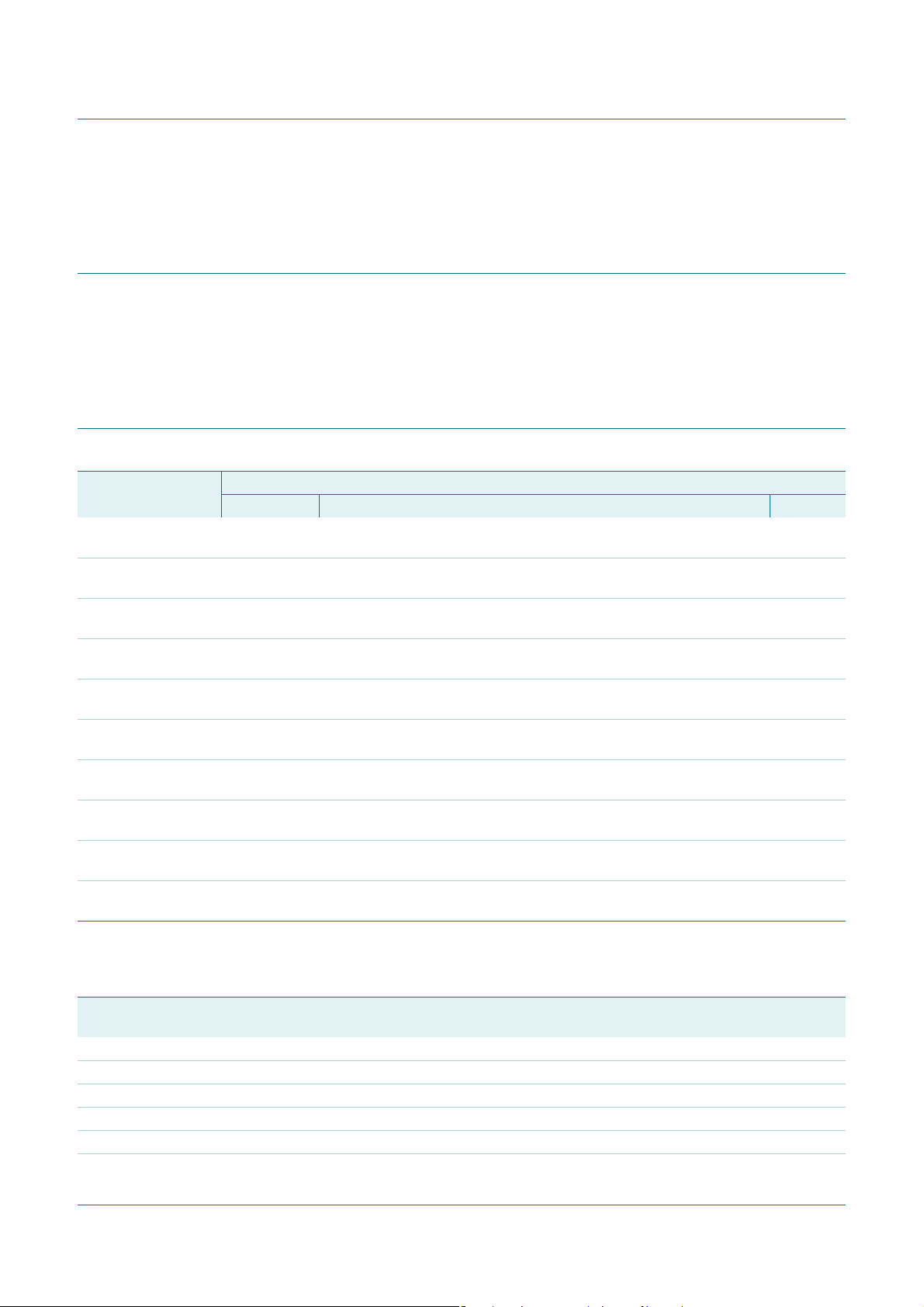
5. Block diagram
LPC1311/13/42/43
32-bit ARM Cortex-M3 microcontroller
GPIO ports
PIO0/1/2/3
RXD
TXD
DTR, DSR
DCD
CT32B0_MAT[3:0]
CT32B1_MAT[3:0]
CT16B0_MAT[2:0]
CT16B1_MAT[1:0]
(2)
, CTS,
(2)
(2)
, RI
, RTS
CT32B0_CAP0
CT32B1_CAP0
CT16B0_CAP0
CT16B1_CAP0
SWD
TEST/DEBUG
INTERFACE
ARM
CORTEX-M3
I-code
bus
HIGH-SPEED
GPIO
32-bit COUNTER/TIMER 0
32-bit COUNTER/TIMER 1
16-bit COUNTER/TIMER 0
16-bit COUNTER/TIMER 1
D-code
bus
UART
USB DEVICE
CONTROLLER
system
bus
AHB-LITE BUS
AHB TO
BRIDGE
USB pins
USB PHY
slaveslave
APB
LPC1311/13/42/43
(1)
WDO
POR
(1)
slave
WDT/WWDT
IRC
FLASH
8/16/32 kB
10-bit ADC
SSP0
SSP1
I2C-BUS
IOCONFIG
XTALIN
XTALOUT
CLOCK
GENERATION,
POWER CONTROL,
SYSTEM
FUNCTIONS
clocks and
controls
slave
slave
slave
(3)
(4)
RESET
CLKOUT
ROM
SRAM
4/8 kB
AD[7:0]
SCK0,SSEL0
MISO0, MOSI0
SCK1,SSEL1
MISO1, MOSI0
SCL
SDA
SYSTEM CONTROL
002aae722
(1) LPC1342/43 only.
(2) LQFP48 package only.
(3) On LPC1313FBD48/01 only.
(4) Windowed WatchDog Timer (WWDT) on LPC1311/01 and LPC1313/01 only.
Fig 1. Block diagram
LPC1311_13_42_43 All information provided in this document is subject to legal disclaimers. © NXP B.V. 2012. All rights reserved.
Product data sheet Rev. 5 — 6 June 2012 5 of 74
Page 6
NXP Semiconductors
6. Pinning information
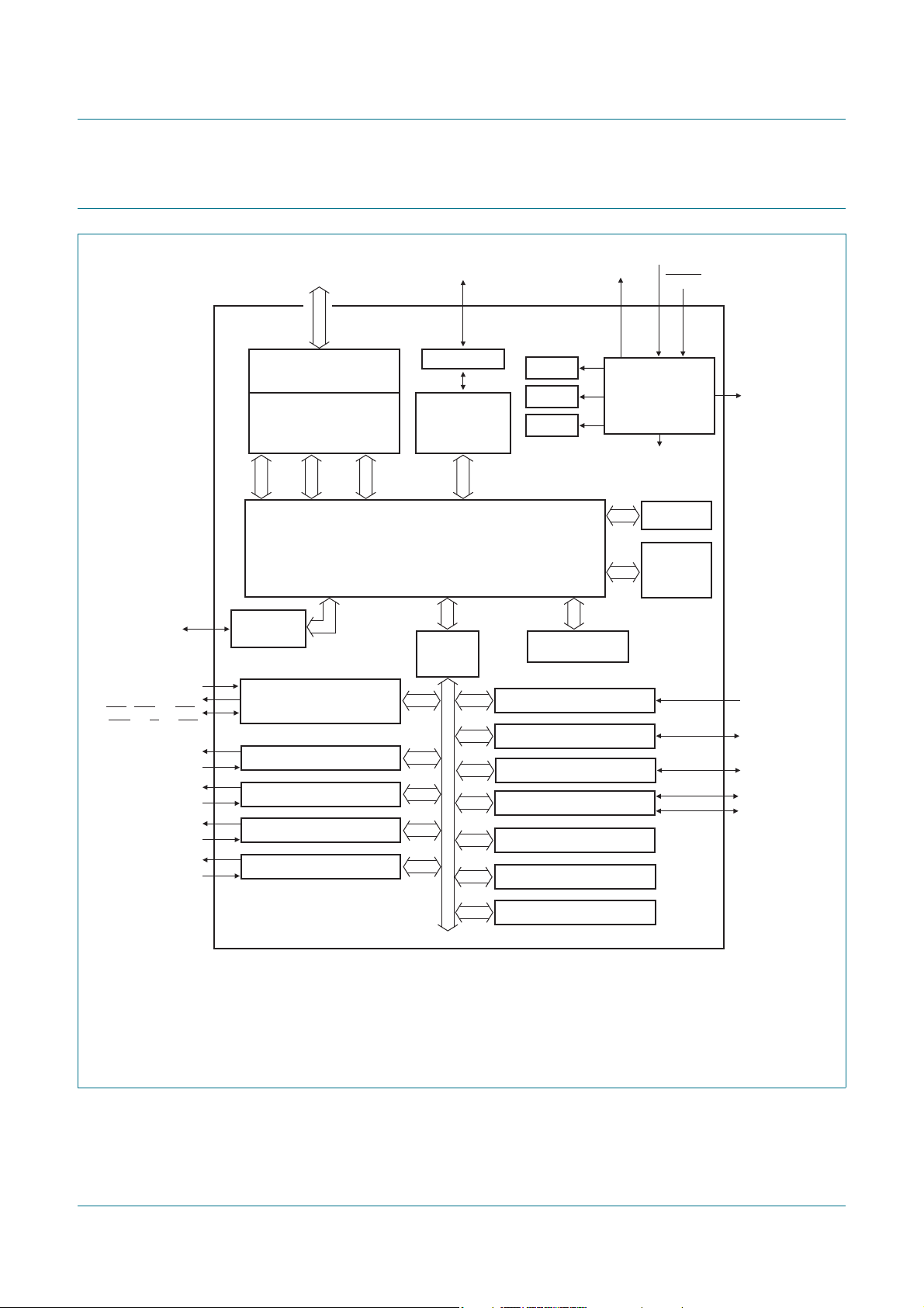
6.1 Pinning
LPC1311/13/42/43
32-bit ARM Cortex-M3 microcontroller
DD
4847464544434241403938
PIO2_6 PIO3_0
PIO2_0/DTR R/PIO1_2/AD3/CT32B1_MAT1
RESET/PIO0_0 R/PIO1_1/AD2/CT32B1_MAT0
PIO0_1/CLKOUT/CT32B0_MAT2/USB_FTOGGLE R/PIO1_0/AD1/CT32B1_CAP0
XTALIN PIO2_11/SCK0
XTALOUT PIO1_10/AD6/CT16B1_MAT1
PIO1_8/CT16B1_CAP0 PIO0_9/MOSI0/CT16B0_MAT1/SWO
PIO0_2/SSEL0/CT16B0_CAP0 PIO0_8/MISO0/CT16B0_MAT0
PIO2_7 PIO2_2/DCD
PIO2_8 PIO2_10
1
2
3
4
5
V
SS
6
7
8
V
DD
9
10
11
12
1314151617181920212223
PIO2_1/DSR PIO3_3
LPC1342FBD48
LPC1343FBD48
PIO0_4/SCL PIO1_6/RXD/CT32B0_MAT0
PIO0_5/SDA PIO1_5/RTS/CT32B0_CAP0
PIO0_3/USB_VBUS PIO1_7/TXD/CT32B0_MAT1
PIO1_9/CT16B1_MAT0 V
PIO2_4 PIO3_2
USB_DM PIO1_11/AD7
SS
USB_DP V
PIO2_3/RI
PIO3_1
37
36
35
34
33
32
R/PIO0_11/AD0/CT32B0_MAT3
31
30
29
SWCLK/PIO0_10/SCK0/CT16B0_MAT2
28
27
26
25
24
002aae505
PIO2_5 PIO1_4/AD5/CT32B1_MAT3/WAKEUP
PIO2_9
PIO0_7/CTS
PIO0_6/USB_CONNECT/SCK SWDIO/PIO1_3/AD4/CT32B1_MAT2
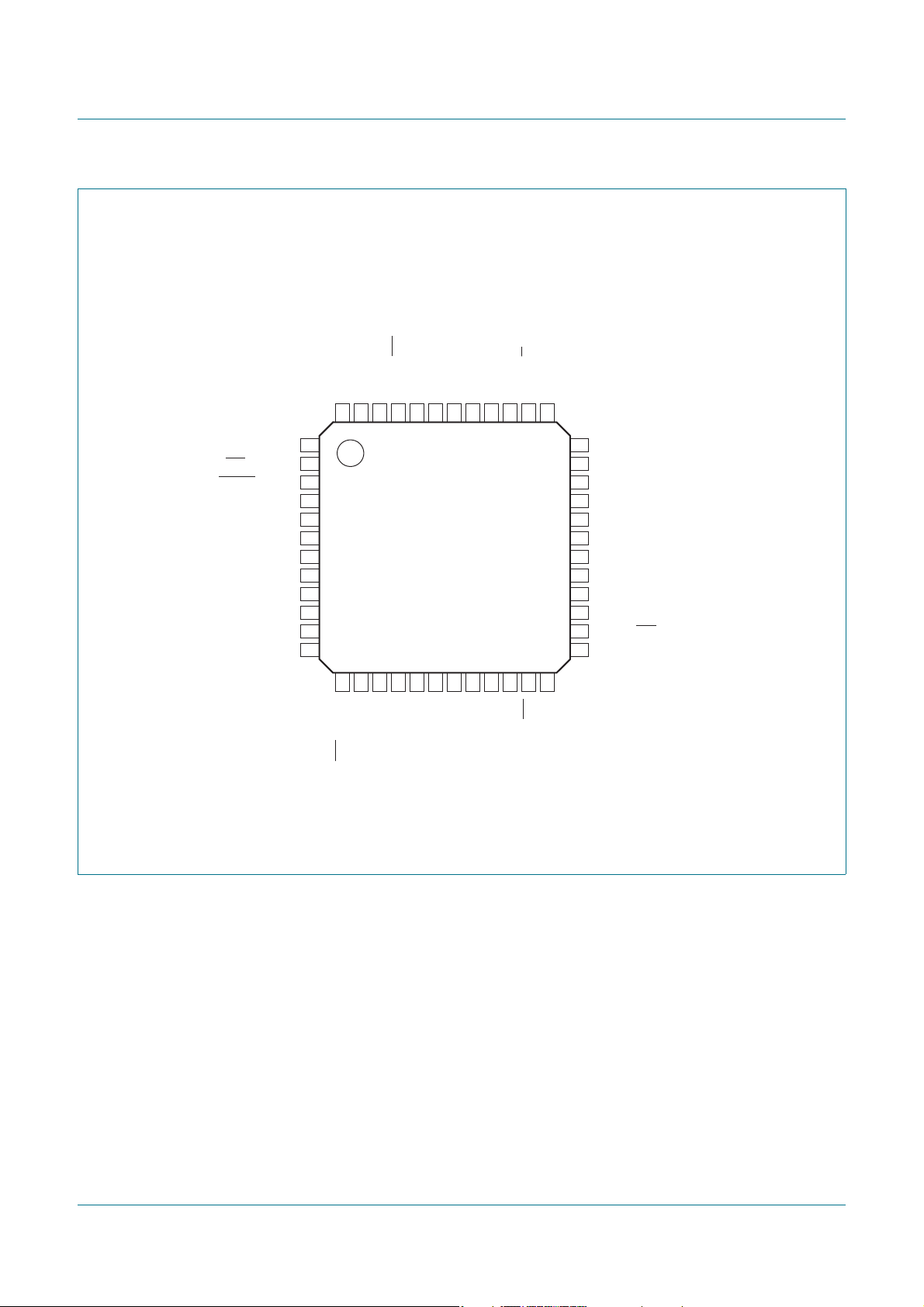
Fig 2. LPC1342/43 LQFP48 package
LPC1311_13_42_43 All information provided in this document is subject to legal disclaimers. © NXP B.V. 2012. All rights reserved.
Product data sheet Rev. 5 — 6 June 2012 6 of 74
Page 7
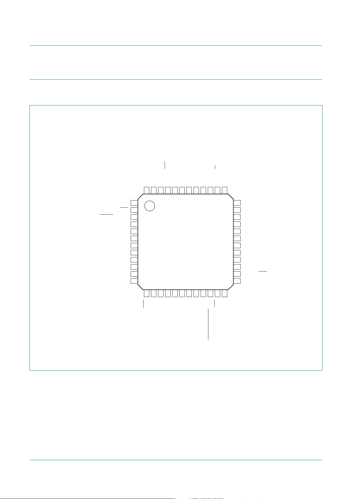
NXP Semiconductors
LPC1311/13/42/43
32-bit ARM Cortex-M3 microcontroller
terminal 1
index area
PIO2_0/DTR R/PIO1_2/AD3/CT32B1_MAT1
RESET/PIO0_0 R/PIO1_1/AD2/CT32B1_MAT0
PIO0_1/CLKOUT/CT32B0_MAT2/USB_FTOGGLE R/PIO1_0/AD1/CT32B1_CAP0
XTALOUT PIO1_10/AD6/CT16B1_MAT1
PIO1_8/CT16B1_CAP0
PIO0_2/SSEL0/CT16B0_CAP0
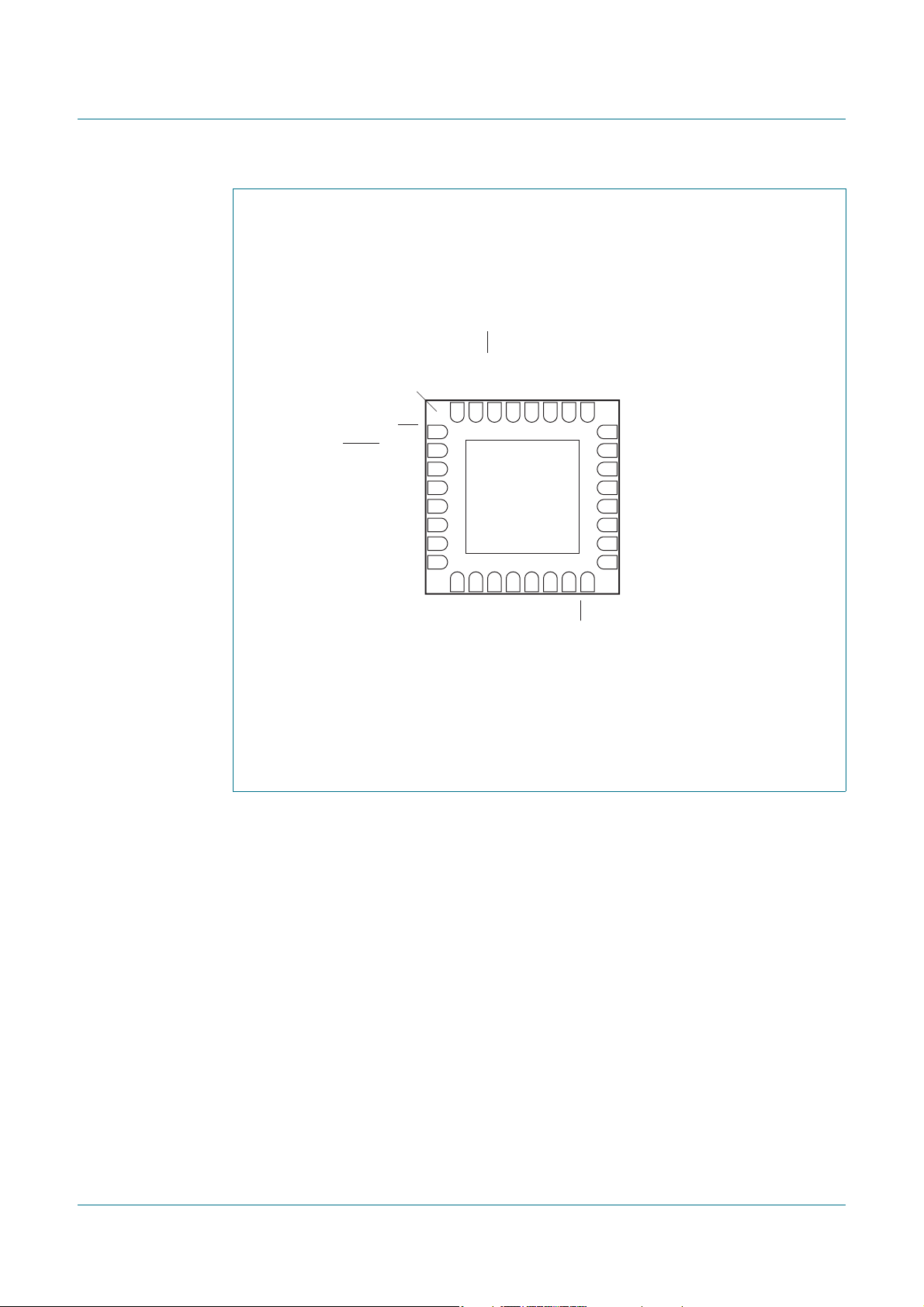
Fig 3. LPC1342/43 HVQFN33 package
DD
PIO3_2
PIO1_11/AD7
PIO1_4/AD5/CT32B1_MAT3/WAKEUP
PIO1_7/TXD/CT32B0_MAT1
PIO1_6/RXD/CT32B0_MAT0
PIO1_5/RTS/CT32B0_CAP0
V
32313029282726
1 24
2 23
3 22
XTALIN R/PIO0_11/AD0/CT32B0_MAT3
4 21
LPC1342FHN33
5 20
LPC1343FHN33
6 19
V
DD
7 18
8 17
33 V
SS
9
10111213141516
PIO0_4/SCL
PIO0_5/SDA
PIO0_3/USB_VBUS
PIO1_9/CT16B1_MAT0
Transparent top view
USB_DM
SWDIO/PIO1_3/AD4/CT32B1_MAT2
25
SWCLK/PIO0_10/SCK0/CT16B0_MAT2
PIO0_9/MOSI0/CT16B0_MAT1/SWO
PIO0_8/MISO0/CT16B0_MAT0
002aae516
USB_DP
PIO0_7/CTS
PIO0_6/USB_CONNECT/SCK0
LPC1311_13_42_43 All information provided in this document is subject to legal disclaimers. © NXP B.V. 2012. All rights reserved.
Product data sheet Rev. 5 — 6 June 2012 7 of 74
Page 8
NXP Semiconductors
LPC1311/13/42/43
32-bit ARM Cortex-M3 microcontroller
(1)
PIO3_3
4847464544434241403938
PIO2_6 PIO3_0
PIO2_0/DTR/SSEL1
RESET/PIO0_0 R/PIO1_1/AD2/CT32B1_MAT0
PIO0_1/CLKOUT/CT32B0_MAT2 R/PIO1_0/AD1/CT32B1_CAP0
XTALIN PIO2_11/SCK0
XTALOUT PIO1_10/AD6/CT16B1_MAT1
PIO1_8/CT16B1_CAP0 PIO0_9/MOSI0/CT16B0_MAT1/SWO
PIO0_2/SSEL0/CT16B0_CAP0 PIO0_8/MISO0/CT16B0_MAT0
PIO2_7 PIO2_2/DCD/MISO1
PIO2_8 PIO2_10
1
(1)
2
3
4
5
V
SS
6
7
8
V
DD
9
10
11
12
1314151617181920212223
(1)
PIO0_3 PIO1_7/TXD/CT32B0_MAT1
PIO2_1/DSR/SCK1
DD
LPC1313FBD48
LPC1313FBD48/01
PIO3_4 PIO3_2
PIO2_4 PIO1_11/AD7
PIO0_4/SCL PIO1_6/RXD/CT32B0_MAT0
PIO0_5/SDA PIO1_5/RTS/CT32B0_CAP0
PIO1_9/CT16B1_MAT0 V
PIO2_5 VSSPIO3_5 PIO1_4/AD5/CT32B1_MAT3/WAKEUP
PIO0_6/SCK0 SWDIO/PIO1_3/AD4/CT32B1_MAT2
PIO3_1
PIO2_3/RI/MOSI1
37
36
35
R/PIO1_2/AD3/CT32B1_MAT1
34
33
32
R/PIO0_11/AD0/CT32B0_MAT3
31
30
29
SWCLK/PIO0_10/SCK0/CT16B0_MAT2
28
27
26
25
24
002aae513
PIO2_9
PIO0_7/CTS
(1)
(1) SSP1 or UART function on LPC1313FBD48/01 only.
Fig 4. LPC1313 LQFP48 package
LPC1311_13_42_43 All information provided in this document is subject to legal disclaimers. © NXP B.V. 2012. All rights reserved.
Product data sheet Rev. 5 — 6 June 2012 8 of 74
Page 9
NXP Semiconductors
002aae517
LPC1311FHN33
LPC1311FHN33/01
LPC1313FHN33
LPC1313FHN33/01
Transparent top view
PIO0_8/MISO0/CT16B0_MAT0
PIO1_8/CT16B1_CAP0
PIO0_2/SSEL0/CT16B0_CAP0
PIO0_9/MOSI0/CT16B0_MAT1/SWO
V
DD
SWCLK/PIO0_10/SCK0/CT16B0_MAT2
XTALOUT PIO1_10/AD6/CT16B1_MAT1
XTALIN R/PIO0_11/AD0/CT32B0_MAT3
PIO0_1/CLKOUT/CT32B0_MAT2 R/PIO1_0/AD1/CT32B1_CAP0
RESET/PIO0_0 R/PIO1_1/AD2/CT32B1_MAT0
PIO2_0/DTR R/PIO1_2/AD3/CT32B1_MAT1
PIO0_3
PIO0_4/SCL
PIO0_5/SDA
PIO1_9/CT16B1_MAT0
PIO3_4
PIO3_5
PIO0_6/SCK0
PIO0_7/CTS
PIO1_7/TXD/CT32B0_MAT1
PIO1_6/RXD/CT32B0_MAT0
PIO1_5/RTS/CT32B0_CAP0
V
DD
PIO3_2
PIO1_11/AD7
PIO1_4/AD5/CT32B1_MAT3/WAKEUP
SWDIO/PIO1_3/AD4/CT32B1_MAT2
8 17
7 18
6 19
5 20
4 21
3 22
2 23
1 24
9
10111213141516
32313029282726
25
terminal 1
index area
33 V
SS
LPC1311/13/42/43
32-bit ARM Cortex-M3 microcontroller
Fig 5. LPC1311/13 HVQFN33 package
LPC1311_13_42_43 All information provided in this document is subject to legal disclaimers. © NXP B.V. 2012. All rights reserved.
Product data sheet Rev. 5 — 6 June 2012 9 of 74
Page 10
NXP Semiconductors
6.2 Pin description
Table 3. LPC1313/42/43 LQFP48 pin description table
Symbol Pin Start
/PIO0_0 3
RESET
PIO0_1/CLKOUT/
CT32B0_MAT2/
USB_FTOGGLE
PIO0_2/SSEL0/
CT16B0_CAP0
PIO0_3/USB_VBUS 14
PIO0_4/SCL 15
PIO0_5/SDA 16
PIO0_6/
USB_CONNECT
/
SCK0
PIO0_7/CTS
PIO0_8/MISO0/
CT16B0_MAT0
Type Reset
logic
input
[2]
yes I I; PU RESET — External reset input with 20 ns glitch filter. A LOW-going
state
[1]
Description
pulse as short as 50 ns on this pin resets the device, causing I/O
ports and peripherals to take on their default states, and processor
execution to begin at address 0.
I/O - PIO0_0 — General purpose digital input/output pin with 10 ns glitch
filter.
[3]
yes I/O I; PU PIO0_1 — General purpose digital input/output pin. A LOW level on
4
this pin during reset starts the ISP command handler or the USB
device enumeration (USB on LPC1342/43 only, see description of
PIO0_3).
O- CLKOUT — Clockout pin.
O- CT32B0_MAT2 — Match output 2 for 32-bit timer 0.
O- USB_FTOGGLE — USB 1 ms Start-of-Frame signal (LPC1342/43
only).
[3]
yes I/O I; PU PIO0_2 — General purpose digital input/output pin.
10
I/O - SSEL0 — Slave select for SSP0.
I- CT16B0_CAP0 — Capture input 0 for 16-bit timer 0.
[3]
yes I/O I; PU PIO0_3 — General purpose digital input/output pin. LPC1342/43
only: A LOW level on this pin during reset starts the ISP command
handler, a HIGH level starts the USB device enumeration.
I- USB_VBUS — Monitors the presence of USB bus power
(LPC1342/43 only).
[4]
yes I/O I; IA PIO0_4 — General purpose digital input/output pin (open-drain).
I/O - SCL — I
only if I
register.
[4]
yes I/O I; IA PIO0_5 — General purpose digital input/output pin (open-drain).
I/O - SDA — I
only if I
register.
[3]
22
yes I/O I; PU PIO0_6 — General purpose digital input/output pin.
O- USB_CONNECT
resistor under software control. Used with the SoftConnect USB
feature (LPC1342/43 only).
I/O - SCK0 — Serial clock for SSP0.
[3]
23
yes I/O I; PU PIO0_7 — General purpose digital input/output pin (high-current
output driver).
I- CTS
[3]
yes I/O I; PU PIO0_8 — General purpose digital input/output pin.
27
I/O - MISO0 — Master In Slave Out for SSP0.
O- CT16B0_MAT0 — Match output 0 for 16-bit timer 0.
LPC1311/13/42/43
32-bit ARM Cortex-M3 microcontroller
2
C-bus clock input/output (open-drain). High-current sink
2
C Fast-mode Plus is selected in the I/O configuration
2
C-bus data input/output (open-drain). High-current sink
2
C Fast-mode Plus is selected in the I/O configuration
— Signal used to switch an external 1.5 kΩ
— Clear To Send input for UART.
LPC1311_13_42_43 All information provided in this document is subject to legal disclaimers. © NXP B.V. 2012. All rights reserved.
Product data sheet Rev. 5 — 6 June 2012 10 of 74
Page 11

NXP Semiconductors
LPC1311/13/42/43
32-bit ARM Cortex-M3 microcontroller
Table 3. LPC1313/42/43 LQFP48 pin description table
Symbol Pin Start
logic
input
PIO0_9/MOSI0/
[3]
28
yes I/O I; PU PIO0_9 — General purpose digital input/output pin.
CT16B0_MAT1/
SWO
Type Reset
Description
state
[1]
I/O - MOSI0 — Master Out Slave In for SSP0.
O- CT16B0_MAT1 — Match output 1 for 16-bit timer 0.
O- SWO — Serial wire trace output.
[3]
SWCLK/PIO0_10/
SCK0/CT16B0_MAT2
yes I I; PU SWCLK — Serial wire clock.
29
I/O - PIO0_10 — General purpose dig ital input/ou tput pin.
I/O - SCK0 — Serial clock for SSP0.
O- CT16B0_MAT2 — Match output 2 for 16-bit timer 0.
[5]
R/PIO0_11/
AD0/CT32B0_MAT3
yes - I; PU R — Reserved. Configure for an alternate function in the IOCONFIG
32
block.
I/O - PIO0_11 — General purpose digital input/output pin.
I- AD0 — A/D converter, input 0.
O- CT32B0_MAT3 — Match output 3 for 32-bit timer 0.
[5]
R/PIO1_0/
AD1/CT32B1_CAP0
yes - I; PU R — Reserved. Configure for an alternate function in the IOCONFIG
33
block.
I/O - PIO1_0 — General purpose digital input/output pin.
I- AD1 — A/D converter, input 1.
I- CT32B1_CAP0 — Capture input 0 for 32-bit timer 1.
[5]
R/PIO1_1/
AD2/CT32B1_MAT0
yes - I; PU R — Reserved. Configure for an alternate function in the IOCONFIG
34
block.
I/O - PIO1_1 — General purpose digital input/output pin.
I- AD2 — A/D converter, input 2.
O- CT32B1_MAT0 — Match output 0 for 32-bit timer 1.
[5]
R/PIO1_2/
AD3/CT32B1_MAT1
yes - I; PU R — Reserved. Configure for an alternate function in the IOCONFIG
35
block.
I/O - PIO1_2 — General purpose digital input/output pin.
I- AD3 — A/D converter, input 3.
O- CT32B1_MAT1 — Match output 1 for 32-bit timer 1.
[5]
SWDIO/PIO1_3/
AD4/
CT32B1_MAT2
yes I/O I; PU SWDIO — Serial wire debug input/output.
39
I/O - PIO1_3 — General purpose digital input/output pin.
I- AD4 — A/D converter, input 4.
O- CT32B1_MAT2 — Match output 2 for 32-bit timer 1.
[5]
PIO1_4/AD5/
yes I/O I; PU PIO1_4 — General purpose digital input/output pin.
40
CT32B1_MAT3/
WAKEUP
I- AD5 — A/D converter, input 5.
O- CT32B1_MAT3 — Match output 3 for 32-bit timer 1.
I- WAKEUP — Deep power-down mode wake-up pin with 20 ns glitch
filter. This pin must be pulled HIGH externally to enter Deep
power-down mode and pulled LOW to exit Deep power-down mode.
A LOW-going pulse as short as 50 ns wakes up the part.
…continued
LPC1311_13_42_43 All information provided in this document is subject to legal disclaimers. © NXP B.V. 2012. All rights reserved.
Product data sheet Rev. 5 — 6 June 2012 11 of 74
Page 12
NXP Semiconductors
LPC1311/13/42/43
32-bit ARM Cortex-M3 microcontroller
Table 3. LPC1313/42/43 LQFP48 pin description table
Symbol Pin Start
logic
input
PIO1_5/RTS/
[3]
45
yes I/O I; PU PIO1_5 — General purpose digital input/output pin.
CT32B0_CAP0
Type Reset
Description
state
[1]
O- RTS
I- CT32B0_CAP0 — Capture input 0 for 32-bit timer 0.
[3]
PIO1_6/RXD/
CT32B0_MAT0
yes I/O I; PU PIO1_6 — General purpose digital input/output pin.
46
I- RXD — Receiver input for UART.
O- CT32B0_MAT0 — Match output 0 for 32-bit timer 0.
[3]
PIO1_7/TXD/
CT32B0_MAT1
yes I/O I; PU PIO1_7 — General purpose digital input/output pin.
47
O- TXD — Transmitter output for UART.
O- CT32B0_MAT1 — Match output 1 for 32-bit timer 0.
[3]
PIO1_8/CT16B1_CAP0 9
yes I/O I; PU PIO1_8 — General purpose digital input/output pin.
I- CT16B1_CAP0 — Capture input 0 for 16-bit timer 1.
[3]
PIO1_9/CT16B1_MAT0 17
yes I/O I; PU PIO1_9 — General purpose digital input/output pin.
O- CT16B1_MAT0 — Match output 0 for 16-bit timer 1.
[5]
PIO1_10/AD6/
CT16B1_MAT1
yes I/O I; PU PIO1_10 — General purpose dig ital input/ou tput pin.
30
I- AD6 — A/D converter, input 6.
O- CT16B1_MAT1 — Match output 1 for 16-bit timer 1.
[5]
PIO1_11/AD7 42
yes I/O I; PU PIO1_11 — General purpose digital input/output pin.
I- AD7 — A/D converter, input 7.
PIO2_0/DTR
/SSEL1 2
[3]
yes I/O I; PU PIO2_0 — General purpose digital input/output pin.
O- DTR
I/O - SSEL1 — Slave Select for SSP1 (LPC1313FBD48/01 only).
PIO2_1/DSR
/SCK1 13
[3]
yes I/O I; PU PIO2_1 — General purpose digital input/output pin.
I- DSR
I/O - SCK1 — Serial clock for SSP1 (LPC1313FBD48/01 only).
PIO2_2/DCD
/MISO1 26
[3]
yes I/O I; PU PIO2_2 — General purpose digital input/output pin.
I- DCD
I/O - MISO1 — Master In Slave Out for SSP1 (LPC1313FBD48/01 only).
PIO2_3/RI
/MOSI1 38
[3]
yes I/O I; PU PIO2_3 — General purpose digital input/output pin.
I- RI
— Ring Indicator input for UART.
I/O - MOSI1 — Master Out Slave In for SSP1 (LPC1313FBD48/01 only).
[3]
PIO2_4 18
yes I/O I; PU PIO2_4 — General purpose digital input/output pin (LPC1342/43
only).
[3]
PIO2_4 19
PIO2_5 21
yes I/O I; PU PIO2_4 — General purpose digital input/output pin (LPC1313 only).
[3]
yes I/O I; PU PIO2_5 — General purpose digital input/output pin (LPC1342/43
only).
[3]
PIO2_5 20
PIO2_6 1
PIO2_7 11
PIO2_8 12
PIO2_9 24
yes I/O I; PU PIO2_5 — General purpose digital input/output pin (LPC1313 only).
[3]
yes I/O I; PU PIO2_6 — General purpose digital input/output pin.
[3]
yes I/O I; PU PIO2_7 — General purpose digital input/output pin.
[3]
yes I/O I; PU PIO2_8 — General purpose digital input/output pin.
[3]
yes I/O I; PU PIO2_9 — General purpose digital input/output pin.
…continued
— Request To Send output for UART.
— Data Terminal Ready output for UART.
— Data Set Ready input for UART.
— Data Carrier Detect input for UART.
LPC1311_13_42_43 All information provided in this document is subject to legal disclaimers. © NXP B.V. 2012. All rights reserved.
Product data sheet Rev. 5 — 6 June 2012 12 of 74
Page 13
NXP Semiconductors
LPC1311/13/42/43
32-bit ARM Cortex-M3 microcontroller
Table 3. LPC1313/42/43 LQFP48 pin description table
Symbol Pin Start
logic
input
PIO2_10 25
PIO2_11/SCK0 31
[3]
yes I/O I; PU PIO2_10 — General purpose dig ital input/ou tput pin.
[3]
yes I/O I; PU PIO2_11 — General purpose digital input/output pin.
Type Reset
state
[1]
Description
I/O - SCK0 — Serial clock for SSP0.
[3]
36
PIO3_0/DTR
yes I/O I; PU PIO3_0 — General purpose digital input/output pin.
O- DTR
LPC1313/01 only).
[3]
37
PIO3_1/DSR
yes I/O I; PU PIO3_1 — General purpose digital input/output pin.
I- DSR
LPC1313/01 only).
[3]
43
PIO3_2/DCD
yes I/O I; PU PIO3_2 — General purpose digital input/output pin.
I- DCD
LPC1313/01 only).
[3]
48
PIO3_3/RI
yes I/O I; PU PIO3_3 — General purpose digital input/output pin.
I- RI
— Ring Indicator input for UART (LPC1311/01 and LPC1313/01
only).
[3]
PIO3_4 18
PIO3_5 21
USB_DM 19
USB_DP 20
V
DD
no I/O I; PU PIO3_4 — General purpose digital input/output pin (LPC1313 only).
[3]
no I/O I; PU PIO3_5 — General purpose digital input/output pin (LPC1313 only).
[6]
no I/O F USB_DM — USB bidirectional D− line (LPC1342/43 on ly).
[6]
no I/O F USB_DP — USB bidirectional D+ line (LPC1342/43 only).
8; 44- I - 3.3 V supply voltage to the internal regulator, the external rail, and
the ADC. Also used as the ADC reference voltage.
[7]
XTALIN 6
- I - Input to the oscillator circuit and internal clock generator circuits.
Input voltage must not exceed 1.8 V.
[7]
XTALOUT 7
V
SS
- O - Output from the oscillator amplifier.
5; 41- I - Ground.
…continued
— Data Terminal Ready output for UART (LPC1311/01 and
— Data Set Ready input for UART (LPC1311/01 and
— Data Carrier Detect input for UART (LPC1311/01 an d
[1] Pin state at reset for default function: I = Input; O = Output; PU = internal pull-up enabled (for VDD = 3.3 V, pin is pulled up to 2.6 V for
parts LPC1311/13/42/43 and pulled up to 3.3 V for parts LPC1311/01 and LPC1313/01); IA = inactive, no pull-up/down enabled;
F = floating; floating pins, if not used, should be tied to ground or power to minimize power consumption.
[2] 5 V tolerant pad. See Figure 37
WAKEUP pin to reset the chip and wake up from Deep power-down mode. An external pull-up resistor is required on this pin for the
Deep power-down mode.
[3] 5 V tolerant pad providing digital I/O functions with configurable pull-up/pull-down resistors and configurable hysteresis (see Figure 36
2
C-bus pads compliant with the I2C-bus specification for I2C standard mode and I2C Fast-mode Plus.
[4] I
[5] 5 V tolerant pad providing digital I/O functions with configurable pull-up/pull-down resistors, configurable hysteresis, and analog input.
When configured as a ADC input, digital section of the pad is disabled and the pin is not 5 V tolerant (see Figure 36
[6] Pad provides USB functions. It is designed in accordance with the USB specification, revision 2.0 (Full-speed and Low-speed mode
only). This pad is not 5 V tolerant.
[7] When the system oscillator is not used, connect XTALIN and XTALOUT as follows: XTALIN can be left floating or can be grounded
(grounding is preferred to reduce susceptibility to noise). XTALOUT should be left floating.
LPC1311_13_42_43 All information provided in this document is subject to legal disclaimers. © NXP B.V. 2012. All rights reserved.
Product data sheet Rev. 5 — 6 June 2012 13 of 74
for pad characteristics. RESET functionality is not available in Deep power-down mode. Use the
).
).
Page 14

NXP Semiconductors
LPC1311/13/42/43
32-bit ARM Cortex-M3 microcontroller
Table 4. LPC1311/13/42/43 HVQFN33 pin description table
Symbol Pin Start
/PIO0_0 2
RESET
Type Reset
logic
input
[2]
yes I I; PU RESET — External reset input with 20 ns glitch filter. A LOW-going pulse
state
[1]
Description
as short as 50 ns on this pin resets the device, causing I/O ports and
peripherals to take on their default states, and processor execution to
begin at address 0.
I/O - PIO0_0 — General purpose digital input/output pin with 10 ns glitch filter.
[3]
PIO0_1/CLKOUT/
CT32B0_MAT2/
USB_FTOGGLE
yes I/O I; PU PIO0_1 — General purpose digital input/output pin. A LOW level on this
3
pin during reset starts the ISP command handler or the USB device
enumeration (USB on LPC1342/43 only, see description of PIO0_3).
O- CLKOUT — Clock out pin.
O- CT32B0_MAT2 — Match output 2 for 32-bit timer 0.
O- USB_FTOGGLE — USB 1 ms Start-of-Frame signal (LPC1342/43 only).
[3]
PIO0_2/SSEL0/
CT16B0_CAP0
yes I/O I; PU PIO0_2 — General purpose digital input/output pin.
8
I/O - SSEL0 — Slave select for SSP0.
I- CT16B0_CAP0 — Capture input 0 for 16-bit timer 0.
[3]
PIO0_3/
USB_VBUS
yes I/O I; PU PIO0_3 — General purpose digital input/output pin. LPC1342/43 only: A
9
LOW level on this pin during reset starts the ISP command handler, a
HIGH level starts the USB device enumeration.
I- USB_VBUS — Monitors the presence of USB bus power (LPC1342/43
only).
[4]
PIO0_4/SCL 10
PIO0_5/SDA 11
PIO0_6/
USB_CONNECT
/
SCK0
yes I/O I; IA PIO0_4 — General purpose digital input/output pin (open-drain).
2
I/O - SCL — I
2
C Fast-mode Plus is selected in the I/O configuration register.
I
[4]
yes I/O I; IA PIO0_5 — General purpose digital input/output pin (open-drain).
I/O - SDA — I
2
C Fast-mode Plus is selected in the I/O configuration register.
I
[3]
15
yes I/O I; PU PIO0_6 — General purpose digital input/output pin.
C-bus clock input/output (open-drain). High-current sink only if
2
C-bus data input/output (open-drain). High-current sink only if
O- USB_CONNECT
under software control. Used with the SoftConnect USB feature
(LPC1342/43 only).
I/O - SCK0 — Serial clock for SSP0.
[3]
16
PIO0_7/CTS
yes I/O I; PU PIO0_7 — General purpose digital input/output pin (high-current output
driver).
— Clear To Send input for UART.
PIO0_8/MISO0/
CT16B0_MAT0
I- CTS
[3]
yes I/O I; PU PIO0_8 — General purpose digital input/output pin.
17
I/O - MISO0 — Master In Slave Out for SSP0.
O- CT16B0_MAT0 — Match output 0 for 16-bit timer 0.
[3]
PIO0_9/MOSI0/
CT16B0_MAT1/
SWO
yes I/O I; PU PIO0_9 — General purpose digital input/output pin.
18
I/O - MOSI0 — Master Out Slave In for SSP0.
O- CT16B0_MAT1 — Match output 1 for 16-bit timer 0.
O- SWO — Serial wire trace output.
— Signal used to switch an external 1.5 kΩ resistor
LPC1311_13_42_43 All information provided in this document is subject to legal disclaimers. © NXP B.V. 2012. All rights reserved.
Product data sheet Rev. 5 — 6 June 2012 14 of 74
Page 15

NXP Semiconductors
LPC1311/13/42/43
32-bit ARM Cortex-M3 microcontroller
Table 4. LPC1311/13/42/43 HVQFN33 pin description table
Symbol Pin Start
SWCLK/PIO0_10/
19
[3]
SCK0/
CT16B0_MAT2
logic
input
Type Reset
state
[1]
Description
yes I I; PU SWCLK — Serial wire clock.
I/O - PIO0_10 — General purpose digital input/output pin.
I/O - SCK0 — Serial clock for SSP0.
O- CT16B0_MAT2 — Match output 2 for 16-bit timer 0.
[5]
R/PIO0_11/AD0/
CT32B0_MAT3
yes - I; PU R — Reserved. Configure for an alternate function in the IOCONFIG
21
block.
I/O - PIO0_11 — General purpose digital input/output pin.
I- AD0 — A/D converter, input 0.
O- CT32B0_MAT3 — Match output 3 for 32-bit timer 0.
[5]
R/PIO1_0/AD1/
CT32B1_CAP0
yes - I; PU R — Reserved. Configure for an alternate function in the IOCONFIG
22
block.
I/O - PIO1_0 — General purpose digital input/output pin.
I- AD1 — A/D converter, input 1.
I- CT32B1_CAP0 — Capture input 0 for 32-bit timer 1.
[5]
R/PIO1_1/AD2/
CT32B1_MAT0
yes - I; PU R — Reserved. Configure for an alternate function in the IOCONFIG
23
block.
I/O - PIO1_1 — General purpose digital input/output pin.
I- AD2 — A/D converter, input 2.
O- CT32B1_MAT0 — Match output 0 for 32-bit timer 1.
[5]
R/PIO1_2/AD3/
CT32B1_MAT1
yes - I; PU R — Reserved. Configure for an alternate function in the IOCONFIG
24
block.
I/O - PIO1_2 — General purpose digital input/output pin.
I- AD3 — A/D converter, input 3.
O- CT32B1_MAT1 — Match output 1 for 32-bit timer 1.
[5]
SWDIO/PIO1_3/
AD4/
CT32B1_MAT2
yes I/O I; PU SWDIO — Serial wire debug input/output.
25
I/O - PIO1_3 — General purpose digital input/output pin.
I- AD4 — A/D converter, input 4.
O- CT32B1_MAT2 — Match output 2 for 32-bit timer 1.
[5]
PIO1_4/AD5/
CT32B1_MAT3/
WAKEUP
yes I/O I; PU PIO1_4 — General purpose digital input/output pin.
26
I- AD5 — A/D converter, input 5.
O- CT32B1_MAT3 — Match output 3 for 32-bit timer 1.
I- WAKEUP — Deep power-down mode wake-up pin with 20 ns glitch filter.
This pin must be pulled HIGH externally to enter Deep power-down mode
and pulled LOW to exit Deep power-down mode. A LOW-going pulse as
short as 50 ns wakes up the part.
PIO1_5/RTS
/
CT32B0_CAP0
[3]
30
yes I/O I; PU PIO1_5 — General purpose digital input/output pin.
O- RTS
— Request To Send output for UART.
I- CT32B0_CAP0 — Capture input 0 for 32-bit timer 0.
[3]
PIO1_6/RXD/
CT32B0_MAT0
yes I/O I; PU PIO1_6 — General purpose digital input/output pin.
31
I- RXD — Receiver input for UART.
O- CT32B0_MAT0 — Match output 0 for 32-bit timer 0.
…continued
LPC1311_13_42_43 All information provided in this document is subject to legal disclaimers. © NXP B.V. 2012. All rights reserved.
Product data sheet Rev. 5 — 6 June 2012 15 of 74
Page 16
NXP Semiconductors
LPC1311/13/42/43
32-bit ARM Cortex-M3 microcontroller
Table 4. LPC1311/13/42/43 HVQFN33 pin description table
Symbol Pin Start
PIO1_7/TXD/
32
[3]
CT32B0_MAT1
logic
input
Type Reset
state
[1]
Description
yes I/O I; PU PIO1_7 — General purpose digital input/output pin.
O- TXD — Transmitter output for UART.
O- CT32B0_MAT1 — Match output 1 for 32-bit timer 0.
[3]
PIO1_8/
CT16B1_CAP0
PIO1_9/
CT16B1_MAT0
PIO1_10/AD6/
CT16B1_MAT1
yes I/O I; PU PIO1_8 — General purpose digital input/output pin.
7
I- CT16B1_CAP0 — Capture input 0 for 16-bit timer 1.
[3]
yes I/O I; PU PIO1_9 — General purpose digital input/output pin.
12
O- CT16B1_MAT0 — Match output 0 for 16-bit timer 1.
[5]
yes I/O I; PU PIO1_10 — General purpose digital input/output pin.
20
I- AD6 — A/D converter, input 6.
O- CT16B1_MAT1 — Match output 1 for 16-bit timer 1.
[5]
PIO1_11/AD7 27
yes I/O I; PU PIO1_11 — General purpose digital input/output pin.
I- AD7 — A/D converter, input 7.
[3]
1
PIO2_0/DTR
PIO3_2 28
PIO3_4 13
PIO3_5 14
USB_DM 13
USB_DP 14
V
DD
yes I/O I; PU PIO2_0 — General purpose digital input/output pin.
O- DTR
[3]
yes I/O I; PU PIO3_2 — General purpose digital input/output pin.
[3]
no I/O I; PU PIO3_4 — General purpose digital input/output pin (LPC1311/13 only).
[3]
no I/O I; PU PIO3_5 — General purpose digital input/output pin (LPC1311/13 only).
[6]
no I/O F USB_DM — USB bidirectional D− line (LPC1342/43 only).
[6]
no I/O F USB_DP — USB bidirectional D+ line (LPC1342/43 only).
— Data Terminal Ready output for UART.
6; 29- I - 3.3 V supply voltage to the internal regulator, the external rail, and the
ADC. Also used as the ADC reference voltage.
[7]
XTALIN 4
- I - Input to the oscillator circuit and internal clock generator circuits. Input
voltage must not exceed 1.8 V.
[7]
XTALOUT 5
V
SS
- O - O utput from the oscillator amplifier.
33 - - - Thermal pad. Connect to ground.
…continued
[1] Pin state at reset for default function: I = Input; O = Output; PU = internal pull-up enabled (for VDD = 3.3 V, pin is pulled up to 2.6 V for
parts LPC1311/13/42/43 and pulled up to 3.3 V for parts LPC1311/01 and LPC1313/01); IA = inactive, no pull-up/down enabled.
F = floating; floating pins, if not used, should be tied to ground or power to minimize power consumption.
[2] 5 V tolerant pad. See Figure 37
WAKEUP pin to reset the chip and wake up from Deep power-down mode. An external pull-up resistor is required on this pin for the
Deep power-down mode.
[3] 5 V tolerant pad providing digital I/O functions with configurable pull-up/pull-down resistors and configurable hysteresis (see Figure 36
2
[4] I
C-bus pads compliant with the I2C-bus specification for I2C standard mode and I2C Fast-mode Plus.
[5] 5 V tolerant pad providing digital I/O functions with configurable pull-up/pull-down resistors, configurable hysteresis, and analog input.
When configured as a ADC input, digital section of the pad is disabled, and the pin is not 5 V tolerant (see Figure 36
[6] Pad provides USB functions. It is designed in accordance with the USB specification, revision 2.0 (Full-speed and Low-speed mode
only). This pad is not 5 V tolerant.
[7] When the system oscillator is not used, connect XTALIN and XTALOUT as follows: XTALIN can be left floating or can be grounded
(grounding is preferred to reduce susceptibility to noise). XTALOUT should be left floating.
LPC1311_13_42_43 All information provided in this document is subject to legal disclaimers. © NXP B.V. 2012. All rights reserved.
Product data sheet Rev. 5 — 6 June 2012 16 of 74
for pad characteristics. RESET functionality is not available in Deep power-down mode. Use the
).
).
Page 17

NXP Semiconductors
7. Functional description
7.1 Architectural overview
The ARM Cortex-M3 includes three AHB-Lite buses: the system bus, the I-code bus, and
the D-code bus (see Figure 1
system bus and are used similarly to TCM interfaces: one bus dedicated for instruction
fetch (I-code) and one bus for data access (D-c ode). The use of two core buses allows for
simultaneous operations if concurrent operations target different devices.
7.2 ARM Cortex-M3 processor
The ARM Cortex-M3 is a general purpose, 32-bit microprocessor, which offers high
performance and very low power consumption. The ARM Cortex-M3 offers ma ny new
features, including a Thumb-2 instruction set, low interrupt latency, hardware multiply and
divide, interruptible/continuable multiple load and store instructions, automatic state save
and restore for interrupts, tightly integrated interrupt controller, and multiple core buses
capable of simultaneous accesses.
LPC1311/13/42/43
32-bit ARM Cortex-M3 microcontroller
). The I-code and D-code core buses are faster than the
Pipeline techniques are employed so that all pa rts of the p rocessing and memory systems
can operate continuously. Typically, while one instruction is being executed, its successor
is being decoded, and a third instruction is being fetched from memory.
The ARM Cortex-M3 processor is described in detail in the Cortex-M3 Technical
Reference Manual which is available on the official ARM website.
7.3 On-chip flash program memory
The LPC1311/13/42/43 contain 32 kB (LPC1313 and LPC1343), 16 kB (LPC1342), or
8 kB (LPC1311) of on-chip flash memory.
7.4 On-chip SRAM
The LPC131 1/13/42/43 cont ain a total of 8 kB (LPC1343 and LPC1313) or 4 kB (L PC1342
and LPC1311) on-chip static RAM memory.
7.5 Memory map
The LPC1311/13/42/43 incorporate several distinct memory regions. Figure 6 shows the
overall map of the entire address space from the user program viewpoint following reset.
The interrupt vector area supports address remapping.
The AHB peripheral area is 2 MB in size and is divided to allow for up to 128 peripherals.
The APB peripheral area is 512 kB in size and is divided to allow for up to 32 peripherals.
Each peripheral of either type is allocated 16 kB of space. This allows simplifying the
address decoding for each peripheral.
LPC1311_13_42_43 All information provided in this document is subject to legal disclaimers. © NXP B.V. 2012. All rights reserved.
Product data sheet Rev. 5 — 6 June 2012 17 of 74
Page 18
NXP Semiconductors
LPC1311/13/42/43
32-bit ARM Cortex-M3 microcontroller
4 GB
1 GB
0.5 GB
I-code/D-code
memory space
0 GB
LPC1311/13/42/43
reserved
private peripheral bus
reserved
AHB peripherals
reserved
APB peripherals
reserved
reserved
16 kB boot ROM
reserved
8 kB SRAM (LPC1313/1343)
4 kB SRAM (LPC1311/1342)
reserved
32 kB on-chip flash (LPC1313/43)
16 kB on-chip flash (LPC1342)
8 kB on-chip flash (LPC1311)
0xFFFF FFFF
0xE010 0000
0xE000 0000
0x5020 0000
0x5000 0000
0x4008 0000
0x4000 0000
0x2000 0000
0x1FFF 4000
0x1FFF 0000
0x1000 2000
0x1000 1000
0x1000 0000
0x0000 8000
0x0000 4000
0x0000 2000
0x0000 0000
+ 256 words
active interrupt vectors
AHB peripherals
16 - 127 reserved
12-15
8-11
4-7
0-3
22
18
17
16
15
14
9
8
7
6
5
4
3
2
1
0
GPIO PIO3
GPIO PIO2
GPIO PIO1
GPIO PIO0
APB peripherals
23 - 31 reserved
SSP1 (LPC1313FBD48/01)
19 - 21 reserved
system control
IOCONFIG
SSP0
flash controller
PMU
10 - 13 reserved
reserved
USB (LPC1342/43 only)
ADC
32-bit counter/timer 1
32-bit counter/timer 0
16-bit counter/timer 1
16-bit counter/timer 0
UART
WDT/WWDT
2
C-bus
I
0x0000 0400
0x0000 0000
0x5020 0000
0x5004 0000
0x5003 0000
0x5002 0000
0x5001 0000
0x5000 0000
0x4008 0000
0x4005 C000
0x4005 8000
0x4004 C000
0x4004 8000
0x4004 4000
0x4004 0000
0x4003 C000
0x4003 8000
0x4002 8000
0x4002 4000
0x4002 0000
0x4001 C000
0x4001 8000
0x4001 4000
0x4001 0000
0x4000 C000
0x4000 8000
0x4000 4000
0x4000 0000
002aae723
Fig 6. LPC1311/13/42/43 memory map
7.6 Nested Vectored Interrupt Controller (NVIC)
The Nested Vectored Interrupt Controller (NVIC) is an integral part of the Cortex-M3. The
tight coupling to the CPU allows for low interrupt latency and efficient processing of late
arriving interrupts.
LPC1311_13_42_43 All information provided in this document is subject to legal disclaimers. © NXP B.V. 2012. All rights reserved.
Product data sheet Rev. 5 — 6 June 2012 18 of 74
Page 19

NXP Semiconductors
7.6.1 Features
• Controls system exceptions and peripheral interrupts.
• On the LPC1311/13/42/43, the NVIC supports up to 17 vectored interrupts. In
• 8 programmable interrupt priority levels, with hardware priority level masking
• Relocatable vector table.
• Software interrupt generation.
7.6.2 Interrupt sources
Each peripheral device has one interrupt line con nected to the NVIC but may have several
interrupt flags. Individual interrupt flags may also represent more than one interrupt
source.
Any GPIO pin (total of up to 42 pins) regardless of the selected function, can be
programmed to generate an interrupt on a level, or rising edge or falling edge, or both.
7.7 IOCONFIG block
LPC1311/13/42/43
32-bit ARM Cortex-M3 microcontroller
addition, up to 40 of the individual GPIO inputs are NVIC-vector capable.
The IOCONFIG block allows selected pins of the microcontroller to have more than one
function. Configuration registers control the multiplexers to allow connection between the
pin and the on-chip peripherals.
Peripherals should be connected to the appropriate pins prior to being activated and prior
to any related interrupt(s) being enabled. Activity of any enabled peripheral function that is
not mapped to a related pin should be considered undefined.
7.8 Fast general purpose parallel I/O
Device pins that are not connected to a specific peripheral function are controlled by the
GPIO registers. Pins may be dynamically configured as inputs or outputs. Multip le outputs
can be set or cleared in one write operation.
LPC1311/13/42/43 use accelerated GPIO functions:
• GPIO block is a dedicated AHB peripheral so that the fastest possible I/O timing can
be achieved.
• Entire port value can be written in one instruction.
Additionally, any GPIO pin (total of up to 42 pins) providing a digital function can be
programmed to generate an interrupt on a level, a rising or falling edge, or both.
7.8.1 Features
• Bit level port registers allow a single instruction to set or clear any number of bits in
one write operation.
• Direction control of individual bits.
• All I/O default to inputs with pull-up resistors enabled after reset with the exception of
2
the I
C-bus pins PIO0_4 and PIO0_5.
• Pull-up/pull-down resistor configuration can be programmed through the IOCONFIG
block for each GPIO pin.
LPC1311_13_42_43 All information provided in this document is subject to legal disclaimers. © NXP B.V. 2012. All rights reserved.
Product data sheet Rev. 5 — 6 June 2012 19 of 74
Page 20

NXP Semiconductors
• On the LPC1311/13/42/43, all GPIO pins (except PIO0_4 and PIO0_5) are pulled up
• On the LPC131 1/01 and LPC1313/01, all GPIO pins (except PIO0_4 and PIO0_5) ar e
7.9 USB interface (LPC1342/43 only)
The Universal Serial Bus (USB) is a 4-wire bus that supports communication between a
host and one or more (up to 127) peripherals. The host controller allocates the USB
bandwidth to attached devices through a token-based protocol. The bus supports
hot-plugging and dynamic configuration of the d evices. All transactions are initiated by the
host controller.
The LPC1342/43 USB interface is a device controller with on-chip PHY for device
functions.
7.9.1 Full-speed USB device controller
The device controller enables 12 Mbit/s data exchange with a USB Host controller. It
consists of a register interface, serial interface engine, and endpoint buffer memory. The
serial interface engine decodes the USB data stream and writes data to the appropriate
endpoint buffer. The status of a completed USB transfer or error condition is indicated via
status registers. An interrupt is also generated if enabled.
to 2.6 V (V
= 3.3 V) if their pull-up resistor is enabled in the IOCONFIG block.
DD
pulled up to 3.3 V (V
block.
LPC1311/13/42/43
32-bit ARM Cortex-M3 microcontroller
= 3.3 V) if their pull-up resistor is enabled in the IOCONFIG
DD
7.9.1.1 Features
• Dedicated USB PLL available.
• Fully compliant with USB 2.0 specification (full speed).
• Supports 10 physical (5 logical) endpoints with up to 64 bytes buffer RAM per
endpoint (see Table 5
• Supports Control, Bulk, Isochronous, and Interrupt endpoints.
• Supports SoftConnect feature.
• Double buffer implementation for Bulk and Isochronous endpoints.
Table 5. USB device endpoint configuration
Logical
endpoint
0 0 Control out 64 no
0 1 Control in 64 no
1 2 Interrupt/Bulk out 64 no
1 3 Interrupt/Bulk in 64 no
2 4 Interrupt/Bulk out 64 no
2 5 Interrupt/Bulk in 64 no
3 6 Interrupt/Bulk out 64 yes
3 7 Interrupt/Bulk in 64 yes
4 8 Isochronous out 512 yes
4 9 Isochronous in 512 yes
Physical
endpoint
).
Endpoint type Direction Packet size
(byte)
Double buffer
LPC1311_13_42_43 All information provided in this document is subject to legal disclaimers. © NXP B.V. 2012. All rights reserved.
Product data sheet Rev. 5 — 6 June 2012 20 of 74
Page 21

NXP Semiconductors
7.10 UART
The LPC1311/13/42/43 contains one UART.
Support for RS-485/9-bit mode allows both software addr ess detection and automatic
address detection using 9-bit mode.
The UART includes a fractional baud rate generator. Standard baud rates such as
115200 Bd can be achieved with any crystal frequency above 2 MHz.
7.10.1 Features
• Maximum UART data bit rate of 4.5 MBit/s.
• 16-byte receive and transmit FIFOs.
• Register locations conform to 16C550 industry standard .
• Receiver FIFO trigger points at 1 B, 4 B, 8 B, and 14 B.
• Built-in fractional baud rate generator covering wide range of baud rates without a
• Fractional divider for baud rate control, auto baud capabilities and FIFO control
• Support for RS-485/9-bit mode.
• Support for modem control.
LPC1311/13/42/43
32-bit ARM Cortex-M3 microcontroller
need for external crystals of particular values.
mechanism that enables software flow control implementation.
7.1 1 SSP serial I/O controller
The LPC1311/13/42/43 contain one SSP controller. An additional SSP controller is
available on the LPC1313FBD48/01 package.
The SSP controller is capable of operation on a SSP, 4-wire SSI, or Microwire bus. It can
interact with multiple masters and slaves on the bus. Only a single master and a single
slave can communicate on the bus during a given data transfer. The SSP supports full
duplex transfers, with frames of 4 bits to 16 bits of data flowing from the master to the
slave and from the slave to the master. In practice, often only one of these data flows
carries meaningful data.
7.11.1 Features
• Maximum SSP speed of 36 Mbit/s (master) or 6 Mbit/s (slave)
• Compatible with Motorola SPI, 4-wire Texas Instruments SSI, and National
Semiconductor Microwire buses
• Synchronous serial communication
• Master or slave operation
• 8-frame FIFOs for both transmit and receive
• 4-bit to 16-bit frame
7.12 I2C-bus serial I/O controller
The LPC1311/13/42/43 contain one I2C-bus controller.
LPC1311_13_42_43 All information provided in this document is subject to legal disclaimers. © NXP B.V. 2012. All rights reserved.
Product data sheet Rev. 5 — 6 June 2012 21 of 74
Page 22

NXP Semiconductors
The I2C-bus is bidirectional for inter-IC control using only two wires: a Serial Clock Line
(SCL) and a Serial DAta line (SDA). Each device is recognized by a unique address and
can operate as either a receiver-only device (e.g., an LCD driver) or a transmitter with the
capability to both receive and send information (such as memory). Transmitters and/or
receivers can operate in either master or sla ve mode, de pending o n whether the chip ha s
to initiate a data transfer or is only addressed. The I
controlled by more than one bus master connected to it.
7.12.1 Features
LPC1311/13/42/43
32-bit ARM Cortex-M3 microcontroller
2
C is a multi-master bus and can be
• The I
pins. The I
• Easy to configure as master, slave, or master/slave.
• Programmable clocks allow versatile rate control.
• Bidirectional data transfer between masters and slaves.
• Multi-master bus (no central master).
• Arbitration between simultaneously transmitting masters without corruption of serial
data on the bus.
• Serial clock synchronization allows devices with different bit rates to communicate via
one serial bus.
• Serial clock synchronization can be used as a handshake mechanism to suspend and
resume serial transfer.
• The I
• The I
7.13 10-bit ADC
The LPC1311/13/42/43 contains one ADC. It is a single 10-bit successive approximation
ADC with eight channels.
7.13.1 Features
2
C-bus interface is a standard I2C-bus compliant interface with true open-drain
2
C-bus interface also supports Fast-mode Plus with bit rates up to 1 Mbit/s.
2
C-bus can be used for test and diagnostic purposes.
2
C-bus controller supports multiple address recognition a nd a bus monitor mode.
• 10-bit successive approximation ADC.
• Input multiplexing among 8 pins.
• Power-down mode.
• Measurement range 0 V to V
DD
.
• 10-bit conversion time ≥ 2.44 μs (up to 400 kSamples/s).
• Burst conversion mode for single or multiple inputs.
• Optional conversion on transition of input pin or timer match signal.
• Individual result registers for each ADC channel to reduce interrupt overhead.
LPC1311_13_42_43 All information provided in this document is subject to legal disclaimers. © NXP B.V. 2012. All rights reserved.
Product data sheet Rev. 5 — 6 June 2012 22 of 74
Page 23

NXP Semiconductors
7.14 General purpose external event counter/timers
The LPC1311/13/42/43 includes two 32-bit counter/timers and two 16-bit counter/timers.
The counter/timer is designed to count cycles of the system derived clock. It can optionally
generate interrupts or perform other actions at specified timer values, based on four
match registers. Each counter/timer also includes one capture input to trap the timer value
when an input signal transitions, optionally generating an interrupt.
7.14.1 Features
• A 32-bit/16-bit counter/timer with a programmable 32-bit/16-bit prescaler.
• Counter or timer operation.
• One capture channel per timer , that can take a snapshot of the timer value when an
• Four match registers per timer that allow:
• Up to four external outputs corresponding to match registers, with the following
LPC1311/13/42/43
32-bit ARM Cortex-M3 microcontroller
input signal transitions. A capture event may also generate an interrupt.
– Continuous operation with optional interrupt generation on match.
– Stop timer on match with optional interrupt generation.
– Reset timer on match with optional interrupt generation.
capabilities:
– Set LOW on match.
– Set HIGH on match.
– Toggle on match.
– Do nothing on match.
7.15 System tick timer
The ARM Cortex-M3 includes a system tick timer (SYSTICK) that is intended to generate
a dedicated SYSTICK exception at a fixed time interval, normally set to 10 ms.
7.16 Watchdog timer
Remark: The standard Watchdog timer is available on parts LPC1311/13/42/43.
The purpose of the watchdog is to reset the microcontroller within a selectable time
period. When enabled, the watchdog will generate a system reset if the user program fails
to ‘feed’ (or reload) the watchdog within a predetermined amount of time.
7.16.1 Features
• Internally resets chip if not periodically reloaded.
• Debug mode.
• Enabled by software but requires a hardware reset or a watchdog reset/interrupt to be
disabled.
• Incorrect/incomplete feed sequence causes reset/interrupt if enabled.
• Flag to indicate watchdog reset.
• Programmable 24-bit timer with internal prescaler.
LPC1311_13_42_43 All information provided in this document is subject to legal disclaimers. © NXP B.V. 2012. All rights reserved.
Product data sheet Rev. 5 — 6 June 2012 23 of 74
Page 24

NXP Semiconductors
LPC1311/13/42/43
32-bit ARM Cortex-M3 microcontroller
• Selectable time period from (T
multiples of T
cy(WDCLK)
× 4.
cy(WDCLK)
• The Watchdog Clock (WDCLK) source can be selected from the Internal RC oscillator
(IRC), the watchdog oscillator, or the main clock. This gives a wide range of potential
timing choices of watchdog operation under different power reduction conditions. It
also provides the ability to run the WDT from an entirely internal source that is not
dependent on an external crystal and its associated components and wiring for
increased reliability.
7.17 Windowed WatchDog Timer (WWDT)
Remark: The windowed watchdog timer is available on parts LPC1311/01 and
LPC1313/01.
The purpose of the watchdog is to reset the controller if software fails to periodically
service it within a programmable time window.
7.17.1 Features
• Internally resets chip if not periodically reloaded during the programmable time-out
period.
• Optional windowed operation requires reload to occur between a minimum and
maximum time period, both programmable.
• Optional warning interrupt can be generated at a programmable time prior to
watchdog time-out.
• Enabled by software but requires a hardware reset or a watchdog reset/interrupt to be
disabled.
• Incorrect feed sequence causes reset or interrupt if enabled.
• Flag to indicate watchdog reset.
• Programmable 24-bit timer with internal prescaler.
• Selectable time period from (T
multiples of T
cy(WDCLK)
× 4.
cy(WDCLK)
• The Watchdog Clock (WDCLK) source can be selected from the IRC or the ded icated
watchdog oscillator (WDO). This gives a wide range of potential timing choices of
watchdog operation under different power conditions.
× 256 × 4) to (T
× 256 × 4) to (T
cy(WDCLK)
cy(WDCLK)
× 224× 4) in
× 224× 4) in
7.18 Clocking and power control
7.18.1 Integrated oscillators
The LPC1311/13/42/43 include three independent oscillators. These are the system
oscillator, the Internal RC oscillator (IRC), and the watchdog oscillator . Each oscillator can
be used for more than one purpose as required in a particular application.
Following reset, the LPC1311/13/42/43 will operate from the internal RC oscillator until
switched by software. This allows systems to operate without any external crystal and the
bootloader code to operate at a known frequency.
See Figure 7
LPC1311_13_42_43 All information provided in this document is subject to legal disclaimers. © NXP B.V. 2012. All rights reserved.
Product data sheet Rev. 5 — 6 June 2012 24 of 74
for an overview of the LPC1311/13/42/43 clock generation.
Page 25
NXP Semiconductors
IRC oscillator
watchdog oscillator
main clock
SYSTEM CLOCK
DIVIDER
LPC1311/13/42/43
32-bit ARM Cortex-M3 microcontroller
AHB clock 0
system clock
2
AHBCLKCTRL
(AHB clock enable)
AHBCLKCTRL
AHBCLKCTRL
SSP0/1 PERIPHERAL
CLOCK DIVIDER
UART PERIPHERAL
CLOCK DIVIDER
(system)
AHB clock 1
(ROM)
14
AHB clock 16
(IOCONFIG)
AHB clocks
2 to 15
(memories
and peripherals)
SSP0/1
UART
MAINCLKSEL
(main clock select)
IRC oscillator
SYSTEM PLL
system oscillator
SYSPLLCLKSEL
(system PLL clock select)
system oscillator
USBPLLCLKSEL
(USB clock select)
USB PLL
IRC oscillator
watchdog oscillator
(WDT clock update enable)
(USB clock update enable)
IRC oscillator
system oscillator
watchdog oscillator
The USB clock is available on LPC1342/43 only. SSP1 is available on LPC1313FBD48/01 only.
Fig 7. LPC1311/13/42/43 clocking generation block diagram
WDTUEN
USBUEN
CLKOUTUEN
(CLKOUT update enable)
ARM TRACE
CLOCK DIVIDER
SYSTICK TIMER
CLOCK DIVIDER
WDT CLOCK
DIVIDER
USB 48 MHz CLOCK
DIVIDER
CLKOUT PIN CLOCK
DIVIDER
ARM
trace clock
SYSTICK
timer
WDT
USB
CLKOUT pin
002aae859
7.18.1.1 Internal RC oscillator
The IRC may be used as the clock source for the WDT, and/or as the clock that drives the
system PLL and subsequently the CPU. The nominal IRC frequency is 12 MHz. The IRC
is trimmed to 1 % accuracy over the entire voltage and temperature range.
LPC1311_13_42_43 All information provided in this document is subject to legal disclaimers. © NXP B.V. 2012. All rights reserved.
Product data sheet Rev. 5 — 6 June 2012 25 of 74
Page 26

NXP Semiconductors
Upon power-up, any chip reset, or wake-up from Deep power-down mode, the
LPC1311/13/42/43 use the IRC as the clock source. Software may later switch to one of
the other available clock sources.
7.18.1.2 System oscillator
The system oscillator can be used as the clock source for the CPU, with or without using
the PLL. On the LPC1342/43, the system oscillator must be used to provide the clock
source to USB.
The system oscillator operates at frequencies of 1 MHz to 25 MHz. This frequency can be
boosted to a higher frequency, up to the maximum CPU operating frequency, by the
system PLL.
7.18.1.3 Watchdog oscillator
The watchdog oscillator can be used as a clock source that directly drives the CPU, the
watchdog timer, or the CLKOUT pin. The watchdog oscillator nominal frequency is
programmable between 7.8 kHz and 1.7 MHz. Th e frequency spre ad over processing and
temperature is ±40 % (see also Table 16
LPC1311/13/42/43
32-bit ARM Cortex-M3 microcontroller
).
7.18.2 System PLL and USB PLL
The LPC1342/43 contain a system PLL and a dedicated PLL for gener ating the 48 MHz
USB clock. The LPC131x contain the system PLL only. The system and USB PLLs are
identical.
The PLL accepts an input clock frequency in the range of 10 MHz to 25 MHz. The input
frequency is multiplied up to a high frequency with a Current Controlled Oscillator (CCO).
The multiplier can be an integer value from 1 to 32. The CCO operates in the range of
156 MHz to 320 MHz, so there is an additional divider in the loop to keep the CCO within
its frequency range while the PLL is providing the desired output frequency. The output
divider may be set to divide by 2, 4, 8, or 16 to produce the output clock. The PLL output
frequency must be lower than 100 MHz. Since the minimum output divider value is 2, it is
insured that the PLL output has a 50 % duty cycle. The PLL is turned off and bypassed
following a chip reset and may be enabled by software. The program must configure and
activate the PLL, wait for the PLL to lock, and then connect to the PLL as a clock source.
The PLL settling time is 100 μs.
7.18.3 Clock output
The LPC1311/13/42/43 features a clock output function that routes the IRC oscillator, the
system oscillator, the watchdog oscillator, or the main clock to an output pin.
7.18.4 Wake-up process
The LPC1311/13/42/43 begin operation at power-up and when awakened from Deep
power-down mode by using the 12 MHz IRC oscillator as the clock source. This allows
chip operation to resume quickly. If the main oscillator or the PLL is needed by the
application, software will need to enable these features and wait for them to stabilize
before they are used as a clock source.
LPC1311_13_42_43 All information provided in this document is subject to legal disclaimers. © NXP B.V. 2012. All rights reserved.
Product data sheet Rev. 5 — 6 June 2012 26 of 74
Page 27

NXP Semiconductors
7.18.5 Power control
The LPC1311/13/42/43 support a variety of power control features. There are three
special modes of processor power reduction: Sleep mode, Deep-sleep mode, and Deep
power-down mode. The CPU clock rate may also be controlled as needed by changing
clock sources, reconfiguring PLL values, and/or altering the CPU clock divide r value. This
allows a trade-off of power versus processing speed based on application requirements.
In addition, a register is provided for shutting down the clocks to individual on-chip
peripherals, allowing fine tuning of power consumption by eliminating all dynamic power
use in any peripherals that are not required for the app lication. Selected per ipher als have
their own clock divider which provides even better power control.
7.18.5.1 Power profiles (LPC1300L series, LPC1311/01 and LPC1313/01 only)
The power consumption in Active and Sleep modes can be optimized for the application
through simple calls to the power profile. The power configuration routine configures the
LPC1311/01 and the LPC1313/01 for one of the following power modes:
• Default mode corresponding to power configuration after reset.
• CPU performance mode corresponding to optimized processing capability.
• Efficiency mode corresponding to optim ized balance of current consumption and CPU
• Low-current mode corresponding to lowest power consumption.
LPC1311/13/42/43
32-bit ARM Cortex-M3 microcontroller
performance.
In addition, the power profile includes routines to select the optimal PLL settings for a
given system clock and PLL input clock.
7.18.5.2 Sleep mode
When Sleep mode is entered, the clock to the core is stopped. Resumption from the Sleep
mode does not need any special sequence but re-enabling the clock to the ARM core.
In Sleep mode, execution of instructions is suspended until either a reset or interrupt
occurs. Peripheral functions continue operation during Sleep mode and may generate
interrupts to cause the processor to resume execution. Sleep mode eliminates dynamic
power used by the processor itself, memory systems and related controllers, and internal
buses.
7.18.5.3 Deep-sleep mode
In Deep-sleep mode, the chip is in Sleep mode, and in addition all analog blocks are shut
down. As an exception, the user has the option to keep the watchdog oscillator and the
BOD circuit running for self-timed wake-up and BOD protection. Deep-sleep mode a llows
for additional power savings.
Up to 40 pins total can serve as external wake-up pins to the start logic to wake up the
chip from Deep-sleep mode (see Section 7.19.1
Unless the watchdog oscillator is selected to run in Deep-sleep mode, the clock source
should be switched to IRC before entering Deep-sleep mode, because the IRC can be
switched on and off glitch-free.
).
LPC1311_13_42_43 All information provided in this document is subject to legal disclaimers. © NXP B.V. 2012. All rights reserved.
Product data sheet Rev. 5 — 6 June 2012 27 of 74
Page 28

NXP Semiconductors
7.18.5.4 Deep power-down mode
In Deep power-down mode, power is shut off to the entire chip with the exception of the
WAKEUP pin. The LPC1311/13/42/43 can wake up from Deep power-down mode via the
WAKEUP pin.
A LOW-going pulse as short as 50 ns wakes up the part from Deep power-down mode.
When entering Deep power-down mode, an external pull-up resistor is required on the
WAKEUP pin to hold it HIGH. The RESET
floating while in Deep power-down mode.
7.19 System control
7.19.1 Start logic
The start logic connects external pins to corresponding interrupts in the NVIC. Each pin
shown in Table 3
NVIC interrupt vector table. The start logic pins can serve as external interrupt pins when
the chip is running. In addition, an input signal on the start logic pins can wake up the chip
from Deep-sleep mode when all clocks are shut down.
LPC1311/13/42/43
32-bit ARM Cortex-M3 microcontroller
pin must also be held HIGH to prevent it from
and Table 4 as input to the start logic has an individual interrupt in the
The start logic must be configured in the system configuration block and in the NVIC
before being used.
7.19.2 Reset
Reset has four sources on the LPC1311/13/42/43: the RESET pin, the Watchdog reset,
power-on reset (POR), and the Brown-Out Detection (BOD) circuit. The RESET
Schmitt trigger input pin. Assertion of chip reset by any source, once the operating voltage
attains a usable level, starts the IRC and initializes the flash controller.
When the internal reset is removed, the processor begins executing at address 0, which is
initially the reset vector mapped from the boot block. At that po int, all of the processor and
peripheral registers have been initialized to predetermined values.
7.19.3 Brownout detection
The LPC1311/13/42/43 includes four levels for monitoring the voltage on the VDD pin. If
this voltage falls below one of the four selected levels, the BOD asserts an interrupt signal
to the NVIC. This signal can be enabled for interrupt in the Interrupt Enable Register in the
NVIC in order to cause a CPU interrupt; if not, software can monitor the signal by reading
a dedicated status register. An additional threshold level can be selected to cause a
forced reset of the chip.
7.19.4 Code security (Code Read Protection - CRP)
This feature of the LPC1311/13/42/43 allows user to enable different levels of security in
the system so that access to the on-chip flash and use of the Serial Wire Debugger (SWD)
and In-System Programming (ISP) can be restricted. When needed, CRP is invoked by
programming a specific pattern into a dedicated flash location. In-Application
Programming (IAP) commands are not affected by the CRP.
pin is a
In addition, ISP entry via the PIO0_1 pin can be disabled without enabling CRP (NO_ISP
mode). For details see the LPC13xx user manual.
LPC1311_13_42_43 All information provided in this document is subject to legal disclaimers. © NXP B.V. 2012. All rights reserved.
Product data sheet Rev. 5 — 6 June 2012 28 of 74
Page 29
NXP Semiconductors
There are three levels of Code Read Protection:
1. CRP1 disables access to chip via the SWD and allows partial flash update (excluding
2. CRP2 disables access to chip via the SWD and only allows full flash era se and
3. Running an application with level CRP3 selected fully disables any access to chip via
CAUTION
LPC1311/13/42/43
32-bit ARM Cortex-M3 microcontroller
flash sector 0) using a limited set of the ISP commands. This mode is useful when
CRP is required and flash field updates are needed but all sectors can not be erased.
update using a reduced set of the ISP commands.
the SWD pins and the ISP. This mode effectively disables ISP override using PIO0_1
pin, too. It is up to the user’s application to provide (if needed) flash update
mechanism using IAP calls or call reinvoke ISP command to enable flash update via
UART.
If level three Code Read Protection (CRP3) is selected, no future factory testing can be
performed on the device.
7.19.5 Boot loader
The boot loader controls initial operation after reset and also provides the means to
program the flash memory. This could be initial programming of a blank device, erasure
and re-programming of a previously programmed device, or programming of the flash
memory by the application program in a running system.
The boot loader code is executed every time the part is reset or powered up. The loader
can either execute the ISP command handler or the user application code, or, on the
LPC1342/43, it can program the flash image via an att ached MSC device through USB
(Windows operating system only). A LOW level during reset applied to the PIO0_1 pin is
considered as an external hardware request to start th e ISP command handler or the USB
device enumeration. The state of PIO0_3 determ ines whether the UAR T or USB interface
will be used (LPC1342/43 only).
7.19.6 APB interface
The APB peripherals are located on one APB bus.
7.19.7 AHB-Lite
The AHB-Lite connects the instruction (I-code) and dat a (D-code) CPU bu ses o f the ARM
Cortex-M3 to the flash memory, the main static RAM, and the boot ROM.
7.19.8 External interrupt inputs
All GPIO pins can be level or edge sensitive interrupt inputs. In addition, start logic inputs
serve as external interrupts (see Section 7.19.1
).
7.19.9 Memory mapping control
The Cortex-M3 incorporates a mechanism that allows remapping the interrupt vector table
to alternate locations in the memory map. This is controlled via the Vector Table Offset
Register contained in the NVIC.
LPC1311_13_42_43 All information provided in this document is subject to legal disclaimers. © NXP B.V. 2012. All rights reserved.
Product data sheet Rev. 5 — 6 June 2012 29 of 74
Page 30

NXP Semiconductors
The vector table may be located anywhere within the bottom 1 GB of Cortex-M3 address
space. The vector table must be located on a 256 word bo undary.
7.20 Emulation and debugging
Debug functions are integrated into the ARM Cortex-M3. Serial wire debug is supported.
LPC1311/13/42/43
32-bit ARM Cortex-M3 microcontroller
LPC1311_13_42_43 All information provided in this document is subject to legal disclaimers. © NXP B.V. 2012. All rights reserved.
Product data sheet Rev. 5 — 6 June 2012 30 of 74
Page 31

NXP Semiconductors
8. Limiting values
LPC1311/13/42/43
32-bit ARM Cortex-M3 microcontroller
Table 6. Limiting values
In accordance with the Absolute Maximum Rating System (IEC 60134).
[1]
Symbol Parameter Conditions Min Max Unit
V
DD
supply voltage (core and
2.0 3.6 V
external rail)
V
I
input voltage 5 V tolerant I/O pins; only valid
[2]
−0.5 +5.5 V
when the VDD supply voltage is
present
I
DD
I
SS
I
latch
supply current per supply pin - 100 mA
ground current per ground pin - 100 mA
I/O latch-up current −(0.5VDD) < VI < (1.5VDD);
-100mA
Tj < 125 °C
T
stg
T
j(max)
P
tot(pack)
V
ESD
[1] The following applies to the limiting values:
a) This product includes circuitry specifically designed for the protection of its internal devices from the damaging effects of excessive
b) Parameters are valid over operating temperature range unless otherwise specified. All voltages are with respect to V
[2] Including voltage on outputs in 3-state mode.
[3] The maximum non-operating storage temperature is different than the temperature for required shelf life which should be determined
based on required shelf lifetime. Please refer to the JEDEC specification J-STD-033B.1 for further details.
[4] Human body model: equivalent to discharging a 100 pF capacitor through a 1.5 kΩ series resistor.
storage temperature non-operating
maximum junction temperature - 150 °C
total power dissipation (per
package)
based on package heat transfer, not
device power consumptio n
electrostatic discharge voltage human body model; all pins
static charge. Nonetheless, it is suggested that conventional precautions be taken to avoid applying greater than the rated
maximum.
otherwise noted.
[3]
−65 +150 °C
-1.5W
[4]
−6500 +6500 V
unless
SS
LPC1311_13_42_43 All information provided in this document is subject to legal disclaimers. © NXP B.V. 2012. All rights reserved.
Product data sheet Rev. 5 — 6 June 2012 31 of 74
Page 32

NXP Semiconductors
9. Static characteristics
LPC1311/13/42/43
32-bit ARM Cortex-M3 microcontroller
Table 7. Static characteristics
T
= −40 °C to +85 °C, unless otherwise specified.
amb
Symbol Parameter Conditions Min Typ
V
DD
supply voltage (core
[2]
2.0 3.3 3.6 V
and external rail)
LPC1300 series (LPC1311/13/42/43) power consumption
I
DD
supply current Active mode; VDD=3.3V;
T
=25°C; code
amb
while(1){}
executed from flash;
[3][4][5]
system clock = 12 MHz
system clock = 72 MHz
Sleep mode;
= 3.3 V; T
V
DD
amb
=25°C;
-4-mA
[6][7]
[4][5][6]
-17-mA
[8][7]
[3][4][5]
-2-mA
[6][7]
system clock = 12 MHz
Deep-sleep mode; V
T
=25°C
amb
= 3.3 V;
DD
Deep power-down mode;
V
DD
=3.3V; T
amb
=25°C
LPC1300L series (LPC1311/01, LPC1313/01) power consumption in low-current mode
I
DD
supply current Active mode; VDD=3.3V;
T
=25°C; code
amb
[4][9][7]
-30-μA
[10]
- 220 - nA
[11]
while(1){}
executed from flash;
[3][4][5]
-2-mA
[6][7]
[4][5][6]
-13-mA
[8][7]
[3][4][5]
-1-mA
[6][7]
[4][9][7]
-2-μA
[10]
- 220 - nA
-0.510nA
-0.510nA
-0.510nA
[12][13]
0- 5.0V
[14]
Standard port pins and RESET
I
IL
I
IH
LOW-level input current VI= 0 V; on-chip pull - up resi st or
HIGH-level input
current
I
OZ
OFF-state output
current
V
I
input voltage pin configured to provide a digital
system clock = 12 MHz
system clock = 72 MHz
Sleep mode;
= 3.3 V; T
V
DD
amb
=25°C;
system clock = 12 MHz
Deep-sleep mode; V
=25°C
T
amb
= 3.3 V;
DD
Deep power-down mode;
V
DD
=3.3V; T
amb
=25°C
pin; see Figure 21, Figure 22, Figure 23, Figure 24
disabled
VI=VDD; on-chip pull-down resistor
disabled
VO=0V; VO=VDD; on-chip
pull-up/down resistors disabled
function
[1]
Max Unit
LPC1311_13_42_43 All information provided in this document is subject to legal disclaimers. © NXP B.V. 2012. All rights reserved.
Product data sheet Rev. 5 — 6 June 2012 32 of 74
Page 33

NXP Semiconductors
LPC1311/13/42/43
32-bit ARM Cortex-M3 microcontroller
Table 7. Static characteristics
T
= −40 °C to +85 °C, unless otherwise specified.
amb
…continued
Symbol Parameter Conditions Min Typ
V
O
V
IH
output voltage output active 0 - V
HIGH-level input
0.7V
--V
DD
voltage
V
V
V
V
I
OH
I
OL
I
OHS
IL
hys
OH
OL
LOW-level input voltage - - 0.3V
hysteresis voltage 0.4 - - V
HIGH-level output
voltage
LOW-level output
voltage
HIGH-level output
current
LOW-level output
current
HIGH-level short-circuit
2.5 V ≤ V
2.0 V ≤ V
2.5 V ≤ V
2.0 V ≤ V
2.5 V≤ V
≤ 3.6 V; IOH= −4 mA VDD − 0.4--V
DD
< 2.5 V; IOH= −3 mA VDD − 0.4--V
DD
≤ 3.6 V; IOL=4 mA --0.4V
DD
< 2.5 V; IOL=3 mA --0.4V
DD
3.6 V;
DD ≤
VOH=VDD− 0.4 V
2.0 V ≤ V
V
OH=VDD
2.5 V ≤ V
2.0 V ≤ V
< 2.5 V;
DD
− 0.4 V
3.6 V; VOL=0.4V 4--mA
DD ≤
< 2.5 V; VOL=0.4V 3--mA
DD
VOH=0V
−4--mA
−3--mA
[15]
--−45 mA
output current
I
OLS
LOW-level short-circuit
VOL=V
DD
[15]
--50mA
output current
I
pd
I
pu
High-drive output pin (PIO0_7); see Figure 19
I
IL
pull-down current VI=5V 1050150μA
pull-up current VI=0V −15 −50 −85 μA
V
DD<VI
<5V 0 0 0 μA
and Figure 21
LOW-level input current VI= 0 V; on-chip pull - up resi st or
-0.510nA
disabled
I
IH
HIGH-level input
current
I
OZ
OFF-state output
current
V
I
V
O
V
IH
input voltage pin configured to provide a digital
output voltage output active 0 - V
HIGH-level input
VI=VDD; on-chip pull-down resistor
disabled
VO=0V; VO=VDD; on-chip
pull-up/down resistors disabled
function
-0.510nA
-0.510nA
[12][13]
0- 5.0V
[14]
0.7V
--V
DD
voltage
V
IL
V
hys
V
OH
V
OL
LOW-level input voltage - - 0.3V
hysteresis voltage 0.4 - - V
HIGH-level output
voltage
LOW-level output
voltage
2.5 V ≤ VDD ≤ 3.6 V; IOH= −20 mA VDD − 0.4--V
2.0 V ≤ V
< 2.5 V; IOH= −12 mA VDD − 0.4--V
DD
2.5 V ≤ VDD ≤ 3.6 V; IOL=4 mA --0.4V
2.0 V ≤ V
< 2.5 V; IOL=3 mA --0.4V
DD
[1]
Max Unit
DD
DD
V
V
V
V
DD
DD
LPC1311_13_42_43 All information provided in this document is subject to legal disclaimers. © NXP B.V. 2012. All rights reserved.
Product data sheet Rev. 5 — 6 June 2012 33 of 74
Page 34

NXP Semiconductors
LPC1311/13/42/43
32-bit ARM Cortex-M3 microcontroller
Table 7. Static characteristics
T
= −40 °C to +85 °C, unless otherwise specified.
amb
…continued
Symbol Parameter Conditions Min Typ
I
OH
HIGH-level output
current
2.5 V ≤ VDD ≤ 3.6 V;
VOH=VDD− 0.4 V
2.0 V ≤ V
< 2.5 V;
DD
20--mA
12--mA
VOH=VDD− 0.4 V;
I
OL
LOW-level output
current
I
pd
I
pu
2
C-bus pins (PIO0_4 and PIO0_5); see Figure 20
I
V
IH
pull-down current VI=5V 1050150μA
pull-up current VI=0V −15 −50 −85 μA
HIGH-level input
2.5 V ≤ VDD ≤ 3.6 V; VOL=0.4V 4--mA
2.0 V ≤ V
V
DD<VI
< 2.5 V; VOL=0.4V 3--mA
DD
<5V 0 0 0 μA
0.7V
--V
DD
voltage
V
IL
V
hys
I
OL
I
OL
LOW-level input voltage - - 0.3V
hysteresis voltage - 0.05V
LOW-level output
current
LOW-level output
current
VOL=0.4V; I2C-bus pins configured
as standard mode pins
2.5 V ≤ V
2.0 V ≤ V
≤ 3.6 V 3.5 - - mA
DD
< 2.5 V 3.0 - - mA
DD
VOL=0.4V; I2C-bus pins configured
as Fast-mode Plus pins
2.5 V ≤ VDD ≤ 3.6 V 20 - - mA
2.0 V ≤ V
I
LI
input leakage current VI=V
= 5 V - 10 22 μA
V
I
DD
< 2.5 V 16 - -
DD
[16]
-24μA
Oscillator pins
V
V
i(xtal)
o(xtal)
crystal input voltage −0.5 +1.8 +1.95 V
crystal output voltage −0.5 +1.8 +1.95 V
USB pins (LPC1342/43 only)
I
OZ
OFF-state output
0V<VI<3.3V
[17]
--±10 μA
current
V
BUS
V
DI
bus supply voltage
differential input
|(D+) − (D−)|
[17]
--5.25V
[17]
0.2--V
sensitivity voltage
V
CM
differential common
includes VDI range
[17]
0.8 - 2.5 V
mode voltage range
V
th(rs)se
single-ended receiver
[17]
0.8 - 2.0 V
switching threshold
voltage
V
OL
LOW-level output
voltage
for low-/full-speed;
of 1.5 kΩ to 3.6 V
R
L
[17]
--0.18V
[1]
Max Unit
DD
-V
DD
V
LPC1311_13_42_43 All information provided in this document is subject to legal disclaimers. © NXP B.V. 2012. All rights reserved.
Product data sheet Rev. 5 — 6 June 2012 34 of 74
Page 35

NXP Semiconductors
LPC1311/13/42/43
32-bit ARM Cortex-M3 microcontroller
Table 7. Static characteristics
T
= −40 °C to +85 °C, unless otherwise specified.
amb
Symbol Parameter Conditions Min Typ
V
OH
HIGH-level output
voltage
C
Z
trans
DRV
transceiver capacitance pin to GND
driver output
impedance for driver
…continued
driven; for low-/full-speed;
RL of 15 kΩ to GND
with 33 Ω series resistor; steady state
drive
[1]
[17]
2.8 - 3.5 V
[17]
--20pF
[18][17]
36 - 44.1 Ω
Max Unit
which is not high-speed
capable
[1] Typical ratings are not guaranteed. The values listed are at room temperature (25 °C), nominal supply voltages.
[2] For LPC1342 and LPC1343 only: For USB operation 3.0 V ≤ V
[3] IRC enabled; system oscillator disabled; system PLL disabled.
[4] I
measurements were performed with all pins configured as GPIO outputs driven LOW and pull-up resistors disabled.
DD
[5] BOD disabled.
[6] All peripherals disabled in the SYSAHBCLKCTRL register. Peripheral clocks to UART, SSP, trace clock, and SysTick timer disabled in
the syscon block.
[7] For LPC1342/43: USB_DP and USB_DM pulled LOW externally.
[8] IRC disabled; system oscillator enabled; system PLL enabled.
[9] All oscillators and analog blocks turned off in the PDSLEEPCFG register; PDSLEEPCFG = 0x0000 0FFF.
[10] WAKEUP pin pulled HIGH externally. An external pull-up resistor is required on the RESET
[11] Low-current mode PWR_LOW_CURRENT selected when running the set_power routine in the power profiles.
[12] Including voltage on outputs in 3-state mode.
[13] V
[14] 3-state outputs go into 3-state mode in Deep power-down mode.
[15] Allowed as long as the current limit does not exceed the maximum current allowed by the device.
[16] To V
[17] 3.0 V ≤ V
[18] Includes external resistors of 33 Ω±1 % on USB_DP and USB_DM.
supply voltage must be present.
DD
.
SS
≤ 3.6 V.
DD
≤ 3.6 V. Guaranteed by design.
DD
pin for the Deep power-down mode.
Table 8. ADC static characteristics
= −40 °C to +85 °C unless otherwise specified; ADC frequency 4.5 MHz, VDD = 2.5 V to 3.6 V.
T
amb
Symbol Parameter Conditions Min Typ Max Unit
V
C
E
E
E
E
E
R
IA
ia
D
L(adj)
O
G
T
vsi
analog input voltage 0 - V
DD
analog input capacitance - - 1 pF
differential linearity error
integral non-linearity
offset error
gain error
absolute error
voltage source interface
[1][2]
--±1LSB
[3]
--±1.5 LSB
[4]
--±3.5 LSB
[5]
--0.6%
[6]
--±4LSB
--40kΩ
V
resistance
R
i
[1] The ADC is monotonic, there are no missing codes.
[2] The differential linearity error (E
LPC1311_13_42_43 All information provided in this document is subject to legal disclaimers. © NXP B.V. 2012. All rights reserved.
Product data sheet Rev. 5 — 6 June 2012 35 of 74
input resistance
) is the difference between the actual step width and the ideal step width. See Figure 8.
D
[7][8]
--2.5MΩ
Page 36

NXP Semiconductors
LPC1311/13/42/43
32-bit ARM Cortex-M3 microcontroller
[3] The integral non-linearity (E
) is the peak difference between the center of the steps of the actual and the ideal transfer curve after
L(adj)
appropriate adjustment of gain and offset errors. See Figure 8
[4] The offset error (E
ideal curve. See Figure 8
[5] The gain error (E
) is the absolute difference between the straight line which fits the actual curve and the straight line which fits the
O
.
) is the relative difference in percent between the straight line fitting the actual transfer curve after removing offset
G
error, and the straight line which fits the ideal transfer curve. See Figure 8
[6] The absolute error (E
ADC and the ideal transfer curve. See Figure 8
[7] T
= 25 °C; maximum sampling frequency fs = 400 kSamples/s and analog input capacitance Cia = 1 pF.
amb
[8] Input resistance R
) is the maximum difference between the center of the steps of the actual transfer curve of the non-calibrated
T
.
depends on the sampling frequency fs: Ri = 1 / (fs × Cia).
i
.
.
LPC1311_13_42_43 All information provided in this document is subject to legal disclaimers. © NXP B.V. 2012. All rights reserved.
Product data sheet Rev. 5 — 6 June 2012 36 of 74
Page 37
NXP Semiconductors
002aaf426
1023
1022
1021
1020
1019
(2)
(1)
10241018 1019 1020 1021 1022 1023
7123456
7
6
5
4
3
2
1
0
1018
(5)
(4)
(3)
1 LSB
(ideal)
code
out
V
DD
− VSS
1024
offset
error
E
O
gain
error
E
G
offset error
E
O
VIA (LSB
ideal
)
1 LSB =
LPC1311/13/42/43
32-bit ARM Cortex-M3 microcontroller
(1) Example of an actual transfer curve.
(2) The ideal transfer curve.
(3) Differential linearity error (E
(4) Integral non-linearity (E
L(adj)
).
D
).
(5) Center of a step of the actual transfer curve.
Fig 8. ADC characteristics
LPC1311_13_42_43 All information provided in this document is subject to legal disclaimers. © NXP B.V. 2012. All rights reserved.
Product data sheet Rev. 5 — 6 June 2012 37 of 74
Page 38

NXP Semiconductors
9.1 BOD static characteristics for LPC1300 series
Remark: Applies to parts LPC1311/13/42/43 and all their packages.
Table 9. BOD static characteristics
T
amb
Symbol Parameter Conditions Min Typ Max Unit
V
th
LPC1311/13/42/43
32-bit ARM Cortex-M3 microcontroller
[1]
=25°C.
threshold voltage interrupt level 0
assertion - 1.69 - V
de-assertion - 1.84 - V
interrupt level 1
assertion - 2.29 - V
de-assertion - 2.44 - V
interrupt level 2
assertion - 2.59 - V
de-assertion - 2.74 - V
interrupt level 3
assertion - 2.87 - V
de-assertion - 2.98 - V
reset level 0
assertion - 1.49 - V
de-assertion - 1.64 - V
[1] Interrupt levels are selected by writing the level value to the BOD control register BODCTRL, see LPC13xx
user manual.
LPC1311_13_42_43 All information provided in this document is subject to legal disclaimers. © NXP B.V. 2012. All rights reserved.
Product data sheet Rev. 5 — 6 June 2012 38 of 74
Page 39

NXP Semiconductors
9.2 BOD static characteristics for LPC1300L series (LPC1311/01 and LPC1313/01)
Remark: Applies to parts LPC1311/01 and LPC1313/01 and all packages.
Table 10. BOD static characteristics
T
amb
Symbol Parameter Conditions Min Typ Max Unit
V
th
LPC1311/13/42/43
32-bit ARM Cortex-M3 microcontroller
[1]
=25°C.
threshold voltage interrupt level 0
assertion - 1.65 - V
de-assertion - 1.80 - V
interrupt level 1
assertion - 2.22 - V
de-assertion - 2.35 - V
interrupt level 2
assertion - 2.52 - V
de-assertion - 2.66 - V
interrupt level 3
assertion - 2.80 - V
de-assertion - 2.90 - V
reset level 0
assertion - 1.46 - V
de-assertion - 1.63 - V
reset level 1
assertion - 2.06 - V
de-assertion - 2.15 - V
reset level 2
assertion - 2.35 - V
de-assertion - 2.43 - V
reset level 3
assertion - 2.63 - V
de-assertion - 2.71 - V
[1] Interrupt levels are selected by writing the level value to the BOD control register BODCTRL, see LPC13xx
user manual.
9.3 Power consumption for LPC1300 series
Remark: Applies to parts LPC1311/13/42/43 and all their packages.
Power measurements in Active, Sleep, and Deep-sleep modes were performe d under the
following conditions (see LPC13xx user manual):
• Configure all pins as GPIO with pull-up resistor disabled in the IOCONFIG block.
• Configure GPIO pins as outputs using the GPIOnDIR registers.
• Write 0 to all GPIOnDATA registers to drive the outputs LOW.
LPC1311_13_42_43 All information provided in this document is subject to legal disclaimers. © NXP B.V. 2012. All rights reserved.
Product data sheet Rev. 5 — 6 June 2012 39 of 74
Page 40

NXP Semiconductors
VDD (V)
2.0 3.63.22.82.4
002aae993
9
12
6
15
18
I
DD
(mA)
3
24 MHz
48 MHz
12 MHz
36 MHz
72 MHz
002aae994
temperature (°C)
−40 853510 60−15
6
15
12
9
18
I
DD
(mA)
3
24 MHz
12 MHz
36 MHz
72 MHz
48 MHz
LPC1311/13/42/43
32-bit ARM Cortex-M3 microcontroller
Conditions: T
= 25 °C; Active mode entered executing code
amb
while(1){}
from flash;
internal pull-up resistors disabled; system oscillator and system PLL enabled; IRC, BOD disabled;
all peripherals disabled in the SYSAHBCLKCTRL register (SYSAHBCLKCTRL = 0x1F); all
peripheral clocks disabled; USB_DP and USB_DM pulled LOW externally (LPC1342/43).
Fig 9. Typical supply current versus regulator supply voltage VDD in Active mode
(LPC1311/13/42/43)
LPC1311_13_42_43 All information provided in this document is subject to legal disclaimers. © NXP B.V. 2012. All rights reserved.
Product data sheet Rev. 5 — 6 June 2012 40 of 74
Conditions: VDD = 3.3 V; Active mode entered executing code
while(1){}
from flash; internal
pull-up resistors disabled; system oscillator and system PLL enabled; IRC, BOD disabled; all
peripherals disabled in the SYSAHBCLKCTRL register (SYSAHBCLKCTRL = 0x1F); all peripheral
clocks disabled; USB_DP and USB_DM pulled LOW externally (LPC1342/43).
Fig 10. Typical supply current versus temperature in Active mode (LPC1311/13/42/43)
Page 41

NXP Semiconductors
002aae995
temperature (°C)
−40 853510 60−15
2
8
6
4
10
I
DD
(mA)
0
12 MHz
36 MHz
72 MHz
48 MHz
24 MHz
002aae998
temperature (°C)
−40 853510 60−15
20
60
40
80
I
DD
(μA)
0
VDD = 3.6 V
3.3 V
2.0 V
Fig 11. Typical supply current versus temperature in Sleep mode (LPC1311/13/42/43)
LPC1311/13/42/43
32-bit ARM Cortex-M3 microcontroller
Conditions: VDD = 3.3 V; Sleep mode entered from flash; internal pull-up resistors disabled; system
oscillator and system PLL enabled; IRC, BOD disabled; all peripherals disabled in the
SYSAHBCLKCTRL register (SYSAHBCLKCTRL = 0x1F); all peripheral clocks disabled; USB_DP
and USB_DM pulled LOW externally (LPC1342/43).
Conditions: BOD disabled; all oscillators and analog blocks turned off in the PDSLEEPCFG
register; PDSLEEPCFG = 0x0000 0FFF; USB_DP and USB_DM pulled LOW externally
(LPC1342/43).
LPC1311_13_42_43 All information provided in this document is subject to legal disclaimers. © NXP B.V. 2012. All rights reserved.
Product data sheet Rev. 5 — 6 June 2012 41 of 74
Fig 12. Typical supply current versus temperature in Deep-sleep mode (analog blocks
disabled; LPC1311/13/42/43)
Page 42

NXP Semiconductors
002aae996
0.4
0.6
1.2
I
DD
(μA)
0
temperature (°C)
−40 853510 60−15
VDD = 3.6 V
3.3 V
2.0 V
Fig 13. Typical supply current versus temperature in Deep power-down mode
LPC1311/13/42/43
32-bit ARM Cortex-M3 microcontroller
(LPC1311/13/42/43)
9.4 Power consumption for LPC1300L series (LPC1311/01 and LPC1313/01)
Remark: Applies to parts LPC1311/01 and LPC1313/01 and all their packages.
Power measurements in Active, Sleep, and Deep-sleep modes were performe d under the
following conditions (see LPC13xx user manual):
• Configure all pins as GPIO with pull-up resistor disabled in the IOCONFIG block.
• Configure GPIO pins as outputs using the GPIOnDIR registers.
• Write 0 to all GPIOnDATA registers to drive the outputs LOW.
LPC1311_13_42_43 All information provided in this document is subject to legal disclaimers. © NXP B.V. 2012. All rights reserved.
Product data sheet Rev. 5 — 6 June 2012 42 of 74
Page 43
NXP Semiconductors
LPC1311/13/42/43
32-bit ARM Cortex-M3 microcontroller
16
I
DD
(mA)
12
8
4
0
2.0 3.63.22.82.4
Conditions: T
72 MHz
48 MHz
36 MHz
24 MHz
12 MHz
= 25 °C; Active mode entered executing code
amb
while(1){}
002aag235
VDD (V)
from flash;
internal pull-up resistors disabled; system oscillator and system PLL enabled; IRC, BOD disabled;
all peripherals disabled in the SYSAHBCLKCTRL register (SYSAHBCLKCTRL = 0x1F); all
peripheral clocks disabled; low-current mode.
Fig 14. Typical supply current versus regulator supply voltage VDD in Active mode
(LPC1311/01 and LPC1313/01)
16
I
DD
(mA)
12
8
4
0
˗40 853510 60˗15
72 MHz
48 MHz
36 MHz
24 MHz
12 MHz
Conditions: VDD = 3.3 V; Active mode entered executing code
while(1){}
002aag236
temperature (°C)
from flash; internal
pull-up resistors disabled; system oscillator and system PLL enabled; IRC, BOD disabled; all
peripherals disabled in the SYSAHBCLKCTRL register (SYSAHBCLKCTRL = 0x1F); all peripheral
clocks disabled; low-current mode.
Fig 15. Typical supply current versus temperature in Active mode (LPC1311/01 and
LPC1313/01)
LPC1311_13_42_43 All information provided in this document is subject to legal disclaimers. © NXP B.V. 2012. All rights reserved.
Product data sheet Rev. 5 — 6 June 2012 43 of 74
Page 44

NXP Semiconductors
LPC1311/13/42/43
32-bit ARM Cortex-M3 microcontroller
8
I
DD
(mA)
6
4
2
0
˗40 853510 60˗15
72 MHz
48 MHz
36 MHz
24 MHz
12 MHz
002aag237
temperature (°C)
Conditions: VDD = 3.3 V; Sleep mode entered from flash; internal pull-up resistors disabled; system
oscillator and system PLL enabled; IRC, BOD disabled; all peripherals disabled in the
SYSAHBCLKCTRL register (SYSAHBCLKCTRL = 0x1F); all peripheral clocks disabled;
low-current mode.
Fig 16. Typical supply current versus temperature in Sleep mode (LPC1311/01 and
LPC1313/01)
8
I
DD
(μA)
6
4
2
0
˗40 853510 60˗15
VDD = 2.0 V
3.3 V
3.6 V
002aag238
temperature (°C)
Conditions: BOD disabled; all oscillators and analog blocks turned off in the PDSLEEPCFG
register; PDSLEEPCFG = 0x0000 0FFF.
Fig 17. Typical supply current versus temperature in Deep-sleep mode (analog blocks
disabled, LPC1311/01 and LPC1313/01)
LPC1311_13_42_43 All information provided in this document is subject to legal disclaimers. © NXP B.V. 2012. All rights reserved.
Product data sheet Rev. 5 — 6 June 2012 44 of 74
Page 45

NXP Semiconductors
LPC1311/13/42/43
32-bit ARM Cortex-M3 microcontroller
0.6
I
DD
(µA)
0.4
0.2
0
˗40 853510 60˗15
VDD = 3.6 V
3.3 V
2.0 V
002aag239
temperature (°C)
Fig 18. Typical supply current versus temperature in Deep power-down mode
(LPC1311/01 and LPC1313/01)
9.5 Peripheral power consumption
The supply current per peripheral is measured a s the difference in supply current between
the peripheral block enabled and the peripheral block disabled in the SYSAHBCLKCFG or
PDRUNCFG (for analog blocks) registers. All other blocks are disabled in both registers
and no code is executed. Measured on a typical sample at T
otherwise, the system oscillator and PLL are running in both measurements.
=25 °C. Unless noted
amb
The supply currents are shown for system clock frequencies of 12 MHz, 48 MHz, and
72 MHz.
Table 11. Power consumption for individual analog and digital blocks
Peripheral Typical supply current in mA Notes
n/a 12 MHz 48 MHz 72 MHz
IRC 0.23 - - - System oscillator running; PLL off; independent of main clock
System oscillator
at 12 MHz
Watchdog
oscillator at
500 kHz/2
BOD 0.045 - - - Independent of main clock frequency.
Main or USB PLL - 0.26 0.34 0.48 ADC - 0.07 0.25 0.37 CLKOUT - 0.14 0.56 0.82 Main clock divided by 4 in the CLKOUTDIV register.
CT16B0 - 0.01 0.05 0.08 CT16B1 - 0.01 0.04 0.06 CT32B0 - 0.01 0.05 0.07 CT32B1 - 0.01 0.04 0.06 -
frequency.
0.23 - - - IRC running; PLL off; independent of main clock frequency.
0.002 - - - System oscillator running; PLL off; independent of main clock
frequency.
LPC1311_13_42_43 All information provided in this document is subject to legal disclaimers. © NXP B.V. 2012. All rights reserved.
Product data sheet Rev. 5 — 6 June 2012 45 of 74
Page 46
NXP Semiconductors
IOH (mA)
0 60402010 5030
002aae990
2.8
2.4
3.2
3.6
V
OH
(V)
2
T = 85 °C
25 °C
−40 °C
LPC1311/13/42/43
32-bit ARM Cortex-M3 microcontroller
Table 11. Power consumption for individual analog and digital blocks
…continued
Peripheral Typical supply current in mA Notes
n/a 12 MHz 48 MHz 72 MHz
GPIO - 0.21 0.80 1.17 GPIO pins configu r ed as outputs and set to LOW. Direction
and pin state are maintained if the GPIO is disabled in the
SYSAHBCLKCFG register.
IOCONFIG - 0.00 0.02 0.02 I2C - 0.03 0.12 0.17 ROM - 0.04 0.15 0.22 SSP0 - 0.11 0.41 0.60 SSP1 - 0.11 0.41 0.60 On LPC1313FBD48/01 only.
UART - 0.20 0.76 1.11 WDT - 0.01 0.05 0.08 Main clock selected as clock source for the WDT.
USB - - 3.91 - Main clock selected as clock source for the USB. USB_DP
and USB_DM pulled LOW externally.
USB - 1.84 4.19 5.71 Ded icated USB PLL selected as clock source for the USB.
USB_DP and USB_DM pulled LOW externally.
9.6 Electrical pin characteristics
LPC1311_13_42_43 All information provided in this document is subject to legal disclaimers. © NXP B.V. 2012. All rights reserved.
Product data sheet Rev. 5 — 6 June 2012 46 of 74
Conditions: VDD = 3.3 V; on pin PIO0_7.
Fig 19. High - drive output: Typical HIGH-level output voltage VOH versus HIGH-level
output current IOH.
Page 47

NXP Semiconductors
VOL (V)
0 0.60.40.2
002aaf019
20
40
60
I
OL
(mA)
0
T = 85 °C
25 °C
−40 °C
VOL (V)
0 0.60.40.2
002aae991
5
10
15
I
OL
(mA)
0
T = 85 °C
25 °C
−40 °C
Fig 20. I2C-bus pins (high current sink): Typical LOW-level output current IOL versus
LPC1311/13/42/43
32-bit ARM Cortex-M3 microcontroller
Conditions: VDD = 3.3 V; on pins PIO0_4 and PIO0_5.
LOW-level output voltage VOL
Conditions: VDD = 3.3 V; standard port pins and PIO0_7.
Fig 21. Typical LOW-level output current IOL versus LOW-level output voltage VOL
LPC1311_13_42_43 All information provided in this document is subject to legal disclaimers. © NXP B.V. 2012. All rights reserved.
Product data sheet Rev. 5 — 6 June 2012 47 of 74
Page 48

NXP Semiconductors
IOH (mA)
0 24168
002aae992
2.8
2.4
3.2
3.6
V
OH
(V)
2
T = 85 °C
25 °C
−40 °C
VI (V)
0 54231
002aae988
−30
−50
−10
10
I
pu
(μA)
−70
T = 85 °C
25 °C
−40 °C
Fig 22. Typical HIGH-level output voltage VOH versus HIGH-level output source current
Conditions: VDD = 3.3 V; standard port pins.
I
OH
LPC1311/13/42/43
32-bit ARM Cortex-M3 microcontroller
Conditions: VDD = 3.3 V; standard port pins.
Fig 23. Typical pull-up current Ipu versus input voltage V
i
LPC1311_13_42_43 All information provided in this document is subject to legal disclaimers. © NXP B.V. 2012. All rights reserved.
Product data sheet Rev. 5 — 6 June 2012 48 of 74
Page 49
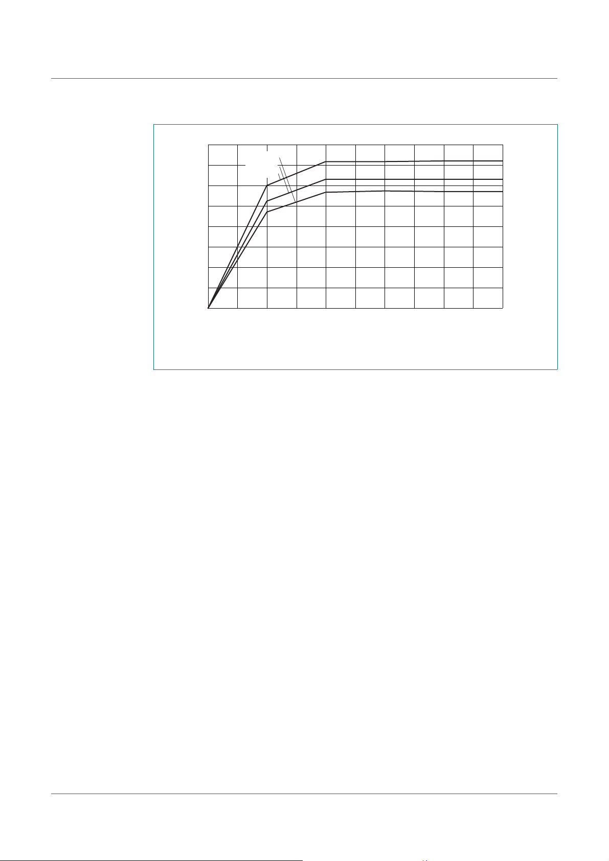
NXP Semiconductors
VI (V)
0 54231
002aae989
40
20
60
80
I
pd
(μA)
0
T = 85 °C
25 °C
−40 °C
Fig 24. Typical pull-down current Ipd versus input voltage V
LPC1311/13/42/43
32-bit ARM Cortex-M3 microcontroller
Conditions: VDD = 3.3 V; standard port pins.
i
LPC1311_13_42_43 All information provided in this document is subject to legal disclaimers. © NXP B.V. 2012. All rights reserved.
Product data sheet Rev. 5 — 6 June 2012 49 of 74
Page 50

NXP Semiconductors
V
DD
0
400 mV
t
r
t
wait
t = t
1
002aag001
10. Dynamic characteristics
10.1 Power-up ramp conditions
Table 12. Power-up characteristics
T
= −40 °C to +85 °C.
amb
Symbol Parameter Conditions Min Typ Max Unit
t
r
t
wait
V
I
[1] See Figure 25.
[2] The wait time specifies the time the power supply must be at levels below 400 mV before ramping up.
rise time at t = t1: 0 < VI ≤ 400 mV
wait time
input voltage at t = t1 on pin V
DD
LPC1311/13/42/43
32-bit ARM Cortex-M3 microcontroller
[1]
0- 500 ms
[1][2]
12 - - μs
0 - 400 mV
Condition: 0 < VI ≤ 400 mV at start of power-up (t = t1)
Fig 25. Power-up ramp
10.2 Flash memory
Table 13. Flash characteristics
T
= −40 °C to +85 °C, unless otherwise specified.
amb
Symbol Parameter Conditions Min Typ Max Unit
N
endu
t
ret
t
er
t
prog
[1] Number of program/erase cycles.
[2] Programming times are given for writing 256 bytes from RAM to the flash. Data must be written to the flash in blocks of 256 bytes.
LPC1311_13_42_43 All information provided in this document is subject to legal disclaimers. © NXP B.V. 2012. All rights reserved.
Product data sheet Rev. 5 — 6 June 2012 50 of 74
endurance
[1]
10000 100000 - cycles
retention time powered 10 - - years
unpowered 20 - - years
erase time sector or multiple
95 100 105 ms
consecutive sectors
programming time
[2]
0.95 1 1.05 ms
Page 51

NXP Semiconductors
t
CHCL
t
CLCX
t
CHCX
T
cy(clk)
t
CLCH
002aaa907
LPC1311/13/42/43
32-bit ARM Cortex-M3 microcontroller
10.3 External clock
Table 14. Dynamic characteristic: externa l clock
T
= −40 °C to +85 °C; VDD over specified ranges.
amb
Symbol Parameter Conditions Min Typ
f
osc
T
cy(clk)
t
CHCX
t
CLCX
t
CLCH
t
CHCL
[1] Parameters are valid over operating temperature range unless otherwise specified.
[2] Typical ratings are not guaranteed. The values listed are at room temperature (25 °C), nominal supply voltages.
[1]
[2]
oscillator frequency 1 - 25 MHz
clock cycle time 40 - 1000 ns
clock HIGH time T
clock LOW time T
× 0.4 - - ns
cy(clk)
× 0.4 - - ns
cy(clk)
clock rise time - - 5 ns
clock fall time - - 5 ns
Max Unit
Fig 26. E xternal clock timing (with an amplitude of at least V
i(RMS)
= 200 mV)
LPC1311_13_42_43 All information provided in this document is subject to legal disclaimers. © NXP B.V. 2012. All rights reserved.
Product data sheet Rev. 5 — 6 June 2012 51 of 74
Page 52

NXP Semiconductors
temperature (°C)
−40 853510 60−15
002aae987
11.95
12.05
12.15
f
(MHz)
11.85
V
DD
= 3.6 V
3.3 V
3.0 V
2.7 V
2.4 V
2.0 V
LPC1311/13/42/43
32-bit ARM Cortex-M3 microcontroller
10.4 Internal oscillators
Table 15. Dynamic characteristics: IRC
T
= −40 °C to +85 °C; 2.7 V ≤ V
amb
Symbol Parameter Conditions Min Typ
f
osc(RC)
[1] Parameters are valid over operating temperature range unless otherwise specified.
[2] Typical ratings are not guaranteed. The values listed are at room temperature (25 °C), nominal supply voltages.
DD
≤ 3.6 V
[1]
.
[2]
internal RC oscillator frequency - 11 .88 12 12.12 MHz
Max Unit
Conditions: Frequency values are typical values. 12 MHz ± 1 % accuracy is guaranteed for
2.7 V ≤ V
≤ 3.6 V and T
DD
= −40 °C to +85 °C. Variations between parts may cause the IRC to
amb
fall outside the 12 MHz ± 1 % accuracy specification for voltages below 2.7 V.
Fig 27. Internal RC oscillator frequency f versus temperature
Table 16. Dynamic characteristics: Watchdog oscillator
Symbol Parameter Conditions Min Typ
f
osc(int)
internal oscillator frequency DIVSEL = 0x1F, FREQSEL = 0x1 in the
[2][3]
-7.8 - kHz
WDTOSCCTRL register;
DIVSEL = 0x00, FREQSEL = 0xF in the
[2][3]
- 1700 - kHz
WDTOSCCTRL register
[1] Typical ratings are not guaranteed. The values listed are at nominal supply voltages.
[2] The typical frequency spread over processing and temperature (T
[3] See the LPC13xx user manual.
= −40 °C to +85 °C) is ±40 %.
amb
[1]
Max Unit
LPC1311_13_42_43 All information provided in this document is subject to legal disclaimers. © NXP B.V. 2012. All rights reserved.
Product data sheet Rev. 5 — 6 June 2012 52 of 74
Page 53

NXP Semiconductors
LPC1311/13/42/43
32-bit ARM Cortex-M3 microcontroller
10.5 I/O pins
Table 17. Dynamic characteristics: I/O pins
T
= −40 °C to +85 °C; 3.0 V ≤ V
amb
≤ 3.6 V.
DD
Symbol Parameter Conditions Min Typ Max Unit
t
r
t
f
[1] Applies to standard port pins and RESET pin.
rise time pin configured as output 3.0 - 5.0 ns
fall time pin configured as output 2.5 - 5.0 ns
[1]
10.6 I2C-bus
Table 18. Dynamic characteristic: I2C-bus pins
T
= −40 °C to +85 °C.
amb
[2]
Symbol Parameter Conditions Min Max Unit
f
SCL
SCL clock
frequency
t
f
t
LOW
fall time
LOW period of the
[4][5][6][7]
SCL clock
t
HIGH
HIGH period of the
SCL clock
t
HD;DAT
t
SU;DAT
data hold time
data set-up time
[3][4][8]
[9][10]
[1]
Standard-mode 0 100 kHz
Fast-mode 0 400 kHz
Fast-mode Plus 0 1 MHz
of both SDA and SCL
-300ns
signals
Standard-mode
Fast-mode 20 + 0.1 × C
b
300 ns
Fast-mode Plus - 120 ns
Standard-mode 4.7 - μs
Fast-mode 1.3 - μs
Fast-mode Plus 0.5 - μs
Standard-mode 4.0 - μs
Fast-mode 0.6 - μs
Fast-mode Plus 0.26 - μs
Standard-mode 0 - μs
Fast-mode 0 - μs
Fast-mode Plus 0 - μs
Standard-mode 250 - ns
Fast-mode 100 - ns
Fast-mode Plus 50 - ns
[1] See the I2C-bus specification UM10204 for details.
[2] Parameters are valid over operating temperature range unless otherwise specified.
[3] t
HD;DAT is the data hold time that is measured from the falling edge of SCL; applies to data in transmission and the acknowledge.
[4] A device must internally provide a hold time of at least 300 ns for the SDA signal (with respect to the V
bridge the undefined region of the falling edge of SCL.
= total capacitance of one bus line in pF.
[5] C
b
[6] The maximum t
250 ns. This allows series protection resistors to be connected in between the SDA and the SCL pins and the SDA/SCL bus lines
without exceeding the maximum specified t
[7] In Fast-mode Plus, fall time is specified the same for both output stage and bus timing. If series resistors are used, designers should
allow for this when considering bus timing.
LPC1311_13_42_43 All information provided in this document is subject to legal disclaimers. © NXP B.V. 2012. All rights reserved.
Product data sheet Rev. 5 — 6 June 2012 53 of 74
for the SDA and SCL bus lines is specified at 300 ns. The maximum fall time for the SDA output stage tf is specified at
f
.
f
(min) of the SCL signal) to
IH
Page 54

NXP Semiconductors
002aaf425
t
f
70 %
30 %
SDA
t
f
70 %
30 %
S
70 %
30 %
70 %
30 %
t
HD;DAT
SCL
1 / f
SCL
70 %
30 %
70 %
30 %
t
VD;DAT
t
HIGH
t
LOW
t
SU;DAT
LPC1311/13/42/43
32-bit ARM Cortex-M3 microcontroller
[8] The maximum t
by a transition time (see UM10204). This maximum must only be met if the device does not stretch the LOW period (t
t
VD;ACK
could be 3.45 μs and 0.9 μs for Standard-mode and Fast-mode but must be less than the maximum of t
HD;DAT
SCL signal. If the clock stretches the SCL, the data must be valid by the set-up time before it releases the clock.
SU;DAT is the data set-up time that is measured with respect to the rising edge of SCL; applies to data in transmission and the
[9] t
acknowledge.
[10] A Fast-mode I
C-bus device can be used in a Standard-mode I2C-bus system but the requirement t
= 250 ns must then be met.
SU;DAT
2
This will automatically be the case if the device does not stretch the LOW period of the SCL signal. If such a device does stretch the
LOW period of the SCL signal, it must output the next data bit to the SDA line t
Standard-mode I
2
C-bus specification) before the SCL line is released. Also the acknowledge timing must meet this set-up time.
r(max)
+ t
= 1000 + 250 = 1250 ns (according to the
SU;DAT
LOW
VD;DAT
) of the
or
Fig 28. I2C-bus pins clock timing
LPC1311_13_42_43 All information provided in this document is subject to legal disclaimers. © NXP B.V. 2012. All rights reserved.
Product data sheet Rev. 5 — 6 June 2012 54 of 74
Page 55

NXP Semiconductors
LPC1311/13/42/43
32-bit ARM Cortex-M3 microcontroller
10.7 SSP0/1 interface
Remark: The SSP1 interface is available on the LPC1313FBD48/01 only.
Table 19. Dynamic characteristics: SSP pins in SPI mode
Symbol Parameter Conditions Min Max Unit
SSP master
T
t
DS
t
DH
t
v(Q)
t
h(Q)
cy(clk)
clock cycle time full-duplex mode
data set-up time in SPI mode;
data hold time in SPI mode
data output valid time in SPI mode
data output hold time in SPI mode
SSP slave
T
cy(PCLK)
t
DS
t
DH
t
v(Q)
t
h(Q)
PCLK cycle time 13.9 - ns
data set-up time in SPI mode
data hold time in SPI mode
data output valid time in SPI mode
data output hold time in SPI mode
[1]
40 - ns
[1]
when only transmitting
2.4 V ≤ V
2.0 V ≤ V
≤ 3.6 V
DD
< 2.4 V
DD
27.8 - ns
[2]
15 - ns
[2]
20 - ns
[2]
0- ns
[2]
-10ns
[2]
0- ns
[3][4]
0- ns
[3][4]
3 × T
[3][4]
-3 × T
[3][4]
-2 × T
+ 4 - ns
cy(PCLK)
cy(PCLK)
cy(PCLK)
+ 11 ns
+ 5 ns
[1] T
[2] T
[3] T
[4] T
= (SSPCLKDIV × (1 + SCR) × CPSDVSR) / f
cy(clk)
main clock frequency f
register), and the SSP CPSDVSR parameter (specified in the SSP clock prescale register).
= −40 °C to +85 °C.
amb
= 12 × T
cy(clk)
= 25 °C; VDD = 3.3 V.
amb
cy(PCLK)
, the SSP peripheral clock divider (SSPCLKDIV), the SSP SCR parameter (specified in the SSP0CR0
main
.
. The clock cycle time derived from the SPI bit rate T
main
is a function of the
cy(clk)
LPC1311_13_42_43 All information provided in this document is subject to legal disclaimers. © NXP B.V. 2012. All rights reserved.
Product data sheet Rev. 5 — 6 June 2012 55 of 74
Page 56

NXP Semiconductors
SCK (CPOL = 0)
MOSI
MISO
T
cy(clk)
t
clk(H)
t
clk(L)
t
DS
t
DH
t
v(Q)
DATA VALID DA TA VALID
t
h(Q)
SCK (CPOL = 1)
DATA VALID
DATA VALID
MOSI
MISO
t
DS
t
DH
DATA VALID DA TA VALID
t
h(Q)
DATA VALID
DATA VALID
t
v(Q)
CPHA = 1
CPHA = 0
002aae829
LPC1311/13/42/43
32-bit ARM Cortex-M3 microcontroller
Fig 29. SSP master timing in SPI mode
LPC1311_13_42_43 All information provided in this document is subject to legal disclaimers. © NXP B.V. 2012. All rights reserved.
Product data sheet Rev. 5 — 6 June 2012 56 of 74
Page 57
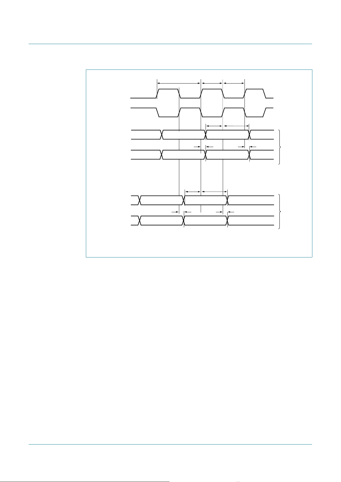
NXP Semiconductors
SCK (CPOL = 0)
MOSI
MISO
T
cy(clk)
t
clk(H)
t
clk(L)
t
DS
t
DH
t
v(Q)
DATA VALID DA TA VALID
t
h(Q)
SCK (CPOL = 1)
DATA VALID
DATA VALID
MOSI
MISO
t
DS
t
DH
t
v(Q)
DATA VALID DA TA VALID
t
h(Q)
DATA VALID
DATA VALID
CPHA = 1
CPHA = 0
002aae830
LPC1311/13/42/43
32-bit ARM Cortex-M3 microcontroller
Fig 30. SSP slave timing in SPI mode
LPC1311_13_42_43 All information provided in this document is subject to legal disclaimers. © NXP B.V. 2012. All rights reserved.
Product data sheet Rev. 5 — 6 June 2012 57 of 74
Page 58

NXP Semiconductors
002aab561
T
PERIOD
differential
data lines
crossover point
source EOP width: t
FEOPT
receiver EOP width: t
EOPR1
, t
EOPR2
crossover point
extended
differential data to
SE0/EOP skew
n × T
PERIOD
+ t
FDEOP
LPC1311/13/42/43
32-bit ARM Cortex-M3 microcontroller
10.8 USB interface (LPC1342/43 only)
Table 20. Dynamic characteristics: USB pins (full-speed)
CL = 50 pF; Rpu = 1.5 kΩ on D+ to VDD, unless otherwise specified. 3.0 V ≤ VDD ≤ 3.6 V
Symbol Parameter Conditions Min Typ Max Unit
t
r
t
f
t
FRFM
V
CRS
t
FEOPT
t
FDEOP
t
JR1
t
JR2
t
EOPR1
t
EOPR2
rise time 10 % to 90 % 8.5 - 13.8 ns
fall time 10 % to 90 % 7.7 - 13.7 ns
differential rise and fall time
tr/t
f
--109%
matching
output signal crossover voltage 1.3 - 2.0 V
source SE0 interval of EOP see Figure 31 160 - 175 ns
source jitter for differential transition
see Figure 31 −2-+5ns
to SE0 transition
receiver jitter to next transition −18.5 - +18.5 ns
receiver jitter for paired transitions 10 % to 90 % −9-+9ns
EOP width at receiver must reject as
[1]
40 - - ns
EOP; see
Figure 31
EOP width at receiver must accept as
[1]
82 - - ns
EOP; see
Figure 31
[1] Characterized but not implemented as production test. Guaranteed by design.
Fig 31. Differential data-to-EOP transition skew and EOP width
LPC1311_13_42_43 All information provided in this document is subject to legal disclaimers. © NXP B.V. 2012. All rights reserved.
Product data sheet Rev. 5 — 6 June 2012 58 of 74
Page 59

NXP Semiconductors
LPC134x
USB-B
connector
USB_DP
USB_CONNECT
soft-connect switch
USB_DM
USB_VBUS
V
SS
V
DD
R1
1.5 kΩ
RS = 33 Ω
002aae608
RS = 33 Ω
LPC134x
V
DD
R1
1.5 kΩ
002aae609
USB-B
connector
USB_DP
USB_DM
USB_VBUS
V
SS
RS = 33 Ω
RS = 33 Ω
11. Application information
11.1 Suggested USB interface solutions (LPC1342/43 only)
LPC1311/13/42/43
32-bit ARM Cortex-M3 microcontroller
Fig 32. LPC1342/43 USB interface on a self-powered device
Fig 33. LPC1342/43 USB interface on a bus-powered device
11.2 XTAL input
LPC1311_13_42_43 All information provided in this document is subject to legal disclaimers. © NXP B.V. 2012. All rights reserved.
Product data sheet Rev. 5 — 6 June 2012 59 of 74
The input voltage to the on-chip oscillators is limited to 1.8 V . If the oscillator is driven by a
clock in slave mode, it is recommended that the input be coupled th rough a cap acitor with
C
= 100 pF. To limit the input voltage to the specified range, choose an additional
i
capacitor to ground C
mode, a minimum of 200 mV(RMS) is needed.
which attenuates the input voltage by a factor Ci/(Ci + Cg). In slave
g
Page 60
NXP Semiconductors
LPC1xxx
XTALIN
C
i
100 pF
C
g
002aae788
002aaf424
LPC1xxx
XTALIN XTALOUT
C
X2
C
X1
XTAL
=
C
L
C
P
R
S
L
Fig 34. Slave mode operation of the on-chip oscillator
In slave mode the input clock signal should be coupled by means of a capacitor of 100 pF
(Figure 34
corresponds to a square wave signal with a signal swing of between 280 mV and 1.4 V.
The XTALOUT pin in this configuration can be left unconnected.
LPC1311/13/42/43
32-bit ARM Cortex-M3 microcontroller
), with an amplitude between 200 mV(RMS) and 1000 mV(RMS). This
External components and models used in oscillation mode are shown in Figure 35
Table 21
and the capacitances C
and Table 22. Since the feedback resistance is integrated on chip, only a crystal
and CX2 need to be connected externally in case of
X1
fundamental mode oscillation (the fundamental frequency is represented by L, C
R
). Capacitance CP in Figure 35 represents the parallel package capacit ance and should
S
not be larger than 7 pF. Parameters F
, CL, RS and CP are supplied by the crystal
OSC
and in
and
L
manufacturer.
Fig 35. Oscillator modes and models: oscillation mode of operation and external crystal
model used for C
X1/CX2
evaluation
LPC1311_13_42_43 All information provided in this document is subject to legal disclaimers. © NXP B.V. 2012. All rights reserved.
Product data sheet Rev. 5 — 6 June 2012 60 of 74
Page 61

NXP Semiconductors
T able 21. Recommended values for CX1/CX2 in oscillation mode (crystal and external
Fundamental oscillation
frequency F
1 MHz - 5 MHz 10 pF < 300 Ω 18 pF, 18 pF
5 MHz - 10 MHz 10 pF < 300 Ω 18 pF, 18 pF
10 MHz - 15 MHz 10 pF < 160 Ω 18 pF, 18 pF
15 MHz - 20 MHz 10 pF < 80 Ω 18 pF, 18 pF
LPC1311/13/42/43
32-bit ARM Cortex-M3 microcontroller
components parameters) low frequency mode
OSC
Crystal load
capacitance C
20 pF < 300 Ω 39 pF, 39 pF
30 pF < 300 Ω 57 pF, 57 pF
20 pF < 200 Ω 39 pF, 39 pF
30 pF < 100 Ω 57 pF, 57 pF
20 pF < 60 Ω 39 pF, 39 pF
Maximum crystal
series resistance R
L
External load
capacitors CX1, C
S
X2
T able 22. Recommended values for C
in oscillation mode (crystal and external
X1/CX2
components parameters) high frequency mode
Fundamental oscillation
frequency F
OSC
Crystal load
capacitance C
Maximum crystal
series resistance R
L
S
15 MHz - 20 MHz 10 pF < 180 Ω 18 pF, 18 pF
20 pF < 100 Ω 39 pF, 39 pF
20 MHz - 25 MHz 10 pF < 160 Ω 18 pF, 18 pF
20 pF < 80 Ω 39 pF, 39 pF
11.3 XTAL Printed-Circuit Board (PCB) layout guidelines
The crystal should be connected on the PCB as close as possible to the oscillator input
and output pins of the chip. Take care that the load capacitors C
third overtone crystal usage have a common ground plane. The external components
must also be connected to the ground plain. Loops must be made as small as possible in
order to keep the noise coupled in via the PCB as small as possible . Also parasitic s
should stay as small as possible. Values of C
and Cx2 should be chosen smaller
x1
accordingly to the increase in parasitics of the PCB layout.
x1
External load
capacitors CX1, C
X2
, Cx2, and Cx3 in case of
LPC1311_13_42_43 All information provided in this document is subject to legal disclaimers. © NXP B.V. 2012. All rights reserved.
Product data sheet Rev. 5 — 6 June 2012 61 of 74
Page 62
NXP Semiconductors
PIN
V
DD
ESD
V
SS
ESD
V
DD
weak
pull-up
weak
pull-down
output enable
repeater mode
enable
output
pull-up enable
pull-down enable
data input
analog input
select analog input
002aaf304
pin configured
as digital output
driver
pin configured
as digital input
pin configured
as analog input
11.4 Standard I/O pad configuration
Figure 36 shows the possible pin modes for standard I/O pins with analog input function:
• Digital output driver
• Digital input: Pull-up enabled/disabled
• Digital input: Pull-down enabled/disabled
• Digital input: Repeater mode enabled/disabled
• Analog input
LPC1311/13/42/43
32-bit ARM Cortex-M3 microcontroller
Fig 36. Standard I/O pad configuration
LPC1311_13_42_43 All information provided in this document is subject to legal disclaimers. © NXP B.V. 2012. All rights reserved.
Product data sheet Rev. 5 — 6 June 2012 62 of 74
Page 63

NXP Semiconductors
V
SS
reset
002aaf274
V
DD
V
DD
V
DD
R
pu
ESD
ESD
20 ns RC
GLITCH FILTER
PIN
11.5 Reset pad configuration
Fig 37. Reset pad configuration
LPC1311/13/42/43
32-bit ARM Cortex-M3 microcontroller
11.6 ADC usage notes
The following guidelines show how to increase the performance of the ADC in a noisy
environment beyond the ADC specifications listed in Table 8
• The ADC input trace must be short and as close as possible to the LPC1311/13/42/43
chip.
• The ADC input traces must be shielded from fast switching digital signals and noisy
power supply lines.
• Because the ADC and the digital core share the same power supply, the power supply
line must be adequately filtered.
• To improve the ADC performance in a very noisy environment, put the device in Sleep
mode during the ADC conversion.
:
LPC1311_13_42_43 All information provided in this document is subject to legal disclaimers. © NXP B.V. 2012. All rights reserved.
Product data sheet Rev. 5 — 6 June 2012 63 of 74
Page 64

NXP Semiconductors
1 1.7 ElectroMagnetic Compatibility (EMC)
Radiated emission measurements according to the IEC61967-2 standard using the
TEM-cell method are shown for the LPC1343FBD48 in Table 23
Table 23. ElectroMagnetic Compatibility (EMC) for part LPC1343FBD48 (TEM-cell method)
VDD = 3.3 V; T
Parameter Frequency band System clock = Unit
Input clock: IRC (12 MHz)
maximum
peak level
IEC level
Input clock: crystal oscillator (12 MHz)
maximum
peak level
IEC level
LPC1311/13/42/43
32-bit ARM Cortex-M3 microcontroller
.
= 25 °C.
amb
12 MHz 24 MHz 48 MHz 72 MHz
150 kHz - 30 MHz −6 −5 −7 −7dBμV
30 MHz - 150 MHz −1+3+9+13dBμV
150 MHz - 1 GHz +3 +7 +15 +19 dBμV
[1]
-ONML-
150 kHz - 30 MHz -5 −5 −7 −7dBμV
30 MHz - 150 MHz 0 +4 +9 +13 dBμV
150 MHz - 1 GHz 3 +8 +15 +20 dBμV
[1]
-ONML-
[1] IEC levels refer to Appendix D in the IEC61967-2 Specification.
LPC1311_13_42_43 All information provided in this document is subject to legal disclaimers. © NXP B.V. 2012. All rights reserved.
Product data sheet Rev. 5 — 6 June 2012 64 of 74
Page 65

NXP Semiconductors
UNIT
A
max.
A1A2A3bpcE
(1)
eH
E
LL
p
Zywv θ
REFERENCES
OUTLINE
VERSION
EUROPEAN
PROJECTION
ISSUE DATE
IEC JEDEC JEITA
mm
1.6
0.20
0.05
1.45
1.35
0.25
0.27
0.17
0.18
0.12
7.1
6.9
0.5
9.15
8.85
0.95
0.55
7
0
o
o
0.12 0.10.21
DIMENSIONS (mm are the original dimensions)
Note
1. Plastic or metal protrusions of 0.25 mm maximum per side are not included.
0.75
0.45
SOT313-2 MS-026136E05
00-01-19
03-02-25
D
(1) (1)(1)
7.1
6.9
H
D
9.15
8.85
E
Z
0.95
0.55
D
b
p
e
E
B
12
D
H
b
p
E
H
v M
B
D
Z
D
A
Z
E
e
v M
A
1
48
37
36
25
24
13
θ
A
1
A
L
p
detail X
L
(A )
3
A
2
X
y
c
w M
w M
0 2.5 5 mm
scale
pin 1 index
LQFP48: plastic low profile quad flat package; 48 leads; body 7 x 7 x 1.4 mm
SOT313-2
12. Package outline
LPC1311/13/42/43
32-bit ARM Cortex-M3 microcontroller
Fig 38. Package outline SOT313-2 (LQFP48)
LPC1311_13_42_43 All information provided in this document is subject to legal disclaimers. © NXP B.V. 2012. All rights reserved.
Product data sheet Rev. 5 — 6 June 2012 65 of 74
Page 66

NXP Semiconductors
References
Outline
version
European
projection
Issue date
IEC JEDEC JEITA
- - -
hvqfn33_po
09-03-17
09-03-23
Unit
mm
max
nom
min
1.00
0.85
0.80
0.05
0.02
0.00
0.2
7.1
7.0
6.9
4.85
4.70
4.55
7.1
7.0
6.9
0.65 4.55
0.75
0.60
0.45
0.1
A
(1)
Dimensions
Note
1. Plastic or metal protrusions of 0.075 mm maximum per side are not included.
HVQFN33: plastic thermal enhanced very thin quad flat package; no leads;
33 terminals; body 7 x 7 x 0.85 mm
A1b
0.35
0.28
0.23
cD
(1)
DhE
(1)
E
h
4.85
4.70
4.55
ee
1e2
4.55
Lv
0.1w0.05y0.08
y
1
0 2.5 5 mm
scale
terminal 1
index area
B
A
D
E
C
y
C
y
1
X
detail X
A
1
A
c
b
e
2
e
1
e
e
AC
B
v
Cw
terminal 1
index area
D
h
E
h
L
9 16
32
33
25
17
24
8
1
LPC1311/13/42/43
32-bit ARM Cortex-M3 microcontroller
Fig 39. Package outline (HVQFN33)
LPC1311_13_42_43 All information provided in this document is subject to legal disclaimers. © NXP B.V. 2012. All rights reserved.
Product data sheet Rev. 5 — 6 June 2012 66 of 74
Page 67

NXP Semiconductors
SOT313-2
DIMENSIONS in mm
occupied area
Footprint information for reflow soldering of LQFP48 package
Ax
Bx
Gx
Gy
Hy
Hx
AyBy
P1
D2 (8×)
D1
(0.125)
Ax Ay Bx By D1 D2 Gx Gy Hx Hy
10.350
P2
0.560 10.350 7.350 7.350
P1
0.500 0.280
C
1.500 0.500 7.500 7.500 10.650 10.650
sot313-2_fr
solder land
C
Generic footprint pattern
Refer to the package outline drawing for actual layout
P2
13. Soldering
LPC1311/13/42/43
32-bit ARM Cortex-M3 microcontroller
Fig 40. Reflow soldering of the LQFP48 package
LPC1311_13_42_43 All information provided in this document is subject to legal disclaimers. © NXP B.V. 2012. All rights reserved.
Product data sheet Rev. 5 — 6 June 2012 67 of 74
Page 68
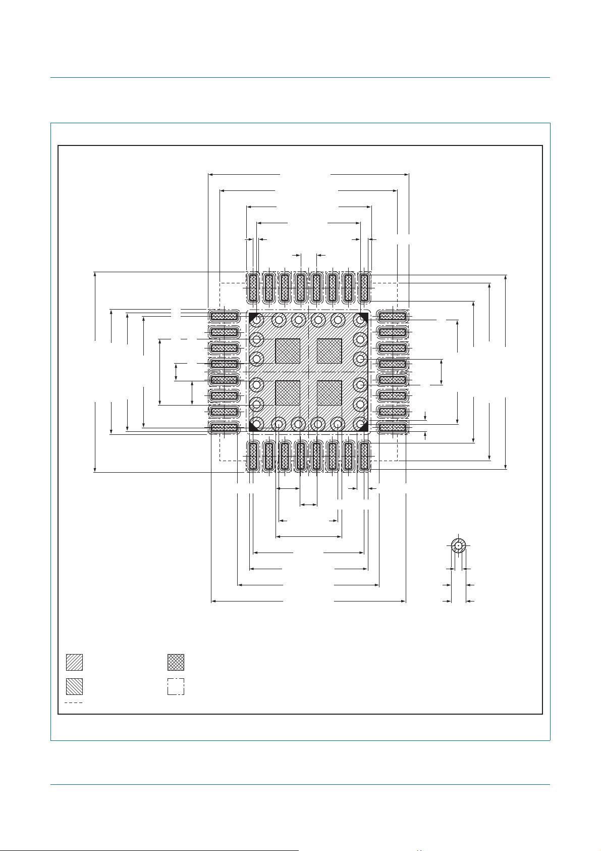
NXP Semiconductors
Footprint information for reflow soldering of HVQFN33 package
PID = 7.25 PA+OA
0.20 SR
chamfer (4×)
LPC1311/13/42/43
32-bit ARM Cortex-M3 microcontroller
OID = 8.20 OA
OwDtot = 5.10 OA
evia = 4.25
W = 0.30 CU
e = 0.65
OIE = 8.20 OA
EHS = 4.85 CU
OwEtot = 5.10 OA
GapE = 0.70 SP
4.55 SR
SEhtot = 2.70 SP
SPE = 1.00 SP
SPD = 1.00 SP
GapD = 0.70 SP
evia = 2.40
SDhtot = 2.70 SP
4.55 SR
DHS = 4.85 CU
LbD = 5.80 CU
LaD = 7.95 CU
0.45 DM
evia = 1.05
evia = 4.25
LbE = 5.80 CU
0.45 DM
B-side
Solder resist
covered via
0.30 PH
0.60 SR cover
0.60 CU
(A-side fully covered)
number of vias: 20
LaE = 7.95 CU
PIE = 7.25 PA+OA
solder land
solder paste deposit
occupied area
solder land plus solder paste
solder resist
Dimensions in mm
Remark:
Stencil thickness: 0.125 mm
001aao134
Fig 41. Reflow soldering of the HVQFN33 package
LPC1311_13_42_43 All information provided in this document is subject to legal disclaimers. © NXP B.V. 2012. All rights reserved.
Product data sheet Rev. 5 — 6 June 2012 68 of 74
Page 69

NXP Semiconductors
14. Abbreviations
Table 24. Abbreviations
Acronym Description
A/D Analog-to-Digital
ADC Analog-to-Digital Converter
AHB Advanced High-performance Bus
AMBA Advanced Microcontrol ler Bus Archite cture
APB Advanced Peripheral Bus
BOD BrownOut Detection
EOP End Of Packet
ETM Embedded Trace Macrocell
FIFO First-In, First-Out
GPIO General Purpose Input/Output
HID Human Interface Device
I/O Input/Output
LSB Least Significant Bit
MSC Mass Storage Class
PHY Physical Layer
PLL Phase-Locked Loop
SE0 Single Ended Zero
SPI Serial Peripheral Interface
SSI Serial Synchronous Interface
SSP Synchronous Serial Port
SoF Start-of-Frame
TCM Tightly-Coupled Memory
TTL Transistor-Transi sto r Lo g ic
UART Universal Asynchronous Receiver/Transmitter
USB Universal Serial Bus
LPC1311/13/42/43
32-bit ARM Cortex-M3 microcontroller
LPC1311_13_42_43 All information provided in this document is subject to legal disclaimers. © NXP B.V. 2012. All rights reserved.
Product data sheet Rev. 5 — 6 June 2012 69 of 74
Page 70

NXP Semiconductors
LPC1311/13/42/43
32-bit ARM Cortex-M3 microcontroller
15. Revision history
Table 25. Revision history
Document ID Release date Data sheet status Change notice Supersedes
LPC1311_13_42_43 v.5 20120606 Product data sheet - LPC1311_13_42_43 v.4
Modifications:
• Parameters V
Table 7.
• Condition “The peak current is limited to 25 times the corresponding maximum
current.” removed from parameters IDD and ISS in Table 6.
LPC1311_13_42_43 v.4 20110620 Product data sheet - LPC1311_13_42_43 v.3
LPC1311_13_42_43 v.3 20100810 Product data sheet - LPC1311_13_42_43 v.2
LPC1311_13_42_43 v.2 20100506 Product data sheet - LPC1311_13_42_43 v.1
LPC1311_13_42_43 v.1 20091211 Product data sheet - -
, VOH, IOL, IOH updated for voltage range 2.0 V ≤ VDD < 2.5 V in
OL
LPC1311_13_42_43 All information provided in this document is subject to legal disclaimers. © NXP B.V. 2012. All rights reserved.
Product data sheet Rev. 5 — 6 June 2012 70 of 74
Page 71

NXP Semiconductors
LPC1311/13/42/43
32-bit ARM Cortex-M3 microcontroller
16. Legal information
16.1 Data sheet status
Document status
Objective [short] data sheet Development This document contains data from the objective specification for product development.
Preliminary [short] data sheet Qualification This document contains data from the preliminary specification.
Product [short] data sheet Production This document contains the product specification.
[1] Please consult the most recently issued document before initiating or completing a design.
[2] The term ‘short data sheet’ is explained in section “Definitions”.
[3] The product status of device(s) described in this document may have changed since thi s docume nt was publish ed and ma y dif fer in case of multiple devices. The latest product status
information is available on the Internet at URL http://www.nxp.com.
[1][2]
Product status
[3]
Definition
16.2 Definitions
Draft — The document is a draft version only. The content is still under
internal review and subject to formal approval, which may result in
modifications or additions. NXP Semiconductors does not give any
representations or warranties as to the accuracy or completeness of
information included herein and shall have no liability for the consequences of
use of such information.
Short data sheet — A short data sheet is an extract from a full data sheet
with the same product type number(s) and title. A short data sheet is intended
for quick reference only and should not be relied upon to co nt ain det ailed and
full information. For detailed and full information see the relevant full data
sheet, which is available on request via the local NXP Semiconductors sales
office. In case of any inconsistency or conflict with the short data sheet, the
full data sheet shall prevail.
Product specification — The information and data provided in a Product
data sheet shall define the specification of the product as agreed between
NXP Semiconductors and its customer, unless NXP Semiconductors and
customer have explicitly agreed otherwise in writing. In no event however,
shall an agreement be valid in which the NXP Semiconductors product is
deemed to offer functions and qualities beyond those described in the
Product data sheet.
16.3 Disclaimers
Limited warranty and liability — Information in this document is believed to
be accurate and reliable. However, NXP Semiconductors does not give any
representations or warranties, expressed or implied, as to the accuracy or
completeness of such information and shall have no liability for the
consequences of use of such information. NXP Semiconductors takes no
responsibility for the content in this document if provided by an information
source outside of NXP Semiconductors.
In no event shall NXP Semiconductors be liable for any indirect, incidental,
punitive, special or consequential damages (including - without limitation - lost
profits, lost savings, business interruption, costs related to the removal or
replacement of any products or rework charges) whether or not such
damages are based on tort (including negligence), warranty, breach of
contract or any other legal theory.
Notwithstanding any damages that customer might incur for any reason
whatsoever, NXP Semi conductors’ aggregat e and cumulative liabil ity towards
customer for the products described herein shall be limited in accordance
with the Terms and conditions of commercial sale of NXP Semiconductors.
Right to make changes — NXP Semiconductors reserves the right to make
changes to information published in this document, including without
limitation specifications and product descriptions, at any time and without
notice. This document supersedes and replaces all information supplied prior
to the publication hereof.
LPC1311_13_42_43 All information provided in this document is subject to legal disclaimers. © NXP B.V. 2012. All rights reserved.
Suitability for use — NXP Semiconductors products are not designed,
authorized or warranted to be suitable for use in life support, life-critical or
safety-critical systems or equipment, nor in applications where failure or
malfunction of an NXP Semiconductors product can reasonably be expected
to result in personal injury, death or severe property or environmental
damage. NXP Semiconductors and its suppliers accept no liability for
inclusion and/or use of NXP Semiconductors products in such equipment or
applications and therefore such inclusion and/or use is at the cust omer’s own
risk.
Applications — Applications that are described herein for any of these
products are for illustrative purposes only. NXP Semiconductors makes no
representation or warranty that such applications will be suitable for the
specified use without further testing or modification.
Customers are responsible for the design and operation of their applications
and products using NXP Semiconductors products, and NXP Semiconductors
accepts no liability for any assistance with applications or cust omer product
design. It is customer’s sole responsibility to determine whether the NXP
Semiconductors product is suitable and fit for the customer’s applications and
products planned, as well as for the planned application and use of
customer’s third party customer(s). Customers should provide appropriate
design and operating safeguards to minimize the risks associated with their
applications and products.
NXP Semiconductors does not accept any liability related to any default ,
damage, costs or problem which is based on any weakness or default in the
customer’s applications or products, or the application or use by customer’s
third party customer(s). Customer is responsible for doing all necessary
testing for the customer’s applications and products using NXP
Semiconductors products in order to avoid a default of the applications and
the products or of the application or use by customer’s third part y
customer(s). NXP does not accept any liability in this respect.
Limiting values — Stress above one or more limiting values (as defined in
the Absolute Maximum Ratings System of IEC 60134) will cause permanent
damage to the device. Limiting values are stress ratings only and (proper)
operation of the device at these or any other conditions above those given in
the Recommended operating conditions section (if present) or the
Characteristics sections of this document is not warranted. Constant or
repeated exposure to limiting values will permanently and irreversibly affect
the quality and reliability of the device.
Terms and conditions of commercial sale — NXP Semiconductors
products are sold subject to the general terms and conditions of commercial
sale, as published at http://www.nxp.com/profile/terms
agreed in a valid written individual agreement. In case an individual
agreement is concluded only the terms and conditions of the respective
agreement shall apply. NXP Semiconductors hereby expressly objects to
applying the customer’s general terms and conditions with regard to the
purchase of NXP Semiconductors products by customer.
No offer to sell or license — Nothing in this document may be interpreted or
construed as an offer to sell product s that is open for accept ance or the gr ant,
conveyance or implication of any license under any copyrights, patents or
other industrial or intellectual property rights.
, unless otherwise
Product data sheet Rev. 5 — 6 June 2012 71 of 74
Page 72

NXP Semiconductors
LPC1311/13/42/43
32-bit ARM Cortex-M3 microcontroller
Export control — This document as well as the item(s) described herein
may be subject to export control regulations. Export might require a prior
authorization from competent authorities.
Non-automotive qualified products — Unless this data sheet expressly
states that this specific NXP Semiconductors product is automotive qualified,
the product is not suitable for automotive use. It i s neit her qua lif ied nor tested
in accordance with automotive testing or application requirements. NXP
Semiconductors accepts no liability for inclusion and/or use of
non-automotive qualified products in automotive equipment or applications.
In the event that customer uses the product for design-in and use in
automotive applications to automotive specifications and standards, custome r
(a) shall use the product without NXP Semiconductors’ warranty of the
product for such automotive applications, use and specifications, and (b)
whenever customer uses the product for automotive applications beyond
NXP Semiconductors’ specifications such use shall be solely at customer’s
own risk, and (c) customer fully indemnifies NXP Semiconductors for any
liability, da mages or failed produ ct claims result ing from custome r design and
use of the product for automotive applications beyond NXP Semiconductors’
standard warranty and NXP Semiconductors’ product specifications.
16.4 Trademarks
Notice: All referenced brands, product names, service names and trademarks
are the property of their respective owners.
2
I
C-bus — logo is a trademark of NXP B.V.
17. Contact information
For more information, please visit: http://www.nxp.com
For sales office addresses, please send an email to: salesaddresses@nxp.com
LPC1311_13_42_43 All information provided in this document is subject to legal disclaimers. © NXP B.V. 2012. All rights reserved.
Product data sheet Rev. 5 — 6 June 2012 72 of 74
Page 73

NXP Semiconductors
18. Contents
LPC1311/13/42/43
32-bit ARM Cortex-M3 microcontroller
1 General description . . . . . . . . . . . . . . . . . . . . . . 1
2 Features and benefits . . . . . . . . . . . . . . . . . . . . 1
3 Applications . . . . . . . . . . . . . . . . . . . . . . . . . . . . 3
4 Ordering information. . . . . . . . . . . . . . . . . . . . . 3
4.1 Ordering options. . . . . . . . . . . . . . . . . . . . . . . . 3
5 Block diagram . . . . . . . . . . . . . . . . . . . . . . . . . . 5
6 Pinning information. . . . . . . . . . . . . . . . . . . . . . 6
6.1 Pinning . . . . . . . . . . . . . . . . . . . . . . . . . . . . . . . 6
6.2 Pin description . . . . . . . . . . . . . . . . . . . . . . . . 10
7 Functional description . . . . . . . . . . . . . . . . . . 17
7.1 Architectural overview . . . . . . . . . . . . . . . . . . 17
7.2 ARM Cortex-M3 processor. . . . . . . . . . . . . . . 17
7.3 On-chip flash program memory . . . . . . . . . . . 17
7.4 On-chip SRAM . . . . . . . . . . . . . . . . . . . . . . . . 17
7.5 Memory map . . . . . . . . . . . . . . . . . . . . . . . . . . 17
7.6 Nested Vectored Interrupt Controller (NVIC) . 18
7.6.1 Features . . . . . . . . . . . . . . . . . . . . . . . . . . . . . 19
7.6.2 Interrupt sources. . . . . . . . . . . . . . . . . . . . . . . 19
7.7 IOCONFIG block . . . . . . . . . . . . . . . . . . . . . . 19
7.8 Fast general purpose parallel I/O . . . . . . . . . . 19
7.8.1 Features . . . . . . . . . . . . . . . . . . . . . . . . . . . . . 19
7.9 USB interface (LPC1342/43 only) . . . . . . . . . 20
7.9.1 Full-speed USB device controller . . . . . . . . . . 20
7.9.1.1 Features . . . . . . . . . . . . . . . . . . . . . . . . . . . . . 20
7.10 UART . . . . . . . . . . . . . . . . . . . . . . . . . . . . . . . 21
7.10.1 Features . . . . . . . . . . . . . . . . . . . . . . . . . . . . . 21
7.11 SSP serial I/O controller . . . . . . . . . . . . . . . . . 21
7.11.1 Features . . . . . . . . . . . . . . . . . . . . . . . . . . . . . 21
7.12 I
7.12.1 Features . . . . . . . . . . . . . . . . . . . . . . . . . . . . . 22
7.13 10-bit ADC . . . . . . . . . . . . . . . . . . . . . . . . . . . 22
7.13.1 Features . . . . . . . . . . . . . . . . . . . . . . . . . . . . . 22
7.14 General purpose external event
7.14.1 Features . . . . . . . . . . . . . . . . . . . . . . . . . . . . . 23
7.15 System tick timer . . . . . . . . . . . . . . . . . . . . . . 23
7.16 Watchdog timer. . . . . . . . . . . . . . . . . . . . . . . . 23
7.16.1 Features . . . . . . . . . . . . . . . . . . . . . . . . . . . . . 23
7.17 Windowed WatchDog Timer (WWDT) . . . . . . 24
7.17.1 Features . . . . . . . . . . . . . . . . . . . . . . . . . . . . . 24
7.18 Clocking and power control . . . . . . . . . . . . . . 24
7.18.1 Integrated oscillators . . . . . . . . . . . . . . . . . . . 24
7.18.1.1 Internal RC oscillator . . . . . . . . . . . . . . . . . . . 25
7.18.1.2 System oscillator . . . . . . . . . . . . . . . . . . . . . . 26
7.18.1.3 Watchdog oscillator . . . . . . . . . . . . . . . . . . . . 26
7.18.2 System PLL and USB PLL . . . . . . . . . . . . . . . 26
7.18.3 Clock output . . . . . . . . . . . . . . . . . . . . . . . . . . 26
2
C-bus serial I/O controller . . . . . . . . . . . . . . 21
counter/timers. . . . . . . . . . . . . . . . . . . . . . . . . 23
7.18.4 Wake-up process. . . . . . . . . . . . . . . . . . . . . . 26
7.18.5 Power control. . . . . . . . . . . . . . . . . . . . . . . . . 27
7.18.5.1 Power profiles (LPC1300L series,
LPC1311/01 and LPC1313/01 only) . . . . . . . 27
7.18.5.2 Sleep mode . . . . . . . . . . . . . . . . . . . . . . . . . . 27
7.18.5.3 Deep-sleep mode. . . . . . . . . . . . . . . . . . . . . . 27
7.18.5.4 Deep power-down mode . . . . . . . . . . . . . . . . 28
7.19 System control . . . . . . . . . . . . . . . . . . . . . . . . 28
7.19.1 Start logic. . . . . . . . . . . . . . . . . . . . . . . . . . . . 28
7.19.2 Reset . . . . . . . . . . . . . . . . . . . . . . . . . . . . . . . 28
7.19.3 Brownout detection . . . . . . . . . . . . . . . . . . . . 28
7.19.4 Code security (Code Read Protection - CRP) 28
7.19.5 Boot loader. . . . . . . . . . . . . . . . . . . . . . . . . . . 29
7.19.6 APB interface. . . . . . . . . . . . . . . . . . . . . . . . . 29
7.19.7 AHB-Lite . . . . . . . . . . . . . . . . . . . . . . . . . . . . 29
7.19.8 External interrupt inputs. . . . . . . . . . . . . . . . . 29
7.19.9 Memory mapping control . . . . . . . . . . . . . . . . 29
7.20 Emulation and debugging . . . . . . . . . . . . . . . 30
8 Limiting values . . . . . . . . . . . . . . . . . . . . . . . . 31
9 Static characteristics . . . . . . . . . . . . . . . . . . . 32
9.1 BOD static characteristics for LPC1300 series 38
9.2 BOD static characteristics for LPC1300L series
(LPC1311/01 and LPC1313/01). . . . . . . . . . . 39
9.3 Power consumption for LPC1300 series . . . . 39
9.4 Power consumption for LPC1300L series
(LPC1311/01 and LPC1313/01). . . . . . . . . . . 42
9.5 Peripheral power consumption . . . . . . . . . . . 45
9.6 Electrical pin characteristics. . . . . . . . . . . . . . 46
10 Dynamic characteristics. . . . . . . . . . . . . . . . . 50
10.1 Power-up ramp conditions . . . . . . . . . . . . . . . 50
10.2 Flash memory . . . . . . . . . . . . . . . . . . . . . . . . 50
10.3 External clock. . . . . . . . . . . . . . . . . . . . . . . . . 51
10.4 Internal oscillators . . . . . . . . . . . . . . . . . . . . . 52
10.5 I/O pins . . . . . . . . . . . . . . . . . . . . . . . . . . . . . 53
10.6 I
10.7 SSP0/1 interface . . . . . . . . . . . . . . . . . . . . . . 55
10.8 USB interface (LPC1342/43 only) . . . . . . . . . 58
11 Application information . . . . . . . . . . . . . . . . . 59
11.1 Suggested USB interface solutions
11.2 XTAL input . . . . . . . . . . . . . . . . . . . . . . . . . . . 59
11.3 XTAL Printed-Circuit Board (PCB) layout
11.4 Standard I/O pad configuration . . . . . . . . . . . 62
11.5 Reset pad configuration. . . . . . . . . . . . . . . . . 63
11.6 ADC usage notes. . . . . . . . . . . . . . . . . . . . . . 63
11.7 ElectroMagnetic Compatibility (EMC) . . . . . . 64
2
C-bus. . . . . . . . . . . . . . . . . . . . . . . . . . . . . . 53
(LPC1342/43 only). . . . . . . . . . . . . . . . . . . . . 59
guidelines. . . . . . . . . . . . . . . . . . . . . . . . . . . . 61
continued >>
LPC1311_13_42_43 All information provided in this document is subject to legal disclaimers. © NXP B.V. 2012. All rights reserved.
Product data sheet Rev. 5 — 6 June 2012 73 of 74
Page 74

NXP Semiconductors
12 Package outline . . . . . . . . . . . . . . . . . . . . . . . . 65
13 Soldering . . . . . . . . . . . . . . . . . . . . . . . . . . . . . 67
14 Abbreviations . . . . . . . . . . . . . . . . . . . . . . . . . . 69
15 Revision history. . . . . . . . . . . . . . . . . . . . . . . . 70
16 Legal information. . . . . . . . . . . . . . . . . . . . . . . 71
16.1 Data sheet status . . . . . . . . . . . . . . . . . . . . . . 71
16.2 Definitions. . . . . . . . . . . . . . . . . . . . . . . . . . . . 71
16.3 Disclaimers. . . . . . . . . . . . . . . . . . . . . . . . . . . 71
16.4 Trademarks. . . . . . . . . . . . . . . . . . . . . . . . . . . 72
17 Contact information. . . . . . . . . . . . . . . . . . . . . 72
18 Contents. . . . . . . . . . . . . . . . . . . . . . . . . . . . . . 73
LPC1311/13/42/43
32-bit ARM Cortex-M3 microcontroller
Please be aware that important notices concerning this document and the product(s)
described herein, have been included in section ‘Legal information’.
© NXP B.V. 2012. All rights reserved.
For more information, please visit: http://www.nxp.com
For sales office addresses, please send an email to: salesaddresses@nxp.com
Document identifier: LPC1311_13_42_43
Date of release: 6 June 2012
 Loading...