

Page 1
UM11374
KITPF5023FRDMEVM evaluation board
Rev. 1 — 30 June 2020 User manual
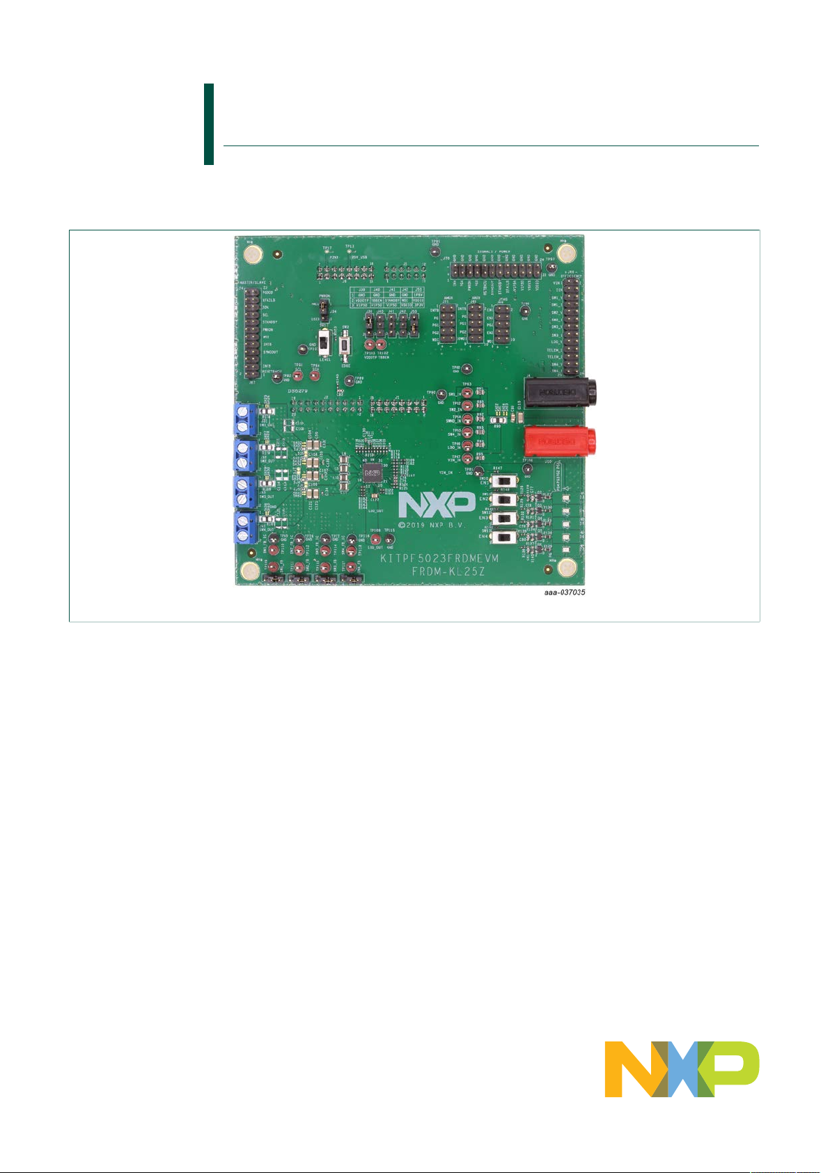
Figure 1. KITPF5023FRDMEVM
Page 2

NXP Semiconductors
UM11374
KITPF5023FRDMEVM evaluation board
Important Notice
NXP provides the enclosed product(s) under the following conditions:
This evaluation kit is intended for use of ENGINEERING DEVELOPMENT OR EVALUATION PURPOSES ONLY. It is provided as a
sample IC pre-soldered to a printed circuit board to make it easier to access inputs, outputs, and supply terminals. This evaluation board
may be used with any development system or other source of I/O signals by simply connecting it to the host MCU or computer board via
off-the-shelf cables. This evaluation board is not a Reference Design and is not intended to represent a final design recommendation for
any particular application. Final device in an application will be heavily dependent on proper printed circuit board layout and heat sinking
design as well as attention to supply filtering, transient suppression, and I/O signal quality.
The goods provided may not be complete in terms of required design, marketing, and or manufacturing related protective considerations,
including product safety measures typically found in the end product incorporating the goods. Due to the open construction of the product,
it is the user's responsibility to take any and all appropriate precautions with regard to electrostatic discharge. In order to minimize risks
associated with the customers applications, adequate design and operating safeguards must be provided by the customer to minimize
inherent or procedural hazards. For any safety concerns, contact NXP sales and technical support services.
Should this evaluation kit not meet the specifications indicated in the kit, it may be returned within 30 days from the date of delivery and will
be replaced by a new kit.
NXP reserves the right to make changes without further notice to any products herein. NXP makes no warranty, representation or
guarantee regarding the suitability of its products for any particular purpose, nor does NXP assume any liability arising out of the
application or use of any product or circuit, and specifically disclaims any and all liability, including without limitation consequential or
incidental damages. Typical parameters can and do vary in different applications and actual performance may vary over time. All operating
parameters, including Typical, must be validated for each customer application by customer’s technical experts.
NXP does not convey any license under its patent rights nor the rights of others. NXP products are not designed, intended, or authorized
for use as components in systems intended for surgical implant into the body, or other applications intended to support or sustain life, or
for any other application in which the failure of the NXP product could create a situation where personal injury or death may occur.
Should the Buyer purchase or use NXP products for any such unintended or unauthorized application, the Buyer shall indemnify and hold
NXP and its officers, employees, subsidiaries, affiliates, and distributors harmless against all claims, costs, damages, and expenses, and
reasonable attorney fees arising out of, directly or indirectly, any claim of personal injury or death associated with such unintended or
unauthorized use, even if such claim alleges NXP was negligent regarding the design or manufacture of the part.
UM11374 All information provided in this document is subject to legal disclaimers. © NXP B.V. 2020. All rights reserved.
User manual Rev. 1 — 30 June 2020
2 / 26
Page 3

NXP Semiconductors
KITPF5023FRDMEVM evaluation board
1 Introduction
This document is the user guide for the KITPF5023FRDMEVM evaluation board.
This document is intended for the engineers involved in the evaluation, design,
implementation, and validation of PF5023 Power management integrated circuit (PMIC)
for high performance applications.
The scope of this document is to provide the user with information that covers interfacing
with the hardware, installing the GUI software, using other tools, and configuring the
board for the application environment.
2 Finding kit resources and information on the NXP web site
NXP Semiconductors provides online resources for this evaluation board and its
supported device(s) on http://www.nxp.com.
The information page for KITPF5023FRDMEVM evaluation board is at http://
www.nxp.com/KITPF5023FRDMEVM. The information page provides overview
information, documentation, software and tools, parametrics, ordering information
and a Getting Started tab. The Getting Started tab provides quick-reference
information applicable to using the KITPF5023FRDMEVM evaluation board, including the
downloadable assets referenced in this document.
UM11374
2.1 Collaborate in the NXP community
The NXP community is for sharing ideas and tips, ask and answer technical questions,
and receive input on just about any embedded design topic.
The NXP community is at http://community.nxp.com.
3 Getting ready
Working with the KITPF5023FRDMEVM requires the kit contents, additional hardware
and a Windows PC workstation with installed software.
3.1 Kit contents
• Assembled and tested KITPF5023FRDMEVM connected to FRDM-KL25Z in an anti-
• 3.0 ft USB-STD A to USB-B-mini cable
3.2 Additional hardware
In addition to the kit contents, the following hardware is necessary or beneficial when
working with this kit.
• Power supply with a range of 2.5 V to 6.0 V and current limit set initially to 100 mA
static bag
3.3 Windows PC workstation
This evaluation board requires a Windows PC workstation. Meeting these minimum
specifications should produce great results when working with this evaluation board.
• USB-enabled computer with Windows 7 or Windows 10
UM11374 All information provided in this document is subject to legal disclaimers. © NXP B.V. 2020. All rights reserved.
User manual Rev. 1 — 30 June 2020
3 / 26
Page 4

NXP Semiconductors
3.4 Software
Installing software is necessary to work with this evaluation board. All listed software
is available on the evaluation board's information page at http://www.nxp.com/
KITPF5023FRDMEVM.
• NXP_GUI_ PR_1.0: software interface GUI, tool to configure OTP, generate TBB and
OTP scripts
4 Getting to know the hardware
The KITPF5023FRDMEVM evaluation board is the complete evaluation kit of the
PF5023 power management IC from NXP Semiconductors. This user guide describes
the functionality of the evaluation board, explains how to use the PMIC device in an
application environment, and gives details about the hardware and software required.
The KITPF5023FRDMEVM board is the dedicated kit for the PF5023 PMIC but it is also
compatible with other PMIC devices in the family like the PF5020 and PF5024.
4.1 KITPF5023FRDMEVM features
UM11374
KITPF5023FRDMEVM evaluation board
• SW1, SW2, SW3 in single-phase mode (default) or multiphase mode up to 3.5 A peak
each
• PWRON switch for global wake up or enable
• Individual enable control switch for each regulator
• LEDs to indicate individual PGOODx and global PGOOD status
• USB interface through FRDM-KL25Z for register access, TBB mode, and OTP
programming
• Multiple signal connectors for easy access
• Terminal blocks and test point for all the regulators for easy testing and evaluation
UM11374 All information provided in this document is subject to legal disclaimers. © NXP B.V. 2020. All rights reserved.
User manual Rev. 1 — 30 June 2020
4 / 26
Page 5
NXP Semiconductors
4.2 Kit featured components
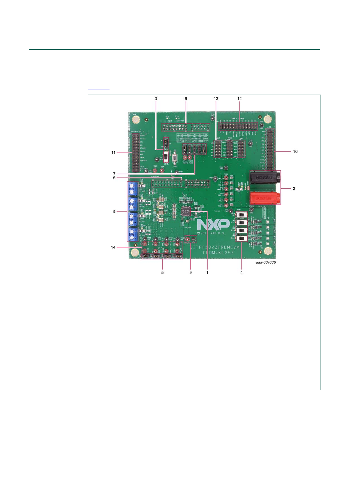
Figure 2 identifies important components on the board.
UM11374
KITPF5023FRDMEVM evaluation board
1. PF5023 PMIC
2. VIN connector
3. PWRON control switch and jumper
4. Enable switches for the regulators
5. Feedback jumpers for the buck regulators
6. FRDM-KL25Z connectors (for SW/GUI interface) – on the bottom side of the board
7. Jumpers for IO control (TBBEN, VDDOTP, STANDBY, WDI, VDDIO)
8. Load terminal for the buck outputs
9. Load / test point for LDO1 output
10. Connector for efficiency measurement
11. Connector for master/slave (multi-PMIC) connection
12. Connector for signals and power measurement
13. Connectors for IO measurement
14. Feedback test points of buck regulators to measure loop stability
Figure 2. Evaluation board featured component locations
4.2.1 PF5023: Power management integrated circuit (PMIC) for high performance applications
4.2.1.1 General description
The PF5023 integrates multiple high performance buck regulators. It can operate as a
stand-alone point-of-load regulator IC, or as a companion chip to a larger PMIC.
UM11374 All information provided in this document is subject to legal disclaimers. © NXP B.V. 2020. All rights reserved.
User manual Rev. 1 — 30 June 2020
5 / 26
Page 6

NXP Semiconductors
UM11374
KITPF5023FRDMEVM evaluation board
Built-in one-time programmable (OTP) memory stores key startup configurations,
drastically reducing external components typically used to set output voltage and
sequence of regulators. Regulator parameters are adjustable through high-speed I2C
after start up offering flexibility for different system states.
4.2.1.2 Features
• Three high efficiency buck converters
• VTT Termination mode on SW2
• Watchdog timer/monitor
• Monitoring circuit to fit ASIL B safety level
• One-time programmable device configuration
• 3.4 MHz I2C communication interface
• 40-pin QFN package with wettable flank and exposed pad
4.2.2 Jumper, switch, and shunt configuration
Table 1. Evaluation board jumper, switch, and shunt descriptions
Jumper/switch Default Description
J1, J2, J5, J6 — Freedom KL25Z board interface connectors
J34 Open Control PWRON pull up source
2-3 → PWRON pulled up to VIN
Open → full MCU control with no pull up
J39 1-2 shorted Select PF5023 default register configuration
1-2 → OTP mode
2-3 → Hardwire mode
J40 Open Enable TBB mode on PF5023 device
1-2 → TBB mode disabled
2-3 → TBB mode enabled
Open → MCU has control of this pin
J41 Open Select STANDBY pin voltage level
1-2 → STANDBY pin low
2-3 → STANDBY pin high
Open → STANDBY pin controlled by MCU
J42 Open Control WDI pin voltage level
1-2 → WDI pulled down to GND
2-3 → WDI pulled up to VDDIO
Open → WDI controlled by the MCU
J55 2-3 shorted Select the external LDO voltage for VDDIO
1-2 shorted → 1.8 V
2-3 shorted → 3.3 V
J62 (SW1), J63 (SW2), J64 (SW3) 2-3 shorted Select feedback source for SWx output
1-2 → feedback from the load
2-3 → feedback from the capacitor close to the PMIC
J66, J68, J69, J70, J71 — Miscellaneous connectors for measurement
J67 — Master/slave connector
SJ1 (SW1) Short Short → to always connect the output to load
SJ2 (SW2) Short Short → to connect the output to load when used in single
phase
Open → when used in multiphase with SW1
UM11374 All information provided in this document is subject to legal disclaimers. © NXP B.V. 2020. All rights reserved.
User manual Rev. 1 — 30 June 2020
6 / 26
Page 7
NXP Semiconductors
NOTE:
The zero ohms resistors and the solder shorts
are used only on the EV board for debugging purposes
Close to pin
VIN_IN
V1P5A_OUT
V1P5D_OUT
SW1_OUT
SW2_OUT
SW3_OUT
SW4_OUT
VDDIO
VDDIO_IC
SW1_IN
SW2_IN
SW4_IN
LDO_IN
LDO_OUT
SW3_IN
PGOOD4 4
PGOOD3 4,7
PGOOD2 4,7
PGOOD1 4,7
EN44,7
EN34,7
EN1 4,7
EN2 4,7
PWRON 4
WDI 4,7
TBBEN 4,7
SCL 4,7
SDA 4,7
VDDOTP 4
SYNCOUT 7
PGOOD 4,7
INTB 4,7
XFAILB 4,7
STANDBY 4,7
SW1_FB 5
SW2_FB
5
SW3_FB5
SW1_OUT _EFFP5,6
SW1_OUT _EFFN6
SW2_OUT _EFFP5,6
SW2_OUT _EFFN6
SW3_OUT _EFFP5,6
SW3_OUT _EFFN6
EN2_IC 3, 6
EN1_IC 3, 6
RESETBMCU _IC 3,6
SW4_OUT _EFFP5,6
SW4_OUT _EFFN6
SW4_FB
5
RESETBMCU 4,7
VSNVS_OUT6
R142
0
R118
0
C61
4.7uF
C71
1uF
C76
1uF
C123
22uF
R113
0
R125
0
C108
22uF
C104
22uF
SH31 0
C75
1uF
U
9
SW3IN
6
SW2LX
4
SW2IN
5
SW3LX
7
NC_1
8
NC_7
9
NC_6
10
SW3FB
11
EN2
39
SW2FB
1
NC_414NC_512EN313NC_3
15
SW1FB
40
NC_216VIN
17
EPAD
41
AGND18PGOOD119PGOOD2
20
SW1LX
3
SW1IN
2
XFAILB
21
STANDBY
22
V1P5A
23
V1P5D
24
INTB
25
PGOOD
26
SYNC
27
VDDOTP
28
SDA
29
SCL
30
PWRON
31
PGOOD3
32
NC_8
33
WDI
34
TBBEN
35
VDDIO
36
RESETBMCU
37
EN1
38
R105
0
L9
1uH
12
C131
0.1uF
C132
0.1uF
C125
0.1uF
C68
0.1uF
R143
0
C74
1uF
R119
0
C59
22uF
R104
0
R177
0
R115
0
C102
4.7uF
R114
0
C103
4.7uF
SH42 0
R106
0
C107
22uF
C135
1uF
C122
22uF
C62
0.1uF
R144
0
TP108
L10
1uH
12
C72
2.2uF
L8
1uH
12
R122
0
R116
0
C133
0.1uF
C134
0.1uF
R120
0
R107
0
C124
4.7uF
SH34 0
R141
0
C127
4.7uF
C106
22uF
SH35 0
C64
0.1uF
R182
0
R124
0
R123
0
SH32 0
R112
0
R108
0
R121
0
R176
0
C105
22uF
SH43 0
SH36 0
SH33 0
L11
1uH
12
SW2_LX
PGOOD4_IC
PGOOD3_IC
PGOOD2_IC
PGOOD1_IC
PWRON _IC
WDI_IC
TBBEN_IC
SCL_IC
SDA_IC
VDDOTP_IC
SYNCOUT_IC
PGOOD_IC
INTB_IC
XFAILB_IC
STANDBY_IC
SW1_FB_IC
SW2_FB_IC
VDDIO_IC
SW3_FB_IC
EN4_IC
EN3_IC
SW3_LX
SW4_FB_IC
RESETBMCU _IC
EN1_IC
EN2_IC
SW1_LX
VSNVS_OUT
MPF5023AMMA0ES
UM11374
KITPF5023FRDMEVM evaluation board
Jumper/switch Default Description
SJ3 (SW12 or SW123) Open Short → to connect SWx in multiphase configuration
Open → when multiphase is not used
SJ4 (SW3) Short Short → to always connect the output to load
SJ7 (SW123) Open Short → to connect SW123 in tri-phase configuration
Open → when multiphase is not used
SW3 Open Short → Pulls down PWRON pin to ground
SW10,11,12 (SPDT) Position 2-3 1-2 → ENx pulled up to VIN
2-3 → Short to GND
SW17 (SPDT) Position 1-2 1-1 → PWRON pulled up to VIN
2-3 → Short to GND
4.3 Schematic, board layout and bill of materials
The schematic, board layout and bill of materials for the KITPF5023FRDMEVM
evaluation board are available at http://www.nxp.com/KITPF5023FRDMEVM.
4.3.1 Schematics
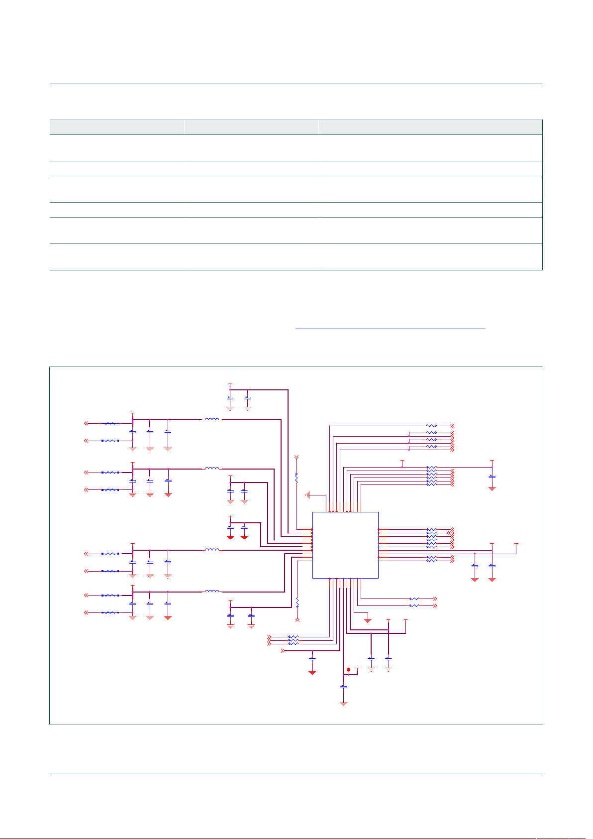
Figure 3. Primary PMIC reference
UM11374 All information provided in this document is subject to legal disclaimers. © NXP B.V. 2020. All rights reserved.
User manual Rev. 1 — 30 June 2020
7 / 26
Page 8
NXP Semiconductors
NOTE:
Replace the zero ohms with a small
sense resistor to measure the input
current for each switcher
INPUT SUPPLY
POWER GENERATION
External VDDIO
Vout = 1.242V x ( R2/R1 + 1)
VDDIO VOLTAGE OPTIONS
DEFAULT JUMPER SELECTION:
J55: 2-3
Close to U4
SW1_IN
SW2_IN
SW3_IN
SW4_IN
LDO_IN
VIN_IN
VIN
VIN
VIN_M
VIN
VDDIO
ADJ_FB
IIN_SNS_P 6
IIN_SNS_N 6
VIN_SNS_N 6
VIN_SNS_P 6
SH23
0
TP62
R95 0
C5
470PF
J55
HDR_1X3
1
2
3
R40
0
R193
76.8K
TP66
SH24
0
TP65
R90
0.01
R47
0
+
C6
2.2UF
J4
SKT BLACK
SILK = GND
1
2
TP80
R91 0
R93 0
J10
SKT RED
SILK = VIN
1
2
C115
47uF
SH1
0
R44
280K
TP64
TP63
SH22
0
C93
4.7uF
U4
MIC5205
IN
1
GND
2
ADJ
4
EN
3
OUT
5
R42
169K
TP67
R85 0
R92 0
R94 0
TP81
ADJ_FB
UM11374
KITPF5023FRDMEVM evaluation board
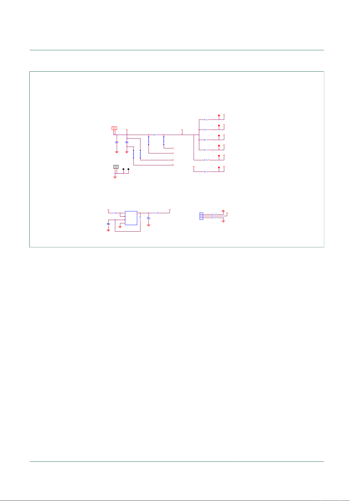
Figure 4. Power generation
UM11374 All information provided in this document is subject to legal disclaimers. © NXP B.V. 2020. All rights reserved.
User manual Rev. 1 — 30 June 2020
8 / 26
Page 9

NXP Semiconductors
Level /EdgeMode
ENABLE1 ENABLE2 ENABLE3 ENABLE4 XFAILB
PGOOD1 PGOOD2 PGOOD3 PGOOD4 PGOOD_IC
VDDOTP TBBEN STANDBY WDI
PULL-UPS, POWER GOODS AND STATUS INDICATORS
PWRON I2C INTB RESETBMCU
DEFAULT JUMPER SELECTION:
J39: 1-2
J40: Open
J41: Open
J42: Open
DEFAULT JUMPER SELECTION:
J34: 1-2
VIN
VDDIO
VDDIO
VDDIO
VDDIO
V1P5D_OUT
V1P5D_OUT
VDDIO
VDDIO
VIN
VDDIO
VIN
VDDIO
VIN
VDDIO
VIN
VDDIO
VIN
V1P5A_OUT
V1P5D_OUT
VIN
VIN
VIN
VIN
SCL3,7
RESETBMCU3,7
INTB3,7
VDDOTP 3
STANDBY 3,7
WDI 3,7
PGOOD13,7
PGOOD23,7
PGOOD33,7
PGOOD43
PGOOD3,7
XFAILB3,7
TBBEN 3,7
EN13,7
EN23,7
EN33,7
EN43,7
PWRON 3
PWRON_IC 3,6,7
SDA3,7
R148
100K
R103
100K
TP94
Q4
NX3008NBKW,115
1
2
3
ON
ON
SW12
SPDT_SWITCH
2
1
3
Q2
NX3008NBKW,115
1
2
3
R150
100K
R194
10K
R139
1.5K
R127
1.5K
R162
2.2K
J34
HDR_1X3
1
2
3
R130
1.5K
R136
1.5K
ON
ON
SW13
SPDT_SWITCH
2
1
3
R132
100K
D5
LED/GRN
A
C
SW3
FSMSM
1
2
Q6
NX3008NBKW,115
1
2
3
R126
100K
R147
100K
Q3
NX3008NBKW,115
1
2
3
Q5
NX3008NBKW,115
1
2
3
TP102
C79
1000pF
J39
HDR_1X3
1
2
3
R134
510K
D7
LED/GRN
A
C
R128
510K
TP93
R138
100K
ON
ON
SW10
SPDT_SWITCH
2
1
3
R145
100K
R129
100K
R135
100K
DNP
D4
LED/GRN
A
C
D6
LED/GRN
A
C
D3
LED/GRN
A
C
R109
2.2K
C130
0.01uF
DNP
R149
100K
R117
100K
C81
1000pF
TP103
J41
HDR_1X3
1
2
3
C80
1000pF
C77
1000pF
R140
510K
R133
1.5K
J42
HDR_1X3
1
2
3
C82
0.01uf
C78
1000pF
ON
ON
SW17
SPDT_SWITCH
2
1
3
ON
ON
SW11
SPDT_SWITCH
2
1
3
R131
510K
R137
510K
J40
HDR_1X3
1
2
3
UM11374
KITPF5023FRDMEVM evaluation board
Figure 5. Pull-ups, power goods, and status indicators
UM11374 All information provided in this document is subject to legal disclaimers. © NXP B.V. 2020. All rights reserved.
User manual Rev. 1 — 30 June 2020
9 / 26
Page 10

NXP Semiconductors
Layout note:
Place the resistors and the test points on the top
close to the load connectors
LOAD CONNECTIONS
LOAD CONFIGURATION
Dual phase options: Short SJ3 and SJ1, SJ4 and SJ6
Remove short on SJ2, SJ5
DEFAULT SOLDER BLOB
SELECTION: Short SJ1, SJ2, SJ4, SJ5
Dual Phase Output Dual Phase Output
Quad Phase Output: Short SJ7
NOTE (review):
Use below TPs for stability measurement
TP109, TP110 (SW1)
TP111, TP112 (SW2)
TP113, TP114 (SW3)
TP117, TP118 (SW4)
SW FEEDBACK OPTIONS
DEFAULT JUMPER SELECTION:
J62: 2-3
J63: 2-3
J64: 2-3
J65: 2-3
SW2_DUAL_OU T
SW1_DUAL_OU T
SW3_DUAL_OU T
SW4_DUAL_OU T
SW1_OUT
SW2_OUT
SW2_DUAL_OU T
SW1_DUAL_OU T
SW1_DUAL_OU T
SW3_DUAL_OU T
SW4_DUAL_OU T
SW3_OUT
SW4_OUT
SW3_DUAL_OU T
SW1_DUAL_OU T
SW2_DUAL_OU T
SW3_OUT
SW4_OUT
SW1_IOUT_P6
SW1_IOUT_N6
SW4_IOUT_P6
SW4_IOUT_N6
SW3_IOUT_P6
SW3_IOUT_N6
SW2_IOUT_P6
SW2_IOUT_N6
SW1_FB 3
SW1_OUT_EF FP 3,6
SW2_FB 3
SW2_OUT_EF FP 3,6
SW3_FB 3
SW3_OUT_EF FP 3,6
SW4_FB 3
SW4_OUT_EF FP 3,6
TP118
TP114
C113
22uF
DNP
TP112
TP77
TP69
SH29
0
SH25
0
TP110
SJ5
1
2
C109
22uF
DNP
R178 0.01
TP97
J32
TB_1X2
A
1
B
2
C110
22uF
DNP
0 0 0
SJ1
1
2
TP115
SJ7
1
2
J33
TB_1X2
A
1
B
2
SH28
0
J31
TB_1X2
A
1
B
2
SJ4
1
2
R191
0
SJ3
1
2
SH27
0
C111
22uF
DNP
TP76
R190
0
TP117
R189
0
R180 0.01
TP113
J65
HDR_1X3
1
2
3
SJ6
1
2
J64
HDR_1X3
1
2
3
TP111
J63
HDR_1X3
1
2
3
SH30
0
C114
22uF
DNP
SH40
0
R181 0.01
TP109
TP116
J62
HDR_1X3
1
2
3
R179 0.01
R192
0
SJ2
1
2
C120
22uF
DNP
SH26
0
C112
22uF
DNP
J61
TB_1X2
A
1
B
2
SH39
0
C121
22uF
DNP
SW1_FB_SEL
SW1_OUT_EF FP
SW2_FB_SEL
SW2_OUT_EF FP
SW3_FB_SEL
SW3_OUT_EF FP
SW4_FB_SEL
SW4_OUT_EF FP
UM11374
KITPF5023FRDMEVM evaluation board
Figure 6. Load configurations
UM11374 All information provided in this document is subject to legal disclaimers. © NXP B.V. 2020. All rights reserved.
User manual Rev. 1 — 30 June 2020
10 / 26
Page 11

NXP Semiconductors
PHASE VOLTAGE
PHASE CURRENT
INPUT VOLTAGE & CURRENT
MASTER/SLAVE CONNECTOR EFFICIENCY HEADER
AMUX/DMUX
SIGNALS/POWER
TEST POINTS AND TEST MODE HEADERS
AMUX/DMUX
JTAG
NOTE: Use single 12 Row connector to connect
Slave side from primary EVB to Master side of 2nd
EVB. Resistors can be configured on primary board
for specific configurations.
VDDIO_IC
V1P5D_OUT
V1P5A_OUT
SW1_OUT_EF FP3,5
SW1_OUT_EF FN3
SW2_OUT_EF FP3,5
SW2_OUT_EF FN3
SW3_OUT_EF FP3,5
SW3_OUT_EF FN3
IIN_SNS_P2
IIN_SNS_N2
SW1_IOUT_P5
SW1_IOUT_N5
SW2_IOUT_P5
SW2_IOUT_N5
SW3_IOUT_P5
SW3_IOUT_N5
VIN_SNS_P2
VIN_SNS_N2
SW4_OUT_EF FP3,5
SW4_OUT_EF FN3
SW4_IOUT_P5
SW4_IOUT_N5
SW1_OUT_EF FP_FLT 6
SW1_OUT_EF FN_FLT 6
SW2_OUT_EF FN_FLT 6
SW2_OUT_EF FP_FLT 6
SW3_OUT_EF FP_FLT 6
SW3_OUT_EF FN_FLT 6
IIN_SNS_N_FLT 6
IIN_SNS_P_FLT 6
SW1_IOUT_N_F LT 6
SW1_IOUT_P_FLT 6
SW2_IOUT_N_F LT 6
SW2_IOUT_P_FLT 6
SW3_IOUT_N_F LT 6
SW3_IOUT_P_FLT 6
SW4_OUT_EF FP_FLT 6
SW4_OUT_EF FN_FLT 6
VIN_SNS_N_FLT 6
VIN_SNS_P_FLT 6
SW4_IOUT_N_F LT 6
SW4_IOUT_P_FLT 6
VIN_SNS_P_FLT6
VIN_SNS_N_FLT 6
RESETBMCU_IC3,6
IIN_SNS_P_FLT6
IIN_SNS_N_FLT 6
INTB_IC3,6
SW1_OUT_EF FP_FLT6
SW1_OUT_EF FN_FLT 6
SW1_IOUT_P_FLT6
SW1_IOUT_N_F LT 6
SYNCOUT_IC3,6
SW2_OUT_EF FP_FLT6
SW2_OUT_EF FN_FLT 6
INTB_IC3,6
SW2_IOUT_P_FLT6
SW2_IOUT_N_F LT 6
WDI_IC3,6
SW3_OUT_EF FP_FLT6
SW3_OUT_EF FN_FLT 6
PWRON_IC3,4,6,7
SW3_IOUT_P_FLT6
SW3_IOUT_N_F LT 6
STANDBY_IC3,6
SCL_IC3
TELEM_OUT_17
SDA_IC3
TELEM_OUT_27
XFAILB_IC3,6
SW4_OUT_EF FP_FLT6
SW4_OUT_EF FN_FLT 6
PGOOD_IC3,6
SW4_IOUT_P_FLT6
SW4_IOUT_N_F LT 6
EN1_IC3
INTB_IC3,6
EN3_IC3
PGOOD_IC3,6
PGOOD3_IC3
PGOOD1_IC3,6
EN2_IC3
PGOOD2_IC3,6
WDI_IC3 ,6
WDI_IC3,6
EN4_IC3
INTB_IC3,6
PGOOD4_IC3
PGOOD_IC3,6
PWRON_IC3,4,6,7
PGOOD1_IC3,6
PGOOD2_IC3,6
PGOOD2_IC3,6
RESETBMCU_IC3,6
WDI_IC3,6
SYNCOUT_IC3,6
STANDBY_IC3,6
XFAILB_IC3,6
VSNVS_OUT3
R17 1.00k
C90
1uF
TP88
J70
HDR_2X12
1
2
3
4
6
5
7
8
9
10
11
12
13
14
15
16
17
18
19
20
21
22
23
24
TP92
R170 1.00k
R175 1.00k
R187 1.00k
TP107
R174 1.00k
R168 1.00k
R188 1.00k
C89
1uF
R165 1.00k
R166 1.00k
C91
1uF
C98
1uF
J68
HDR_2X5
1
2
3
4
6
5
7
8
9
10
R171 1.00k
R159 1.00k
J71
HDR_2X5
1
2
3
4
6
5
7
8
9
10
TP106
R158 1.00k
J66
HDR_2X13
1
2
3
4
6
5
7
8
9
10
11
12
13
14
15
16
17
18
19
20
21
22
23
24
25
26
C97
1uF
R186 1.00k
C128
1uF
R169 1.00k
R185 1.00k
C101
1uF
J69
HDR_2X5
1
2
3
4
6
5
7
8
9
10
C129
1uF
C96
1uF
R156 1.00k
R155 1.00k
C95
1uF
R167 1.00k
R172 1.00k
TP90
R157 1.00k
TP91
J67
HDR_2X12
1
2
3
4
6
5
7
8
9
10
11
12
13
14
15
16
17
18
19
20
21
22
23
24
TP89
SW1_OUT_EF FP_FLT
SW1_OUT_EF FN_FLT
SW2_OUT_EF FP_FLT
SW2_OUT_EF FN_FLT
SW3_OUT_EF FP_FLT
SW3_OUT_EF FN_FLT
IIN_SNS_P_FLT
IIN_SNS_N_FLT
SW1_IOUT_P_FLT
SW1_IOUT_N_F LT
SW2_IOUT_P_FLT
SW2_IOUT_N_F LT
SW3_IOUT_P_FLT
SW3_IOUT_N_F LT
VIN_SNS_P_FLT
VIN_SNS_N_FLT
SW4_OUT_EF FN_FLT
SW4_IOUT_P_FLT
SW4_IOUT_N_F LT
SW4_OUT_EF FP_FLT
RESETBMCU_IC
INTB_IC
SYNCOUT_IC
INTB_IC
WDI_IC
PWRON_IC
STANDBY_IC
SCL_IC
SDA_IC
XFAILB_IC
PGOOD_IC
EN1_IC
INTB_IC
EN3_IC
PGOOD_IC
PGOOD3_IC
PGOOD1_IC
EN2_IC
PGOOD2_IC
WDI_IC
WDI_IC
EN4_IC
INTB_IC
PGOOD4_IC
PGOOD_IC
PWRON_IC
PGOOD1_IC
PGOOD2_IC
PGOOD2_IC
RESETBMCU_IC
WDI_IC
SYNCOUT_IC
STANDBY_IC
XFAILB_IC
VSNVS_OUT
UM11374
KITPF5023FRDMEVM evaluation board
Figure 7. Signal and power measurement
UM11374 All information provided in this document is subject to legal disclaimers. © NXP B.V. 2020. All rights reserved.
User manual Rev. 1 — 30 June 2020
11 / 26
Page 12

NXP Semiconductors
(PTC7)
(TRST_B/PTC0)
(PTC3)
(PTC4)
(PTC5)
(PTC6)
(PTC10)
(PTC11)
(TCK/PTE0)
(VREF)
(PTD1)
(PTD3)
(TMS/PTD2)
(PTD0)
(PTD5)
(PTA13)
(PTC9)
(PTC8)
(TDI/PTA5)
(PTA4)
(PTA12)
(PTD4)
(PTA2)
(PTA1)
(TDO/PTC12)
(PTC13)
(PTC16)
(PTC17)
(PTA16)
(PTA17)
(PTE31)
(PTD6)
(PTD7)
(PTE30)
(PTE29)
(PTE23)
(PTE22)
(PTE21)
(PTE20)
(PTC1)
(PTC2)
(PTB3)
(PTB2)
(PTB1)
(PTB0)
(5V)
(3V3)
(3V3)
ADC4
ADC5
(PTE1)
(GND)
(NC)
(P5-9V_VIN)
(GND)
(GND)
(PTA20)
(SDA/PTD5)
Mates with SSQ-106-23-G-D
Mates SSQ-108-23-G-D
Mates SSQ-110-23-G-D
Mates SSQ-108-23-G-D
(PTE5)
(PTE4)
(PTE3)
(PTE2)
(PTB11)
(PTB10)
(PTB9)
(PTB8)
KL25Z
Feemale connectors on the Freedom board
with long pins, low insertion:
SSQ-106-23-G-D / 210-80515
SSQ-110-23-G-D / 210-80513
SSQ-108-23-G-D (x2) / 210-80247
P3V3_FRDM
P5V_USB
RESETBMCU3,4
PGOOD3,4
TELEM_OUT_1 6
STANDBY 3,4
TELEM_OUT_2 6
PGOOD1 3,4
PGOOD3 3,4
INTB 3,4
XFAILB 3,4
EN23,4
EN43,4
SCL3,4
SDA3,4
EN33,4
PGOOD2 3,4
PWRON _IC3,4,6
WDI 3,4
TBBEN3,4
SYNCOUT3
EN1 3,4
J1
CON 2X8
2
4
6
8
10
12
14
16
1
3
5
7
9
11
13
15
J5
CON 2X6 SKT
1
2
3
4
6
5
7
8
9
10
11
12
J2
CON_2X10
1
2
3
4
6
5
7
8
9
10
11
12
13
14
15
16
17
18
19
20
J6
CON 2X8
2
4
6
8
10
12
14
16
1
3
5
7
9
11
13
15
TP17
TP13
UM11374
KITPF5023FRDMEVM evaluation board
Figure 8. FRDM-KL25Z interface
4.3.2 Board layout
Figure 9. Top
UM11374 All information provided in this document is subject to legal disclaimers. © NXP B.V. 2020. All rights reserved.
User manual Rev. 1 — 30 June 2020
12 / 26
Page 13

NXP Semiconductors
UM11374
KITPF5023FRDMEVM evaluation board
Figure 10. Layer 2
Figure 11. Layer 3
UM11374 All information provided in this document is subject to legal disclaimers. © NXP B.V. 2020. All rights reserved.
User manual Rev. 1 — 30 June 2020
13 / 26
Page 14

NXP Semiconductors
UM11374
KITPF5023FRDMEVM evaluation board
Figure 12. Layer 4
UM11374 All information provided in this document is subject to legal disclaimers. © NXP B.V. 2020. All rights reserved.
User manual Rev. 1 — 30 June 2020
14 / 26
Page 15

NXP Semiconductors
UM11374
KITPF5023FRDMEVM evaluation board
Figure 13. Layer 5
Figure 14. Bottom
UM11374 All information provided in this document is subject to legal disclaimers. © NXP B.V. 2020. All rights reserved.
User manual Rev. 1 — 30 June 2020
15 / 26
Page 16

NXP Semiconductors
UM11374
KITPF5023FRDMEVM evaluation board
4.3.3 Bill of Materials
Table 2. Bill of Materials
NXP does not assume liability, endorse, or warrant components from external manufacturers are referenced in circuit
drawings or tables. While NXP offers component recommendations in this configuration, it is the customer’s responsibility to
validate their application.
DNP: do not populate
For critical components, it is vital to use the manufacturer listed.
Item
Quan
number
Active components
1 1 U4 MIC5205 IC LIN VREG LDO 1.5 V to 15 V 150 mA 2.5 V to 16 V
2 1 U9 MPF5023AMBA0ES IC POWER MANAGEMENT 5.5 V AEC-Q100 QFN40 MPF5023AMBA0ES NXP
Capacitors
3 1 C5 470 pF CAP CER 470 pF 50 V 5 % COG 0603 06035A471JAT2A AVX
4 1 C6 2.2 µF CAP TANT ESR = 1.800 Ω 2.2 µF 10 V 10 % 3216-18 TPSA225K010R1800 AVX
5 16 C59, C104, C105, C106, C107,C108, C109,
6 6 C61, C93, C102, C103, C124, C127 4.7 µF CAP CER 4.7 µF 16 V 10 % X7R AEC-Q200 0805 CGA4J3X7R1C475K125AB TDK
7 8 C62, C64, C68, C125, C131, C132,C133,
8 15 C71, C74, C75, C76, C89, C90, C91, C95,
9 1 C72 2.2 µF CAP CER 2.2 µF 10 V 10 % X7S AEC-Q200 0402 GRT155C71A225KE13 MURATA
10 5 C77, C78, C79, C80, C81 1000 pF CAP CER 1000 pF 50 V 5 % C0G AEC-Q200 0603 CGA3E2C0G1H102J080AA TDK
11 1 C82 0.01 µF CAP CER 0.01 µF 50 V 10 % X7R AEC-Q200 0603 CGA3E2X7R1H103K080AA TDK
12 1 C115 47 µF CAP CER 47 µF 10 V 20 % X5R AEC-Q200 1206 GRT31CR61A476ME13L MURATA
13 1 C130 0.01 µF CAP CER 0.01 µF 50 V 10 % X7R AEC-Q200 0402 GCM155R71H103KA55D MURATA DNP
Diodes
14 5 D3, D4, D5, D6, D7 LED/GRN LED GRN SGL 20 mA SMT NRND LP M67K-E2G1-25 OSRAM
Resistors
15 20 R17, R155, R156, R157, R158, R159, R165,
16 31 R40, R47, R104, R105, R106, R107, R108,
17 1 R42 169 kΩ RES MF 169 kΩ 1/10 W 1 % AEC-Q200 0603 RK73H1JTTD1693F KOA SPEER
18 1 R44 280 kΩ RES MF 280 kΩ 1/10 W 1 % AEC-Q200 0402 RK73H1ETTP2803F KOA SPEER
19 6 R85, R91, R92, R93, R94, R95 0 Ω RES MF ZERO 1/8 W AEC-Q200 0805 MCR10EZPJ000 ROHM
20 5 R90, R178, R179, R180, R181 0.01 Ω RES TF 0.01 Ω 1 W 1 % AEC-Q200 1206 ERJ-8CWFR010V PANASONIC
21 12 R103, R117, R126, R129, R132, R135,
22 2 R109, R162 2.2 kΩ RES MF 2.2 kΩ 1/16 W 0.1 % AEC-Q200 0402 ERA-2AEB222X PANASONIC
23 5 R127, R130, R133, R136, R139 1.5 kΩ RES MF 1.5 kΩ 1/10 W 5 % AEC-Q200 0603 ERJ3GEYJ152V PANASONIC
24 5 R128, R131, R134, R137, R140 510 kΩ RES MF 510 kΩ 1/10 W 5 % 0603 RC0603JR-07510KL YAGEO AMERICA
25 1 R193 76.8 kΩ RES MF 76.8 kΩ 1/10 W 1 % AEC-Q200 0402 RK73H1ETTP7682F KOA SPEER
26 1 R194 10 kΩ RES MF 10 kΩ 5 % 1/10 W AEC-Q200 0402 ERJ-2GEJ103X PANASONIC
Switches, Connectors, Jumpers, and Test Points
27 2 J1, J6 CON 2X8 CON 2X8 SKT TH 100 MIL SP 335H AU 104L SSW-108-01-S-D SAMTEC
28 1 J2 CON_2X10 CON 2X10 SKT TH 100 MIL CTR 340H AU 104L SSW-110-01-G-D SAMTEC
29 1 J4 SKT BLACK CON 1X2 BANANA BLACK RA TH 15.3 MM SP 492H AG
30 1 J5 CON 2X6 SKT CON 2X6 SKT TH 100 MIL CTR 340H AU 104L SSW-106-01-G-D SAMTEC
31 1 J10 SKT RED CON 1X2 BANANA RED RA TH 15.3MM SP 488H AG 197L 571-0500 DELTRON EMCON
32 4 J31, J32, J33, J61 TB_1X2 CON 1X2 TB TH 5 MM SP 398H SN 138L 691102710002 WURTH
33 10 J34, J39, J40, J41, J42, J55, J62, J63, J64,
34 1 J66 HDR_2X13 HDR 2X13 TH 100 MIL CTR 330H AU TSW-113-07-S-D SAMTEC
35 2 J67, J70 HDR_2X12 HDR 2X12 TH 100 MIL CTR 337H AU 100L TSW-112-07-G-D SAMTEC
UM11374 All information provided in this document is subject to legal disclaimers. © NXP B.V. 2020. All rights reserved.
User manual Rev. 1 — 30 June 2020
Schematic label Value Description Part number Manufacturer name Assy
tity
MIC5205YM5 MICREL
SEMICONDUCTORS
INTERTECHNOLOGY
571-0100 DELTRON EMCON
LTD
LTD
ELEKTRONIK EISOS
GMBH & CO. KG
C110, C111, C112,C113, C114, C120,C121,
C122,C123
C134
C96, C97, C98, C101,C128, C129, C135
R166, R167, R168, R169, R170, R171,
R172, R174, R175, R185, R186, R187,
R188
R112, R113, R114, R115, R116, R118,
R119, R120, R121, R122, R123, R124,
R125, R141, R142, R143, R144, R176,
R177, R182, R189, R190, R191, R192
R138, R145, R147, R148, R149, R150
J65
SOT23-5
22 µF CAP CER 22 µF 10 V 10 % X7R AEC-Q200 1206 LMJ316BB7226KLHT Taiyo Yuden
0.1 µF CAP CER 0.1 µF 16 V 10 % X7R AEC-Q200 0402 GCM155R71C104KA55D MURATA
1.0 µF CAP CER 1 µF 10 V 10 % X7S AEC-Q200 0402 GCM155C71A105KE38D MURATA
1.00 kΩ RES MF 1.00 kΩ 1/16 W 1 % AEC-Q200 0402 RK73H1ETTP1001F KOA SPEER
0 Ω RES MF ZERO Ω 1/16 W -- AEC-Q200 0402 CRCW04020000Z0ED VISHAY
100 kΩ RES MF 100 kΩ 1 % 1/10 W AEC-Q200 0402 ERJ-2RKF1003X PANASONIC
197L
HDR_1X3 HDR 1X3 TH 100MIL SP 330H AU 98L HTSW-103-07-S-S SAMTEC
Opt
16 / 26
Page 17

NXP Semiconductors
UM11374
KITPF5023FRDMEVM evaluation board
Item
Quan
number
36 3 J68, J69, J71 HDR_2X5 HDR 2X5 TH 100MIL CTR 330H AU TSW-105-08-G-D SAMTEC
37 4 L8, L9, L10, L11 1.0 µH IND PWR 1.0 µH@1 MHZ 4.7A 20 % AEC-Q200 SMD TFM252012ALMA1R0MTAA TDK
38 5 Q2, Q3, Q4, Q5, Q6 NX3008NBKW, 115 TRAN NMOS SW 30 V 350 mA AEC-Q101 SC-70 NX3008NBKW, 115 NEXPERIA
39 20 SH1, SH22, SH23, SH24, SH25, SH26,
40 7 SJ1, SJ2, SJ3, SJ4, SJ5, SJ6, SJ7 0402 JUMPER SOLDER BLOB JUMPER 0402 OPEN NO PART TO
41 1 SW3 FSMSM SW SPST PB 12 V 50 mA SMT 1437566-4 Tyco Electronics
42 5 SW10, SW11, SW12, SW13, SW17 SPDT_SWITCH SW SPDT SLIDE 0.1 A 12 V TH OS102011MS2QN1 C&K Components
43 2 TP13, TP17 TPAD_030 TEST POINT PAD 30 MIL DIA SMT, NO PART TO ORDER NOT A COMPONENT NOT A COMPONENT
44 19 TP62, TP63, TP64, TP65, TP66, TP67,
45 15 TP69, TP76, TP77, TP80, TP81, TP88,
Schematic label Value Description Part number Manufacturer name Assy
tity
SH27, SH28, SH29, SH30, SH31, SH32,
SH33, SH34, SH35, SH36, SH39, SH40,
SH42, SH43
TP93, TP94, TP102, TP103, TP108, TP109,
TP110, TP111, TP112, TP113, TP114,
TP117, TP118
TP89, TP90, TP91, TP92, TP97, TP106,
TP107, TP115, TP116
0 ZERO Ω CUT TRACE 0201 PADS; NO PART TO ORDER LAYOUT ELEMENT ONLY LAYOUT ELEMENT
ORDER
TESTLOOP_RED TEST POINT PC MULTI PURPOSE RED TH 5010 KEYSTONE
TESTLOOP_BLACK TEST POINT PC MULTI PURPOSE BLK TH 5011 KEYSTONE
NA NA
ONLY
ELECTRONICS
ELECTRONICS
5 Installing and configuring software and tools
Download and unzip the NXP_GUI_ PR_1.0 file into any desired location. The package
should contain a GUI folder and MCU folder.
Opt
5.1 Freedom board BOOTLOADER refresh in a Windows 7 or 10 system (optional - only when the Freedom board is not preprogrammed)
1. Press the RST push button on the Freedom board and connect the USB cable into the
SDA port on the Freedom board. A new BOOTLOADER device should appear on the
left pane of the File explorer.
2. Drag and drop the file MSD-DEBUG-FRDM-KL25Z_Pemicro_v118.SDA from the
MCU folder into the BOOTLOADER drive.
Note: Make sure to allow enough time for the firmware to be saved in the Bootloader.
UM11374 All information provided in this document is subject to legal disclaimers. © NXP B.V. 2020. All rights reserved.
User manual Rev. 1 — 30 June 2020
17 / 26
Page 18

NXP Semiconductors
3. Disconnect and reconnect the USB cable into the SDA port (this time without pressing
the RST push button). The PC installs a new device called FRDM_KL25Z.
4. Locate the file nxp-gui-fw-frdmkl25z-usb_hid-pf502x_v0.1.6.bin from the MCU
folder and drag and drop the file into the FRDM_KL25Z device.
5. Freedom board firmware is successfully loaded.
6. Open and run the NXP_GUI-1.0-Setup.exe file from the GUI folder inside the
unzipped package. This installs the NXPGUI software in the system. Install it in a local
destination folder.
6 Configuring the hardware for startup
To configure the hardware and workstation, complete the following procedure:
1. With the USB cable connected to the PC and the USB port in the freedom board,
apply VIN to the evaluation board.
a. Provide external VIN between 2.5 V to 5.5 V on J10 (VIN) and J4 (GND). Make
sure that the supply is current limited to 100 mA.
2. Press Reset on the Freedom board, to ensure board is properly recognized.
3. If the NXPGUI application was not installed before, perform step 6 of Section 5.1
"Freedom board BOOTLOADER refresh in a Windows 7 or 10 system (optional - only
when the Freedom board is not preprogrammed)" to install it for the first time. Open
the NXPGUI application from the installation folder or from the Start menu.
4. A configuration window is displayed. Select one of the devices to load the predefined
configurations, and then click OK.
UM11374
KITPF5023FRDMEVM evaluation board
UM11374 All information provided in this document is subject to legal disclaimers. © NXP B.V. 2020. All rights reserved.
User manual Rev. 1 — 30 June 2020
18 / 26
Page 19

NXP Semiconductors
UM11374
KITPF5023FRDMEVM evaluation board
5. The NXPGUI interface should open and load the main framework. Make sure to
confirm if the GUI can identify the USB device properly. This is displayed by the active
Start button on the top-left corner of the GUI.
Note: The USB cable should be connected for the GUI to recognize and be able to
connect to the device.
6. Click Start to enable the connection to the device. The device status can be read from
the bottom-left corner of the GUI.
7. Once the device is connected, the system is ready for Hardwire, TBB or OTP
operation as desired.
UM11374 All information provided in this document is subject to legal disclaimers. © NXP B.V. 2020. All rights reserved.
User manual Rev. 1 — 30 June 2020
19 / 26
Page 20

NXP Semiconductors
KITPF5023FRDMEVM evaluation board
7 Using the KITPF5023FRDMEVM evaluation board
This section summarizes the overall setup. Detailed description is provided in the
following sections.
7.1 Operating in Hardwire mode
To operate the board with the default hardwire configuration, complete the following
procedure:
1. Short J34 in position 2-3 and SW17 in position 1 (PWRON = high) or leave J34 open
to let the MCU on the board control the pin.
2. Short J39 in position 2-3 (VDDOTP = V1P5D).
3. Short J40 in position 1-2 (TBBEN = Low).
In Hardwire mode, applying power to the board turns On the device by default. However,
when the GUI is started, and the device is connected, the PMIC turn On/Off can be
controlled via the PWRON control in the IO Pins tab of the main window.
UM11374
7.2 Operating in TBB mode
To operate the device in TBB mode, an TBB script can be created using the OTP section
of the NXPGUI (installed in the previous steps).
To generate a TBB script, complete the following procedure:
1. Select the configuration settings in the OTP tool as required.
2. Generate a TBB script using the Export section on the OTP tool (make sure to fill all
required fields marked with a * next to them). Save the generated TBB file in a known
location.
UM11374 All information provided in this document is subject to legal disclaimers. © NXP B.V. 2020. All rights reserved.
User manual Rev. 1 — 30 June 2020
20 / 26
Page 21

NXP Semiconductors
UM11374
KITPF5023FRDMEVM evaluation board
To operate the board in TBB mode, complete the following procedure:
1. Set SW17 to position to 3 (PWRON to GND).
2. Short J40 in position 2-3 (TBB = V1P5D).
Or
3. Use the NXPGUI to select the TBB mode, when the KL25Z interface board is
connected to the EVB. Disconnect jumpers J40, J34, J41, and J42 from the board as
explained in Section 4.2.2 "Jumper, switch, and shunt configuration".
4. In the Script section of the GUI, use the command window to load the TBB script
created and click Run to start programming the PF5023.
5. After Script is done programming, the device is automatically enabled with the
selected TBB configuration.
7.3 Programming/burning OTP in TBB mode
To program the OTP, the device must be operated in TBB mode. An OTP script can be
created using the NXPGUI OTP section.
1. Start the NXPGUI from the installation folder or from the Start menu. Follow the steps
in Section 6 "Configuring the hardware for startup" to start the GUI and connect to the
board.
2. Generate the desired OTP configuration and the configuration using the file menu on
the top left.
UM11374 All information provided in this document is subject to legal disclaimers. © NXP B.V. 2020. All rights reserved.
User manual Rev. 1 — 30 June 2020
21 / 26
Page 22

NXP Semiconductors
3. Select OTP from the Export tab in the menu and save the generated OTP file(.txt) in
UM11374
KITPF5023FRDMEVM evaluation board
a known location with a desired filename.
4. To operate the board in TBB mode:
a. Follow step 3 in Section 7.2 "Operating in TBB mode".
b. Other jumpers must be in the configuration as explained in Section 4.2.2 "Jumper,
switch, and shunt configuration".
5. Remove jumper on J39 and connect an external supply of 8.0 V on the VDDOTP pin
at J39, pin2.
6. In the PROG section, use the Config Source button to select "script", and then click
the Browse button to load the config (*.cfg) file saved before. Click Program to start
programming the PF5023 device.
7. After the script completes the programming, the device is automatically enabled with
the selected OTP configuration. Remove the voltage on the VDDOTP pin (J39-2).
UM11374 All information provided in this document is subject to legal disclaimers. © NXP B.V. 2020. All rights reserved.
User manual Rev. 1 — 30 June 2020
22 / 26
Page 23

NXP Semiconductors
8. Put the jumper on J39 (1-2). Select user-mode in the GUI and click Apply to turn On
9. Turn Off the power supply and turn back-on to reconnect the device.
10.Using the IO Pins tab in the main window of the GUI, set the PWRON pin high
UM11374
KITPF5023FRDMEVM evaluation board
the board with new settings.
Or
to enable the device with the programmed configuration. Ensure that the enable
switches SW10, SW11, SW12 are set high for the regulators to turn On.
8 References
[1] KITPF5023FRDMEVM — detailed information on this board, including documentation, downloads, and software and
tools
http://www.nxp.com/KITPF5023FRDMEVM
[2] PF5023 — product information on PF5023, Power management integrated circuit (PMIC) for high performance
applications
http://www.nxp.com/PF5023
[3] FRDM-KL25Z — detailed information on this board, including documentation, downloads, and software and tools
https://www.nxp.com/FRDM-KL25Z
9 Revision history
Revision history
Rev Date Description
v.1 20200630 Initial version
UM11374 All information provided in this document is subject to legal disclaimers. © NXP B.V. 2020. All rights reserved.
User manual Rev. 1 — 30 June 2020
23 / 26
Page 24

NXP Semiconductors
10 Legal information
10.1 Definitions
UM11374
KITPF5023FRDMEVM evaluation board
default of the applications and the products or of the application or use by
customer’s third party customer(s). NXP does not accept any liability in this
respect.
Draft — The document is a draft version only. The content is still under
internal review and subject to formal approval, which may result in
modifications or additions. NXP Semiconductors does not give any
representations or warranties as to the accuracy or completeness of
information included herein and shall have no liability for the consequences
of use of such information.
10.2 Disclaimers
Limited warranty and liability — Information in this document is believed
to be accurate and reliable. However, NXP Semiconductors does not
give any representations or warranties, expressed or implied, as to the
accuracy or completeness of such information and shall have no liability
for the consequences of use of such information. NXP Semiconductors
takes no responsibility for the content in this document if provided by an
information source outside of NXP Semiconductors. In no event shall NXP
Semiconductors be liable for any indirect, incidental, punitive, special or
consequential damages (including - without limitation - lost profits, lost
savings, business interruption, costs related to the removal or replacement
of any products or rework charges) whether or not such damages are based
on tort (including negligence), warranty, breach of contract or any other
legal theory. Notwithstanding any damages that customer might incur for
any reason whatsoever, NXP Semiconductors’ aggregate and cumulative
liability towards customer for the products described herein shall be limited
in accordance with the Terms and conditions of commercial sale of NXP
Semiconductors.
Right to make changes — NXP Semiconductors reserves the right to
make changes to information published in this document, including without
limitation specifications and product descriptions, at any time and without
notice. This document supersedes and replaces all information supplied prior
to the publication hereof.
Applications — Applications that are described herein for any of these
products are for illustrative purposes only. NXP Semiconductors makes
no representation or warranty that such applications will be suitable
for the specified use without further testing or modification. Customers
are responsible for the design and operation of their applications and
products using NXP Semiconductors products, and NXP Semiconductors
accepts no liability for any assistance with applications or customer product
design. It is customer’s sole responsibility to determine whether the NXP
Semiconductors product is suitable and fit for the customer’s applications
and products planned, as well as for the planned application and use of
customer’s third party customer(s). Customers should provide appropriate
design and operating safeguards to minimize the risks associated with
their applications and products. NXP Semiconductors does not accept any
liability related to any default, damage, costs or problem which is based
on any weakness or default in the customer’s applications or products, or
the application or use by customer’s third party customer(s). Customer is
responsible for doing all necessary testing for the customer’s applications
and products using NXP Semiconductors products in order to avoid a
Suitability for use in automotive applications — This NXP
Semiconductors product has been qualified for use in automotive
applications. Unless otherwise agreed in writing, the product is not designed,
authorized or warranted to be suitable for use in life support, life-critical or
safety-critical systems or equipment, nor in applications where failure or
malfunction of an NXP Semiconductors product can reasonably be expected
to result in personal injury, death or severe property or environmental
damage. NXP Semiconductors and its suppliers accept no liability for
inclusion and/or use of NXP Semiconductors products in such equipment or
applications and therefore such inclusion and/or use is at the customer's own
risk.
Export control — This document as well as the item(s) described herein
may be subject to export control regulations. Export might require a prior
authorization from competent authorities.
Evaluation products — This product is provided on an “as is” and “with all
faults” basis for evaluation purposes only. NXP Semiconductors, its affiliates
and their suppliers expressly disclaim all warranties, whether express,
implied or statutory, including but not limited to the implied warranties of
non-infringement, merchantability and fitness for a particular purpose. The
entire risk as to the quality, or arising out of the use or performance, of this
product remains with customer. In no event shall NXP Semiconductors, its
affiliates or their suppliers be liable to customer for any special, indirect,
consequential, punitive or incidental damages (including without limitation
damages for loss of business, business interruption, loss of use, loss of
data or information, and the like) arising out the use of or inability to use
the product, whether or not based on tort (including negligence), strict
liability, breach of contract, breach of warranty or any other theory, even if
advised of the possibility of such damages. Notwithstanding any damages
that customer might incur for any reason whatsoever (including without
limitation, all damages referenced above and all direct or general damages),
the entire liability of NXP Semiconductors, its affiliates and their suppliers
and customer’s exclusive remedy for all of the foregoing shall be limited to
actual damages incurred by customer based on reasonable reliance up to
the greater of the amount actually paid by customer for the product or five
dollars (US$5.00). The foregoing limitations, exclusions and disclaimers
shall apply to the maximum extent permitted by applicable law, even if any
remedy fails of its essential purpose.
Translations — A non-English (translated) version of a document is for
reference only. The English version shall prevail in case of any discrepancy
between the translated and English versions.
10.3 Trademarks
Notice: All referenced brands, product names, service names and
trademarks are the property of their respective owners.
NXP — is a trademark of NXP B.V.
SMARTMOS — is a trademark of NXP B.V.
UM11374 All information provided in this document is subject to legal disclaimers. © NXP B.V. 2020. All rights reserved.
User manual Rev. 1 — 30 June 2020
24 / 26
Page 25

NXP Semiconductors
Tables
UM11374
KITPF5023FRDMEVM evaluation board
Tab. 1. Evaluation board jumper, switch, and shunt
descriptions ....................................................... 6
Figures
Fig. 1. KITPF5023FRDMEVM ...................................... 1
Fig. 2. Evaluation board featured component
locations ............................................................ 5
Fig. 3. Primary PMIC reference ....................................7
Fig. 4. Power generation .............................................. 8
Fig. 5. Pull-ups, power goods, and status indicators .... 9
Fig. 6. Load configurations ......................................... 10
Fig. 7. Signal and power measurement ......................11
Tab. 2. Bill of Materials ................................................16
Fig. 8. FRDM-KL25Z interface ................................... 12
Fig. 9. Top .................................................................. 12
Fig. 10. Layer 2 ............................................................ 13
Fig. 11. Layer 3 ............................................................ 13
Fig. 12. Layer 4 ............................................................ 14
Fig. 13. Layer 5 ............................................................ 15
Fig. 14. Bottom ............................................................. 15
UM11374 All information provided in this document is subject to legal disclaimers. © NXP B.V. 2020. All rights reserved.
User manual Rev. 1 — 30 June 2020
25 / 26
Page 26

NXP Semiconductors
Contents
1 Introduction ......................................................... 3
2 Finding kit resources and information on
the NXP web site ................................................ 3
2.1 Collaborate in the NXP community ....................3
3 Getting ready .......................................................3
3.1 Kit contents ........................................................3
3.2 Additional hardware ........................................... 3
3.3 Windows PC workstation ................................... 3
3.4 Software .............................................................4
4 Getting to know the hardware ........................... 4
4.1 KITPF5023FRDMEVM features .........................4
4.2 Kit featured components ....................................5
4.2.1 PF5023: Power management integrated
circuit (PMIC) for high performance
applications ........................................................ 5
4.2.1.1 General description ............................................5
4.2.1.2 Features .............................................................6
4.2.2 Jumper, switch, and shunt configuration ............6
4.3 Schematic, board layout and bill of materials .....7
4.3.1 Schematics ........................................................ 7
4.3.2 Board layout .................................................... 12
4.3.3 Bill of Materials ................................................ 16
5 Installing and configuring software and
tools ....................................................................17
5.1 Freedom board BOOTLOADER refresh in
a Windows 7 or 10 system (optional only when the Freedom board is not
preprogrammed) .............................................. 17
6 Configuring the hardware for startup ..............18
7 Using the KITPF5023FRDMEVM evaluation
board .................................................................. 20
7.1 Operating in Hardwire mode ............................20
7.2 Operating in TBB mode ................................... 20
7.3 Programming/burning OTP in TBB mode ........ 21
8 References ......................................................... 23
9 Revision history ................................................ 23
10 Legal information .............................................. 24
UM11374
KITPF5023FRDMEVM evaluation board
Please be aware that important notices concerning this document and the product(s)
described herein, have been included in section 'Legal information'.
© NXP B.V. 2020. All rights reserved.
For more information, please visit: http://www.nxp.com
For sales office addresses, please send an email to: salesaddresses@nxp.com
Date of release: 30 June 2020
Document identifier: UM11374
 Loading...