

NXP KITFS4503CAEEVM, KITFS4508CAEEVM, KITFS6507LAEEVM, KITFS6522LAEEVM, KITFS6523CAEEVM User Manual
Page 1
NXP Semiconductors
User manual
Document Number: KTFS4500-FS6500UG
Rev. 2, 3/2021
KITFS4503CAEEVM, KITFS4508CAEEVM,
KITFS6507LAEEVM, KITFS6522LAEEVM, and
KITFS6523CAEEVM evaluation boards
© NXP B.V. 2021.
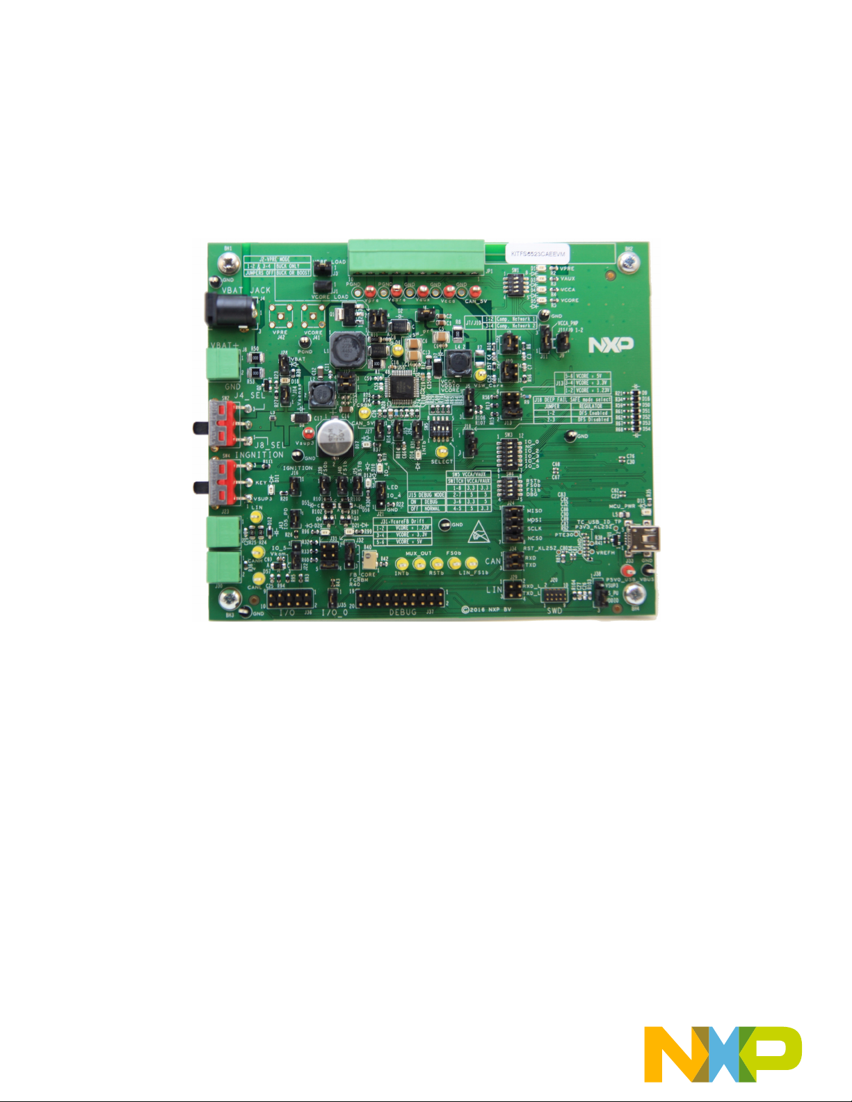
Figure 1. FS45xx/FS65xx evaluation board
Page 2

Contents
1 Getting started. . . . . . . . . . . . . . . . . . . . . . . . . . . . . . . . . . . . . . . . . . . . . . . . . . . . . . . . . . . . . . . . . . . . . . . . . . . . . . . . . . . . . . . . . . . 3
1.1 Kit contents/packing list. . . . . . . . . . . . . . . . . . . . . . . . . . . . . . . . . . . . . . . . . . . . . . . . . . . . . . . . . . . . . . . . . . . . . . . . . . . . . . . 3
1.2 Jump start . . . . . . . . . . . . . . . . . . . . . . . . . . . . . . . . . . . . . . . . . . . . . . . . . . . . . . . . . . . . . . . . . . . . . . . . . . . . . . . . . . . . . . . . . 3
1.3 Required equipment and software . . . . . . . . . . . . . . . . . . . . . . . . . . . . . . . . . . . . . . . . . . . . . . . . . . . . . . . . . . . . . . . . . . . . . . 3
2 Getting to know the hardware . . . . . . . . . . . . . . . . . . . . . . . . . . . . . . . . . . . . . . . . . . . . . . . . . . . . . . . . . . . . . . . . . . . . . . . . . . . . . . . 4
2.1 Board overview . . . . . . . . . . . . . . . . . . . . . . . . . . . . . . . . . . . . . . . . . . . . . . . . . . . . . . . . . . . . . . . . . . . . . . . . . . . . . . . . . . . . . 4
2.2 Board features. . . . . . . . . . . . . . . . . . . . . . . . . . . . . . . . . . . . . . . . . . . . . . . . . . . . . . . . . . . . . . . . . . . . . . . . . . . . . . . . . . . . . . 4
2.3 Block diagram . . . . . . . . . . . . . . . . . . . . . . . . . . . . . . . . . . . . . . . . . . . . . . . . . . . . . . . . . . . . . . . . . . . . . . . . . . . . . . . . . . . . . . 5
2.4 Device features . . . . . . . . . . . . . . . . . . . . . . . . . . . . . . . . . . . . . . . . . . . . . . . . . . . . . . . . . . . . . . . . . . . . . . . . . . . . . . . . . . . . . 5
2.5 Board overview . . . . . . . . . . . . . . . . . . . . . . . . . . . . . . . . . . . . . . . . . . . . . . . . . . . . . . . . . . . . . . . . . . . . . . . . . . . . . . . . . . . . . 7
2.6 LEDs . . . . . . . . . . . . . . . . . . . . . . . . . . . . . . . . . . . . . . . . . . . . . . . . . . . . . . . . . . . . . . . . . . . . . . . . . . . . . . . . . . . . . . . . . . . . . 9
2.7 Jumper settings. . . . . . . . . . . . . . . . . . . . . . . . . . . . . . . . . . . . . . . . . . . . . . . . . . . . . . . . . . . . . . . . . . . . . . . . . . . . . . . . . . . . 10
2.8 Test point definitions . . . . . . . . . . . . . . . . . . . . . . . . . . . . . . . . . . . . . . . . . . . . . . . . . . . . . . . . . . . . . . . . . . . . . . . . . . . . . . . . 12
2.9 Connectors . . . . . . . . . . . . . . . . . . . . . . . . . . . . . . . . . . . . . . . . . . . . . . . . . . . . . . . . . . . . . . . . . . . . . . . . . . . . . . . . . . . . . . . 13
2.10 Switches . . . . . . . . . . . . . . . . . . . . . . . . . . . . . . . . . . . . . . . . . . . . . . . . . . . . . . . . . . . . . . . . . . . . . . . . . . . . . . . . . . . . . . . . . 16
3 Configuring the hardware . . . . . . . . . . . . . . . . . . . . . . . . . . . . . . . . . . . . . . . . . . . . . . . . . . . . . . . . . . . . . . . . . . . . . . . . . . . . . . . . . 18
3.1 Connecting the hardware . . . . . . . . . . . . . . . . . . . . . . . . . . . . . . . . . . . . . . . . . . . . . . . . . . . . . . . . . . . . . . . . . . . . . . . . . . . . 18
4 Evaluation board settings . . . . . . . . . . . . . . . . . . . . . . . . . . . . . . . . . . . . . . . . . . . . . . . . . . . . . . . . . . . . . . . . . . . . . . . . . . . . . . . . . 19
4.1 VCCA and VAUX setting. . . . . . . . . . . . . . . . . . . . . . . . . . . . . . . . . . . . . . . . . . . . . . . . . . . . . . . . . . . . . . . . . . . . . . . . . . . . . 19
4.2 VCORE settings and related configurations . . . . . . . . . . . . . . . . . . . . . . . . . . . . . . . . . . . . . . . . . . . . . . . . . . . . . . . . . . . . . . 20
4.3 MCU settings. . . . . . . . . . . . . . . . . . . . . . . . . . . . . . . . . . . . . . . . . . . . . . . . . . . . . . . . . . . . . . . . . . . . . . . . . . . . . . . . . . . . . . 22
5 Software . . . . . . . . . . . . . . . . . . . . . . . . . . . . . . . . . . . . . . . . . . . . . . . . . . . . . . . . . . . . . . . . . . . . . . . . . . . . . . . . . . . . . . . . . . . . . . 24
5.1 Installing the FlexGUI . . . . . . . . . . . . . . . . . . . . . . . . . . . . . . . . . . . . . . . . . . . . . . . . . . . . . . . . . . . . . . . . . . . . . . . . . . . . . . . 24
5.2 Creating and using a register configuration file. . . . . . . . . . . . . . . . . . . . . . . . . . . . . . . . . . . . . . . . . . . . . . . . . . . . . . . . . . . . 25
5.3 Using the FlexGUI. . . . . . . . . . . . . . . . . . . . . . . . . . . . . . . . . . . . . . . . . . . . . . . . . . . . . . . . . . . . . . . . . . . . . . . . . . . . . . . . . . 26
5.4 Use case example. . . . . . . . . . . . . . . . . . . . . . . . . . . . . . . . . . . . . . . . . . . . . . . . . . . . . . . . . . . . . . . . . . . . . . . . . . . . . . . . . . 26
6 Schematic . . . . . . . . . . . . . . . . . . . . . . . . . . . . . . . . . . . . . . . . . . . . . . . . . . . . . . . . . . . . . . . . . . . . . . . . . . . . . . . . . . . . . . . . . . . . . 28
7 Board layout . . . . . . . . . . . . . . . . . . . . . . . . . . . . . . . . . . . . . . . . . . . . . . . . . . . . . . . . . . . . . . . . . . . . . . . . . . . . . . . . . . . . . . . . . . . 30
7.1 Assembly layer top . . . . . . . . . . . . . . . . . . . . . . . . . . . . . . . . . . . . . . . . . . . . . . . . . . . . . . . . . . . . . . . . . . . . . . . . . . . . . . . . . 30
7.2 Assembly layer bottom . . . . . . . . . . . . . . . . . . . . . . . . . . . . . . . . . . . . . . . . . . . . . . . . . . . . . . . . . . . . . . . . . . . . . . . . . . . . . . 31
8 Board bill of materials . . . . . . . . . . . . . . . . . . . . . . . . . . . . . . . . . . . . . . . . . . . . . . . . . . . . . . . . . . . . . . . . . . . . . . . . . . . . . . . . . . . . 32
9 Accessory item bill of materials . . . . . . . . . . . . . . . . . . . . . . . . . . . . . . . . . . . . . . . . . . . . . . . . . . . . . . . . . . . . . . . . . . . . . . . . . . . . . 32
10 References . . . . . . . . . . . . . . . . . . . . . . . . . . . . . . . . . . . . . . . . . . . . . . . . . . . . . . . . . . . . . . . . . . . . . . . . . . . . . . . . . . . . . . . . . . . . 33
11 Revision history . . . . . . . . . . . . . . . . . . . . . . . . . . . . . . . . . . . . . . . . . . . . . . . . . . . . . . . . . . . . . . . . . . . . . . . . . . . . . . . . . . . . 34
11 Revision history . . . . . . . . . . . . . . . . . . . . . . . . . . . . . . . . . . . . . . . . . . . . . . . . . . . . . . . . . . . . . . . . . . . . . . . . . . . . . . . . . . . . . . . . . 34
Rev. 2
2 NXP Semiconductors
Page 3

Getting started
1 Getting started
1.1 Kit contents/packing list
The KITFS4503CAEEVM, KITFS4508CAEEVM, KITFS6507LAEEVM, KITFS6522LAEEVM, and KITFS6523CAEEVM kit contents
include:
• Assembled and tested evaluation boards/modules in anti-static bag
• Connector, terminal block plug, 2 pos., str. 3.81 mm
• Connector, terminal block plug, 10 pos., str. 3.81 mm
• Cable, assy, USB-STD A to USB-B-mini 3.0 ft.
• Quick start guide
1.2 Jump start
NXP’s analog product development boards provide an easy-to-use platform for evaluating NXP products. The boards support a range of
analog, mixed-signal and power solutions. They incorporate monolithic ICs and system-in-package devices that use proven high-volume
SMARTMOS technology. NXP products offer longer battery life, a smaller form factor, reduced component counts, lower cost and improved
performance in powering state of the art systems.
1. Go to the tool summary page:
www.nxp.com/KITFS4503CAEEVM
www.nxp.com/KITFS4508CAEEVM
www.nxp.com/KITFS6507LAEEVM
www.nxp.com/KITFS6522LAEEVM
www.nxp.com/KITFS6523CAEEVM
2. Review the tool summary page
3. Download the documents, software, and other information
4. Once the files are downloaded, review the user guide in the bundle. The user guide includes setup instructions, BOM, and
schematics. Jump start bundles are available on each tool summary page with the most relevant and current information. The
information includes everything needed for design.
1.3 Required equipment and software
This kit requires the following items:
• Power supply with a range of 8.0 V to 40 V and a current limit set initially to 2.0 A
• Standard A plug to Mini-B plug USB cable
• FlexGUI graphical user interface
• FlexGUI register definition XML file
Rev. 2
NXP Semiconductors 3
Page 4
Getting to know the hardware
2 Getting to know the hardware
2.1 Board overview
The KITFS4503CAEEVM, KITFS4508CAEEVM, KITFS6507LAEEVM, KITFS6522LAEEVM, and KITFS6523CAEEVM are hardware
evaluation tools supporting system designs based on NXP’s FS4500 and FS6500 product families. The kits allow testing the devices as
an integral part of the overall system being developed. They provide access to all FS45xx and FS65xx functions (SPI, IOs) and support
functional modes such as debug, normal, buck, and boost.
Table 1. Kits supporting the FS45xx/FS65xx family
KIT name Supported silicon Options
KITFS4503CAEEVM MC33FS4503CAE CAN, FS1b, No LIN, V
KITFS4508CAEEVM MC33FS4508CAE CAN, FS1b, No LIN, Vcore LDO 500 mA
KITFS6507LAEEVM MC33FS6507LAE CAN, LIN, No FS1b, Vcore DC/DC 0.8 A
KITFS6522LAEEVM MC33FS6522LAE CAN, LIN, No FS1b, V
KITFS6523CAEEVM MC33FS6523CAE CAN, FS1b, No LIN, V
2.2 Board features
The main features of the KITFS4503CAEEVM, KITFS4508CAEEVM, KITFS6507LAEEVM, KITFS6522LAEEVM, and
KITFS6523CAEEVM evaluation boards are:
• VBAT power supply either through power jack (2.0 mm) or phoenix connector
• VCORE configuration:1.23 V, 3.3 V, and 5.0 V
• VCCA configuration:
–3.3 V or 5.0 V
– Internal transistor or external PNP
• VAUX configuration: 3.3 V or 5.0 V
• Buck or boost setting
• DFS configuration
• Ignition key switch
• LIN bus (optional)
•CAN bus
•FS0B
• FS1B (Option)
• IO connector (IO_0 to IO_5)
• Debug connector (SPI bus, CAN digital, LIN digital, RSTB, FS0B, INTB, Debug, MUX_OUT)
• Signalling LED to give state of signals or regulators
• KL25Z MCU installed on board for easy connection to host computer on USB link
LDO 500 mA
CORE
DC/DC 2.2 A
CORE
DC/DC 2.2 A
CORE
Rev. 2
4 NXP Semiconductors
Page 5
2.3 Block diagram
FS54XX
FS65XX
MUX_OUT
VCORE
VPRE
FS0/1
RST
VSUP
TXC
RXC
CANH
CANL
CAN
Transceiver
SPI
Interface
USB to SPI
ADC
IOs
TXL
RXL
LIN/Vpu_fs
LIN
Transceiver
KL25 MCU
USB Debug
I/O
LIN
(Option)
CAN
VCCA
VAUX
Regulators
IO1_to_5
PI
Filter
V
BAT
V
PRE
(switching)
V
CORE
(switching)
V
CCA
PMOS or ext. PNP
V
AUX
PNP
Power Supply
Connector
J33
J23
J36
J4
J8
SW2
SW4
KEY
IO0
JP1
J37
J30
Getting to know the hardware
Figure 2. Block diagram
2.4 Device features
The FS65xx/FS45xx are multi-output power-regulating SMARTMOS devices aimed at the automotive market. They include CAN flexible
data (FD) and/or LIN transceivers.
Multiple switching and linear voltage regulators—including low-power mode (32 μA) — provide a variety of wake-up capabilities. An
advanced power management scheme maintains high efficiency over a wide range of input voltages (down to 2.7 V) and output current
ranges (up to 2.2 A).
The FS45xx/FS65xx family includes enhanced safety features with multiple fail-safe outputs. The devices are capable of fully supporting
safety-oriented system partitioning with a high integrity safety level (up to ASIL D).
The built-in CAN FD (flexible data-rate) interface meets all ISO11898-2 and -5 standards. The LIN interface is compliant with LIN protocol
specifications 2.0, 2.1, 2.2, and SAEJ2602-2.
NXP Semiconductors 5
Rev. 2
Page 6

Getting to know the hardware
Table 2. FS45xx/FS65xx features
Device Description Features
• Battery voltage sensing and MUX output pin
• Highly flexible SMPS pre-regulator, allowing two topologies: non-inverting buck-boost and standard
buck
• Switching mode power supply (SMPS) dedicated to MCU core supply, from 1.0 V to 5.0 V, delivering
up to 2.2 A
FS4500/
FS6500
MKL25Z
Automotive control
devices
Kinetis L 32-bit MCU USB
controller
• Linear voltage regulator dedicated to auxiliary functions, or to sensor supply (V
pendent), 5.0 V or 3.3 V
• Linear voltage regulator dedicated to MCU A/D reference voltage or I/Os supply (V
3.3 V
• 3.3 V keep alive memory supply available in low-power mode
• Long duration timer available in low-power mode (1.0 s resolution)
• Multiple wake-up sources in low-power mode: CAN, LIN, IOs, LDT
• Five configurable I/Os
• Regulator voltage read back (via ADC)
• SPI command and control
•IO checking
• CAN and LIN TX signal support
• MCU disconnect capability
tracker or inde-
CCA
), 5.0 V or
CCA
Rev. 2
6 NXP Semiconductors
Page 7
Getting to know the hardware
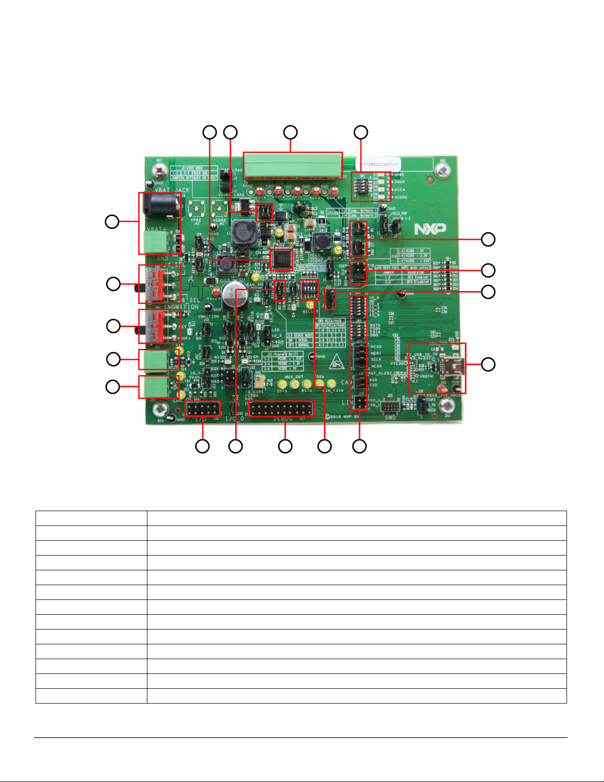
1
2
3
4
5
6
7
8
910
11
12
13
14
1516
1718
2.5 Board overview
The primary components of the evaluation boards are the onboard MCUs. The boards include an FS45xx or FS65xx and provide full
access to all the device’s features. An MKL25Z MCU USB controller enables access to the FS45xx/FS65xx through a USB connection.
In normal operation, configuration and monitoring applies to the on-board FS45xx/FS65xx device. However, the board can be totally
isolated from the on-board MCU. This allows connection to an off-board MCU without interference from the on-board device functions.
Table 3. Board description
Number Description
1V
2V
3 Ignition key — Ignition key from car
4 LIN bus — LIN bus connector
5 CAN bus — CAN bus connector
6 I/Os — Input and Output from FS45XX/FS65XX (IO0, IO2, IO3, IO4, IO5, GND, V
7 DBG mode select
8 Debug connector — Could be used for debug purpose (CAN TX/RX, LIN TX/RX, SPI, Debug, FS0B, FS1B, INTB)
9V
10 MCU to FS65/FS45 connection — Connects part or totality of signals between the KL25Z MCU and FS65XX/FS45XX.
11 KL25 MCU — Location of MCU and USB connector for control through FlexGUI
12 DFS mode select — Enables or disables the deep fail-safe function
Figure 3. Board description
connectors — Use either jack connector or Phoenix connector to supply board
BAT
switch — Select V
BAT
from jack or from Phoenix connector
BAT
CCA
& V
selection — Select 3.3 V/5.5 V configuration for V
AUX
CCA
& V
AUX
, VDDIO, V
KAM
BAT
)
Rev. 2
NXP Semiconductors 7
Page 8

Getting to know the hardware
Table 3. Board description (continued)
Number Description
13 V
14 Compensation network — Selects either Network 1 or 2
15 Power supplies LED — Visualizes regulator state (on or off). The switches can disconnect LEDs
16 Power supplies — Connector for power supplies (CAN_5V/V
17 Buck/buck or boost selection — These jumpers select V
18 FS45xx/FS65xx
CORE
selection — Selects either 1.23, 3.3, or 5.0 V on V
DC/DC
CORE
PRE/VCORE/VCCA/VAUX
mode as a buck or buck or boost.
PRE
)
Rev. 2
8 NXP Semiconductors
Page 9
2.6 LEDs
CAN_5
V
Vbat
FS1
b
FS0
b
RST
b
KEY
INT
b
Vpre
Vaux
Vcca
VCor
e
IO_
0
P3V3_KL2
5
Green LED Red LED
The LEDs are located on the board as shown in Figure 4.
Getting to know the hardware
Figure 4. LEDs
The LEDs can be switched on or off through jumpers or switches. Table 4 shows the function of all LEDs.
Table 4. LEDs
Schematic label Name Color LED activation Description
D1
D3
D4
D5
V
V
V
V
PRE
AUX
CCA
CORE
D10 IO_4 Green D10/J21-2/3 IO_4 high level
D11 KEY Green D11/J16 Ignition key switch to V
D13 RSTB Red D13/J25 RSTB asserted (logic level = 0)
D14 INTB Red D14/J28 INTB asserted (logic level = 0)
D15 P3V3_KL25 Green D15/NA MCU KL25 power supply ON
D17 CAN_5V Green D17/J27 CAN_5V ON
D18
D20 FS0B Red D20/J39 FS0B asserted (logic level = 0)
V
BAT
D21 FS1B Red D21/J40 FS1B asserted (logic level = 0)
Green D1/SW1-1 V
Green D3/SW1-2 V
Green D4/SW1-3 V
Green D5/SW1-4 V
Green D18/J28 V
PRE
AUX
CCA
CORE
BAT
on
on
on
on
SUP3
ON
(tied to IO_0)
Rev. 2
NXP Semiconductors 9
Page 10
Getting to know the hardware
SW3
SW6
SW5
Jumper
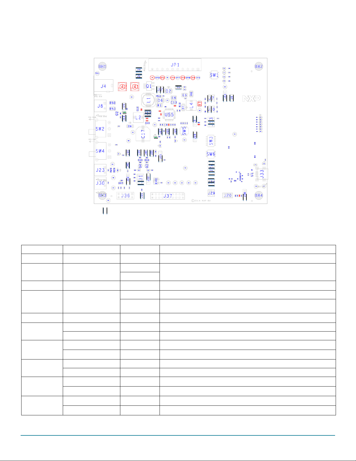
2.7 Jumper settings
Figure 5 shows the location of all jumpers on the board. Ta ble 5 provides the name and function of each jumper.
Figure 5. Jumpers
Table 5. Jumper settings
Schematic label Function Pin Number Jumper/pin function
load
JI
J2
J3
V
CORE
V
PRE
V
PRE
mode
load
J5 VDDIO selection
output capacitor
J6
J7
J9
J10
J11
J12
V
CORE
Comp. network1 1-2 Select compensation network1. Used in conjunction with J10:1-2
Comp. network2 3-4 Select compensation network2. Used in conjunction with J10:3-4
PNP
V
CCA
V
MOS
CCA
Comp. network1 1-2 Select compensation network1. Used in conjunction with J7:1-2
Comp. network2 3-4 Select compensation network2. Used in conjunction with J7:3-4
PNP
V
CCA
V
MOS
CCA
V
1-2
SUP
V
3
SUP
1-2 Connect 30 Ω resistor load on V
1-2
3-4
Both jumper plugged: V
PRE
Both jumper unplugged: V
1-2 Connect 60 Ω resistor load on V
1-2 VDDIO referenced to V
2-3
1-2 V
VDDIO referenced to V
or R107, respectively V
output capacitance. When set, adds 20 µF on V
CORE
CCA
CORE
CORE
Buck configuration
Boost configuration
PRE
PRE
or P3V3_KL25Z. Configuration is selected with R106
or P3V3_KL25Z
CORE
External PNP used Used in conjunction with J11:1-2
1-2 Internal MOS used Used in conjunction with J11:2-3
1-2 External PNP used in conjunction with J11:1-2
2-3 Internal MOS used in conjunction with J11:2-3
1-2 Connect V
3-4 Connect V
and V
SUP1
to the power supply (before PI filter)
SUP3
to the power supply on the output of PI filter
SUP2
CORE
.
Rev. 2
10 NXP Semiconductors
Page 11
Table 5. Jumper settings (continued)
Schematic label Function Pin Number Jumper/pin function
J13
J14
V
CORE
V
SENSE
setting
1-2 V
3-4 V
5-6 V
1-2 Connect V
CORE
CORE
CORE
= 1.23 V
= 3.3 V
= 5.0 V
SENSE
to V
BAT
J15 Debug mode 1-2 ON: Debug mode off: normal mode
J16 KEY LED 1-2 Enable KEY signaling LED
J18 DFS
J21 IO_4
1-2 DFS enabled
2-3 DFS disabled
1-2 IO_4 tied to GND through 510 k
2-3 IO_4wired on LED signaling works in conjunction with J19:1-2
IO_5 1-2 Connect IO_5 to KL25Z and I/O connector (J36-5)
J22
V
KAM
2-3 Connect V
to I/O connector(J36-8) and 220 nF capacitor.
KAM
J25 RSTB 1-2 Enable RSTB signaling LED
J26 INTB 1-2 Enable INTB signaling LED
J27 CAN_5V 1-2 Enable CAN_5V signaling LED
V
V
BAT
CORE
drift
1-2 Enable V
1-2 V
3-4 V
5-6 V
CORE
CORE
CORE
signaling LED
BAT
= 1.23 V
= 3.3 V
= 5.0 V
1-2 Connect FB_Core to FCRBM
2-3 Connect potentiometer R40 to FCRBM
J28
J31
J32 FCRBM
J35 IO-0 1-2 Connect IO_0 to ground through 510 k
J38 FS0B Pull-up
1-2 FS0b pull-up connected to VSUP3
2-3 FS0b pull-up connected to VDDIO
J39 FS0B LED 1-2 Enable FS0B signaling LED
J40 FS1B LED 1-2 Enable V
J41
J42
V
V
CORE
PRE
1 SMB connector on V
1 SMB connector on V
FS signaling LED (FS1B)
PU
CORE
PRE
J43 IO_5 1-2 Connect IO_5 to ground through 5.1 k
Getting to know the hardware
Rev. 2
NXP Semiconductors 11
Page 12

Getting to know the hardware
INTb
MUX_OUT
FS0b
FS1b
RSTb
CANL
CANH
LIN
GND
Vsup3
PGND
GND
Vpre
Vcore
Vaux
Vcca
CAN_5V
VSW_Pre
VSW_Core
GND
GND
P5V0_USB_VBUS
SELECT
FCRBM
GND
TC_USB_ID_TP
2.8 Test point definitions
Figure 6 shows the location of the test points on the board.
Figure 6. Test points
The following test points provide access to various signals to and from the board.
Table 6. Test points
Schematic label Signal name Schematic label/description
TP1 GND Ground
TP2 GND Ground
V
PRE
V
AUX
V
CCA
V
CORE
V
SUP3
TP3/V
TP7/V
TP9/V
TP11/V
TP16/V
regulator output voltage
PRE
output voltage
AUX
output voltage
CCA
output voltage
CORE
switcher signal
PRE
voltage
SUP3
TP3
TP4 GND Ground
TP5 CAN_5V TP5/CAN power supply
TP6 GND Ground
TP7
TP8 GND Ground
TP9
TP10 PGND TP10/power ground
TP11
TP12 GND Ground
TP13 GND Ground
TP14 PGND Power ground
TP15 VSW_PRE TP15/V
TP16
TP17 GND Ground
12 NXP Semiconductors
Rev. 2
Page 13

Table 6. Test points (continued)
Power Supply
Vbat
(Jack)
Vbat
(Phoenix)
CAN
LIN
I/Os Debug
USB
SWD
Schematic label Signal name Schematic label/description
TP18 VSW_Core TP18/V
TP19 SELECT TP19/SELECT pin voltage
TP20 TC_USB_ID_TP TP20/USB Identification pin
TP21 LIN TP21/LIN bus signal
TP22 GND Ground
TP23 FCRBM TP23/feedback core resistor bridge monitoring
TP24 CANH TP24/CAN high
TP25 CANL TP25/CAN low
TP26 MUX_OUT TP26/MUX_OUT signal
TP27 INTB TP27/INTB/interrupt pin level. Active low
TP28 RSTB TP28/Reset. Active low
TP29 FS1B TP29/fail-safe 1 signal. Active low
TP30 FS0B TP30/fail-safe 0 signal. Active low
TP31 GND Ground
TP32 P5V_USB_CONN_VBUS TP32/USB power supply level
TP33 GND Ground
core
switcher
Getting to know the hardware
2.9 Connectors
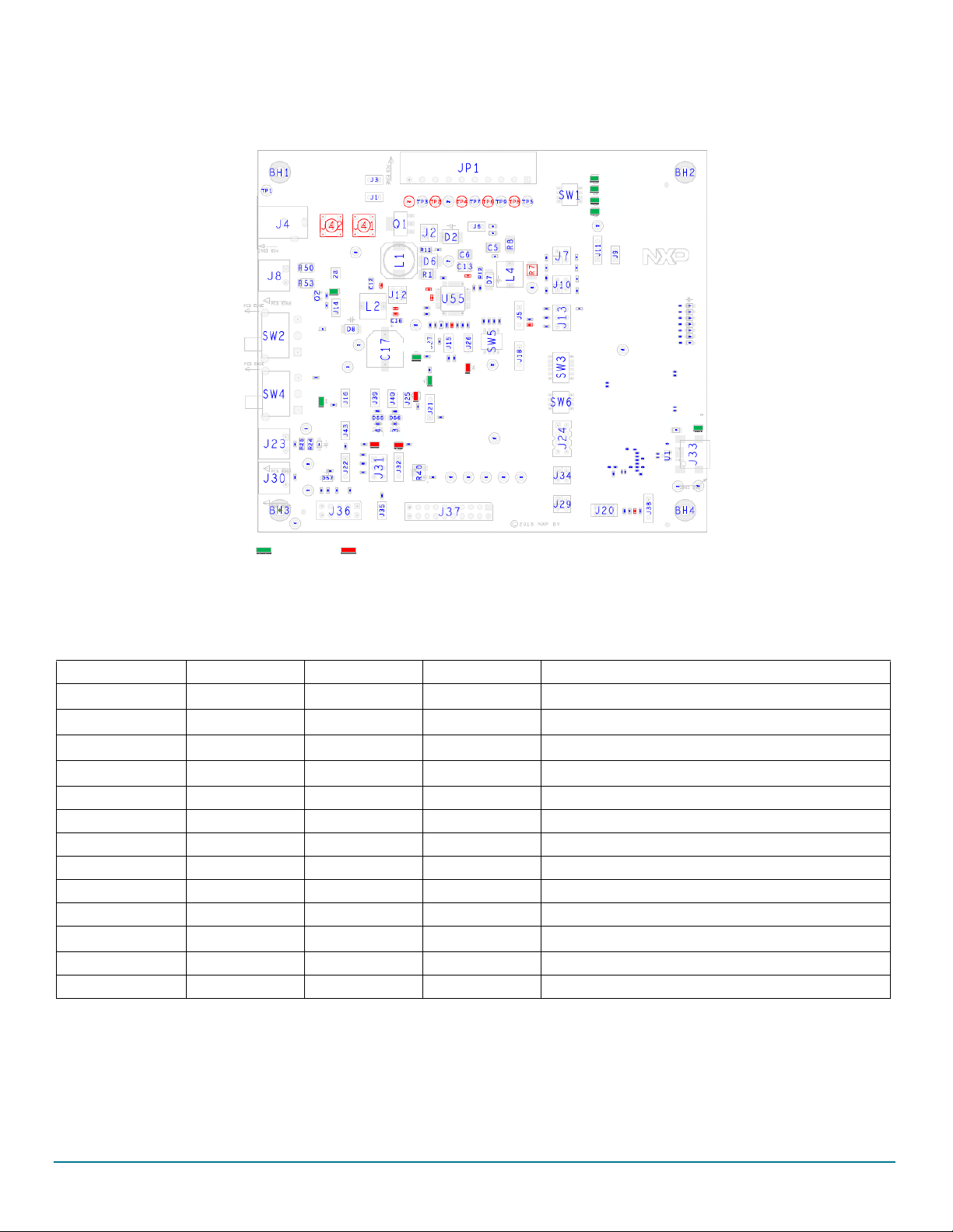
Figure 7 shows the location of connectors on the board. Table 7 and Tab l e 8 list the pin-outs for each connector.
Figure 7. Connectors
NXP Semiconductors 13
Rev. 2
Page 14

Getting to know the hardware
2.9.1 V
V
connects to the board either through jack connector (J4) or Phoenix connector (J8) at the user’s discretion. Switch SW2 switches
BAT
from one source to the other.
Table 7. V
Table 8. V
BAT
Pin number Connection Description
BAT
Pin number Connection Description
connectors (J4 and J8)
BAT
jack connector (J4)
1
2 Ground Connects to ground when switch SW2 is set to ground
Phoenix connector (J8)
1
2 Ground Connects to ground when switch SW2 is set to ground
V
BAT
V
BAT
Connects to V
Connects to V
when switch SW2 is set to V
BAT
when switch SW2 is set to V
BAT
BAT
BAT
2.9.2 Debug connector (J37)
The Debug connector (J37) gives access to the FS65xx main signal for debug or experimentation purposes.
Table 9. Debug connector (J37)
Pin number Connection Description
1 FSOB Fail-safe 0.
2 VDDIO Reference voltage for IOs.
3 MISO SPI, Master Input Slave Output
4 RSTB Reset, active low
5 MOSI SPI Master Output Slave Input
6 GND Ground
7 SCLK SPI serial clock
8 GND Ground
9 NCSB SPI chip select, active low.
10 GND Ground
11 MUX_OUT Multiplexer output
12 INTB Interrupt output. Active low.
13 RXD_L LIN receiver data. Logic level.
14 TXD_L LIN transmit data. Logic level.
15 GND Ground
16 FS1B Fail-safe 1
17 RXD CAN receiver data. Logic level
18 TXD CAN transmit data. Logic Level
19 DBG Debug pin selection
20 GND Ground
Rev. 2
14 NXP Semiconductors
Page 15

Getting to know the hardware
2.9.3 LIN connector (J23)
The LIN connector is mounted on all three kits, but LIN is supported only on the KITFS6522LAEEVM.
Table 10. LIN connector (J23)
Pin number Connection Description
1 LIN Connects to the LIN bus
2 GND Connects to ground.
2.9.4 CAN connector (J30)
Table 11. CAN connector (J30)
Pin number Connection Description
1 CANH Connects to the CANH bus line
2 CANL Connects to CANL bus line
2.9.5 USB connector (J33)
The USB connector provides a communication link between the evaluation board’s MKL25Z device and a PC running the FlexGUI software.
Table 12. USB connector (J33)
Pin number Connection Description
1 P5V0_USB_CONN_VBUS +5.0 V DC supply
2 USB_CONN_DN Data–
3 USB_CONN_DP Data+
4 TC_USB_ID_TP USB OTG ID
5 GND Ground
2.9.6 I/O connector (J36)
The I/O connector accesses the device under test (DUT) IO and V
Table 13. I/O connector (J36)
Pin number Connection Description
1 Not connected Not connected
2 IO_0 Input/Output 0
3 IO_3 Input/Output 3
4 IO_2 Input/Output 2
5 IO_5 Input/Output 5
6 IO_4 Input/Output 4
7 VDDIO Reference voltage for IOs.
8
9
10 GND Ground
V
V
KAM
BAT
signals.
KAM
Keep alive memory voltage
Battery voltage
Rev. 2
NXP Semiconductors 15
Page 16

Getting to know the hardware
SW3
SW6
SW5
Switches
ONOFF
2.9.7 Power supply connector (JP1)
The power supply connector (JP1) connects any of the SBC regulators to an external load or board for evaluation purposes.
Table 14. Power supply connector (JP1)
Pin number Connection Description
1 CAN_5V CAN voltage regulator
2 GND Ground
3
4 GND Ground
5
6 GND Ground
7
8 GND Ground
9
10 GND Ground
V
V
V
CORE
V
CCA
AUX
PRE
V
output voltage
CCA
V
auxiliary voltage regulator
AUX
V
voltage output
CORE
V
regulator output regulator
PRE
2.10 Switches
Figure 8. Switches
Rev. 2
16 NXP Semiconductors
Page 17

2.10.1 SW3
Table 15. SW3
Position Function Description
1 IO_O Connection between IO_O from product to MCU
2 NA Not used
3 IO_2 Connection between IO_2 from product to MCU
4 IO_3 Connection between IO_3 from product to MCU
5 IO_4 Connection between IO_4 from product to MCU
6 IO_5 Connection between IO_5 from product to MCU
2.10.2 SW5
Table 16. SW5
Switch V
1 – 8 3.3 V 3.3 V
2 – 7 5.0 V 5.0 V
3 – 6 3.3 V 5.0 V
4 – 5 5.0 V 3.3 V
CCA
V
AUX
Getting to know the hardware
2.10.3 SW6
Table 17. SW6
Position Function Description
1 RSTB Connection between RSTB from product to MCU
2 FS0B Connection between FS0B from product to MCU
3 FS1B Connection between FS1B from product to MCU
4 DBG Connection between DBG from product to MCU
Rev. 2
NXP Semiconductors 17
Page 18

Configuring the hardware
13.5 V Power Supply
+
USB
Port
J33
USB Cable
-
Connector
J4 or J8
KITFS4503CAEEVM/.,7)6&$((90
.,7)6/$((90 KITFS6522LAEEVM/KITFS6523CAEEVM
FS65XX / FS45XX
regulator output
External Load/Board
(Resistor Load or MCU power Supply)
PC with FlexGUI software installed
3 Configuring the hardware
3.1 Connecting the hardware
The KITFS4503CAEEVM / KITFS4508CAEEVM / KITFS6507LAEEVM / KITFS6522LAEEVM / KITFS6523CAEEVM must be connected
to a PC through the USB port on the board. A 13.5
The evaluation board connects to an external load or another board through connector JP1.
To avoid damaging the board, the V
1. With the power switched off, attach the DC power supply to either the Jack connector (J4) or the Phoenix connector (J8) on the
evaluation board. (There is no difference between the two connectors other than plug compatibility.)
2. Attach a load or an external board through connector JP1.
3. Connect a USB cable from the evaluation board USB port (J33) to the USB port on a PC with the FlexGUI installed.
4. Turn on the DC power supply.
Figure 9 illustrates the hardware configuration.
V power supply connects either to a jack connector (J4) or a Phoenix connector (J8).
Caution:
voltage must not exceed 40 V.
BAT
Figure 9. Evaluation board hardware configuration
Rev. 2
18 NXP Semiconductors
Page 19

4 Evaluation board settings
J18
1
2
3
R65 12K
R64 24K
SW 5
1
2
3
4
8
7
6
5
Vpre
R66 5.1K
GND
R63 51K
SELECT
Q50
PHPT60603PY
4
1523
VCCA_B
J9
1
2
V cca_E
Vcca
Vpre
J11
1
2
3
C53
4.7uF
V cca [4]
GND
Evaluation board settings
4.1 V
To select various voltage levels on V
Table 18. SW5 V
Switch V
CCA
CCA/VAUX
and V
AUX
CCA
voltage configurations
CCA
setting
and V
AUX
, set the switch SW5 as shown in Table 18 and Figure 10 below:
V
AUX
1 – 8 3.3 V 3.3 V
2 – 7 5.0 V 5.0 V
3 – 6 3.3 V 5.0 V
4 – 5 5.0 V 3.3 V
Figure 10. V
V
regulator can be configured to use the internal PMOS transistor at current levels up to 100 mA. To achieve higher current levels (up
CCA
to 300 mA), use a PNP external transistor.
Table 19. J9/J11 V
PNP configurations
CCA
Ta bl e 19 and Figure 11 show the jumper settings for both configurations.
CCA
and V
voltage settings
AUX
Jumper J9 J11
Internal MOS OFF 2 – 3
External PNP ON 1 – 2
The V
CCA
NXP Semiconductors 19
regulator is always tied to the external PNP transistor. Resistors R105 and R10 limit the power dissipation in the PNP transistor.
Figure 11. V
Rev. 2
transistor setting
CCA
Page 20

Evaluation board settings
Q51
PHPT60603PY
4
1523
Va ux
Vaux_B
Vaux_E
C56
4.7uF
Vaux [4 ]
GN D
R109 2.4
R105 for Vau x = 5V
R109 for Vau x = 3.3V
R105 0
C1
10uF
J13
1 2
3 4
65
C5
22uF
Vcore
C2
10uF
R58 43K
R51
15
R52
15
D7
PMEG3030BEP
A C
PGND
5 - 6 Vcore = 5.0V
3 - 4
1 - 2
Comp. Network 1
J7/J10
Comp. Network 2
GND
VSW_C ore
R12
15
FB _C ore
Pr od uc t wi th V co re D C/ DC o nl y (F S6 5X X)
Pr od uc t wi th V co re L DO o nl y (F S4 5X X)
R57
39K
C7 150pF
R8 0
C3
680P F
J6
1
2
J1
HDR 1X2
1
2
1 - 2
3 - 4
Vcore [4]
Vcore = 3.3V
Vcore = 1.23V
Boost_core
PGN D
PGN D
PGN D
C19
0.1UF
L4 2.2uH
1 2
R15 4.32K
R9
8.06K
R10
200
R13 24.9K
C15
180PF
C52 1000PF
R6
510
C4
220PF
R56
18K
C9
10nF J7
123
4
J10
1 2
3 4
Com p_core
R7 0
DN P
FB _C ore
J13
PGN D
Vcore
Figure 12. V
4.2 V
4.2.1 V
CORE
CORE
The FS45xx family of devices only support V
voltage regulators. The evaluation board circuitry accommodates this discrepancy by implementing a separate circuit network for each of
settings and related configurations
and F45xx versus FS65xx
LDO (low dropout) voltage regulators. The FS65xx family only supports V
CORE
external transistor
AUX
CORE
DC/DC
the two device families. Populating or not populating resistors R7 and R8 depend on which device family is in use and determines which
network is enabled.
For the FS45xx family, R7 is populated and R8 is not populated. For the FS65xx family, R8 is populated and R7 is not populated. Because
resistor R8 is not populated for FS45xx devices, the compensation network is also disabled for those devices. See
Figure 13.
20 NXP Semiconductors
Figure 13. V
Rev. 2
configuration
CORE
Page 21

4.2.2 Compensation network
R32 4.32K
R33 24.9K
R4 0
5. 0 K
1 3
2
R4 2
5. 6 K
J3 1
1 2
3 4
65
J32
1
2
3
1 - 2 Vc ore = 1 .23V
3 - 4 Vc ore = 3 .3V
J31
VcoreFB Drift
5 - 6 Vc ore = 5 V
Vcore
R6 0 43 K
FCRB M
FB_Core
GND
Evaluation board settings
Both LDO and DC/DC voltage regulators use V
bridges enable feedback support for either FS45xx or FS65xx devices (see
voltage feedback to control the output voltage. For this reason, two separate external
CORE
Figure 13).
For FS45xx devices using static (steady-state) LDO regulators, a simple resistor bridge (resistors R15/R13/R58 and R9) in conjunction
with jumper settings on jumper J13 determines the feedback voltage.
For FS65xx devices using DC/DC voltage regulators, a selectable pair of RC voltage dividers control the dynamic behavior of the regulator.
One RC divider --compensation network 1-- consists of the resistor-capacitor series R10/C4/R57/C52. The other RC divider
--compensation network 2-- consists of the resistor-capacitor series R6/C3/R56/C7. Jumpers J7 and J10 select which of the two
compensation networks is enabled.
The default value for compensation network 1 is 1.23 V. For compensation network 2, the default value is 3.3 V. These values can be
changed for other configurations. The compensation network tool referenced in
Ta bl e 26 is useful in calculating the appropriate values.
Table 20 illustrates the jumper settings for each feedback voltage level.
Table 20. V
Notes
1. Use compensation network tool to calculate value
compensation network settings
CORE
Jumper setting
Static behavior Dynamic behavior
V
CORE
J13J7J10
1.23 V 1–2 1–2 1–2
3.3 V 3–4 3–4 3–4
5.0 V 5–6 (1) (1)
4.2.3 FCRBM resistor bridge
The feedback core bridge monitoring (FCRBM) resistor bridge is an evaluation board safety feature.
The bridge generates the same voltage as the bridge connected to the FB_core pin. If the difference between the two voltages is greater
than the VCORE_FB_DRIFT value, the FS state machine is impacted (refer to data sheet).
To implement this functionality, use jumper J31 to configure the second resistor bridge as shown in Figure 14. Then, set the potentiometer
R40 to match the voltage of the first V
To disable the FCRBM function, place a jumper on position 1–2 of J32. This connects FB_CORE directly to the FCRBM bridge, causing
the drift to be zero.
bridge.
CORE
Figure 14. FCRBM bridge resistor
Rev. 2
NXP Semiconductors 21
Page 22

Evaluation board settings
J29
HDR 2X2
1 2
3 4
RXD _L_SH
J24
HD R_2 X4
1 2
3 4
65
7 8
TXD_ L_SW
MISO[3]
MOSI[3]
NCSb[3]
SCLK[3]
J34
HDR 2X2
1 2
3 4
RXD_S H
TXD_ MCU
CAN
RXD[3]
TXD _L[3]
TXD[3]
SP I
N CSb_MCU
SC LK_MCU
MOSI_MCU
MI SO _SH
RXD_L[3]
LIN
4.3 MCU settings
4.3.1 MCU jumper configuration
Table 21. MCU Jumper configuration
Schematic label Pin number Function Jumper/pin function
J24
J29
J34
1–2
3–4 Connect MOSI to KL25Z
5–6 Connect MSCLK to KL25Z
SPI
7–8 Connect NCSB to KL25Z
1–2
3–4 Connect TXD_L LIN to KL25Z
1–2
3–4 Connect RXD CAN to KL25Z
LIN
CAN
Connect MISO to KL25Z
Connect RXD_L LIN to KL25Z
Connect RXD CAN to KL25Z
Figure 15. MCU jumper configuration
4.3.2 MCU switch configuration
4.3.2.1 Switch SW3
Table 22. Switch SW3
Position Function Description
1 IO_O Connection between IO_O from product to MCU
2 NA Not used
3 IO_2 Connection between IO_2 from product to MCU
4 IO_3 Connection between IO_3 from product to MCU
5 IO_4 Connection between IO_4 from product to MCU
6 IO_5 Connection between IO_5 from product to MCU
22 NXP Semiconductors
Rev. 2
Page 23

Figure 16. Switch SW3
IO_4[3]
IO_5[3]
IO_0[3]
IO_2[3]
IO_3[3]
SW 3
SW _D I P- 6_S M
1
2
3
4
5
6
12
11
10
9
8
7
IO_SW_2
IO_SW_0
IO_SW_5
IO_SW_4
IO_SW_3
SW 6
SW D I P-4/ S M
1
2
3
4
8
7
6
5
RSTb[3]
FS0b[3]
FS1b[3]
DBG[3]
DBG_SW
FS1b_SW
FS0b_SW
RSTb_SW
4.3.2.2 Switch SW6
Table 23. Switch SW6
Position Function Description
1 RSTB Connection between RSTB from product to MCU
2 FS0B Connection between FS0B from product to MCU
3 FS1B Connection between FS1B from product to MCU
4 DBG Connection between DBG from product to MCU
Evaluation board settings
Figure 17. Switch SW6
4.3.3 MCU analog input
To assure the complete isolation of analog signals connected from an external component to the MCU, remove input resistance as
applicable for the following:
•V
•V
•V
•V
• CAN_5V tied to MCU through R80
• MUX_OUT tied to MCU through R71
•V
•V
tied to MCU through R82
PRE
tied to MCU through R89
CORE
tied to MCU through R90
AUX
tied to MCU through R82
CCA
tied to MCU through R70
DDIO
tied to MCU through R79
KAM
NXP Semiconductors 23
Rev. 2
Page 24

Software
MKL25Z
Pre-loaded
firmware
KITxxx evaluation board
FS45xx/FS65xx
FlexGUI
x
Windows Laptop
FSxxxx.xml
MyRegs.xls
USB
5 Software
The KITFS4503CAEEVM / KITFS4508CAEEVM / KITFS6507LAEEVM / KITFS6522LAEEVM / KITFS6523CAEEVM is bundled with
software allowing the user to interact directly with the onboard MCU during the development process. The boards contain an MKL25Z
Kinetis processor pre-loaded with firmware controlling communication with the FS45xx/FS65xx MCU. A graphical user interface installed
on a PC serves as the user interface to the evaluation board. When connecting the evaluation board to a PC through a USB cable, the
following data exchanges are available:
• SPI access (read and write) to FS45xx/FS65xx
• ADC readout, connected to regulators
–V
PRE
–V
CORE
–V
AUX
–V
CCA
– CAN_5V
– MUX_OUT
–V
DDIO
–V
• I/O readout, connected to IO_0 to IO_5
• FS0B/FS1B readout
• RSTB readout
• CAN generated TX signal
• LIN generated TX signal with loopback checking
Note that MCU connections to FS45XX/FS65XX can be fully isolated by removing related jumpers and switching off the related switch.
The software bundle also includes an XML file containing register descriptions for the FS45xx or FS65XX (depending on the evaluation
board). This file must be installed for the GUI to work properly. In addition, an optional Excel file can be created to facilitate setting several
registers at a click.
KAM
FS45xx/FS65x
Figure 18. Software overview
5.1 Installing the FlexGUI
The FlexGUI graphical user interface provides a PC-based interface for accessing the evaluation board and exercising FS45xx/FS65xx
functions. The GUI runs on any Windows 8, Windows 7, Vista, or XP-based operating system.
To install the FlexGUI software:
1. Go to the evaluation board tool summary page
2. Under Jump Start Your Design, click on the Get Started with the KITFS65xx link.
3. From the list of files that appear, click on the FlexGUI link. The software downloads to the PC and initiates the installation. An
installation wizard guides the user through the process. Upon completion, the GUI executable (FlexGUI.exe), and the relevant
register description XML file are installed on the system.
4. To simplify launching the FlexGUI, create a .bat file with the following commands:
C:\Program Files (x86)\FlexGUI\bin\FlexGUI.exe
24 NXP Semiconductors
Rev. 2
Page 25

Software
Mandatory Optional
C:\Program Files (x86)\FlexGUI\Sequences&Config\FSxxxx.xml
5.2 Creating and using a register configuration file
Creating an Excel register configuration file allows the user to initialize the evaluation board MCU with a predefined set of register values.
To create a register configuration file, do the following:
1. Open a new Excel spreadsheet file and label the first three columns in row 1 hex, registers and comment. Notice that the first two
columns —hex and registers— are mandatory. The comment column is optional.
2. In the hex column (column A), enter the data or address to be assigned to each register. The address and data must be contained in
two bytes and must be expressed as a hexadecimal value. Enter one row per register.
3. In the registers column (column B), enter the register name associated with the value in the hex column.
4. In the comments column (column C), enter any comments desired. Data in this column is not processed by the FlexGUI.
Figure 19 illustrates a typical register configuration file.
Figure 19. Register configuration Excel file
5. Launch FlexGUI. When FlexGUI opens, click the load sequence button to load the register configuration file (see Figure 20).
Rev. 2
NXP Semiconductors 25
Page 26

Software
12
Figure 20. Loading the register configuration example file
6. Send the resister configuration file to the FS45xx/FS65xx by clicking the send sequence button (see Figure 20).
5.3 Using the FlexGUI
To start the FlexGUI, do the following:
1. Configure the hardware as described in Section 3.1, Connecting the hardware.
2. To launch the FlexGUI, execute the .bat file created in Section 5.1, Installing the FlexGUI.
5.4 Use case example
This example assumes the user has configured the hardware as shown in Figure 9 and put the evaluation board into debug mode by
placing a connector on jumper J15 (see Table 5). After launching the FlexGUI, the example configures registers to disable IO_23_FS
safety mode, disable the watchdog and release the FSx pins.
1. Create an Excel file configured as shown in Ta bl e 24. For details on creating an Excel register configuration file, see Section 5.2,
Creating and using a register configuration file.
Table 24. Use case register configuration Excel file example
HEX Registers Comment
C424 BIST ABIST2_VAUX enabled => Start V
CB0C INIT_FSSM IO_23_FS Disabled
8900 INIT_INT Close main machine initialization sequence
D34D WD_refresh_0 1st Watchdog refresh answer
D29B WD_refresh_1 2nd Watchdog refresh answer
D237 WD_refresh_2 3rd Watchdog refresh answer
D26E WD_refresh_3 4th Watchdog refresh answer
D2DC WD_refresh_4 5th Watchdog refresh answer
D2B9 WD_refresh_5 6th Watchdog refresh answer
AUX
ABIST
Rev. 2
26 NXP Semiconductors
Page 27

Software
Table 24. Use case register configuration Excel file example (continued)
HEX Registers Comment
D372 WD_refresh_6 7th Watchdog refresh answer
D4A7 RELEASE_FSxB Release FS0B & FS1B pins
2. To use the register configuration file, open FlexGUI, then load the register configuration file and send it to the evaluation board (see
Figure 20).
Now read or write any bit from the FS45xx/FS65xx on-board MCU as shown in Ta bl e 21.
Figure 21. FlexGUI register window
Register values display in the register value window as shown in Figure 22.
Figure 22. FlexGUI register value window
Rev. 2
NXP Semiconductors 27
Page 28

Schematic
5
5
4
4
3
3
2
2
1
1
D D
C C
B B
A A
Vcca Vaux
J18
DEEP FAIL SAFE mode select
Jumper Regulator
DFS Disabled
DFS Enabled1-2
CAN
LIN
Power Supply
DEBUG
SW5
Vcca/Vaux Voltages config.
SWITCH
5 3.3
1-8
2-7
3-6
4-5
3.3 5553.3 3.3
Vcca
2-3
Populated on product
with LIN Option only
Vbat
Vcore_sense
ON
OFF
J15-DEBUG MODE
DEBUG
NORMAL
1 - 2
3 - 4
Vcore = 1.23V
Vcore = 3.3V
J31
VcoreFB Drift
5 - 6 Vcore = 5V
Contact KEY
Vsup3
1;3
Vsup12
J2-Vpre mode
1-2 & 3-4
Jumpers off Buck or Boost
Buck only
Vbat Jack
Product with Vcore DC/DC only
Product with Vcore LDO only
1 - 2
3 - 4
Vcore = 1.23V
Vcore = 3.3V
J13
Vcore
Test Points
I/O
LED Signalling
INGNITION
5 - 6 Vcore = 5.0V
1 - 2
3 - 4
Comp. Network 1
J7/J10
Comp. Network 2
Vaux
J11
J9 / J11
Vcca PNP Config.
Jumper
Int MOS
Ext PNP 1-2ON
OFF 2-3
J9
LIN Product :
- R29 : Populated
- R98 / R108 / C24 DNP
- R69 : DNP
- R17 : Populated
FS1b Products :
- R29 : DNP.
- R98 / R108 / C24 : Populated
- R69 : Populated
- R17 : DNP
R105 for Vaux = 5V
R109 for Vaux = 3.3V
D57 & C93 as close
as possible to the IC
J5 - VDDIO Voltage Selection
FS0b
Vaux_B
Vaux_E
Vcca_E
CANH
SELECT
LIN
MUX_OUT
DBG
MISO
SCLK
INTb
FS1b
VCCA_B
FS0_b
MOSI
NCSb
RXD_L
RXD
RSTb
TXD_L
TXD
VSW_Pre
FS0_b
TXD
FCRBM
FS_PU
INTb
KEY
IO_0
Vsense
Vsup
Vsense
DBG
CANH
CANL
Vkam_IO5
VCCA
VCCA_B
VCCA_E
VAUX_E
VAUX_B
VAUX
RXD
TXDL_VpuFS1b
FB_Core
Boost_core
Comp_core
FB_Core
INTb
VSW_Core
FCRBM
SELECT
CANH
CANL
LIN
FS0b
MUX_OUT
RSTb
VSW_Pre
IO_0
IO_4
IO_3 IO_5
RSTb
INTb
IO_4
Vkam_IO5
FS1b
FS_PU TXDL_VpuFS1b
IO_2
FCRBM
FB_Core
IO_5
LIN
FS1b
FB_core
Boost_core
VSW_Core
Comp_core
SELECT
VSW_Core
CANL
Vkam
PGND
PGND
PGND
PGND
PGND
PGND
PGNDPGND
PGND
PGND
PGND
PGND
PGND
PGND
PGND
PGND
PGND
PGND
PGND
PGND
PGND
PGND
PGND
PGND PGND
Vsup3
Vsup3
Vbat
Vsup3
Vcore
CAN_5V
Vpre
Vsup3
VDDIO
Vcca VDDIOVcore P3V3_KL25Z
VDDIO
Vcore
CAN_5V
CAN_5V
CAN_5V
Vpre
Vpre
Vcca
Vaux
Vcore
KEY
Vaux VpreVccaVcore
Vaux
Vaux
Vpre
Vcca
CAN_5V Vsup3
Vcore
Vbat
VDDIO
VDDIO
Vbat
Vcca
Vcore
VDDIO
VDDIO
VDDIO
Vpre
Vpre
Vpre
Vpre
Vpre
GND
GND
GND
GND
GND
GND
GND
GND
GND
GND
GND
GND
GND
GND
GND
GND
GND
GND GND GND GND
GND GND
GND
GND
GND
GND GND
GND
GND GND
GND
GND
GND
GND
GND
GND
GND
GND
GND
GND
GND
GND
GND GND
GND
GND
GND
GND
GND
GND
GND
GND
GND
GND
GND GND
GND
GND
GND
GND
Vpre
GND
Vcca [4]
Vaux [4]
MOSI [4]
MISO [4]
SCLK [4]
NCSb [4]
IO_0[4]
IO_4[4]
IO_2 [4]
IO_3 [4]
FS0b[4]
Vpre [4]
Vddio
[4]
CAN_5V [4]
RXD_L[4]
Vcore[4]
RSTb
[4]
Vkam[4]
DBG [4]
RXD[4]
TXD[4]
TXD_L[4]
IO_5 [4]
FS1b[3,4]
FS1b [3,4]
MUX_OUT [4]
Drawing Title:
Size Document Number Rev
Date: Sheet
of
Page Title:
ICAP Classification: CP: IUO: PU BI:
SCH-29225 PDF: SPF-29225
A
KITFS6522LAEEVM
C
Wednesday, April 06, 2016
FS6500
34
___ ___
X
Drawing Title:
Size Document Number Rev
Date: Sheet of
Page Title:
ICAP Classification: CP: IUO: PU BI:
SCH-29225 PDF: SPF-29225
A
KITFS6522LAEEVM
C
Wednesday, April 06, 2016
FS6500
34
___ ___
X
Drawing Title:
Size Document Number Rev
Date: Sheet of
Page Title:
ICAP Classification: CP: IUO: PU BI:
SCH-29225 PDF: SPF-29225
A
KITFS6522LAEEVM
C
Wednesday, April 06, 2016
FS6500
34
___ ___
X
C20
1000PF
R81
11.0K
TP25
SW2
123
S1
S2
TP12
J15
1
2
R60 43K
R102
510K
Q2
NX3008NBK
1
2 3
TP17
C16 4.7uF
C55
10nF
DNP
J39
1
2
R23
510K
C63
1000PF
DNP
R97
510K
J12
12
34
R43
510K
L3
MPZ1608S101A
1 2
Q1
BUK9832-55A
1
3 2
4
TP5
C59
10nF
DNP
C52 1000PF
R101
5.6K
SW1
123
4
876
5
R107
0
DNP
BH3
MTG1
J22
1
2
3
TP18TP31
SW4
500SSP3S1M6QEA
123
S1
S2
R2 1.5K
J13
1 2
3 4
65
Q51
PHPT60603PY
4
15
2
3
D11 LED/GRN
A C
C3
680PF
R94
5.1K
R93
10K
TP4
DNP
1
R105 0
R8 0
TP2
DNP
1
C91
0.47UF
R30
1.5K
R7 0
DNP
1
J41
DNP
TP21
R29 0
C12 4.7uF
R36
120
R6
510
J32
123
R106 0
R17 0
R55
30
R76 5.1K
D56
BZT52H-B18
A C
R57
39K
TP16
R69 0
DNP
C51
0.22uF
R66 5.1K
C21
2.2UF
D2
SS24T3G
A C
L4 2.2uH
1 2
R108
16.2K
R109 2.4
TP26
J10
1 2
3 4
R95 5.1K
R51
15
J6
1
2
1
J42
DNP
C5
22uF
C18
0.1UF
C6
22uF
R96
10K
D12 1N4148WS
AC
BH1
MTG1
R58 43K
+
C17 47uF
BH2
MTG1
R28 0
J3
HDR 1X2
1
2
J9
1
2
TP3
TP30
J23
PLUG_1X2
1
2
J31
1 2
3 4
65
C7 150pF
C50
0.1UF
D57
BZT52H-C20
A C
D4 LED/GRN
A C
C4
220PF
R98 10K
DNP
R15 4.32K
R19
1.5K
J40
1
2
R110
510K
TP23
R103
10K
L2
1uH
1 2
R52
15
Q3
BSS84LT1
1
3 2
R104 5.1K
C26
10nF
DNP
TP28
D17 LED/GRN
A C
TP13
J43
1
2
J8
1
2
C13
22uF
J36
1 2
3 4657 8
9 10
C57
1uF
R3 560
C54 10nF
DNP
C11 10nF
DNP
D13
RED
AC
C28
10nF
J28
1
2
TP29
R37 560
R4 560
C10 10nF
DNP
D8
PMEG10030ELP
AC
R14 10K
R56
18K
TP27
R24
2K
J16
1
2
J11
123
R9
8.06K
D1 LED/GRN
A C
C29
1000PF
TP6
DNP
1
U55
MC33FS6522LAE
CAN_5V7CANH8IO_5/VKAM11IO_410GND_COM6CANL9IO_0
12
LIN5VSUP11VSUP22VSENSE3VSUP3
4
FCRBM
13
FS0
14
DEBUG
15
AGND
16
MUX_OUT
17
IO_2
18
IO_3
19
TXD
20
RXD
21
TXDL
22
RXDL
23
RST
24
MISO25MOSI
26
SCLK
27
CS
28
INT
29
VDDIO
30
SELECT
31
FB_CORE
32
COMP_CORE
33
VCORE_SNS
34
SW_CORE
35
BOOT_CORE
36
VPRE
37
VAUX
38
VAUX_B
39
VAUX_E
40
VCCA_E
41
VCCA_B
42
VCCA
43
GATE_LS
44
DGND
45
BOOT_PRE
46
SW_PRE2
47
SW_PRE1
48
EP
49
R22
510K
R1 0
C25
0.22UF
TP19
R75 5.1K
R40
5.0K
1 3
2
TP8
DNP
1
J18
123
R100
5.6K
J25
1
2
R27 5.1K
J30
PLUG_1X2
1
2
C56
4.7uF
R63 51K
TP22
J37
1 2
3 4657 8
9 10
11 12
13 14
15 16
17 18
19 20
TP15
JP1
PLUG_1X10
123456789
10
R25
2K
C27
10nF
C53
4.7uF
J2
1
2
3
4
C14
10nF
DNP
R65 12K
D14
RED
AC
J5
123
D21
RED
AC
C9
10nF
TP11
J14
1
2
C8
470PF
R10
200
D18 LED/GRN
A C
J27
1
2
R32 4.32K
TP7
C15
180PF
R42
5.6K
R53 0
C1
10uF
J38
1
2
3
D20
RED
AC
D5 LED/GRN
A C
R26
5.1K
R5 1.5K
D6
SS24T3G
A C
R20 1.2K
R16
5.1K
J21
1
2
3
D10
LED/GRN
AC
D7
PMEG3030BEP
A C
C58
10nF
DNP
Q4
BSS84LT1
1
3 2
TP14
TP24
Q50
PHPT60603PY
4
15
2
3
C93
0.47UF
C2
10uF
TP10
DNP
1
R11
15
C24
3.3uF
C19
0.1UF
C92
10nF
DNP
J26
1
2
C66
10nF
R50 0
L1 22UH
12
Q53
NX3008NBK
1
2 3
R54
30
R13 24.9K
SW5
123
4
876
5
R74 5.1K
TP9
R39 1.2K
R99
10K
J1
HDR 1X2
1
2
R33 24.9K
J7
1
2
3
4
R12
15
R111 0
TP1
BH4
MTG1
J4
123
R31
1.5K
R64 24K
J35
1
2
D55
BZT52H-B18
A C
D3
LED/GRN
A C
C69
1000PF
28 NXP Semiconductors
6 Schematic
Figure 23. Evaluation board schematic
Rev. 2
Page 29

5
5
4
4
3
3
2
2
1
1
D D
C C
B B
A A
&$'127(
3OHDVHSODFHWKHVHFDSDFLWRUV
QHDUWKHLUUHVSHFWLYH&38SLQ
95()+WR95()/
DQG9''$WR966$
'HFRXSOLQJFDSDFLWRUV
VKDOOEHXVHGIRUWKHVH
SLQV9''9''9''$
Analog Inputs
Digital IOs
HIGH_to_LOW
Level Shifter
./=86%&211(&725
6:'&211(&725
&$'127(
3OHDVHSODFH39B./=
FDSDFLWRUFORVHWRWKH
9287SLQ
./='HFRXSOLQJ&DSV
63,
/,1
,2V
6SHFLDO,2V
&$1
FAST HIGH_to_LOW
Level Shifter
VREFH
AN_IN_1
AN_IN_2
AN_IN_3
AN_IN_4
AN_IN_5
AN_IN_6
AN_IN_7
GPIO_0
GPIO_1
GPIO_2
GPIO_3
GPIO_4IO_SW_0
IO_SW_2
IO_SW_3
IO_SW_4
IO_SW_5
RXD_L_MCU
RXD_L_MCU
TXD_L_MCU
TC_USB_ID_TP
SHIELD_K20USB
USB_CONN_DN
USB_CONN_DP
P5V0_USB_CONN_VBUS
USB_DM
USB_DP
USB_DM
USB_DP
SWD_DIO
SWD_CLK
RST_KL25Z
GPIO_0
GPIO_1
GPIO_2
GPIO_3
GPIO_4
GPIO_5
GPIO_6
GPIO_7
GPIO_8
MISO_MCU
MOSI_MCU
SCLK_MCU
IO_SW_0
IO_SW_2
IO_SW_3
IO_SW_4
IO_SW_5
RSTb_SW
FS0b_SW
FS1b_SW
FS0b_SW
FS1b_SW
RSTb_SW
GPIO_6
GPIO_7
GPIO_8
MOSI_MCU
SCLK_MCU
NCSb_MCU
MISO_SH
RXD_L_SH
RXD_L_SH
SWD_CLK
SWD_DIO
NCSb_MCU
TXD_MCU
RXD_SH
RXD_SH RXD_MCU
TXD_MCU
RXD_MCU
AN_IN_0
PTE29
TXD_L_MCU
TXD_L_SW
TXD_L_SW
GPIO_5DBG_SW
DBG_SW
AN_IN_0
AN_IN_1
AN_IN_2
AN_IN_3
AN_IN_4
AN_IN_5
AN_IN_6
AN_IN_7
MISO_SH MISO_MC U
RST_KL25Z
GND
GND
GND
GND
GND
GND
GND
GND
GND
GND
GND
GND
GND
GND
GND
GND
GND
GND
GND
GND
GNDGNDGND GND
GND
GND
GND
GND
GND
GND
GND
GND
GND
GND
GND
GND
GND
GNDGND
GND
P3V3_KL25Z
P3V3_KL25Z
P3V3_KL25Z
P3V3_KL25Z
P3V3_KL25Z
P3V3_KL25Z
P3V3_KL25Z
P3V3_KL25Z
P3V3_KL25Z
P3V3_KL25Z
P3V3_KL25Z
P5V_KL25Z
P3V3_KL25Z
P3V3_KL25Z
P3V3_KL25Z
P3V3_KL25Z
P5V_KL25Z
VDDIO
MUX_OUT[3]
RSTb[3]
FS0b[3]
FS1b[3]
Vcore[3]
Vaux[3]
Vcca[3]
CAN_5V[3]
Vpre[3]
MISO[3]
MOSI[3]
NCSb[3]
SCLK[3]
IO_4[3]
IO_5[3]
IO_0[3]
IO_2[3]
IO_3[3]
Vkam[3]
RXD_L[3]
RXD[3]
DBG[3]
TXD_L[3]
TXD[3]
Vddio[3,4]
Vddio[3,4]
Drawing Title:
Size Document Number Rev
Date: Sheet
of
Page Title:
ICAP Classification: CP: IUO: PUBI:
SCH-29225 PDF: SPF-29225
A
KITFS6522LAEEVM
C
Wednesday, April 06, 2016
INTERFACE
44
___ ___
X
Drawing Title:
Size Document Number Rev
Date: Sheet of
Page Title:
ICAP Classification: CP: IUO: PUBI:
SCH-29225 PDF: SPF-29225
A
KITFS6522LAEEVM
C
Wednesday, April 06, 2016
INTERFACE
44
___ ___
X
Drawing Title:
Size Document Number Rev
Date: Sheet of
Page Title:
ICAP Classification: CP: IUO: PUBI:
SCH-29225 PDF: SPF-29225
A
KITFS6522LAEEVM
C
Wednesday, April 06, 2016
INTERFACE
44
___ ___
X
D53
PDZ36B
A C
U52
SN74LVC1T45
VCCA
1
GND2A
3
B
4
DIR
5
VCCB
6
R59 10K
-
+
U53B
MCP6004-I/SL
5
6
7
C82
1.0UF
C31
2.2UF
R21 10K
C60
0.1UF
C85
1.0UF
D54
PDZ36B
A C
R87
10K
C64
0.1UF
C77
0.1UF
C75
1.0UF
R92 0
D51
PDZ36B
A C
C65
0.1UF
D52
PDZ36B
A C
D50
PDZ36B
A C
SW3
SW_DIP-6_SM
12345
6
12111098
7
J20
HDR 2X5
1 2
3 4657 8
9 10
C80
0.1UF
C68
1.0UF
SW6
SW DIP-4/SM
123
4
876
5
R70
9.09k
C32
0.1UF
C90
0.1UF
5VD-D+IDG
CONN USB MINI-B
J33
123
4S25
S1
S3S4
J34
HDR 2X2
1 2
3 4
R61 10K
R41 33
R85
11K
-
+
U50B
MCP6004-I/SL
5
6
7
-
+
U53C
MCP6004-I/SL
10
9
8
TP56
TP55
R86
11K
C76
1.0UF
R90
9.09k
F50
MFU0805FF00500P100
1 2
R73
11K
R91 1.0M
DNP
R80
9.09k
C74
0.1UF
TP32
C73
0.1UF
C67
0.1UF
C72
0.1UF
R34 10K
C89
0.1UF
C83
0.1UF
R38 33
R62 10K
D16
PDZ36B
A C
D9
PDZ36B
A C
-
+
U50C
MCP6004-I/SL
10
9
8
R35
560
-
+
U53D
MCP6004-I/SL
12
13
14
TP57
TP54
C88
1.0UF
74HC4050D
U51
1A32A53A74A95A116A
14
1Y22Y43Y64Y105Y
12
NC_13
13
6Y
15
NC_16
16
VCC
1
GND
8
TP52
C78
0.1UF
C87
1.0UF
C30
0.1UF
MKL25Z128VFT4
U54
PTE20/ADC0_DP0/ADC0_SE0/T PM1_CH0/UART0_TX7PTE21/ADC0_DM0/ADC0_SE4A/TPM1_ CH1/UART0_RX8PTE30/DAC0_OUT/ADC0_SE23/CMP0_IN4/TPM0_CH3/TPM_CLKIN1
14
PTC4/LLWU_P8/SPI0_PCS0/UART 1_TX/TPM0_CH3
37
PTC5/LLWU_P9/SPI0_SCK/LPTMR 0_ALT2/CMP0_OUT
38
PTC6/LLWU_P10/CMP0_IN0/SPI0_MOSI/EXTRG_ IN/SPI0_MISO
39
PTC7/CMP0_IN1/SPI0_MISO/SPI0_MOSI
40
VREFH
10
VREFL
11
VSSA
12
PTE29/CMP0_IN5/ADC0_SE4B/TPM0_CH2 /TPM_CLKIN0
13
VDD1
1
VDDA
9
VDD2
22
PTA0/SWD_CLK/TSI0_CH1/T PM0_CH517PTA1/TSI0_CH2/UART0_RX/T PM2_CH018PTA2/TSI0_CH3/UART0_T X/TPM2_CH119PTA3/SWD_DIO/TSI0_CH4/I2C1_SCL/TPM0_CH020PTA4/NMI/TSI0_CH5/I2C1_SDA/TPM0_CH121PTA18/EXTAL0/UART1_RX/T PM_CLKIN024PTA19/XTAL0/UART1_TX/TPM_CLKIN1/LPTMR0_ALT125PTA20/RESET
26
PTB0/LLWU_P5/ADC0_SE8/T SI0_CH0/I2C0_SCL/TPM1_CH0
27
PTB1/ADC0_SE9/TSI0_CH6/I2C0_SD A/TPM1_CH1
28
PTB2/ADC0_SE12/TSI0_CH7/I2C0_SC L/TPM2_CH0
29
PTB3/ADC0_SE13/TSI0_CH8/I2C0_ SDA/TPM2_CH1
30
PTB16/TSI0_CH9/SPI1_MOSI/UART0_RX/T PM_CLKIN0/SPI1_MISO
31
PTB17/TSI0_CH10/SPI1_MISO/UART0_TX/T PM_CLKIN1/SPI1_MOSI
32
PTC0/ADC0_SE14/TSI0_CH13/EXTRG_IN/CMP0_OUT
33
PTC1/LLWU_P6/RTC_CLKIN/ADC0_SE15/TSI0_CH14/I2C1_SCL/TPM0_CH0
34
PTC2/ADC0_SE11/TSI0_CH15/I2C1_SDA/TPM0_CH1
35
PTC3/LLWU_P7/UART 1_RX/TPM0_CH2/CLKOUT
36
PTD0/SPI0_PCS0/TPM0_CH0
41
PTD1/ADC0_SE5B/SPI0_SCK/TPM0_CH1
42
PTD2/SPI0_MOSI/UART2_RX/TPM0_CH2/SPI0_MISO
43
PTD3/SPI0_MISO/UART2_TX/TPM0_CH3 /SPI0_MOSI
44
PTD4/LLWU_P14/SPI1_PCS0/UAR T2_RX/TPM0_CH4
45
PTD5/ADC0_SE6B/SPI1_SCK/UART2_ TX/TPM0_CH5
46
PTD6/LLWU_P15/ADC0_ SE7B/SPI1_MOSI/UART0_RX/SPI1_MISO
47
PTD7/SPI1_MISO/UART0_TX/SPI1_MOSI
48
USB0_DP3USB0_DM
4
VOUT33
5
VREGIN
6
VSS1
2
VSS2
23
PTE24/TPM0_CH0/I2C0_SCL15PTE25/TPM0_CH1/I2C0_SDA
16
EX_PAD
49
C70
1.0UF
D19
1SMB5919BT3G
A C
C61
0.1UF
C23
1.0UF
J29
HDR 2X2
1 2
3 4
R71
9.09k
GND2
GND1
Y50
8MHZ
1 2
34
L5
330 OHM
1 2
-
+
VCC
VEE
U53A
MCP6004-I/SL
3
2
1
411
TP50
TP20
R79
9.09k
R68 10K
R83
13.3K
J24
HDR_2X4
1 2
3 4657 8
C79
22PF
R72
11K
L50
330 OHM
1 2
C81
0.1UF
-
+
U50D
MCP6004-I/SL
12
13
14
TP51
C84
1.0UF
R77
11K
R88
11K
R67 10K
C62
0.1UF
TP33
D15
LED/GRN
AC
R78
11K
R82
9.09k
R89
9.09k
U1
GSOT05C-GS08
1
2
3
-
+
VCC
VEE
U50A
MCP6004-I/SL
3
2
1
411
C71
0.1UF
C86
22PF
R84
6.49K
NXP Semiconductors 29
Schematic
Figure 24. Evaluation board schematic
Rev. 2
Page 30
Board layout
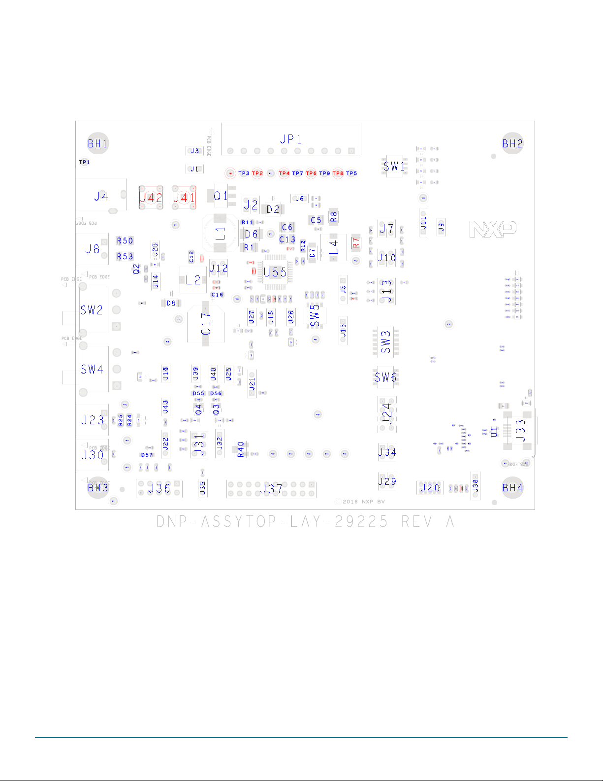
7 Board layout
7.1 Assembly layer top
Figure 25. Assembly layer top
Rev. 2
30 NXP Semiconductors
Page 31

7.2 Assembly layer bottom
Board layout
Figure 26. Assembly layer bottom
Rev. 2
NXP Semiconductors 31
Page 32

Board bill of materials
8 Board bill of materials
The schematic, board layout, and bill of materials for the evaluation boards are available at:
• www.nxp.com/KITFS4503CAEEVM
• www.nxp.com/KITFS4508CAEEVM
• www.nxp.com/KITFS6507LAEEVM
• www.nxp.com/KITFS6522LAEEVM
• www.nxp.com/KITFS6523CAEEVM
9 Accessory item bill of materials
Table 25. Accessory Bill of Materials
Item Qty Part number Description
1 1 10U2-03103BK USB cable A plug to USB mini B
2 1 1803659 10 ways PCB screw connector
3 3 1803578 2 ways PCB screw connector
Notes
2. NXP does not assume liability, endorse, or warrant components from external manufacturers are referenced in circuit drawings or tables. While
NXP offers component recommendations in this configuration, it is the customer’s responsibility to validate their application.
(2)
Rev. 2
32 NXP Semiconductors
Page 33

10 References
Table 26. References
NXP.com Support Pages Description URL
FS6500-FS4500 Data sheet TBD
AN4661
AN4388 Quad Flat Package (QFP) http://www.nxp.com/files/AN4388.pdf
Power dissipation tool (Excel file)
VCORE compensation network simulation board (CNC) upon demand
Non ISO pulses report upon demand
FMEDA FS6500/FS4500 FMEDA upon demand
FS4500-FS6500SMUG
KITFS4503CAEEVM
KITFS4508CAEEVM
KITFS6507LAEEVM
KITFS6522LAEEVM
KITFS6523CAEEVM
FS6500 Product summary page http://www.nxp.com/FS6500
FS4500 Product summary page http://www.nxp.com/FS4500
Analog home page http://www.nxp.com/analog
Designing the VCORE Compensation
Network
FS4500-FS6500SMUG safety manual
– User Guide
Tool Summary Page
http://www.nxp.com/AN4661.pdf
https://www.nxp.com/downloads/en/calculators/FS6500-FS4500-power-dissipation-calculator.xlsx
Available at DocStore
www.nxp.com/KITFS4503CAEEVM
www.nxp.com/KITFS4508CAEEVM
www.nxp.com/KITFS6507LAEEVM
www.nxp.com/KITFS6522LAEEVM
www.nxp.com/KITFS6523CAEEVM
References
Rev. 2
NXP Semiconductors 33
Page 34

Revision history
11 Revision history
Revision Date Description of Changes
1.0 5/2016 • Initial release
2.0 3/2021 • Added description for KITFS6507LAEEVM and KITFS4508CAEEVM evaluation boards
Rev. 2
34 NXP Semiconductors
Page 35

How to Reach Us:
Home Page:
NXP.com
Web Support:
http://www.nxp.com/support
Information in this document is provided solely to enable system and software implementers to use NXP products. There
are no expressed or implied copyright licenses granted hereunder to design or fabricate any integrated circuits based on
the information in this document. NXP reserves the right to make changes without further notice to any products herein.
NXP makes no warranty, representation, or guarantee regarding the suitability of its products for any particular purpose,
nor does NXP assume any liability arising out of the application or use of any product or circuit, and specifically disclaims
any and all liability, including without limitation, consequential or incidental damages. "Typical" parameters that may be
provided in NXP data sheets and/or specifications can and do vary in different applications, and actual performance may
vary over time. All operating parameters, including "typicals," must be validated for each customer application by the
customer's technical experts. NXP does not convey any license under its patent rights nor the rights of others. NXP sells
products pursuant to standard terms and conditions of sale, which can be found at the following address:
http://www.nxp.com/terms-of-use.html.
NXP, the NXP logo, Freescale, the Freescale logo and SMARTMOS are trademarks of NXP B.V. All other product or
service names are the property of their respective owners. All rights reserved.
© 2021 NXP B.V.
Document Number: KTFS4500-FS6500UG
Rev. 2
3/2021
 Loading...