

IW416
Dual-band 1x1 Wi-Fi 4 and Bluetooth 5.1 Combo SoC
Rev. 3 — 12 March 2021 Preliminary data sheet
1 Product overview
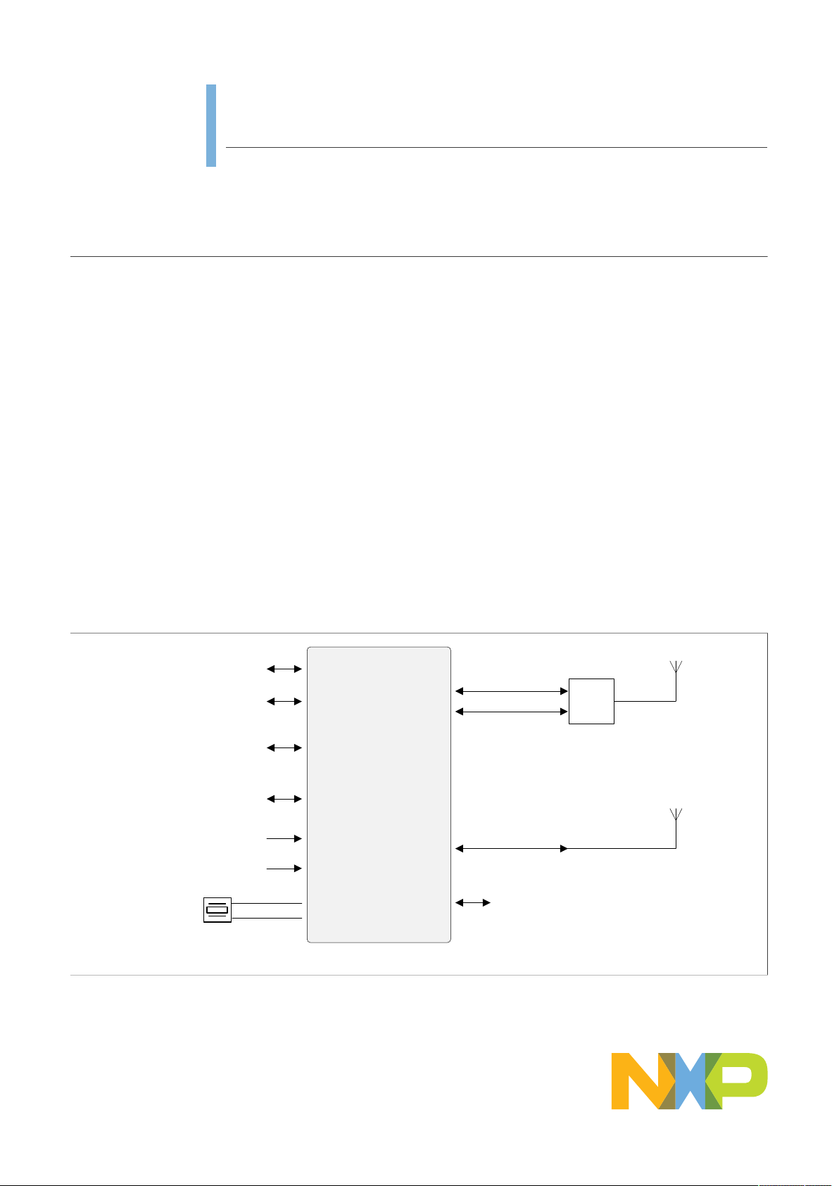
The IW416 is a highly integrated Wi-Fi 4 and Bluetooth 5.1 System-on-Chip (SoC)
enabling a low-cost connectivity solution. Supporting a 1x1 SISO Wi-Fi operation in the
2.4 GHz and the 5 GHz band, the SoC provides a full-feature Wi-Fi subsystem with a
peak PHY date rate of 150 Mbit/s. In addition to classic Bluetooth features, the IW416
enables Bluetooth 5.1 capabilities including Low Energy (LE), LE long range and LE data
up to 2 Mbit/s.
With integrated transmit (Tx) PAs, receive (Rx) LNAs and Tx/Rx switches for the Wi-Fi
and Bluetooth radios, the IW416 simplifies design allowing quick integration of either dual
or single-antenna operation. The dual-antenna configuration enables simultaneous Wi-Fi
and Bluetooth operation. With the single-antenna configuration, simultaneous 5 GHz WiFi and Bluetooth is supported and in the 2.4 GHz band, the single-antenna configuration
allows arbitrated transmit and receive operation of Wi-Fi and Bluetooth.
Promoting synergistic operation, the IW416 implements advanced Wi-Fi and Bluetooth
co-existence hardware in conjunction with algorithms to optimize collaborative
performance. In addition, support for external radio co-existence (e.g. cellular) is provided
through an external interface.
Available in both HVQFN and WLCSP packages with two operating temperature ranges
of 0 to 70°C and -40 to 85°C, the IW416 supports a SDIO host interface for the Wi-Fi
radio and a UART host interface for Bluetooth radio.
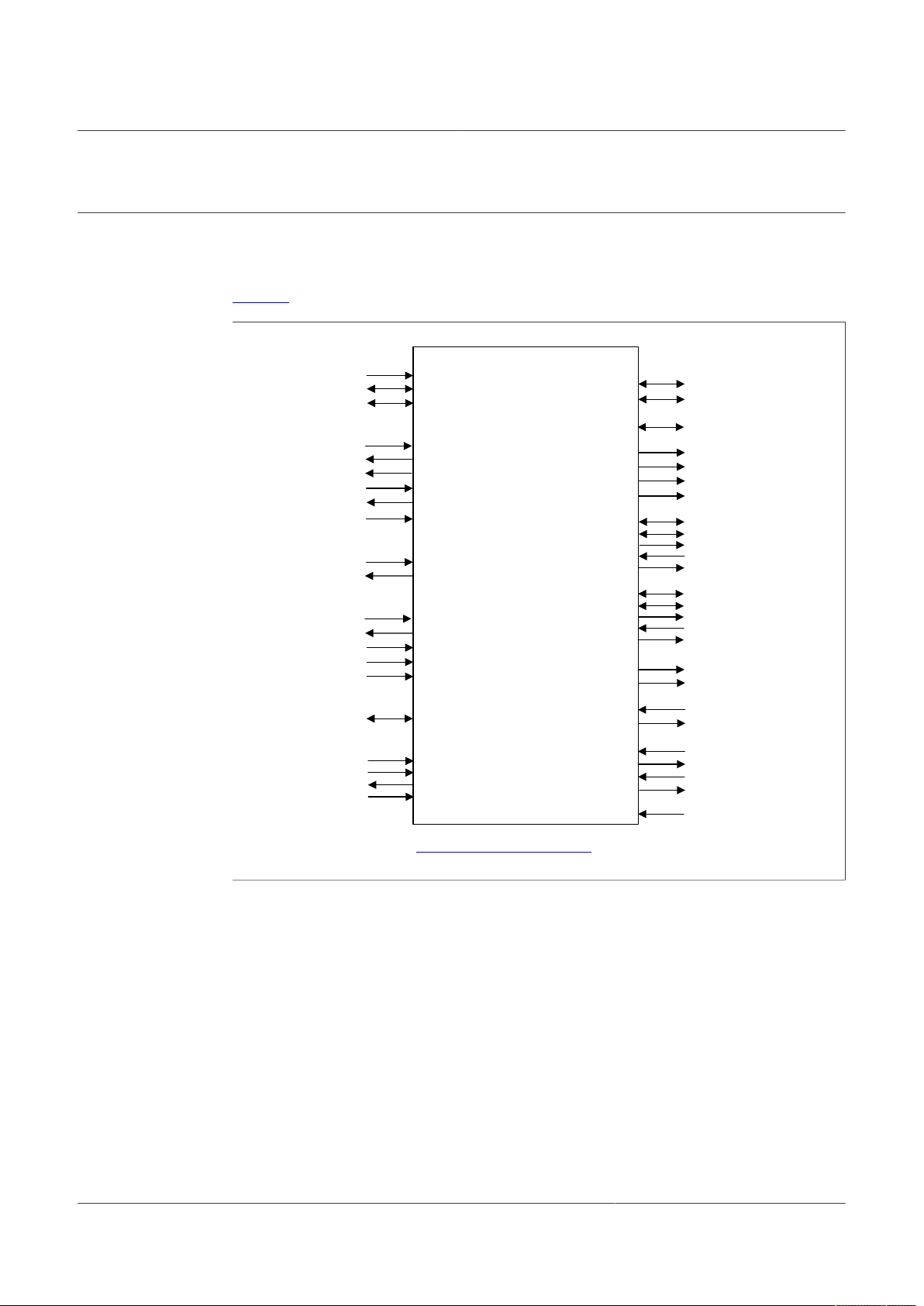
SDIO interface
UART interface
Audio interface
(I2S/PCM)
GPIO interface
Supply voltages
Power-down
XTAL_IN
XTAL_OUT
Figure 1. Application block diagram
IW416
Wi-Fi antenna
Wi-Fi 5 GHz Tx/Rx
Diplexer
Wi-Fi 2.4 GHz Tx/Rx
Bluetooth antenna
Bluetooth Tx/Rx
Coexistence

NXP Semiconductors
1.1 Applications
• Smart home: Voice assist device, smart printer, smart speaker, home automation
gateway, and IP camera
• Industrial and building automation
• Asset management
• Retail/POS
• Healthcare and medical devices
• Smart city
1.2 Wi-Fi key features
• Support 802.11 a/b/g/n
• Dual band: 2.4 GHz and 5 GHz
• Single stream 802.11n with 20 MHz and 40 MHz channels
• Up to MCS7 data rates (150 Mbit/s)
• Dynamic Rapid Channel Switching (DRCS) for simultaneous operation in 2.4 GHz and
5 GHz bands
• Interface to coexist with 802.15.4, LTE, or other radios
• Security: WPA3, WPA2, WPA2 and WPA mixed mode, WEP
IW416
Dual-band 1x1 Wi-Fi 4 and Bluetooth 5.1 Combo SoC
1.3 Bluetooth key features
• Full Bluetooth 5.1 features
• Long range - 4x coverage
• 2 Mbit/s data rate - 2x faster
• Improved advertisement capability - enables more IoT services
• I2S and PCM audio interfaces
• AES security
1.4 Host interfaces
Wi-Fi and Bluetooth host interface options
Wi-Fi Bluetooth
SDIO 3.0 UART
IW416 All information provided in this document is subject to legal disclaimers. © NXP B.V. 2021. All rights reserved.
Preliminary data sheet Rev. 3 — 12 March 2021
2 / 97

NXP Semiconductors
1.5 Operating characteristics
• Supply voltage: 1.05V, 1.8V, 2.2V and 3.3V (optional)
• Operating temperature:
– Commercial: 0 to 70°C
– Industrial: -40 to 85°C
1.6 General features
• Package options
– 68-pin HVQFN (8 mm x 8 mm)
– 76-bump WLCSP (3.95 mm x 3.565 mm)
• Simultaneous Wi-Fi and Bluetooth operation supported with dual antenna configuration
– Shared Wi-Fi and Bluetooth operation with single antenna is possible
• Power saving features
– Efficient power management system
– Sleep and standby modes
– Deep-sleep mode
• Independent ARM-based Wi-Fi and Bluetooth CPUs
– Wi-Fi CPU: 160 MHz clock speed
– Bluetooth CPU: 128 MHz clock speed
• Memory:
– Internal SRAM
– Boot ROM
– OTP memory to store the MAC address and calibration data
• Peripheral Interface
– General-Purpose I/O (GPIO) interface
IW416
Dual-band 1x1 Wi-Fi 4 and Bluetooth 5.1 Combo SoC
IW416 All information provided in this document is subject to legal disclaimers. © NXP B.V. 2021. All rights reserved.
Preliminary data sheet Rev. 3 — 12 March 2021
3 / 97
NXP Semiconductors
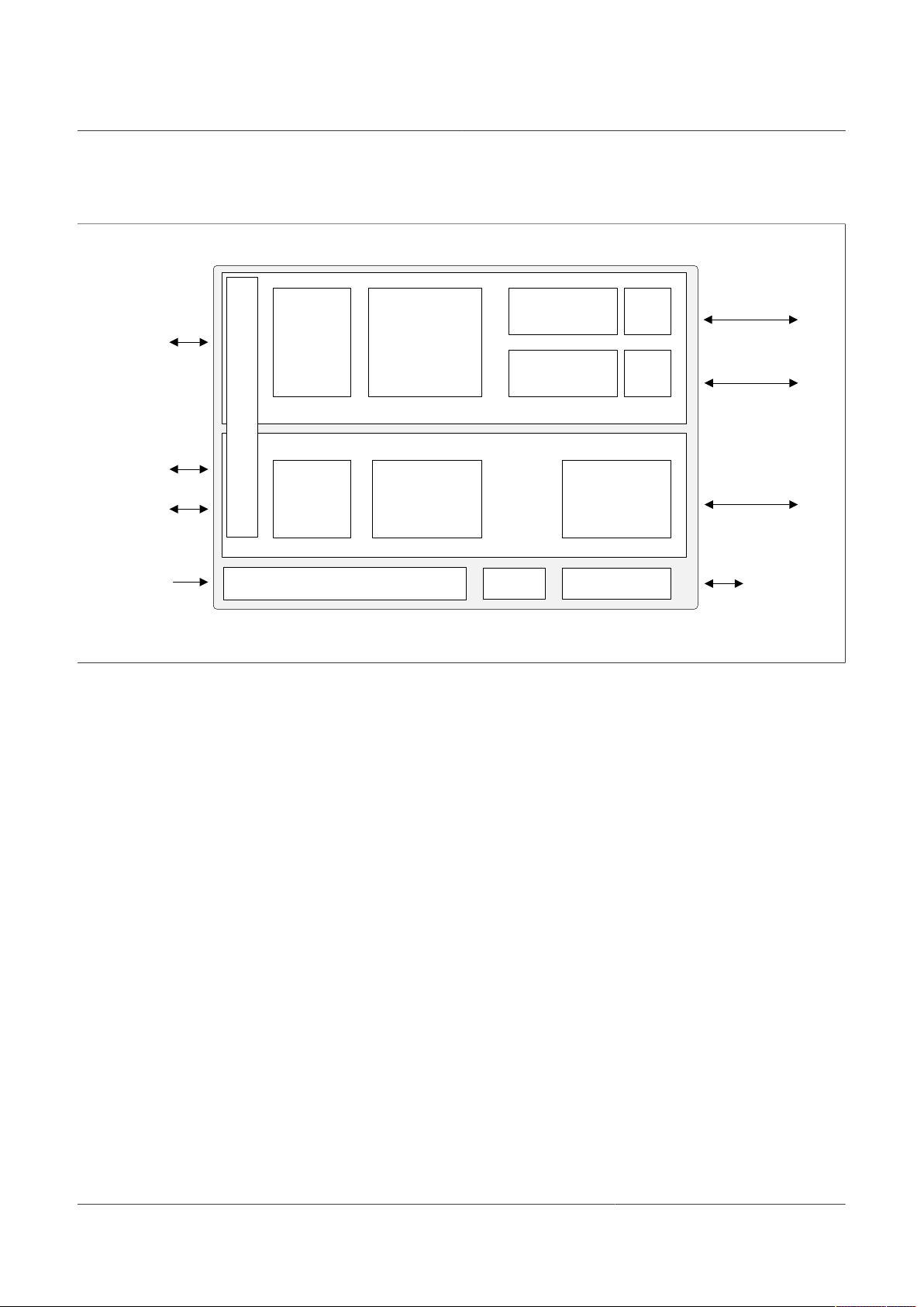
1.7 Internal block diagram
IW416
Dual-band 1x1 Wi-Fi 4 and Bluetooth 5.1 Combo SoC
SDIO 3.0
Host interface
UART
I2S/PCM
Supply voltages
Figure 2. Internal block diagram
Wi-Fi CPU
Bluetooth
CPU
Power regulator
Wi-Fi 4
MAC/Baseband
Bluetooth/
Bluetooth LE
Baseband
SPDT5 GHz PA/LNA
2.4 GHz PA/LNA SPDT
Bluetooth RF
CoexistenceOTP
Wi-Fi 5G Tx/Rx
Wi-Fi 2.4G Tx/Rx
Bluetooth Tx/Rx
Coexistence
IW416 All information provided in this document is subject to legal disclaimers. © NXP B.V. 2021. All rights reserved.
Preliminary data sheet Rev. 3 — 12 March 2021
4 / 97
NXP Semiconductors
2 Ordering information
IW416xx/xxxxx
IW416
Dual-band 1x1 Wi-Fi 4 and Bluetooth 5.1 Combo SoC
Packing code
Part number
Package code
Figure 3. Part numbering scheme
Table 1. Part order codes
Part order code Package type Operating
IW416HN/A1CK 68-pin HVQFN - 8 x 8 x 0.85 mm, with 0.4 mm pitch Commercial Tray
IW416HN/A1CMP 68-pin HVQFN - 8 x 8 x 0.85 mm, with 0.4 mm pitch Commercial Tape and Reel
IW416HN/A1IK 68-pin HVQFN - 8 x 8 x 0.85 mm, with 0.4 mm pitch Industrial Tray
IW416HN/A1IMP 68-pin HVQFN - 8 x 8 x 0.85 mm, with 0.4 mm pitch Industrial Tape and Reel
IW416UK/A1CZ 76-bump WLCSP - 3.95 x 3.565 x 0.495 mm Commercial Tape and Reel
IW416UK/A1IZ 76-bump WLCSP - 3.95 x 3.565 x 0.495 mm Industrial Tape and Reel
Temperature code
C = Commercial
I = Industrial
Die version
Packing
temperature range
IW416 All information provided in this document is subject to legal disclaimers. © NXP B.V. 2021. All rights reserved.
Preliminary data sheet Rev. 3 — 12 March 2021
5 / 97

NXP Semiconductors
3 Wi-Fi subsystem
3.1 IEEE 802.11 standards
• 802.11n maximum data rates up to 72 Mbit/s (20 MHz channel bandwidth), 150 Mbit/s
(40 MHz channel bandwidth)
• 802.11a/g/b backward compatibility
• 802.11d international roaming
• 802.11e quality of service
• 802.11h transmit power control
• 802.11h DFS radar pulse detection
• 802.11i enhanced security
• 802.11k radio resource measurement
• 802.11n block acknowledgment extension
• 802.11r fast hand-off for AP roaming
• 802.11u Hotspot 2.0 (STA mode only)
• 802.11v TIM frame transmission/reception
• 802.11w protected management frames
• Fully supports clients (stations) implementing IEEE Power Save mode
IW416
Dual-band 1x1 Wi-Fi 4 and Bluetooth 5.1 Combo SoC
3.2 Wi-Fi MAC
The Wi-Fi MAC has the following features:
• Simultaneous peer-to-peer and infrastructure modes
• RTS/CTS for operation under DCF
• Hardware filtering of 32 multicast addresses and duplicate frame detection for up to 32
unicast addresses
• On-chip Tx and Rx FIFO for maximum throughput
• Open System and Shared Key Authentication services
• A-MPDU Rx (de-aggregation) and Tx (aggregation)
• 20/40 MHz coexistence
• Reduced Inter-Frame Spacing (RIFS) receive
• Packet drop scheme
• Management information base counters
• Radio resource measurement counters
• Quality of service queues
• Block acknowledgment extension
• Dynamic frequency selection
• TIM frame transmission/reception
• Multiple BSS/Station
• Transmit rate adaptation
• Transmit power control
• Long and short preamble generation on a frame-by-frame basis for 802.11b frames
• NXP mobile hotspot
IW416 All information provided in this document is subject to legal disclaimers. © NXP B.V. 2021. All rights reserved.
Preliminary data sheet Rev. 3 — 12 March 2021
6 / 97

NXP Semiconductors
3.3 Wi-Fi baseband
The Wi-Fi baseband has the following features:
• 802.11n 1x1 SISO
• Bandwidth supported:
– 20 MHz
– 20 in 40 MHz (upper and lower)
– 40 MHz
– 20 MHz duplicate
• 802.11n modulation coding scheme (MCS) 0-7 and MCS 32 (HT duplicate mode)
• 802.11n 400 ns and 800 ns guard interval
• Dynamic frequency selection (radar detection)
– Enhanced radar detection for long and short pulse radar
– Enhanced AGC scheme for DFS channel
• Radio resource measurement
• Optional 802.11n SISO features:
– 20/40 MHz coexistence
– 1 spatial stream STBC reception
– Short guard interval
– RIFS on receive path for 802.11n packets
– 802.11n greenfield Tx/Rx
• Power save features
IW416
Dual-band 1x1 Wi-Fi 4 and Bluetooth 5.1 Combo SoC
3.4 Wi-Fi radio
The Wi-Fi radio has the following features:
• Integrated direct-conversion radio
• 20 MHz and 40 MHz channel bandwidths
Wi-Fi Rx path
• Direct conversion architecture: no need for an external SAW filter
• On-chip gain selectable LNA with optimized noise figure and power consumption
• High dynamic range AGC function in receive mode
Wi-Fi Tx path
• Internal PA with power control
• Optimized Tx gain distribution for linearity and noise performance
IW416 All information provided in this document is subject to legal disclaimers. © NXP B.V. 2021. All rights reserved.
Preliminary data sheet Rev. 3 — 12 March 2021
7 / 97
NXP Semiconductors
Radio channel frequencies
The Wi-Fi RF radio integrates all the necessary functions for transmit and receive
operation.
The channel frequencies are controlled through an internal bus and software
programmable.
Table 2 shows the frequencies supported by the 20 MHz channels.
Table 2. Frequencies supported by 20 MHz channels
Channel Frequency (GHz)
1 2.412
2 2.417
3 2.422
4 2.427
5 2.432
6 2.437
7 2.442
8 2.447
9 2.452
10 2.457
11 2.462
12 2.467
13 2.472
-- --
36 5.180
40 5.200
44 5.220
48 5.240
52 5.260
56 5.280
60 5.300
64 5.320
100 5.500
104 5.520
108 5.540
112 5.560
116 5.580
120 5.600
124 5.620
128 5.640
IW416
Dual-band 1x1 Wi-Fi 4 and Bluetooth 5.1 Combo SoC
IW416 All information provided in this document is subject to legal disclaimers. © NXP B.V. 2021. All rights reserved.
Preliminary data sheet Rev. 3 — 12 March 2021
8 / 97

NXP Semiconductors
Table 2. Frequencies supported by 20 MHz channels...continued
Channel Frequency (GHz)
132 5.660
136 5.680
140 5.700
149 5.745
153 5.765
157 5.785
161 5.805
165 5.825
128 5.640
132 5.660
136 5.680
140 5.700
149 5.745
153 5.765
157 5.785
161 5.805
165 5.825
IW416
Dual-band 1x1 Wi-Fi 4 and Bluetooth 5.1 Combo SoC
Table 3 shows the frequencies supported by the 40 MHz channels.
Table 3. Frequencies Supported by the 40 MHz channels
Channel Frequency (GHz)
1–5 2.422
2–6 2.427
3–7 2.432
4–8 2.437
5–9 2.442
6–10 2.447
7–11 2.452
-- --
36–40 5.190
44–48 5.230
52–56 5.270
60–64 5.310
100–104 5.510
108–112 5.550
116–120 5.590
124–128 5.630
IW416 All information provided in this document is subject to legal disclaimers. © NXP B.V. 2021. All rights reserved.
Preliminary data sheet Rev. 3 — 12 March 2021
9 / 97

NXP Semiconductors
Table 3. Frequencies Supported by the 40 MHz channels...continued
Channel Frequency (GHz)
132–136 5.670
149–153 5.755
157–161 5.795
3.5 Wi-Fi encryption
• WEP 64 bit and 128 bit encryption with hardware TKIP processing (WPA)
• AES/CCMP as part of the 802.11i security standard (WPA2 and WPA mixed mode)
• AES/CMAC as part of the 802.11w security standard
3.6 Wi-Fi host interfaces
• SDIO 3.0 device interface
IW416
Dual-band 1x1 Wi-Fi 4 and Bluetooth 5.1 Combo SoC
IW416 All information provided in this document is subject to legal disclaimers. © NXP B.V. 2021. All rights reserved.
Preliminary data sheet Rev. 3 — 12 March 2021
10 / 97

NXP Semiconductors
4 Bluetooth subsystem
4.1 Bluetooth 2.4 GHz Tx/Rx
• Bluetooth 5.1
• Bluetooth Class 2 and Bluetooth Class 1
• Single-ended, shared Tx/Rx path for Bluetooth
• PCM interface for voice applications
• Baseband and radio Basic Data Rate (BDR)/Enhanced Data Rate (EDR) packet types
—1 Mbit/s (GFSK), 2 Mbit/s (π/4-DQPSK), and 3 Mbit/s (8DPSK)
• Fully functional Bluetooth baseband—Adaptive Frequency Hopping (AFH), forward
error correction, header error control, access code correlation, Cyclic Redundancy
Check (CRC), encryption bit stream generation, and whitening
• Adaptive Frequency Hopping (AFH) using Packet Error Rate (PER)
• Interlaced scan for faster connection setup
• Simultaneous active Asynchronous Connection-Less (ACL) connection support
• Automatic ACL packet type selection
• Full master and slave piconet support
• Scatternet support
• Bluetooth-based indoor location with up to 16 antenna support
• Standard UART HCI transport layer
• HCI layer to integrate with profile stack
• SCO/eSCO links with hardware accelerated audio signal processing and hardware
supported PPEC algorithm for speech quality improvement
• All standard SCO/eSCO voice coding
• All standard pairing, authentication, link key, and encryption operations
• Standard Bluetooth power saving mechanisms (hold, sniff modes, and sniff sub-rating)
• Enhanced Power Control (EPC)
• Channel Quality Driven Data Rate (CQDDR)
• Wide Band Speech (WBS) support (2 WBS link)
• Encryption (AES) support
• Low Latency Reconnection (LLR) (future BT standard)
IW416
Dual-band 1x1 Wi-Fi 4 and Bluetooth 5.1 Combo SoC
IW416 All information provided in this document is subject to legal disclaimers. © NXP B.V. 2021. All rights reserved.
Preliminary data sheet Rev. 3 — 12 March 2021
11 / 97

NXP Semiconductors
4.2 Bluetooth Low Energy (LE)
• Broadcaster, Observer, Central, and Peripheral roles
• Supports link layer topology to be master and slave (connects up to 16 links)
• Wi-Fi/Bluetooth Coexistence protocol support
• Shared RF with BDR/EDR
• Encryption (AES) support
• Intelligent Adaptive Frequency Hopping (AFH)
• LE Privacy 1.2
• LE Secure Connection
• LE Data Length Extension
• LE Advertising Extension
• 2 Mbit/s LE
4.3 Bluetooth host interfaces
• High-Speed UART interface up to 4 Mbit/s
IW416
Dual-band 1x1 Wi-Fi 4 and Bluetooth 5.1 Combo SoC
4.4 Audio interfaces
4.4.1 I2S interface
• I2S (Inter-IC Sound) interface for audio data connection to Analog-to-Digital Converter
(ADC)
• Master and slave modes for I2S, MSB, and LSB audio interfaces
• Tri-state I2S interface compatibility
• I2S pins shared with PCM pins
4.4.2 PCM interface
The PCM interface is used to exchange audio data between the host and the Bluetooth/
LE functional block.
• Master or slave mode
• PCM bit width size of 8 bits or 16 bits
• Up to 4 slots with configurable bit width and start positions
• PCM short frame and long frame 1 synchronization
• Tri-state PCM interface capability
• PCM pins shared with I2S pins
1 In PCM Master mode, PCM long frame synchronization is 1 clock wide. In PCM Slave mode, PCM
Master’s long frame synchronization pattern is supported.
IW416 All information provided in this document is subject to legal disclaimers. © NXP B.V. 2021. All rights reserved.
Preliminary data sheet Rev. 3 — 12 March 2021
12 / 97

NXP Semiconductors
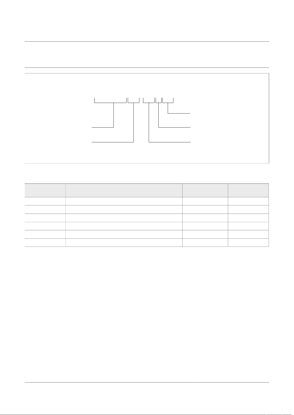
aaa- 036047
CLK
DOUT
SYNC
DIN
MSb MSb-1 MSb-2 MSb-3 d1
d1 d0
d0
MSbDon't Care Don't CareMSb-1 MSb-2 MSb-3
4.4.2.1 Protocol description
The PCM interface supports short frame sync. Figure 4 shows an example of a PCM
interface with 4 signals.
Figure 4. PCM Short Frame Sync
4.5 Coexistence
The advanced coexistence framework provides packet traffic arbitration (PTA) for the
following use cases:
IW416
Dual-band 1x1 Wi-Fi 4 and Bluetooth 5.1 Combo SoC
• Coexistence between internal Wi-Fi and internal Bluetooth radios
• Coexistence between internal Wi-Fi and Bluetooth radios and an external radio such
as 802.15.4, LTE or 5G. The external radio can be connected to the PTA interface or
WCI-2 interface. WCI-2 message format and message type comply with Bluetooth
special interest group (SIG) core specification volume 7 part C.
IW416 All information provided in this document is subject to legal disclaimers. © NXP B.V. 2021. All rights reserved.
Preliminary data sheet Rev. 3 — 12 March 2021
13 / 97
NXP Semiconductors
5 Pin information
5.1 Signal diagram
Figure 5 shows the signals for the device. Some signals are muxed through GPIO.
IW416
Dual-band 1x1 Wi-Fi 4 and Bluetooth 5.1 Combo SoC
SD_CLK
SD_CMD
SD_DAT[3:0]
UART_SIN
UART_SOUT
UART_RTSn
UART_CTSn
UART_DTRn
UART_DSRn
WCI-2_SIN
WCI-2_SOUT
EXT_STATE
EXT_GNT
EXT_FREQ
EXT_PRI
EXT_REQ
GPIO[15:0]
JTAG_TCK
JTAG_TDI
JTAG_TDO
JTAG_TMS
SDIO Interface
UART Interface
(through GPIO)
WCI-2 interface
PTA interface
GPIO Interface
JTAG Interface
(through GPIO)
IW416
Wi-Fi Radio Interface
Bluetooth Radio Interface
RF Front End
Control Interface
I2S Interface
(through GPIO)
PCM Interface
(through GPIO)
Power Management
Interface
(through GPIO)
LDO Interface
Clock Interface
RF_TR_2
RF_TR_5
BRF_ANT
RF_CNTL0_N
RF_CNTL1_P
RF_CNTL2_N
RF_CNTL3_P
I2S_LRCLK
I2S_BCLK
I2S_DOUT
I2S_DIN
I2S_CCLK
PCM_SYNC
PCM_CLK
PCM_MCLK
PCM_DIN
PCM_DOUT
DVSC[0]
DVSC[1]
LDO_VIN
LDO_VOUT
XTAL_IN
XTAL_OUT
SLP_CLK_IN
XOSC_EN
PDnPower-down
Signals may be muxed. See Section 5.5 "Pin description".
Figure 5. Signal diagram
IW416 All information provided in this document is subject to legal disclaimers. © NXP B.V. 2021. All rights reserved.
Preliminary data sheet Rev. 3 — 12 March 2021
14 / 97
NXP Semiconductors
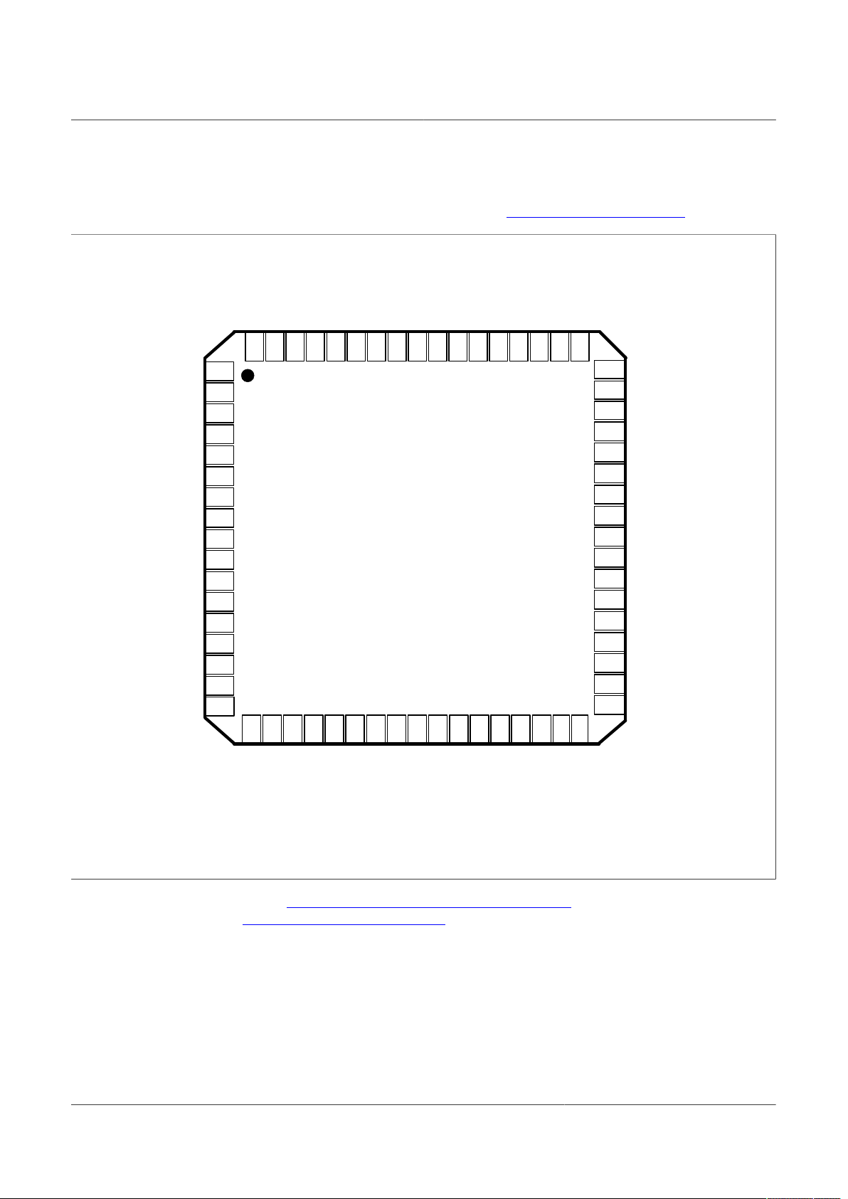
5.2 Pin assignment - 68-pin HVQFN package
Note that some pins have muxed signals. See Section 5.5 "Pin description".
IW416
Dual-band 1x1 Wi-Fi 4 and Bluetooth 5.1 Combo SoC
AVDD33
AVDD18
DNC
DNC
GPIO[9]
GPIO[10]
VIO
GPIO[11]
GPIO[12]
GPIO[13]
GPIO[0]
VCORE
VIO_RF
RF_CNTL1_P
RF_CNTL0_N
RF_CNTL3_P
RF_CNTL2_N
SD_CMD
62
24
LDO_VOUT
LDO_VIN
60
61
IW416
26
25
VCORE
PDn
AVDD18
GPIO[6]
GPIO[2]
GPIO[4]
GPIO[3]
55
56
57
58
59
31
30
29
28
27
GPIO[1]
52
53
54
51
VIO
50
GPIO[7]
49
GPIO[5]
48
GPIO[14]
GPIO[15]
47
GPIO[8]
46
45
WCI-2_SOUT
44
WCI-2_SIN
43
DNC
42
SLP_CLK_IN
41
AVDD18
XTAL_OUT
40
39
XTAL_IN
38
AVDD18
37
AVDD18
36
AVDD18
35
AVSS
34
32
33
SD_DAT[3]
68
66
67
1
2
3
4
5
6
7
8
9
10
11
12
13
14
15
16
17
20
19
18
SD_CLK
63
64
65
23
22
21
VIO_SD
SD_DAT[0]
SD_DAT[1]
SD_DAT[2]
NC
NC
AVDD18
AVDD18
AVDD18
VCORE
BRF_ANT
RF_TR_2
NC
VPA
VPA
AVDD18
AVDD18
RF_TR_5
NC
NC
NC
Figure 6. Pin assignment (package top view)
Note: See Section 9.10 "Reference clock specifications" for electrical specifications.
See Section 10.3 "Package marking" for more information on package marking and pin 1
location.
IW416 All information provided in this document is subject to legal disclaimers. © NXP B.V. 2021. All rights reserved.
Preliminary data sheet Rev. 3 — 12 March 2021
15 / 97

NXP Semiconductors
5.2.1 Pin list by number
The following table shows the pin list sorted by pin number.
Table 4. Pin list by number
Pin number Pin name Power Type
1 AVDD33 -- Power
2 AVDD18 -- Power
3 DNC — DNC
4 DNC — DNC
5 GPIO[9] VIO I/O
5 DNC — Do not connect
6 GPIO[10] VIO I/O
7 VIO -- Power
8 GPIO[11] VIO I/O
9 GPIO[12] VIO I/O
10 GPIO[13] VIO I/O
11 GPIO[0] VIO I/O
12 VCORE -- Power
13 VIO_RF -- Power
14 RF_CNTL1_P VIO_RF O
15 RF_CNTL0_N VIO_RF O
16 RF_CNTL3_P VIO_RF O
17 RF_CNTL2_N VIO_RF O
18 AVDD18 -- Power
19 AVDD18 -- Power
20 AVDD18 -- Power
21 BRF_ANT AVDD18 A, I/O
22 NC -- NC
23 VCORE -- Power
24 NC -- NC
25 RF_TR_2 AVDD18 A, I/O
26 AVDD18 -- Power
27 NC -- NC
28 VPA -- Power
29 VPA -- Power
30 RF_TR_5 AVDD18 A, I/O
31 AVDD18 -- Power
32 NC -- NC
33 NC -- NC
IW416
Dual-band 1x1 Wi-Fi 4 and Bluetooth 5.1 Combo SoC
IW416 All information provided in this document is subject to legal disclaimers. © NXP B.V. 2021. All rights reserved.
Preliminary data sheet Rev. 3 — 12 March 2021
16 / 97

NXP Semiconductors
Table 4. Pin list by number...continued
Pin number Pin name Power Type
34 NC -- NC
35 AVSS -- Ground
36 AVDD18 -- Power
37 AVDD18 -- Power
38 AVDD18 -- Power
39 XTAL_IN AVDD18 A, I/O
40 XTAL_OUT AVDD18 A, I/O
41 AVDD18 -- Power
42 SLP_CLK_IN AVDD18 I
43 DNC -- DNC
44 WCI-2_SIN AVDD18 I
45 WCI-2_SOUT AVDD18 O
46 GPIO[8] VIO I/O
47 GPIO[15] VIO I/O
48 GPIO[14] VIO I/O
49 GPIO[5] VIO I/O
50 GPIO[7] VIO I/O
51 VIO -- Power
52 GPIO[1] VIO I/O
53 GPIO[4] VIO I/O
54 GPIO[2] VIO I/O
55 GPIO[6] VIO I/O
56 GPIO[3] VIO I/O
57 AVDD18 -- Power
58 PDn AVDD18 I
59 VCORE -- Power
60 LDO_VOUT -- Power
61 LDO_VIN -- Power
62 SD_CMD VIO_SD I/O
63 SD_CLK VIO_SD I
64 VIO_SD -- Power
65 SD_DAT[0] VIO_SD I/O
66 SD_DAT[1] VIO_SD I/O
67 SD_DAT[2] VIO_SD I/O
68 SD_DAT[3] VIO_SD I/O
IW416
Dual-band 1x1 Wi-Fi 4 and Bluetooth 5.1 Combo SoC
IW416 All information provided in this document is subject to legal disclaimers. © NXP B.V. 2021. All rights reserved.
Preliminary data sheet Rev. 3 — 12 March 2021
17 / 97

NXP Semiconductors
5.2.2 Pin list by name
The following table shows the pin list sorted by pin name.
Table 5. Pin by name
Pin name Pin number Power Type
AVDD18 2 -- Power
AVDD18 18 -- Power
AVDD18 19 -- Power
AVDD18 20 -- Power
AVDD18 26 -- Power
AVDD18 31 -- Power
AVDD18 36 -- Power
AVDD18 37 -- Power
AVDD18 38 -- Power
AVDD18 41 -- Power
AVDD18 57 -- Power
AVDD33 1 -- Power
AVSS 35 -- Ground
BRF_ANT 21 AVDD18 A, I/O
DNC 43 -- DNC
GPIO[0] 11 VIO I/O
GPIO[1] 52 VIO I/O
GPIO[10] 6 VIO I/O
GPIO[11] 8 VIO I/O
GPIO[12] 9 VIO I/O
GPIO[13] 10 VIO I/O
GPIO[14] 48 VIO I/O
GPIO[15] 47 VIO I/O
GPIO[2] 54 VIO I/O
GPIO[3] 56 VIO I/O
GPIO[4] 53 VIO I/O
GPIO[5] 49 VIO I/O
GPIO[6] 55 VIO I/O
GPIO[7] 50 VIO I/O
GPIO[8] 46 VIO I/O
GPIO[9] 5 VIO I/O
LDO_VIN 61 -- Power
LDO_VOUT 60 -- Power
NC 22 -- NC
IW416
Dual-band 1x1 Wi-Fi 4 and Bluetooth 5.1 Combo SoC
IW416 All information provided in this document is subject to legal disclaimers. © NXP B.V. 2021. All rights reserved.
Preliminary data sheet Rev. 3 — 12 March 2021
18 / 97

NXP Semiconductors
Table 5. Pin by name...continued
Pin name Pin number Power Type
NC 24 -- NC
NC 27 -- NC
NC 32 -- NC
NC 33 -- NC
NC 34 -- NC
PDn 58 AVDD18 I
RF_CNTL0_N 15 VIO_RF O
RF_CNTL1_P 14 VIO_RF O
RF_CNTL2_N 17 VIO_RF O
RF_CNTL3_P 16 VIO_RF O
RF_TR_2 25 AVDD18 A, I/O
RF_TR_5 30 AVDD18 A, I/O
SD_CLK 63 VIO_SD I
SD_CMD 62 VIO_SD I/O
SD_DAT[0] 65 VIO_SD I/O
SD_DAT[1] 66 VIO_SD I/O
SD_DAT[2] 67 VIO_SD I/O
SD_DAT[3] 68 VIO_SD I/O
SLP_CLK_IN 42 AVDD18 I
DNC 4 — DNC
DNC 3 — DNC
VCORE 12 -- Power
VCORE 23 -- Power
VCORE 59 -- Power
VIO 7 -- Power
VIO 51 -- Power
VIO_RF 13 -- Power
VIO_SD 64 -- Power
VPA 28 -- Power
VPA 29 -- Power
WCI-2_SIN 44 AVDD18 I
WCI-2_SOUT 45 AVDD18 O
XTAL_IN 39 AVDD18 A, I/O
XTAL_OUT 40 AVDD18 A, I/O
IW416
Dual-band 1x1 Wi-Fi 4 and Bluetooth 5.1 Combo SoC
IW416 All information provided in this document is subject to legal disclaimers. © NXP B.V. 2021. All rights reserved.
Preliminary data sheet Rev. 3 — 12 March 2021
19 / 97
NXP Semiconductors
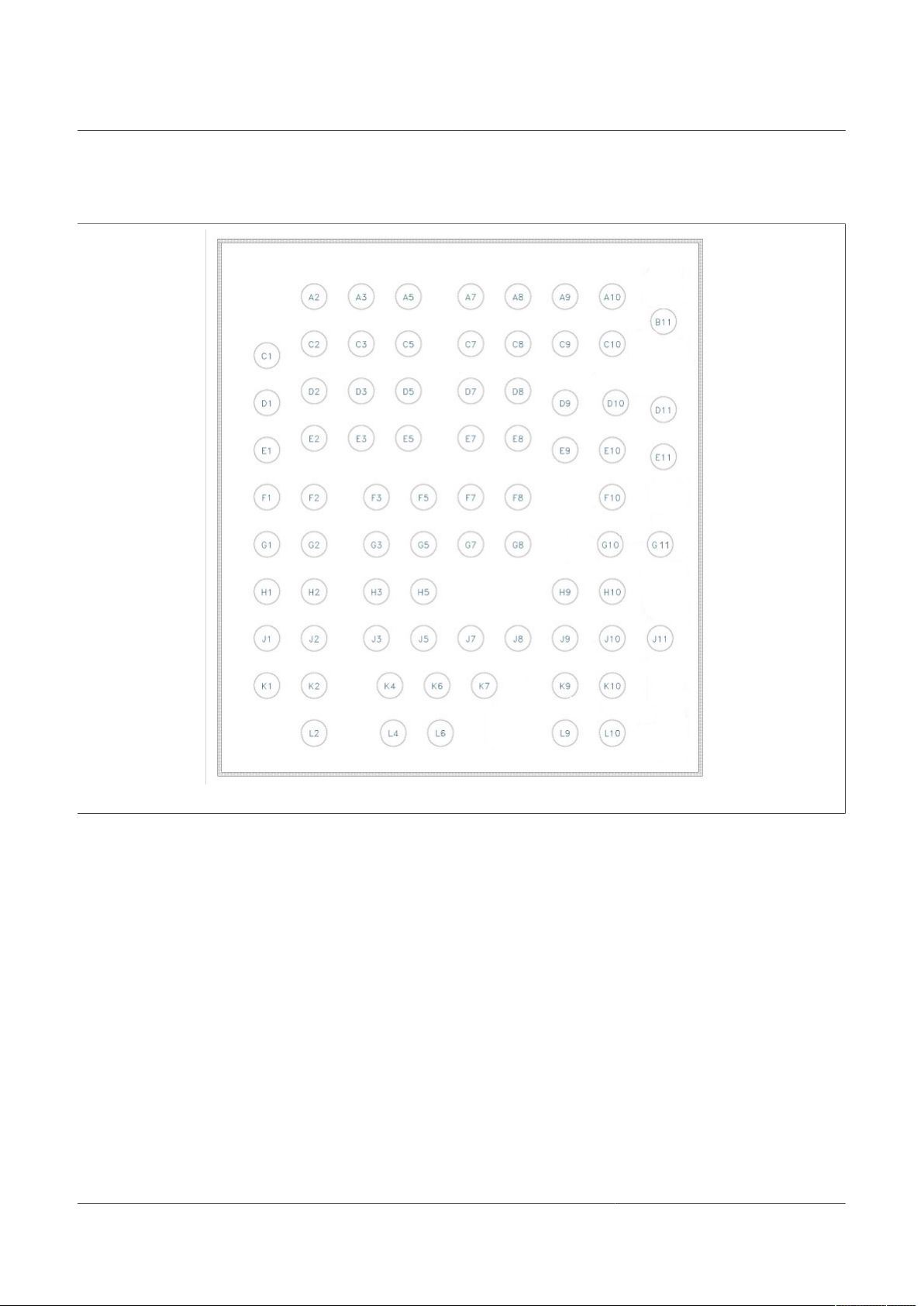
5.3 Bump locations - 76-bump WLCSP package
IW416
Dual-band 1x1 Wi-Fi 4 and Bluetooth 5.1 Combo SoC
Figure 7. Bump locations - 76-bump WLCSP (non-bump side view, bumps down)
IW416 All information provided in this document is subject to legal disclaimers. © NXP B.V. 2021. All rights reserved.
Preliminary data sheet Rev. 3 — 12 March 2021
20 / 97

NXP Semiconductors
IW416
Dual-band 1x1 Wi-Fi 4 and Bluetooth 5.1 Combo SoC
5.3.1 Bump positions relative to die center
Table 6. Bump names and locations on 76-bump WLCSP top view
Alpha-numeric
designation
A2 SD_DAT[1] -1080.696 1562.352
A3 SD_DAT[3] -730.696 1562.352
A5 VIO -380.696 1562.352
A7 VIO_RF 81.805 1562.352
A8 RF_CNTL1_P 431.805 1562.352
A9 AVDD18 781.805 1562.352
A10 AVDD18 1131.805 1562.352
B11 VSS 1506.805 1377.352
C1 LDO_VIN -1430.696 1124.852
C2 VIO_SD -1080.696 1212.352
C3 SD_DAT[2] -730.696 1212.352
C5 VCORE -380.696 1212.352
C7 GPIO[0] 81.805 1212.352
C8 VSS 431.805 1212.352
C9 VSS 781.805 1212.352
C10 VSS 1131.805 1212.352
D1 LDO_VOUT -1430.696 774.852
D2 SD_CLK -1080.696 862.352
D3 SD_DAT[0] -730.696 862.352
D5 GPIO[10] -380.696 862.352
D7 GPIO[13] 81.805 862.352
D8 RF_CNTL0_N 431.805 862.352
D9 RF_CNTL3_P 781.805 774.852
D10 VSS 1156.805 774.852
D11 BRF_ANT 1506.805 724.852
E1 VCORE -1430.696 424.852
E2 SD_CMD -1080.696 512.352
E3 VSS -730.696 512.352
E5 GPIO[9] -380.696 512.352
E7 GPIO[11] 81.805 512.352
E8 GPIO[12] 431.805 512.352
E9 RF_CNTL2_N 781.805 424.852
E10 VSS 1131.805 424.852
Signal name
Bump location relative to die
center (non-bump side view)
X ( um ) Y ( um )
IW416 All information provided in this document is subject to legal disclaimers. © NXP B.V. 2021. All rights reserved.
Preliminary data sheet Rev. 3 — 12 March 2021
21 / 97
NXP Semiconductors
IW416
Dual-band 1x1 Wi-Fi 4 and Bluetooth 5.1 Combo SoC
Table 6. Bump names and locations on 76-bump WLCSP top view...continued
Alpha-numeric
designation
E11 AVDD18 1506.805 374.852
F1 VSS -1430.696 74.852
F2 GPIO[3] -1080.696 74.852
F3 GPIO[7] -618.196 74.852
F5 VSS -268.196 74.852
F7 WCI-2_SOUT 81.805 74.852
F8 WCI-2_SIN 431.805 74.852
F10 VSS 1131.805 74.852
G1 GPIO[6] -1430.696 -275.148
G2 GPIO[4] -1080.696 -275.148
G3 GPIO[5] -618.196 -275.148
G5 GPIO[14] -268.196 -275.148
G7 SLP_CLK_IN 81.805 -275.148
G8 DNC 431.805 -275.148
G10 AVDD18 1116.805 -275.148
G11 RF_TR_2 1481.805 -275.148
H1 PDn -1430.696 -625.148
H2 GPIO[1] -1080.696 -625.148
H3 GPIO[8] -618.196 -625.148
H5 VSS -268.196 -625.148
H9 VCORE 781.805 -625.148
H10 VSS 1131.805 -625.148
J1 AVDD18 -1430.696 -975.148
J2 VSS -1080.696 -975.148
J3 AVDD18 -618.196 -975.148
J5 VSS -268.196 -975.148
J7 VSS 81.805 -975.148
J8 VSS 431.805 -975.148
J9 VSS 781.805 -975.148
J10 VPA 1131.805 -975.148
J11 RF_TR_5 1481.805 -975.148
K1 GPIO[2] -1430.696 -1325.148
K2 VIO -1080.696 -1325.148
K4 XTAL_OUT -518.196 -1325.148
K6 VSS -168.196 -1325.148
IW416 All information provided in this document is subject to legal disclaimers. © NXP B.V. 2021. All rights reserved.
Preliminary data sheet Rev. 3 — 12 March 2021
Signal name
Bump location relative to die
center (non-bump side view)
X ( um ) Y ( um )
22 / 97
NXP Semiconductors
IW416
Dual-band 1x1 Wi-Fi 4 and Bluetooth 5.1 Combo SoC
Table 6. Bump names and locations on 76-bump WLCSP top view...continued
Alpha-numeric
designation
K7 AVDD18 181.805 -1325.148
K9 VSS 781.805 -1325.148
K10 VSS 1131.805 -1325.148
L2 GPIO[15] -1080.696 -1675.148
L4 XTAL_IN -493.196 -1675.148
L6 AVDD18 -143.195 -1675.148
L9 AVDD18 781.805 -1675.148
L10 VSS 1131.805 -1675.148
Signal name
Bump location relative to die
center (non-bump side view)
X ( um ) Y ( um )
IW416 All information provided in this document is subject to legal disclaimers. © NXP B.V. 2021. All rights reserved.
Preliminary data sheet Rev. 3 — 12 March 2021
23 / 97

NXP Semiconductors
5.4 Pin types
Table 7. Pin types
Pin type Description
I/O Digital input/output
I Digital input
O Digital output
A, I Analog input
A,O Analog output
A, I/O Analog input/output
NC No connect
DNC Do not connect
Power Power
Ground Ground
IW416
Dual-band 1x1 Wi-Fi 4 and Bluetooth 5.1 Combo SoC
5.5 Pin description
5.5.1 Pin states
The pin state information provided in the tables includes:
• No Pad Power State indicates the state when there is no power.
• PwrDwn State denotes the power-down state in default configuration. Many pads have
programmable power-down values, which can be set by firmware.
• Reset State is the state after the power-on-reset state and before the hardware state
(HW State).
• HW State (hardware state) is the state after boot code finishes and before firmware
download begins (firmware may change the pin state). HW State may differ based on
the pin muxing/strap setting. For example, for UART_RTSn and UART_SOUT, the boot
code will enable the UART interface when the device is in SDIO-UART mode, making
the HW states output high and output low, respectively.
• PwrDwn Prog indicates if the power-down state can be programmed.
• PU denotes whether the pull-up can be programmed or not.
• PD denotes whether the pull-down can be programmed or not.
• Pull-up and pull-down are only effective when the pad is in input mode.
• After firmware is downloaded, the pads (GPIO, RF control, and so on) are programmed
in functional mode per the functionality of the pins.
IW416 All information provided in this document is subject to legal disclaimers. © NXP B.V. 2021. All rights reserved.
Preliminary data sheet Rev. 3 — 12 March 2021
24 / 97

NXP Semiconductors
IW416
Dual-band 1x1 Wi-Fi 4 and Bluetooth 5.1 Combo SoC
5.5.2 General purpose I/O (GPIO) (MFP)
Table 8. GPIO
Pins may be Multi-Functional Pins (MFP).
Pin Name Supply No Pad
GPIO[15] VIO tristate input input drive high yes nominal PU yes yes
GPIO mode: GPIO[15] (input/output)
JTAG mode: JTAG_TMS - JTAG test mode select (input). See Section 5.5.13 "JTAG interface".
Reset recovery mode: Independent software reset for Bluetooth subsystem (input)
GPIO[14] VIO tristate input input tristate yes nominal PU yes yes
GPIO mode: GPIO[14] (input/output)
JTAG mode: JTAG_TCK - JTAG test clock (input). See Section 5.5.13 "JTAG interface".
Reset recovery mode: Independent software reset for Wi-Fi subsystem (input)
GPIO[13] VIO tristate input input drive high yes nominal PU yes yes
GPIO mode: GPIO[13] (input/output)
UART mode: UART_DTRn - UART data-terminal-ready (output). See Section 5.5.6 "UART host interface".
Out-of-band wake-up mode: Host to IW416 Wi-Fi wake-up (input)
GPIO[12] VIO tristate input input tristate yes nominal PU yes yes
GPIO mode: GPIO[12] (input/output)
UART mode: UART_DSRn - UART data-set-ready (input) (active low).See Section 5.5.6 "UART host interface".
Host wake-up mode: Host to IW416 Bluetooth wake-up (input)
GPIO[11] VIO tristate output input drive high yes weak PU yes yes
GPIO mode: GPIO[11] (input/output)
This pin is used as a configuration pin: CON[8] (input)
See Section 5.6 "Configuration pins".
UART mode: UART_RTSn - UART request-to-send (output) (active low). See Section 5.5.6 "UART host interface".
GPIO[10] VIO tristate input input tristate yes nominal PU yes yes
GPIO mode: GPIO[10] (input/output)
UART mode: UART_SOUT - UART serial (output). See Section 5.5.6 "UART host interface".
GPIO[9] VIO tristate output input tristate yes nominal PU yes yes
GPIO mode: GPIO[9] (input/output)
UART mode: UART_SIN - UART serial (input). See Section 5.5.6 "UART host interface".
GPIO[8] VIO tristate input input drive low yes weak PU yes yes
GPIO mode: GPIO[8] (input/output)
This pin is used as a configuration pin: CON7 (input)
See Section 5.6 "Configuration pins".
UART mode: UART_CTSn - UART clear-to-send input signal (input, active low). See Section 5.5.6 "UART host interface".
GPIO[7] VIO tristate input input tristate yes nominal PU yes yes
GPIO mode: GPIO[7] (input/output)
PCM mode: PCM_SYNC - PCM frame sync (input if slave, output if master). See Section 5.5.7 "Audio interface".
I2S mode: I2S_LRCLK - I2S left-right clock (input if slave, output if master). See Section 5.5.7 "Audio interface".
PTA mode: EXT_REQ - Request from the external radio (input). See Section 5.5.8 "PTA interface".
[1]
(MFP)
Power
State
Reset
State
HW State PwrDwn
State
PwrDwn
Prog
Internal PU/PDPU PD
IW416 All information provided in this document is subject to legal disclaimers. © NXP B.V. 2021. All rights reserved.
Preliminary data sheet Rev. 3 — 12 March 2021
25 / 97
NXP Semiconductors
IW416
Dual-band 1x1 Wi-Fi 4 and Bluetooth 5.1 Combo SoC
Table 8. GPIO
[1]
(MFP)...continued
Pins may be Multi-Functional Pins (MFP).
Pin Name Supply No Pad
Power
Reset
State
HW State PwrDwn
State
PwrDwn
Prog
Internal PU/PDPU PD
State
GPIO[6] VIO tristate input input tristate yes nominal PU yes yes
GPIO mode: GPIO[6] (input/output)
PCM mode: PCM_CLK - PCM data clock (input if slave, output if master). See Section 5.5.7 "Audio interface".
I2S mode: I2S_BCLK - I2S bit clock (input if slave, output if master). See Section 5.5.7 "Audio interface".
PTA mode: EXT_PRI - External radio priority signal (input). See Section 5.5.8 "PTA interface".
GPIO[5] VIO tristate input input tristate yes weak PU yes yes
GPIO mode: GPIO[5] (input/output)
PCM mode: PCM_DIN
[2]
- PCM receive signal (input). See Section 5.5.7 "Audio interface".
I2S mode: I2S_DOUT/I2S_DIN - I2S transmit/receive signal (output/input) (depending on the configuration). See
Section 5.5.7 "Audio interface".
PTA mode: EXT_GNT - External radio grant signal (output). See Section 5.5.8 "PTA interface".
GPIO[4] VIO tristate output input tristate yes nominal PU yes yes
GPIO mode: GPIO[4] (input/output)
PCM mode: PCM_DOUT
[3]
- PCM transmit signal (output). See Section 5.5.7 "Audio interface".
I2S mode: I2S_DOUT/I2S_DIN (depending on the configuration. If GPIO[5] is configured as I2S_DIN, then GPIO[4] is set
as I2S_DOUT, and vice-verse). See Section 5.5.7 "Audio interface".
PTA mode: EXT_FREQ - External radio frequency signal (input). See Section 5.5.8 "PTA interface".
Out-of-band wake-up mode: IW416 Bluetooth to host wake-up signal (output)
[4]
GPIO[3] VIO tristate input input tristate yes weak PU yes yes
GPIO mode: GPIO[3] (input/output)
Power management mode: DVSC[1], Digital voltage scaling control (output)
JTAG mode: JTAG_TDO, JTAG test data (output). See Section 5.5.13 "JTAG interface".
PCM mode: PCM_MCLK (output) - PCM clock signal (output, optional). See Section 5.5.7 "Audio interface".
I2S mode: I2S_CCLK - I2S clock (output, optional). See Section 5.5.7 "Audio interface".
GPIO[2] VIO tristate input input tristate yes weak PU yes yes
GPIO mode: GPIO[2] (input/output)
Power management mode: DVSC[0], Digital voltage scaling control (output)
JTAG mode: JTAG_TDI, JTAG test data (input). See Section 5.5.13 "JTAG interface".
GPIO[1] VIO tristate input input tristate yes weak PU yes yes
GPIO mode: GPIO[1] (input/output)
This pin is used as a configuration pin: CON[9] (input). See Section 5.6 "Configuration pins".
PTA mode: EXT_STATE - External radio state signal (input). See Section 5.5.8 "PTA interface".
Out-of-band wake-up mode: IW416 Wi-Fi to host wake-up signal (output)
GPIO[0] VIO tristate output output drive low yes nominal PU yes yes
GPIO mode: GPIO[0] (input/output)
Oscillator enable mode: XOSC_EN (output) (active high). See Section 5.5.10 "Clock interface".
[1] Not all GPIO pins can be used for Host-to-SoC wake-up signals.
[2] The function can be swapped with GPIO[4] using a software command without affecting the hardware connection.
[3] The function can be swapped with GPIO[5] using a software command without affecting the hardware connection.
[4] If PCM and UART interfaces are used in application, use GPIO[0] as alternative for this wake-up signal
IW416 All information provided in this document is subject to legal disclaimers. © NXP B.V. 2021. All rights reserved.
Preliminary data sheet Rev. 3 — 12 March 2021
26 / 97
NXP Semiconductors
IW416
Dual-band 1x1 Wi-Fi 4 and Bluetooth 5.1 Combo SoC
5.5.3 Wi-Fi/Bluetooth radio interface
Table 9. Wi-Fi/Bluetooth radio interface
Pin Name Type Supply Description
RF_TR_2 A, I/O AVDD18 Wi-Fi Transmit/Receive (2.4 GHz)
RF_TR_5 A, I/O AVDD18 Wi-Fi Transmit/Receive (5 GHz)
BRF_ANT A, I/O AVDD18 Bluetooth Transmit/Receive
5.5.4 Wi-Fi RF front-end control interface
Table 10. Wi-Fi RF front-end control interface
Pin Name Supply No Pad
Power
State
RF_CNTL0_N VIO_RF tristate input output drive low yes weak PU no no
RF Control 0—RF Control Output Low (output)
This pin is used as a configuration pin: CON[0] (input)
See Section 5.6 "Configuration pins".
RF_CNTL1_P VIO_RF tristate input output drive high yes weak PU no no
RF Control 1—RF Control Output High (output)
This pin is used as a configuration pin: CON[6] (input)
RF_CNTL2_N VIO_RF tristate input output drive low yes weak PU no no
RF Control 2—RF Control Output Low (output)
This pin is used as a configuration pin: CON[1] (input)
See Section 5.6 "Configuration pins".
RF_CNTL3_P VIO_RF tristate input output drive high yes weak PU no no
RF Control 3—RF Control Output High (output)
This pin is used as a configuration pin: CON[5] (input)
See Section 5.6 "Configuration pins".
Reset
State
HW State PwrDwn
State
PwrDwn
Prog
Internal
PU/PD
PU PD
IW416 All information provided in this document is subject to legal disclaimers. © NXP B.V. 2021. All rights reserved.
Preliminary data sheet Rev. 3 — 12 March 2021
27 / 97
NXP Semiconductors
IW416
Dual-band 1x1 Wi-Fi 4 and Bluetooth 5.1 Combo SoC
5.5.5 SDIO host interface (MFP)
Table 11. SDIO host i (MFP)
Pins may be Multi-Functional Pins (MFP). See pin descriptions for functional modes.
Pin Name Supply No Pad
Power
State
SD_CLK VIO_SD tristate input input tristate no nominal PU yes yes
SDIO 4-bit mode: Clock input
SDIO 1-bit mode: Clock input
SD_CMD VIO_SD tristate input input tristate no nominal PU yes yes
SDIO 4-bit mode: Command/response (input/output)
SDIO 1-bit mode: Command line
SD_DAT[3] VIO_SD tristate input input tristate no nominal PU yes yes
SDIO 4-bit mode: Data line Bit[3]
SDIO 1-bit mode: Reserved
SD_DAT[2] VIO_SD tristate input input tristate no nominal PU yes yes
SDIO 4-bit mode: Data line Bit[2] or read wait (optional)
SDIO 1-bit mode: Read wait (optional)
SD_DAT[1] VIO_SD tristate input input tristate no nominal PU yes yes
SDIO 4-bit mode: Data line Bit[1]
SDIO 1-bit mode: Interrupt
SD_DAT[0] VIO_SD tristate input input tristate no nominal PU yes yes
SDIO 4-bit mode: Data line Bit[0]
SDIO 1-bit mode: Data line
Reset
State
HW State PwrDwn
State
PwrDwn
Prog
Internal PU/PDPU PD
IW416 All information provided in this document is subject to legal disclaimers. © NXP B.V. 2021. All rights reserved.
Preliminary data sheet Rev. 3 — 12 March 2021
28 / 97
NXP Semiconductors
IW416
Dual-band 1x1 Wi-Fi 4 and Bluetooth 5.1 Combo SoC
5.5.6 UART host interface
Table 12. UART host interface (MFP)
Pins may be Multi-Functional Pins (MFP).
Pin Name Type Supply Description
UART_SIN I VIO UART serial input signal - muxed with GPIO[9]
UART_SOUT O VIO UART serial output signal - muxed with GPIO[10]
UART_RTSn O VIO UART request-to-send output signal (active low) - muxed with
GPIO[11]
UART_CTSn I VIO UART clear-to-send input signal (active low) - muxed with GPIO[8]
UART_DTRn O VIO UART data-terminal-ready output signal (active low) - muxed with
GPIO[13]
UART_DSRn I VIO UART data-set-ready input signal (active low) - muxed with GPIO[12]
5.5.7 Audio interface
Table 13. Audio interface pins (MFP)
Pins may be Multi-Functional Pins (MFP). See pin descriptions for functional modes.
Pin Name Type Supply Description
PCM_DIN I VIO PCM receive input signal - muxed with GPIO[4]/GPIO[5]
PCM_DOUT O VIO PCM transmit output signal - muxed with GPIO[4]/GPIO[5]
PCM_SYNC I/O VIO PCM frame sync - muxed with GPIO[7]
• Output if master
• Input if slave
PCM_CLK I/O VIO PCM data clock - muxed with GPIO[6]
• Output if master
• Input if slave
PCM_MCLK O VIO PCM clock signal (output, optional) - muxed with GPIO[3]
Optional clock used for some codecs.
I2S_DIN I VIO I2S receive input signal - muxed with GPIO[4]/GPIO[5] , depending
on the configuration.
I2S_DOUT O VIO I2S transmit output data signal - muxed with GPIO[4]/GPIO[5] ,
depending on the configuration.
I2S_LRCLK I/O VIO I2S left-right clock - muxed with GPIO[7]
• Output if master
• Input if slave
I2S_BCLK I/O VIO I2S bit clock - muxed with GPIO[6]
• Output if master
• Input if slave
I2S_CCLK O VIO I2S clock (output/optional) - muxed with GPIO[3] .
Optional clock used for some codecs.
IW416 All information provided in this document is subject to legal disclaimers. © NXP B.V. 2021. All rights reserved.
Preliminary data sheet Rev. 3 — 12 March 2021
29 / 97
NXP Semiconductors
Dual-band 1x1 Wi-Fi 4 and Bluetooth 5.1 Combo SoC
5.5.8 PTA interface
Table 14. PTA interface (MFP)
Pins may be Multi-Functional Pins (MFP). See pin descriptions for functional modes.
Pin Name Type Supply Description
EXT_STATE I VIO External radio state input signal - muxed with GPIO[1]
External radio traffic direction (Tx/Rx):
• 1: Tx
• 0: rx
EXT_GNT O VIO External radio grant output signal - muxed with GPIO[5]
EXT_FREQ I VIO External radio frequency input signal - muxed with GPIO[4]
Frequency overlap between external radio and Wi-Fi:
• 1: overlap
• 0: non-overlap
This signal is useful when the external radio is a frequency hopping
device.
EXT_PRI I VIO External radio input priority signal - muxed with GPIO[6]
Priority of the request from the external radio. Can support 1 bit
priority (sample once) and 2 bit priority (sample twice). Can also have
Tx/Rx info following the priority info if EXT_STATE is not used.
EXT_REQ I VIO Request from the external radio - muxed with GPIO[7]
IW416
5.5.9 WCI-2 interface
Table 15. WCI-2 interface
Pin Name Supply No Pad
Power
State
WCI-2_SIN AVDD18 tristate input input tristate no weak PU yes yes
WCI-2_SIN (input)
WCI-2_SOUT AVDD18 tristate output output tristate no weak PU yes yes
WCI-2_SOUT (output)
Reset
StateHWState
PwrDwn
State
PwrDwn
Prog
Internal
PU/PD
PU PD
IW416 All information provided in this document is subject to legal disclaimers. © NXP B.V. 2021. All rights reserved.
Preliminary data sheet Rev. 3 — 12 March 2021
30 / 97
NXP Semiconductors
IW416
Dual-band 1x1 Wi-Fi 4 and Bluetooth 5.1 Combo SoC
5.5.10 Clock interface
Table 16. Clock interface
Pin Name Supply No Pad
Power
State
XTAL_IN AVDD18 -- -- -- -- -- -- -- --
Reference clock input
Reference clock signal frequency must be 26 MHz or 40 MHz from an external crystal or external crystal oscillator.
Power consumption in sleep mode is lower with an external crystal compared to an external crystal oscillator when an
external sleep clock is not used.
See Section 9.10 "Reference clock specifications".
XTAL_OUT AVDD18 -- -- -- -- -- -- -- --
Connect this pin to an external crystal when an external crystal is used.
When an external crystal oscillator is used, connect this pin to ground with resistance less than 100 Ω.
SLP_CLK_IN AVDD18 tristate input input tristate no nominal PU yes yes
Sleep clock input (optional)
Used for lower power operation in sleep mode.
• An external sleep clock of 32.768 kHz can be used to reduce the current consumption in sleep mode.
•
• If no external sleep clock is used, leave this pin floating (DNC).
XOSC_EN VIO -- -- -- -- -- -- -- --
Oscillator enable (output) (active high)
XOSC_EN signal can be used ONLY when an external sleep clock is used.
Used to enable an external oscillator.
0 = disable external oscillator
1 = enable external oscillator
Note: Muxed with GPIO[0].
Reset
State
HW
State
PwrDwn
State
PwrDwn
Prog
Internal PU/PDPU PD
5.5.11 Power down (PDn) pin
Table 17. Power down (PDn) pin
Pin Name Supply No Pad
Power
State
PDn AVDD18 -- -- -- -- -- -- -- --
Full power-down (input) (active low)
0 = full power-down mode
1 = normal mode
• PDn can accept an input of 1.8V to 4.5V
• PDn may be driven by the host
• PDn must be high for normal operation
No internal pull-up on this pin.
IW416 All information provided in this document is subject to legal disclaimers. © NXP B.V. 2021. All rights reserved.
Preliminary data sheet Rev. 3 — 12 March 2021
Reset
State
HW
State
PwrDwn
State
PwrDwn
Prog
Internal PU/PDPU PD
31 / 97

NXP Semiconductors
Dual-band 1x1 Wi-Fi 4 and Bluetooth 5.1 Combo SoC
5.5.12 Power supply and ground
Table 18. Power and ground pins
Pin Name Type Description
VCORE Power 1.05V core power supply
VIO Power 1.8V/3.3V digital I/O power supply
VIO_SD Power 1.8V/3.3V digital I/O SDIO power supply
Note:
1. For SDIO clock running at 25 MHz (SDR12) and 50 MHz (SDR25), VIO_SD must be 3.3V
2. For SDIO clock running at > 50 MHz (SDR50 and DDR50), VIO_SD must be 1.8V
VIO_RF Power 1.8V/3.3V analog I/O RF power supply
AVDD33 Power 3.3V analog power supply
AVDD18 Power 1.8V analog power supply
VPA Power 2.2V analog power supply
LDO_VIN Power LDO voltage input (1.8V)
LDO_VOUT Power LDO voltage output
AVSS Ground Ground
NC NC No Connect
DNC DNC Do Not Connect
Do not connect these pins. Leave these pins floating.
IW416
5.5.13 JTAG interface
Table 19. JTAG interface pins (MFP)
Pins may be Multi-Functional Pins (MFP).
Pin Name Type Supply Description
JTAG_TDO O VIO JTAG test data output signal - muxed with GPIO[3]
JTAG_TDI I VIO JTAG test data input signal - muxed with GPIO[2]
JTAG_TMS I VIO JTAG test mode select input signal - muxed with GPIO[15]
JTAG_TCK I VIO JTAG test clock input signal - muxed with GPIO[14]
IW416 All information provided in this document is subject to legal disclaimers. © NXP B.V. 2021. All rights reserved.
Preliminary data sheet Rev. 3 — 12 March 2021
32 / 97

NXP Semiconductors
Dual-band 1x1 Wi-Fi 4 and Bluetooth 5.1 Combo SoC
5.6 Configuration pins
The table below shows the pins used as configuration inputs to set parameters following
a reset. The definition of these pins changes immediately after reset to their usual
function.
To set a configuration bit to 0, attach a 50 kΩ–100 kΩ resistor from the pin to ground. No
external circuitry is required to set a configuration bit to 1.
Table 20. Configuration pins
Configuration bits Pin name Configuration function
CON[9] GPIO[1]
CON[8] GPIO[11]
CON[7] GPIO[8]
CON[6] RF_CNTL1_P Reserved
CON[5] RF_CNTL3_P Reference clock frequency select
CON[1] RF_CNTL2_N
CON[0] RF_CNTL0_N
Reserved
Set to 111.
Set to 1.
1 = 26 MHz (default)
0 = 40 MHz
Host configuration options (see Table 21).
No hardware impact. Software reads and boots
accordingly. See the table below.
Note: The boot code needs to use the strap value to set
the correct boot sequence.
IW416
Table 21 shows the host configuration options.
Table 21. Host configuration options
RF_CNTL2_N/
CON[1]
1 0 SDIO UART 1 (Wi-Fi)
Others Others Reserved Reserved —
RF_CNTL0_N/
CON[0]
Wi-Fi Bluetooth/
Bluetooth LE
Number of SDIO functions
IW416 All information provided in this document is subject to legal disclaimers. © NXP B.V. 2021. All rights reserved.
Preliminary data sheet Rev. 3 — 12 March 2021
33 / 97

NXP Semiconductors
IW416
Dual-band 1x1 Wi-Fi 4 and Bluetooth 5.1 Combo SoC
6 Power information
The table in Section 5.5.12 "Power supply and ground" shows the required voltage levels
for each rail and PDn input signal.
6.1 Power modes
The IW416 power modes reflect the combination of the respective state of Wi-Fi and
Bluetooth subsystems.
Table 22 shows the device power modes, Wi-Fi and Bluetooth states, and associated Wi-
Fi and Bluetooth CPU status.
Refer to Section 9.6 "Current consumption" for the power consumption values of Wi-Fi
and Bluetooth subsystems.
Table 22. Device power modes
Device mode Wi-Fi state Bluetooth state Wi-Fi CPU status Bluetooth CPU
status
Wi-Fi and Bluetooth active Active Active Active Active
Standby Standby Standby Active Active
Wi-Fi active Active Sleep Active WFI
Bluetooth active Sleep Active WFI Active
Sleep Sleep Sleep WFI WFI
Deep-sleep
[2]
Deep-sleep Deep-sleep -- --
[1]
[1] Wait for Interrupt: the ARM-based CPU is in low-power standby state.
[2] Memory placed in low-power retention mode.
IW416 All information provided in this document is subject to legal disclaimers. © NXP B.V. 2021. All rights reserved.
Preliminary data sheet Rev. 3 — 12 March 2021
34 / 97

NXP Semiconductors
6.2 Power-up sequence
The IW416 VCORE is supplied through an external PMIC. The PDn pin of the IW416 is
tied to 1.8V. The ramp-up is controlled by the Host using PMIC_EN, the input enable pin
of the power regulator.
The power configuration is detailed in Section 6.2.1 "Configuration—VCORE from PMIC"
and Section 6.2.2 "Power-up sequence timing" shows the power-up timing.
6.2.1 Configuration—VCORE from PMIC
• VCORE from PMIC
• PMIC_EN ramps up from Host 3.3V or Host GPIO pin
• PDn supplied from AVDD18 (follow AVDD18; PDn is connected 1.8V supply)
• External VPA/AVDD18 from PMIC
• External VIO/VIO_RF from Host (1.8V/3.3V)
Table 23. Configuration—VCORE from PMIC
IW416
Dual-band 1x1 Wi-Fi 4 and Bluetooth 5.1 Combo SoC
[1]
Host
Power-down from Host
3.3V/
GPIO
PMIC
VIN
EN (PMIC_EN)
1.8V/3.3V
2.2V VPA
1.8V
1.05V VCORE
1.8V/3.3V (from GPIOs) DVSC[1:0]
Figure 8. Configuration—VCORE from PMIC
[1] A minimum time of 100 ms is required after PMIC_EN is deasserted (=0) and before it is asserted (=1).
IW416
AVDD18/PDn
VIO/VIO_RF
IW416 All information provided in this document is subject to legal disclaimers. © NXP B.V. 2021. All rights reserved.
Preliminary data sheet Rev. 3 — 12 March 2021
35 / 97

NXP Semiconductors
6.2.2 Power-up sequence timing
• VPA must be good (90%) before AVDD18 starts ramping up.
• AVDD18 must be good (90%) before VCORE starts ramping up.
Figure 9 shows the power-up sequence.
IW416
Dual-band 1x1 Wi-Fi 4 and Bluetooth 5.1 Combo SoC
VIO/VIO_RF
VPA
AVDD18
PDn
VCORE
Internal POR
External Crystal
Oscillator (if used)
XTAL_IN (Crystal,
if used)
Strap/Internal
RESETn
Power_good (90%)
Power_good (90%)
2.2V
1.8V
1.05V
Boot ROM execution starts
and firmware download
begins
Figure 9. Power-up sequence
IW416 All information provided in this document is subject to legal disclaimers. © NXP B.V. 2021. All rights reserved.
Preliminary data sheet Rev. 3 — 12 March 2021
36 / 97

NXP Semiconductors
6.3 Power-down sequence
6.3.1 Power-down sequence
During the power-down sequence, VPA ramps down before AVDD18 in order for the
RF PA to turn the logic off (depends on the control logic generated from AVDD18).
Also, when the PMIC VBAT is removed, the PMIC cannot guarantee a ramp-down
requirement.
Figure 10 shows the recommended power-down sequence.
VPA (2.2V)
IW416
Dual-band 1x1 Wi-Fi 4 and Bluetooth 5.1 Combo SoC
AVDD18 (1.8V)
VCORE (1.05V)
Figure 10. Power-down sequence
IW416 All information provided in this document is subject to legal disclaimers. © NXP B.V. 2021. All rights reserved.
Preliminary data sheet Rev. 3 — 12 March 2021
37 / 97

NXP Semiconductors
6.3.2 Host power-down pin (PMIC_EN) usage
The maximum ramp-down time for VCORE from PMIC_EN assertion is 10 ms. PMIC_EN
must be asserted a minimum of 100 ms to guarantee that VCORE and AVDD18 are
discharged to less than 0.2V for the POR to generate properly after PMIC_EN is
deasserted.
Figure 11 shows the sequence.
IW416
Dual-band 1x1 Wi-Fi 4 and Bluetooth 5.1 Combo SoC
EN (PMIC_EN)
VPA (2.2V)
AVDD18 (1.8V)/PDn
VCORE (1.05V)
min 100 ms
max 10 ms
Internal POR
Figure 11. PMIC_EN pin usage—PMIC/SoC both in power-down mode
IW416 All information provided in this document is subject to legal disclaimers. © NXP B.V. 2021. All rights reserved.
Preliminary data sheet Rev. 3 — 12 March 2021
38 / 97

NXP Semiconductors
6.4 Leakage optimization
For applications not using Wi-Fi and Bluetooth, the device can be put into a low-leakage
mode of operation. Two methods are available to set the device to low-leakage mode:
• Using PDn pin
The power-down state provides the lowest leakage mode of operation. Assert PDn low
to enter power-down. If firmware is not downloaded, the device must be kept in powerdown mode to reduce the leakage.
• Powering off all the rails
Alternatively, all the power rails can be powered off. In this case, the state of the PDn
pin is irrelevant.
6.5 Deep sleep
When a programmable power regulator is used to supply VCORE, the IW416 may use
the power management interface to reduce VCORE to approximately 0.8V to reduce
power consumption in deep sleep mode.
6.6 Reset
IW416
Dual-band 1x1 Wi-Fi 4 and Bluetooth 5.1 Combo SoC
The IW416 is reset to its default operating state under any of the following conditions:
• Internal Power-On Reset (POR): POR is triggered when the device receives power and
VCORE and AVDD18 supplies are good. See Section 6.2 "Power-up sequence".
• Software/firmware reset: software/firmware issues a reset.
• External PDn pin assertion: the device is reset when the PDn input pin is <0.2V and
transitions from low to high.
See Section 9.11 "Power down (PDn) pin specifications" for the electrical specifications.
IW416 All information provided in this document is subject to legal disclaimers. © NXP B.V. 2021. All rights reserved.
Preliminary data sheet Rev. 3 — 12 March 2021
39 / 97

NXP Semiconductors
IW416
Dual-band 1x1 Wi-Fi 4 and Bluetooth 5.1 Combo SoC
7 Absolute maximum ratings
CAUTION: The absolute maximum ratings table defines the limitations for electrical and
thermal stresses. These limits prevent permanent damage to the device. Exposure to
conditions at or beyond these ratings is not guaranteed and can damage the device.
Table 24. Absolute maximum ratings
Symbol Parameter Min Max Unit
VCORE Core power supply - 1.15 V
- 2.2 VVIO 1.8 V/3.3 V digital I/O power supply
- 4.0 V
- 2.2 VVIO_SD 1.8 V/3.3 V digital I/O power supply
- 4.0 V
- 2.2 VVIO_RF 1.8 V/3.3 V digital I/O power supply
- 4.0 V
AVDD18 1.8 V analog power supply - 1.98 V
VPA 2.2 V analog power supply - 2.3 V
AVDD33 3.3 V analog power supply - 3.96 V
LDO_VIN LDO input voltage supply - 2.0 V
T
STORAGE
Storage temperature -55 +125 °C
Table 25. Limiting values (QFN package)
Symbol Parameter Condition Min Max Unit
ESD
[1] According to ANSI/ESDA/JEDEC JS-001.
[2] According to ANSI/ESDA/JEDEC JS-002
Electrostatic discharge
human body model (HBM)
charged device model (CDM)
[1]
[2]
-2 +2 kVV
-500 +500 V
IW416 All information provided in this document is subject to legal disclaimers. © NXP B.V. 2021. All rights reserved.
Preliminary data sheet Rev. 3 — 12 March 2021
40 / 97

NXP Semiconductors
IW416
Dual-band 1x1 Wi-Fi 4 and Bluetooth 5.1 Combo SoC
8 Recommended operating conditions
Note: Operation beyond the recommended operating conditions is neither
recommended nor guaranteed.
Table 26. Recommended operating conditions
Symbol Parameter Condition Min Typ Max Unit
VCORE 1.05V core power supply Active mode 1.018 1.05 1.10 V
-- 1.62 1.8 1.98 VVIO 1.8V/3.3V digital I/O power
supply
power supply
AVDD18 1.8V analog power supply -- 1.71 1.8 1.89 V
VPA 2.2V analog power supply -- 2.09 2.2 2.26 V
AVDD33 3.3V analog power supply -- 3.14 3.3 3.46 V
LDO_VIN LDO input voltage supply -- 1.71 1.8 1.89 V
T
A
T
I
T
J
Ambient operating
temperature
Ambient operating
temperature
Junction temperature -- -- -- 125 °C
-- 2.97 3.3 3.47 V
-- 1.62 1.8 1.98 VVIO_SD 1.8V/3.3V digital I/O SDIO
-- 2.97 3.3 3.47 V
-- 1.62 1.8 1.98 VVIO_RF 1.8V/3.3V I/O power supply
-- 2.97 3.3 3.47 V
Commercial 0 -- 70 °C
Industrial -40 - 85 °C
IW416 All information provided in this document is subject to legal disclaimers. © NXP B.V. 2021. All rights reserved.
Preliminary data sheet Rev. 3 — 12 March 2021
41 / 97
NXP Semiconductors
IW416
Dual-band 1x1 Wi-Fi 4 and Bluetooth 5.1 Combo SoC
9 Electrical specifications
9.1 GPIO/LED interface specifications
The GPIO pins are powered by VIO voltage supply.
9.1.1 VIO DC characteristics
9.1.1.1 1.8V operation
Table 27. DC electrical characteristics—1.8V operation (VIO)
Unless otherwise specified, the values apply per Section 8 "Recommended operating conditions"
Symbol Parameter Condition Min Typ Max Unit
V
V
V
V
V
IH
IL
HYS
OH
OL
Input high voltage -- 0.7*VIO -- VIO+0.4 V
Input low voltage -- -0.4 -- 0.3*VIO V
Input hysteresis -- 100 -- -- mV
Output high voltage -- VIO-0.4 -- -- V
Output low voltage -- -- -- 0.4 V
9.1.1.2 3.3V operation
Table 28. DC electrical characteristics—3.3V operation (VIO)
Unless otherwise specified, the values apply per Section 8 "Recommended operating conditions"
Symbol Parameter Condition Min Typ Max Unit
V
V
V
V
V
IH
IL
HYS
OH
OL
Input high voltage -- 0.7*VIO -- VIO+0.4 V
Input low voltage -- -0.4 -- 0.3*VIO V
Input hysteresis -- 100 -- -- mV
Output high voltage -- VIO-0.4 -- -- V
Output low voltage -- -- -- 0.4 V
IW416 All information provided in this document is subject to legal disclaimers. © NXP B.V. 2021. All rights reserved.
Preliminary data sheet Rev. 3 — 12 March 2021
42 / 97
NXP Semiconductors
IW416
Dual-band 1x1 Wi-Fi 4 and Bluetooth 5.1 Combo SoC
9.2 RF front-end control interface specifications
9.2.1 VIO_RF DC characteristics
9.2.1.1 1.8V operation
Table 29. DC electrical characteristics—1.8V operation (VIO_RF)
Unless otherwise specified, the values apply per Section 8 "Recommended operating conditions"
Symbol Parameter Condition Min Typ Max Unit
V
V
V
V
V
IH
IL
HYS
OH
OL
Input high voltage -- 0.7*VIO_RF -- VIO_RF+0.4 V
Input low voltage -- -0.4 -- 0.3*VIO_RF V
Input hysteresis -- 100 -- -- mV
Output high voltage -- VIO_RF-0.4 -- -- V
Output low voltage -- -- -- 0.4 V
9.2.1.2 3.3V operation
Table 30. DC electrical characteristics—3.3V operation (VIO_RF)
Unless otherwise specified, the values apply per Section 8 "Recommended operating conditions"
Symbol Parameter Condition Min Typ Max Unit
V
V
V
V
V
IH
IL
HYS
OH
OL
Input high voltage -- 0.7*VIO_RF -- VIO_RF+0.4 V
Input low voltage -- -0.4 -- 0.3*VIO_RF V
Input hysteresis -- 100 -- -- mV
Output high voltage -- VIO_RF-0.4 -- -- V
Output low voltage -- -- -- 0.4 V
IW416 All information provided in this document is subject to legal disclaimers. © NXP B.V. 2021. All rights reserved.
Preliminary data sheet Rev. 3 — 12 March 2021
43 / 97

NXP Semiconductors
9.3 Wi-Fi radio specifications
The Wi-Fi radio interface pins are powered by AVDD18.
9.3.1 Wi-Fi radio performance measurement
The Wi-Fi transmit/receive performance is measured either at the antenna port or at the
chip port.
IW416
Dual-band 1x1 Wi-Fi 4 and Bluetooth 5.1 Combo SoC
IW416
Wi-Fi 5G Tx/Rx
Wi-Fi 2.4G Tx/Rx
Chip port
Filter
Filter
Figure 12. RF performance measurement points
Diplexer
Antenna
port
IW416 All information provided in this document is subject to legal disclaimers. © NXP B.V. 2021. All rights reserved.
Preliminary data sheet Rev. 3 — 12 March 2021
44 / 97

NXP Semiconductors
IW416
Dual-band 1x1 Wi-Fi 4 and Bluetooth 5.1 Combo SoC
9.3.2 2.4 GHz Wi-Fi receive performance
Note: Unless otherwise stated, all specifications are at 25°C, nominal voltage, and at the
chip port.
Table 31. 2.4 GHz Wi-Fi receive performance
Parameter Conditions Min Typ Max Unit
RF frequency range 2.4 GHz—IEEE 802.11n/g/b 2400 -- 2490 MHz
Maximum Rx input level Maximum Rx input level without
device damage
1 Mbit/s -- -99 -- dBm
Receiver sensitivity 802.11b
Receiver sensitivity 802.11g
Receiver sensitivity 802.11n
[1]
HT20
Receiver sensitivity 802.11n
[1]
HT40
2 Mbit/s -- -95 -- dBm
5.5 Mbit/s -- -94 -- dBm
11 Mbit/s -- -91 -- dBm
6 Mbit/s -- -92 -- dBm
9 Mbit/s -- -92 -- dBm
12 Mbit/s -- -91 -- dBm
18 Mbit/s -- -89 -- dBm
24 Mbit/s -- -86 -- dBm
36 Mbit/s -- -83 -- dBm
48 Mbit/s -- -78 -- dBm
54 Mbit/s -- -77 -- dBm
MCS0 -- -92 -- dBm
MCS1 -- -90 -- dBm
MCS2 -- -87 -- dBm
MCS3 -- -84 -- dBm
MCS4 -- -81 -- dBm
MCS5 -- -76 -- dBm
MCS6 -- -75 -- dBm
MCS7 -- -73
MCS0 -- -89 -- dBm
MCS1 -- -87 -- dBm
MCS2 -- -84 -- dBm
MCS3 -- -82 -- dBm
MCS4 -- -78 -- dBm
MCS5 -- -74 -- dBm
MCS6 -- -72 -- dBm
MCS7 -- -71 -- dBm
-- -- 2 dBm
[2]
-- dBm
IW416 All information provided in this document is subject to legal disclaimers. © NXP B.V. 2021. All rights reserved.
Preliminary data sheet Rev. 3 — 12 March 2021
45 / 97

NXP Semiconductors
IW416
Dual-band 1x1 Wi-Fi 4 and Bluetooth 5.1 Combo SoC
Table 31. 2.4 GHz Wi-Fi receive performance...continued
Parameter Conditions Min Typ Max Unit
802.11b -- 5 -- dBm
802.11g -- -4 -- dBm
Receiver maximum input level
802.11
Receiver adjacent channel
interference rejection (ACI)
802.11b
Receiver adjacent channel
interference rejection (ACI)
802.11g
Receiver adjacent channel
interference rejection (ACI)
802.11n HT20
Receiver adjacent channel
interference rejection (ACI)
802.11n HT40
MCS0-4 -- -2 -- dBm
MCS5 -- -4 -- dBm
MCS6 -- -5 -- dBm
MCS7 -- -8 -- dBm
1Mbit/s -- 41 -- dB
2Mbit/s -- 39 -- dB
5.5Mbit/s -- 38 -- dB
11Mbit/s -- 37 -- dB
6Mbit/s -- 31 -- dB
9Mbit/s -- 30 -- dB
12Mbit/s -- 28 -- dB
18Mbit/s -- 29 -- dB
24Mbit/s -- 26 -- dB
36Mbit/s -- 23 -- dB
48Mbit/s -- 19 -- dB
54Mbit/s -- 21 -- dB
MCS0 -- 31 -- dB
MCS1 -- 28 -- dB
MCS2 -- 31 -- dB
MCS3 -- 30 -- dB
MCS4 -- 27 -- dB
MCS5 -- 25 -- dB
MCS6 -- 24 -- dB
MCS7 -- 23 -- dB
MCS0 -- 28 -- dB
MCS1 -- 27 -- dB
MCS2 -- 24 -- dB
MCS3 -- 23 -- dB
MCS4 -- 19 -- dB
MCS5 -- 16 -- dB
MCS6 -- 14 -- dB
MCS7 -- 12 -- dB
[1] With BCC waveform
[2] De-sense of ~1 dB at 2417 MHz
IW416 All information provided in this document is subject to legal disclaimers. © NXP B.V. 2021. All rights reserved.
Preliminary data sheet Rev. 3 — 12 March 2021
46 / 97

NXP Semiconductors
IW416
Dual-band 1x1 Wi-Fi 4 and Bluetooth 5.1 Combo SoC
9.3.3 5 GHz receive performance
Note: Unless otherwise stated, all specifications are at 25°C, nominal voltage, averaged
over one channel per sub-band, and at the chip port.
Table 32. 5 GHz Wi-Fi receive performance
Parameter Conditions Min Typ Max Unit
RF frequency range 5 GHz—IEEE 802.11n/a
Maximum receiver input level Maximum receive input level
without device damage
6Mbit/s -- -90 -- dBm
9Mbit/s -- -90 -- dBm
12Mbit/s -- -89 -- dBm
Receiver sensitivity 802.11a
Receiver sensitivity 802.11n
[1]
HT20
Receiver sensitivity 802.11n
[1]
HT40
Receiver maximum input level
802.11
18Mbit/s -- -87 -- dBm
14Mbit/s -- -85 -- dBm
36Mbit/s -- -81 -- dBm
48Mbit/s -- -77 -- dBm
54Mbit/s -- -75 -- dBm
MCS0 -- -90 -- dBm
MCS1 -- -87 -- dBm
MCS2 -- -85 -- dBm
MCS3 -- -82 -- dBm
MCS4 -- -79 -- dBm
MCS5 -- -75 -- dBm
MCS6 -- -73 -- dBm
MCS7 -- -71 -- dBm
MCS0 -- -86 -- dBm
MCS1 -- -85 -- dBm
MCS2 -- -82 -- dBm
MCS3 -- -79 -- dBm
MCS4 -- -76 -- dBm
MCS5 -- -72 -- dBm
MCS6 -- -70 -- dBm
MCS7 -- -69 -- dBm
802.11a 6-36 Mbit/s -- 0 -- dBm
802.11a 48-54 Mbit/s -- -5 -- dBm
MCS0-4 -- -1 -- dBm
MCS5 -- -5 -- dBm
MCS6 -- -6 -- dBm
MCS7 -- -9 -- dBm
5150
-- -- 2 dBm
-- 5850 MHz
IW416 All information provided in this document is subject to legal disclaimers. © NXP B.V. 2021. All rights reserved.
Preliminary data sheet Rev. 3 — 12 March 2021
47 / 97

NXP Semiconductors
IW416
Dual-band 1x1 Wi-Fi 4 and Bluetooth 5.1 Combo SoC
Table 32. 5 GHz Wi-Fi receive performance...continued
Parameter Conditions Min Typ Max Unit
6Mbit/s -- 30 -- dB
9Mbit/s -- 28 -- dB
12Mbit/s -- 28 -- dB
Receiver adjacent channel
interference rejection (ACI)
802.11a
Receiver adjacent channel
interference rejection (ACI)
802.11n HT20
Receiver adjacent channel
interference rejection (ACI)
802.11n HT40
18Mbit/s -- 26 -- dB
24Mbit/s -- 23 -- dB
36Mbit/s -- 19 -- dB
48Mbit/s -- 16 -- dB
54Mbit/s -- 15 -- dB
MCS0 -- 28 -- dB
MCS1 -- 25 -- dB
MCS2 -- 22 -- dB
MCS3 -- 22 -- dB
MCS4 -- 17 -- dB
MCS5 -- 14 -- dB
MCS6 -- 12 -- dB
MCS7 -- 10 -- dB
MCS0 -- 29 -- dB
MCS1 -- 27 -- dB
MCS2 -- 24 -- dB
MCS3 -- 24 -- dB
MCS4 -- 19 -- dB
MCS5 -- 17 -- dB
MCS6 -- 14 -- dB
MCS7 -- 12 -- dB
[1] With BCC waveform
IW416 All information provided in this document is subject to legal disclaimers. © NXP B.V. 2021. All rights reserved.
Preliminary data sheet Rev. 3 — 12 March 2021
48 / 97

NXP Semiconductors
IW416
Dual-band 1x1 Wi-Fi 4 and Bluetooth 5.1 Combo SoC
9.3.4 2.4 GHz transmit performance
Note: Unless otherwise stated, all specifications are at 25°C, nominal voltage, and at the
chip port.
Table 33. 2.4 GHz Wi-Fi transmit performance
Parameter Conditions Min Typ Max Unit
RF frequency range 2.4 GHz—IEEE 802.11n/g/b 2490 -- 2500 MHz
Transmit I/Q suppression with IQ
calibration
Transmit power (EVM and mask
compliant) 20 MHz
Transmit power (EVM and mask
compliant) 40 MHz
Transmit output power level
control range
Transmit output power control step -- -- 1 -- dB
Transmit output power accuracy -- -- 1.5 -- dB
Transmit carrier suppression 802.11n MCS7 HT40, at 17 dBm -- 46 -- dB
I/Q suppression at chip output -- -45 -- dBc
802.11b -- 21 -- dBm
OFDM BPSK -- 19 -- dBm
OFDM QPSK -- 19 -- dBm
OFDM 16-QAM -- 19 -- dBm
OFDM 64-QAM -- 19 -- dBm
OFDM BPSK -- 19 -- dBm
OFDM QPSK -- 19 -- dBm
OFDM 16-QAM -- 18 -- dBm
OFDM 64-QAM -- 18 -- dBm
-- -- 21
[1]
-- dB
[1] 0-21 dBm. For 802.11b data rates, TX power range is 8-21 dBm
IW416 All information provided in this document is subject to legal disclaimers. © NXP B.V. 2021. All rights reserved.
Preliminary data sheet Rev. 3 — 12 March 2021
49 / 97

NXP Semiconductors
IW416
Dual-band 1x1 Wi-Fi 4 and Bluetooth 5.1 Combo SoC
9.3.5 5 GHz transmit performance
Note: Unless otherwise stated, all specifications are at 25°C, nominal voltage, and at the
chip port.
Table 34. 5 GHz Wi-Fi transmit performance
Parameter Conditions Min Typ Max Unit
RF frequency range 5 GHz—IEEE 802.11n/a 5150 -- 5925 MHz
Transmit I/Q suppression with IQ
calibration
Transmit power (EVM and mask
compliant) 20 MHz
Transmit power (EVM and mask
compliant) 40 MHz
Transmit output power level
control range
Transmit output power control step -- -- 1 -- dB
Transmit output power accuracy -- -- 1.5 -- dB
Transmit carrier suppression 802.11n MCS7 HT40, at 16 dBm -- 51 -- dB
I/Q suppression at chip output -- -45 -- dBc
OFDM BPSK -- 20 -- dBm
OFDM QPSK -- 20 -- dBm
OFDM 16-QAM -- 20 -- dBm
OFDM 64-QAM -- 19 -- dBm
OFDM BPSK -- 19 -- dBm
OFDM QPSK -- 19 -- dBm
OFDM 16-QAM -- 19 -- dBm
OFDM 64-QAM -- 18 -- dBm
-- -- 20
[1]
-- dB
[1] 0-20 dBm
9.3.6 Local oscillator
Table 35. Local oscillator
Unless otherwise specified, the values apply per Section 8 "Recommended operating conditions"
Parameter Condition Min Typ Max Unit
Measured at 2.438 GHz at
100 kHz offset
Measured at 5.501 GHz at
100 kHz offset
Reference clock frequency =
output (from 10 kHz–10 MHz)
Frequency resolution -- 0.02 -- -- kHz
26 MHz (2.4 GHz)
Reference clock frequency =
26 MHz (5 GHz)
-- -103 -- dBc/HzPhase noise
-- -100 -- dBc/Hz
-- 0.35 -- degreesIntegrated RMS phase noise at RF
-- 0.65 -- degrees
IW416 All information provided in this document is subject to legal disclaimers. © NXP B.V. 2021. All rights reserved.
Preliminary data sheet Rev. 3 — 12 March 2021
50 / 97

NXP Semiconductors
IW416
Dual-band 1x1 Wi-Fi 4 and Bluetooth 5.1 Combo SoC
9.4 Bluetooth radio specifications
The Bluetooth radio interface pin is powered by AVDD18 voltage supply.
9.4.1 Bluetooth/Bluetooth LE receive performance
Note: Unless otherwise stated, all specifications are at 25°C, nominal voltage, and at
BRF_ANT pin.
Table 36. Bluetooth/Bluetooth LE receive performance
Parameter Conditions Min Typ Max Unit
RF frequency range -- 2.4 -- 2.5 GHz
IF frequency -- -- 2 -- MHz
Input IP3
(@ maximum gain of 72 dB)
Out-of-band blocking
RSSI Range Resolution = 1 dB -- -90 0 dBm
Sensitivity
(RCV/CA/01/C & RCV/CA/02/C &
RCV/CA/07/C)
Bluetooth LE sensitivity
(RCV-LE/CA/02/C)
[1]
[1]
-- -- -19 -- dBm
30–2000 MHz -- -12.5 -- dBm
2–2.399 GHz -- -12.4 -- dBm
2.484–3 GHz -- -18 -- dBm
3–12.75 GHz -- -2.6 -- dBm
DH5 -- -97 -- dBm
2DH5 -- -96 -- dBm
3DH5 -- -89.5 -- dBm
LE 1 Mbit/s -- -98 -- dBm
LE 2 Mbit/s -- -96 -- dBm
LE coded 500 kbit/s (S = 2) -- -100 -- dBm
LE coded 125 kbit/s (S = 8) -- -106 -- dBm
IW416 All information provided in this document is subject to legal disclaimers. © NXP B.V. 2021. All rights reserved.
Preliminary data sheet Rev. 3 — 12 March 2021
51 / 97

NXP Semiconductors
IW416
Dual-band 1x1 Wi-Fi 4 and Bluetooth 5.1 Combo SoC
Table 36. Bluetooth/Bluetooth LE receive performance...continued
Parameter Conditions Min Typ Max Unit
C/I performance (RCV/CA/03/C &
RCV/CA/09/C)
[2]
DH1- Co-Channel interference, C/I
co-channel
DH1- Adjacent (1 MHz) interference,
C/I 1 MHz
DH1- Adjacent (2 MHz) interference,
C/I 2 MHz
DH1- Adjacent (2 MHz) interference,
C/I >= 3 MHz
DH1- Image frequency interference,
C/I image channel
DH1- Adjacent (1 MHz) interference
to in-band mirror frequency, C/I
image ± 1 MHz
2DHx- Co-channel interference, C/I
co-channel
2DHx- Adjacent (1 MHz)
interference, C/I 1 MHz
2DHx- Adjacent (2 MHz)
interference, C/I 2 MHz
2DHx- Adjacent (2 MHz)
interference, C/I >= 3 MHz
2DHx- Image frequency interference,
C/I image channel
2DHx- Adjacent (1 MHz) interference
to in-band mirror frequency, C/I
image ± 1 MHz
3DHx- Co-channel interference, C/I
co-channel
3DHx- Adjacent (1 MHz)
interference, C/I 1 MHz
3DHx- Adjacent (2 MHz)
interference, C/I 2 MHz
3DHx- Adjacent (2 MHz)
interference, C/I >= 3 MHz
3DHx- Image frequency interference,
C/I image channel
3DHx- Adjacent (1 MHz) interference
to in-band mirror frequency,
C/I image ± 1 MHz
-- 10 --
-- -9 --
-- -45 --
-- -52 --
-- -29 --
-- -44 --
-- 9 --
-- -11 --
-- -45 --
-- -50 --
-- -29 --
-- -45 --
-- 15 --
-- -7 --
-- -39 --
-- -44 --
-- -23 --
-- -38 --
dB
dB
dB
dB
dB
dB
dB
dB
dB
dB
dB
dB
dB
dB
dB
dB
dB
dB
IW416 All information provided in this document is subject to legal disclaimers. © NXP B.V. 2021. All rights reserved.
Preliminary data sheet Rev. 3 — 12 March 2021
52 / 97

NXP Semiconductors
IW416
Dual-band 1x1 Wi-Fi 4 and Bluetooth 5.1 Combo SoC
Table 36. Bluetooth/Bluetooth LE receive performance...continued
Parameter Conditions Min Typ Max Unit
C/I performance (RCV/BV/03/C,
RCV/BV/09/C, RCV/BV/28/C and
RDC/BV/29/C)
LE 1 Mbit/s - Co-channel
interference, C/I co-channel
LE 1 Mbit/s- Adjacent (1 MHz)
interference, C/I 1 MHz
LE 1 Mbit/s- Adjacent (2 MHz)
interference, C/I 2 MHz
LE 1 Mbit/s- Adjacent (2 MHz)
interference, C/I >= 3 MHz
LE 1 Mbit/s- Image frequency
interference, C/I image channel
LE 1 Mbit/s- Adjacent (1 MHz)
interference to in-band mirror
frequency,
C/I image ± 1 MHz
LE 2 Mbit/s- Co-channel interference,
C/I co-channel
LE 2 Mbit/s- Adjacent (2 MHz)
interference, C/I 2 MHz
LE 2 Mbit/s- Adjacent (4 MHz)
interference, C/I 4 MHz
LE 2 Mbit/s- Adjacent (6 MHz)
interference, C/I >= 6 MHz
LE 2 Mbit/s- Image frequency
Interference C/I image channel
LE 2 Mbit/s- Adjacent (2 MHz)
interference to in-band mirror
frequency,
C/I image ± 2 MHz
LE coded 500 kbit/s (S = 2)- Cochannel interference, C/I co-channel
LE coded 500 kbit/s (S = 2)- Adjacent
(1 MHz) interference, C/I 1 MHz
LE coded 500 kbit/s (S = 2)- Adjacent
(2 MHz) interference, C/I 2 MHz
LE coded 500 kbit/s (S = 2)- Adjacent
(2 MHz) interference, C/I > = 3 MHz
LE coded 500 kbit/s (S = 2)- Image
frequency interference, C/I image
channel
-- 8.5 --
-- -5 --
-- -42 --
-- -50 --
-- -30.5 --
-- -38.5 --
-- 6 --
-- -24.5 --
-- -51 --
-- -52.5 --
-- -30 --
-- -37 --
-- 7.5 --
-- -8 --
-- -47.5 --
-- -55.5 --
-- -32 --
dB
dB
dB
dB
dB
dB
dB
dB
dB
dB
dB
dB
dB
dB
dB
dB
dB
IW416 All information provided in this document is subject to legal disclaimers. © NXP B.V. 2021. All rights reserved.
Preliminary data sheet Rev. 3 — 12 March 2021
53 / 97

NXP Semiconductors
IW416
Dual-band 1x1 Wi-Fi 4 and Bluetooth 5.1 Combo SoC
Table 36. Bluetooth/Bluetooth LE receive performance...continued
Parameter Conditions Min Typ Max Unit
C/I performance (RCV/CA/09/C)
(continued)
LE coded 500 kbit/s (S = 2)- Adjacent
(1 MHz) interference to in-band
mirror frequency, C/I image ± 1 MHz
LE coded 125 kbit/s (S = 8)- Cochannel interference, C/I co channel
LE coded 125 kbit/s (S = 8)- Adjacent
(1 MHz) interference, C/I 1 MHz
LE coded 125 kbit/s (S = 8)- Adjacent
(2 MHz) interference, C/I 2 MHz
LE coded 125 kbit/s (S = 8)- Adjacent
(3 MHz) interference, C/I >= 3 MHz
LE coded 125 kbit/s (S = 8)- Image
frequency Interference, C/I image
channel
LE coded 125 kbit/s (S = 8)- Adjacent
(1 MHz) interference to in-band
mirror frequency,
C/I image ± 1 MHz
-- -41 --
-- 7 --
-- -9 --
-- -51 --
-- -61 --
-- -33 --
-- -42 --
dB
dB
dB
dB
dB
dB
dB
[1] De-rated at 2418 MHz, 2444 MHz and 2470 MHz. Compliant with BT SIG requirements.
[2] Primary/reference channels: 2405 MHz, 2441 MHz, and 2477 MHz. Average value across the three channels.
IW416 All information provided in this document is subject to legal disclaimers. © NXP B.V. 2021. All rights reserved.
Preliminary data sheet Rev. 3 — 12 March 2021
54 / 97

NXP Semiconductors
IW416
Dual-band 1x1 Wi-Fi 4 and Bluetooth 5.1 Combo SoC
9.4.2 Bluetooth/Bluetooth LE transmit performance
Note: Unless otherwise stated, all specifications are at 25°C, nominal voltage, and at
BRF_ANT pin.
Table 37. Bluetooth/Bluetooth LE transmit performance
Parameter Conditions Min Typ Max Unit
RF frequency range -- 2.4 -- 2.5 GHz
Class 1 without external PA—BDR -- +13 -- dBmOutput power
Class 1 without external PA—EDR -- +10 -- dBm
Gain range Class 1 without external PA -- 30 -- dB
Gain resolution -- -- 0.5 -- dB
Spurious emission (BDR)
(in-band)
Spurious emission (EDR)
(in-band)
Spurious emission (out-of-band)
Out-of-band/
Cellular band noise
±500 kHz -- -20 -- dBc
±2 MHz -- -33 -- dBm
±3 MHz -- -45 -- dBm
±1 MHz -- -26 -- dBc
±1.5 MHz -- -29 -- dBm
±2.5 MHz -- -40 -- dBm
30–88 MHz -- -65 -41.25
88–960 MHz -- -65 -41.25
0.96–20 GHz
All frequencies in this range
< -41.25 dBm, except at 2x Bluetooth
channel frequency.
Measured at pin without external
filter.
Restricted—2.38–2.39 GHz -- -55 -41.25
Restricted—2.4835–2.6 GHz -- -50 -41.25
GSM850 (869–894 MHz) -- -140 --
GSM900 (925–960 MHz) -- -140 --
GSM DCS (1805–1880 MHz) -- -135 --
GSM PCS (1930–1990 MHz) -- -135 --
GPS (1575.42 ±1.023 MHz) -- -140 --
WCDMA Band I (2110–2170 MHz) -- -130 --
WCDMA Band V (869–894 MHz) -- -140 --
-- -23 -18
dBm
dBm/Hz
IW416 All information provided in this document is subject to legal disclaimers. © NXP B.V. 2021. All rights reserved.
Preliminary data sheet Rev. 3 — 12 March 2021
55 / 97

NXP Semiconductors
IW416
Dual-band 1x1 Wi-Fi 4 and Bluetooth 5.1 Combo SoC
Table 37. Bluetooth/Bluetooth LE transmit performance...continued
Parameter Conditions Min Typ Max Unit
Bluetooth classic
Transmit output power
(TRM/CA/01/C)
Power control
(TRM/CA/03/C)
Frequency range
(TRM/CA/04/C)
-20 dB bandwidth
(TRM/CA/05/C)
Modulation characteristics
(TRM/CA/07/C)
Initial carrier frequency tolerance
(ICTF) test (TRM/CA/08/C)
Carrier frequency drift
(TRM/CA/09/C)
EDR relative power
(TRM/CA/10/C)
EDR carrier frequency stability and
modulation accuracy
(TRM/CA/11/C)
Diff. phase encoding (TRM/CA/12/C)
[1]
BDR -- 13.5 -- dBm
EDR -- 11 -- dBm
-- -- 3 to 6.4 -- dB
Low range -- 2401 -- MHz
High range -- 2481 -- MHz
DH5 packets --
Delta F1 avg -- 166 -- kHz
Delta F2 max threshold -- 100 -- %
Delta F2/Delta F1 -- 0.9 -- --
Delta F2 avg -- 149 -- kHz
DH1 packets
Max Drift - DH1 -- -16 -- kHz
Drift rate - DH1 -- ±1.5
Max Drift - DH3 -- -17 -- kHz
Drift rate - DH3 -- -2
Max drift - DH5 -- -16 -- kHz
Drift rate - DH5 -- ±2
2DH5 (DPSK/GFSK) -- -0.2 -- dB
3DH5 (DPSK/GFSK) -- -0.2 -- dB
2DH5 peak DEVM -- 0.14 -- %
2DH5 RMS DEVM -- 0.05 -- %
3DH5 Peak DEVM -- 0.16 -- %
3DH5 RMS DEVM -- 0.06 -- %
2DH5 -- 100 -- %
3DH5 -- 100 -- %
-- -11 --
957
[2]
[3]
[4]
-- kHz
kHz
-- kHz
-- kHz
-- kHz
IW416 All information provided in this document is subject to legal disclaimers. © NXP B.V. 2021. All rights reserved.
Preliminary data sheet Rev. 3 — 12 March 2021
56 / 97
NXP Semiconductors
IW416
Dual-band 1x1 Wi-Fi 4 and Bluetooth 5.1 Combo SoC
Table 37. Bluetooth/Bluetooth LE transmit performance...continued
Parameter Conditions Min Typ Max Unit
Bluetooth LE
LE 1 Mbit/s -- 12 -- dBm
Bluetooth LE output power
(TRM/-LE/CA/01/C)
Bluetooth LE modulation
charateristics
(TRM-LE/CA/05/C)
Bluetooth LE carrier frequency drift
(TRM-LE/CA/06/C)
Frequency accuracy (TRM-LE/CA/
BV-06-C)
LE 2 Mbit/s -- 12 -- dBm
LE coded 500 kbit/s (S = 2) -- 12 -- dBm
LE coded 125 kbit/s (S = 8) -- 12 -- dBm
Delta F1 avg - LE 1 Mbit/s -- 253 -- kHz
Delta F2/Delta F1- LE 1 Mbit/s -- 1 -- --
Delta F2 avg- LE 1 Mbit/s -- 223 -- kHz
Delta F1 avg - LE 2 Mbit/s -- 505 -- kHz
Delta F2/Delta F1- LE 2 Mbit/s -- 1 -- --
Delta F2 avg- LE 2 Mbit/s -- 460 -- kHz
Max drift - LE 1 Mbit/s -- -9 -- kHz
Drift rate - LE 1 Mbit/s -- 1 -- kHz
Max drift - LE 2 Mbit/s -- -12 -- kHz
Drift rate - LE 2 Mbit/s -- 1 -- kHz
Max drift - LE coded 500 kbit/s (S =
2)
Drift rate - LE coded 500 kbit/s (S =
2)
Max Drift - LE coded 125 kbit/s (S =
8)
Drift rate - LE coded 125 kbit/s (S =
8)
LE 1 Mbit/s -- -15 -- kHz
LE 2 Mbit/s -- -15 -- kHz
LE coded 500 kbit/s (S = 2) -- -15 -- kHz
LE coded 125 kbit/s (S = 8) -- -15 -- kHz
-- -6 --
-- -5 --
-- -6 --
-- -5 --
kHz
kHz
kHz
kHz
[1] Specifies the minimum and maximum transmit power step size. As per Bluetooth SIG specification, min step size = 2 dB and max step size = 8 dB
[2] As per Bluetooth SIG specification, the lower limit is -20 kHz and the upper limit is +20 kHz.
[3] Calculated over 50 us - Bluetooth SIG specification.
[4] As per Bluetooth SIG specification, the lower limit is -40 kHz and the upper limit is +40 kHz.
9.5 PTA interface specifications
The IW416 PTA interface pins are powered by VIO voltage supply.
See Section 9.1.1 "VIO DC characteristics" for specifications.
IW416 All information provided in this document is subject to legal disclaimers. © NXP B.V. 2021. All rights reserved.
Preliminary data sheet Rev. 3 — 12 March 2021
57 / 97

NXP Semiconductors
IW416
Dual-band 1x1 Wi-Fi 4 and Bluetooth 5.1 Combo SoC
9.6 Current consumption
Note: Unless otherwise stated, all specifications are at 25°C, nominal voltage, and
typical value.
Table 38. Current consumption values
Mode Conditions VPA AVDD18 VCORE Unit
Sleep mode
Power down -- 0.003 0.04 0.4 mA
Wi-Fi and Bluetooth in deep-sleep
mode
Bluetooth LE current consumption
Bluetooth LE advertise Interval = 1.28 s 0.005 0.06 0.28 mA
Bluetooth LE scan Interval = 1.28 s, window = 11.25 ms 0.005 0.14 0.4 mA
Bluetooth LE link Master mode, interval=1.28 s 0.005 0.145 0.49 mA
Bluetooth LE peak transmit @ 0 dBm, 1 Mbit/s 0.005 27 19 mA
Bluetooth LE peak transmit @ 4 dBm, 1 Mbit/s 0.005 31 19 mA
Bluetooth LE peak transmit @ 7 dBm, 1 Mbit/s 0.005 50 19 mA
Bluetooth LE peak transmit @ 10 dBm, 1 Mbit/s 0.005 66 19 mA
Bluetooth LE peak receive 1Mbit/s 0.005 16 20 mA
Bluetooth current consumption
Bluetooth page scan -- 0.005 0.19 0.46 mA
Bluetooth page and inquiry scan -- 0.005 0.3 0.6 mA
Bluetooth ACL link
Bluetooth ACL link
Bluetooth ACL Data pump, DH1 0.005 11.8 13.1 mA
Bluetooth ACL Data pump, 2-DH3 0.005 19.2 15.4 mA
Bluetooth ACL Data pump, 3-DH5 0.005 21.6 16.1 mA
Bluetooth SCO HV3 peak transmit @ 0 dBm 0.005 26 19 mA
Bluetooth SCO HV3 peak transmit @ 4 dBm 0.005 31 19 mA
Bluetooth SCO HV3 peak transmit @ 10 dBm 0.005 67 19 mA
Bluetooth SCO HV3 peak transmit @ 13 dBm 0.005 88 19 mA
Bluetooth SCO HV3 peak receive -- 0.005 15.5 20 mA
Bluetooth peak transmit @ 0 dBm, DH5 0.005 26 19 mA
Bluetooth peak transmit @ 4 dBm, DH5 0.005 31 19 mA
Bluetooth peak transmit @ 10 dBm, DH5 0.005 67 19 mA
Bluetooth peak transmit @ 13 dBm, DH5 0.005 88 19 mA
Bluetooth peak receive DH5 0.005 15.5 20 mA
-- 0.005 0.025 0.44 mA
[1]
[1]
Master sniff mode
interval=1.28s
Master sniff mode
interval = 500 ms
0.005 0.12 0.4 mA
0.005 0.24 0.64 mA
IW416 All information provided in this document is subject to legal disclaimers. © NXP B.V. 2021. All rights reserved.
Preliminary data sheet Rev. 3 — 12 March 2021
58 / 97

NXP Semiconductors
IW416
Dual-band 1x1 Wi-Fi 4 and Bluetooth 5.1 Combo SoC
Table 38. Current consumption values...continued
Mode Conditions VPA AVDD18 VCORE Unit
IEEE power save
IEEE-PS_2GHz-Legacy (DTIM-1) 0.005 0.94 1.18 mA
IEEE-PS_2GHz-Legacy (DTIM-3) 0.005 0.33 0.7 mA
IEEE-PS_2GHz-Legacy (DTIM-5) 0.005 0.21 0.59 mA
IEEE-PS_2GHz-Legacy (DTIM-10) 0.005 0.17 0.55 mA
IEEE-PS_5GHz-Legacy (DTIM-1) 0.005 0.75 0.91 mA
IEEE-PS_5GHz-Legacy (DTIM-3) 0.005 0.26 0.62 mA
IEEE-PS_5GHz-Legacy (DTIM-5) 0.005 0.19 0.55 mA
IEEE-PS_5GHz-Legacy (DTIM-10)
Wi-Fi receive current consumption
2.4 GHz Wi-Fi receive
Wi-Fi transmit current consumption
2.4 GHz Wi-Fi transmit mode
(Tx referred to pin)
5 GHz Wi-Fi transmit mode
(Tx power was referred to pin)
Peak current
Peak current during device
initialization
[2]
Beacon interval : 100 msec
5G basic rate for beacon Tx: 6 Mbit/s
2G basic rate for beacon Tx: 1 Mbit/s
0.005 0.19 0.55 mA
[2]
802.11b, 11 Mbit/s 0.005 33 27 mA
802.11g, 54 Mbit/s 0.005 37 38 mA
802.11n, HT20 MCS7 0.005 35 47 mA
802.11n, HT40 MCS7 0.005 36 60 mA
802.11a, 54 Mbit/s 0.005 50 39 mA
802.11n, HT20 MCS7 0.005 50 48 mA5 GHz Wi-Fi receive mode
802.11n, HT40 MCS7 0.005 60 60 mA
[2]
802.11b, 1 Mbit/s @ 20 dBm 313 95 88 mA
802.11b, 11 Mbit/s @ 20 dBm 323 95 90 mA
802.11g, 54 Mbit/s @ 20 dBm 311 96 95 mA
802.11n, HT20 MCS0 @ 20 dBm 311 96 98 mA
802.11n, HT20 MCS7 @ 20 dBm 311 96 98 mA
802.11n, HT40 MCS0 @ 20 dBm 325 97 105 mA
802.11n, HT40 MCS7 @ 20 dBm 325 97 105 mA
802.11a, 6 Mbit/s @ 19 dBm 274 158 99 mA
802.11a, 54 Mbit/s @ 19 dBm 278 157 103 mA
802.11n, HT20 MCS0 @ 19 dBm 272 158 100 mA
802.11n, HT20 MCS7 @ 19 dBm 280 158 102 mA
802.11n, HT40 MCS0 @ 17 dBm 227 155 105 mA
802.11n, HT40 MCS7 @ 17 dBm 227 157 115 mA
-- 862 224 141 mA
[1] Wi-Fi in deep-sleep mode
[2] Bluetooth in deep-sleep mode
IW416 All information provided in this document is subject to legal disclaimers. © NXP B.V. 2021. All rights reserved.
Preliminary data sheet Rev. 3 — 12 March 2021
59 / 97

NXP Semiconductors
aaa- 036116
T
ISU
T
WL
T
WH
T
IH
Clock
Input
Output
T
ODLY
f
PP
IW416
Dual-band 1x1 Wi-Fi 4 and Bluetooth 5.1 Combo SoC
9.7 SDIO host interface specifications
The SDIO host interface pins are powered by VIO_SD voltage supply.
See Section 9.7.1 "VIO_SD DC characteristics" for specifications.
The SDIO electrical specifications are identical for 4-bit SDIO and 1-bit SDIO transfer
modes.
9.7.1 VIO_SD DC characteristics
9.7.1.1 1.8V operation
Table 39. DC electrical characteristics—1.8V operation (VIO_SD)
Unless otherwise specified, the values apply per Section 8 "Recommended operating conditions"
Symbol Parameter Condition Min Typ Max Unit
V
V
V
V
V
IH
IL
HYS
OH
OL
Input high voltage -- 0.7*VIO_SD -- VIO_SD+0.4 V
Input low voltage -- -0.4 -- 0.3*VIO_SD V
Input hysteresis -- 100 -- -- mV
Output high voltage -- VIO_SD-0.4 -- -- V
Output low voltage -- -- -- 0.4 V
9.7.1.2 3.3V operation
Table 40. DC electrical characteristics—3.3V operation (VIO_SD)
Unless otherwise specified, the values apply per Section 8 "Recommended operating conditions"
Symbol Parameter Condition Min Typ Max Unit
V
V
V
V
V
IH
IL
HYS
OH
OL
Input high voltage -- 0.7*VIO_SD -- VIO_SD+0.4 V
Input low voltage -- -0.4 -- 0.3*VIO_SD V
Input hysteresis -- 100 -- -- mV
Output high voltage -- VIO_SD-0.4 -- -- V
Output low voltage -- -- -- 0.4 V
9.7.2 Default speed, high-speed modes
Figure 13. SDIO protocol timing diagram—Default speed mode
IW416 All information provided in this document is subject to legal disclaimers. © NXP B.V. 2021. All rights reserved.
Preliminary data sheet Rev. 3 — 12 March 2021
60 / 97
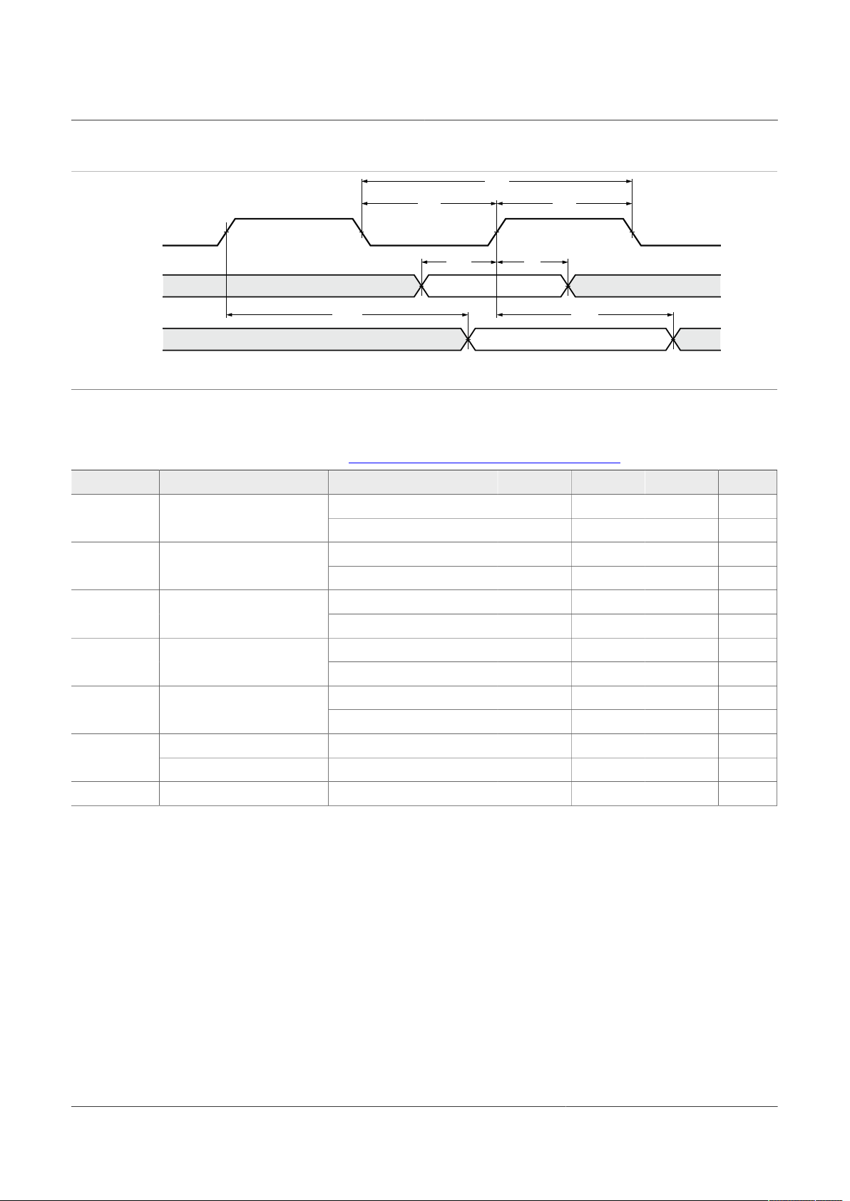
NXP Semiconductors
aaa- 036119
T
ISU
T
WL
T
WH
T
IH
Clock
Input
Output
T
ODLY
T
OH
f
PP
Dual-band 1x1 Wi-Fi 4 and Bluetooth 5.1 Combo SoC
Figure 14. SDIO protocol timing diagram—High-speed mode
IW416
Table 41. SDIO timing data—Default speed, high-speed modes
[1] , [2]
Unless otherwise specified, the values apply per Section 8 "Recommended operating conditions"
Symbol Parameter Condition Min Typ Max Unit
PP
Clock frequency
Normal 0 -- 25 MHzf
High-speed 0 -- 50 MHz
WL
Clock low time
Normal 10 -- -- nsT
High-speed 7 -- -- ns
WH
Clock high time
Normal 10 -- -- nsT
High-speed 7 -- -- ns
ISU
Input setup time
Normal 5 -- -- nsT
High-speed 6 -- -- ns
IH
Input hold time
Normal 5 -- -- nsT
High-speed 2 -- -- ns
ODLY
Output delay time Normal -- -- 14 nsT
CL ≤ 40 pF (1 card) High-speed -- -- 14 ns
T
OH
[1] For SDIO 2.0 running at 50 MHz clock frequency, VIO_SD must be 3.3V.
[2] For SDIO 2.0 running at 25 MHz clock frequency, VIO_SD must be 3.3V.
Output hold time High-speed 2.5 -- -- ns
IW416 All information provided in this document is subject to legal disclaimers. © NXP B.V. 2021. All rights reserved.
Preliminary data sheet Rev. 3 — 12 March 2021
61 / 97

NXP Semiconductors
aaa- 036120
T
IS
T
IH
T
CLK
T
CR
T
CF
Clock
Input
Output
T
ODLY
T
OH
f
PP
Dual-band 1x1 Wi-Fi 4 and Bluetooth 5.1 Combo SoC
9.7.3 SDR12, SDR25, SDR50 modes (up to 100 MHz) (1.8V)
Figure 15. SDIO protocol timing diagram—SDR12, SDR25, SDR50 modes (up to 100MHz) (1.8V)
Table 42. SDIO timing data——SDR12, SDR25, SDR50 modes (up to 100MHz) (1.8V)
Unless otherwise specified, the values apply per Section 8 "Recommended operating conditions"
IW416
Symbol Parameter Condition Min Typ Max Unit
f
PP
T
IS
T
IH
T
CLK
TCR, T
CF
Clock frequency SDR12/25/50 25 -- 100 MHz
Input setup time SDR12/25/50 3 -- -- ns
Input hold time SDR12/25/50 0.8 -- -- ns
Clock time SDR12/25/50 10 -- 40 ns
Rise time, fall time
SDR12/25/50 -- -- 0.2*T
CLK
ns
TCR, TCF < 2 ns (max) at
100 MHz
C
= 10 pF
CARD
T
ODLY
Output delay time
SDR12/25/50 -- -- 7.5 ns
CL ≤ 30 pF
T
OH
Output hold time
SDR12/25/50 1.5 -- -- ns
CL = 15 pF
IW416 All information provided in this document is subject to legal disclaimers. © NXP B.V. 2021. All rights reserved.
Preliminary data sheet Rev. 3 — 12 March 2021
62 / 97
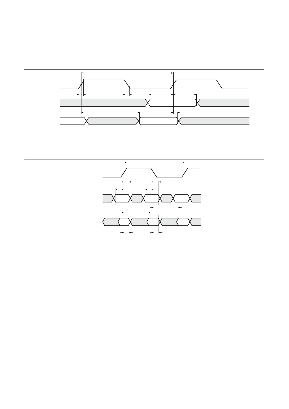
NXP Semiconductors
aaa- 036117
T
IS
T
IH
T
CLK
T
CR
T
CF
Clock
CMD Input
CMD Output
T
ODLY
T
OHLD
aaa- 036118
T
CLK
Clock
T
IH2x
T
IS2x
T
IH2x
T
IS2x
T
ODLY2x(max)
T
ODLY2x(max)
T
ODLY2x(min)
T
ODLY2x(min)
DAT[3:0]
Input
DAT[3:0]
Output
Dual-band 1x1 Wi-Fi 4 and Bluetooth 5.1 Combo SoC
9.7.4 DDR50 mode (50MHz) (1.8V)
Figure 16. SDIO CMD timing diagram—DDR50 mode (50MHz)
In DDR50 mode, DAT[3:0] lines are sampled on both edges of the clock (not applicable
for CMD line).
IW416
Figure 17. SDIO DAT[3:0] timing diagram—DDR50mode
IW416 All information provided in this document is subject to legal disclaimers. © NXP B.V. 2021. All rights reserved.
Preliminary data sheet Rev. 3 — 12 March 2021
63 / 97

NXP Semiconductors
IW416
Dual-band 1x1 Wi-Fi 4 and Bluetooth 5.1 Combo SoC
Table 43. SDIO timing data—DDR50 mode (50MHz)
Unless otherwise specified, the values apply per Section 8 "Recommended operating conditions"
Symbol Parameter Condition Min Typ Max Unit
Clock
T
CLK
TCR, T
CF
Clock Duty -- DDR50 45 -- 55 %
CMD Input (referenced to clock rising edge)
T
IS
T
IH
CMD Output (referenced to clock rising edge)
T
ODLY
T
OHLD
DAT[3:0] Input (referenced to clock rising and falling edges)
T
IS2x
T
IH2x
DAT[3:0] Output (referenced to clock rising and falling edges)
T
ODLY2x (max)
T
ODLY2x (min)
Clock time
50 MHz (max) between rising
edges
Rise time, fall time
TCR, TCF < 4.00 ns (max) at 50
MHz
C
= 10 pF
CARD
Input setup time
C
≤ 10 pF (1 card)
CARD
Input hold time
C
≤ 10 pF (1 card)
CARD
Output delay time during data
transfer mode
CL ≤ 30 pF (1 card)
Output hold time
CL ≥ 15 pF (1 card)
Input setup time
C
≤ 10 pF (1 card)
CARD
Input hold time
C
≤ 10 pF (1 card)
CARD
Output delay time during data
transfer mode
CL ≤ 25 pF (1 card)
Output hold time
CL ≥ 15 pF (1 card)
DDR50 20 -- -- ns
DDR50 -- -- 0.2*T
CLK
ns
DDR50 6 -- -- ns
DDR50 0.8 -- -- ns
DDR50 -- -- 13.7 ns
DDR50 1.5 -- -- ns
DDR50 3 -- -- ns
DDR50 0.8 -- -- ns
DDR50 -- -- 7.0 ns
DDR50 1.5 -- -- ns
9.7.5 SDIO internal pull-up/pull-down specifications
Table 44. SDIO internal pull-up/pull-down specifications
Unless otherwise specified, the values apply per Section 8 "Recommended operating conditions"
Parameter Condition Min Typ Max Unit
Internal nominal pull-up/pull-down
resistance
IW416 All information provided in this document is subject to legal disclaimers. © NXP B.V. 2021. All rights reserved.
Preliminary data sheet Rev. 3 — 12 March 2021
-- 60 90 120 kΩ
64 / 97
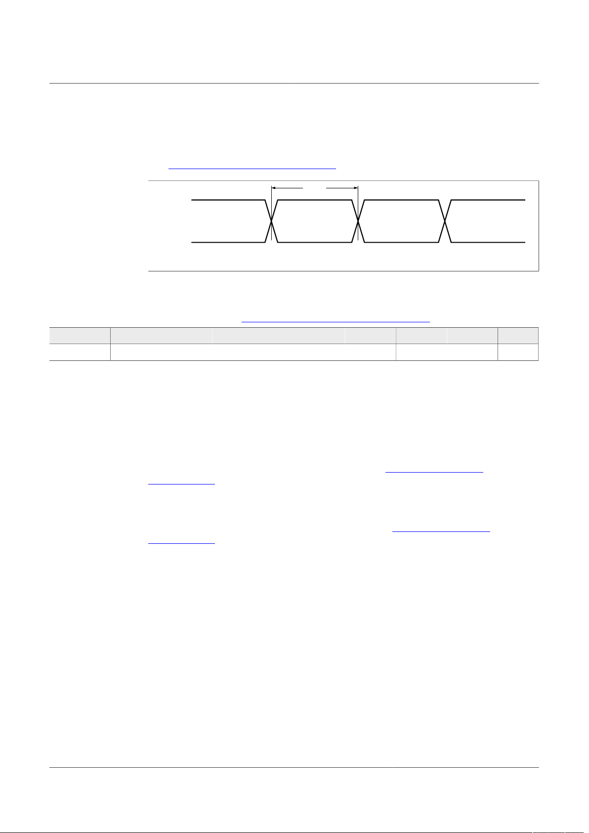
NXP Semiconductors
aaa- 036128
T
BAUD
UART Tx
UART Rx
9.8 High-speed UART specifications
The UART Tx and Rx pins are powered by VIO voltage supply.
See Section 9.1.1 "VIO DC characteristics" for DC specifications.
Figure 18. UART timing diagram
IW416
Dual-band 1x1 Wi-Fi 4 and Bluetooth 5.1 Combo SoC
Table 45. UART timing data
Unless otherwise specified, the values apply per Section 8 "Recommended operating conditions"
Symbol Parameter Condition Min Typ Max Units
T
BAUD
[1] The acceptable deviation from the UART Rx target baud rate is ±3%.
Baud rate 26 MHz or 40 MHz input clock 250 -- -- ns
[1]
9.9 Audio interface specifications
The device has two audio interfaces: I2S interface and PCM interface.
9.9.1 I2S interface specifications
The I2S pins are powered by VIO voltage supply. See Section 9.1.1 "VIO DC
characteristics" for the specifications.
9.9.2 PCM interface specifications
The PCM pins are powered by VIO voltage supply. See Section 9.1.1 "VIO DC
characteristics" for specifications.
IW416 All information provided in this document is subject to legal disclaimers. © NXP B.V. 2021. All rights reserved.
Preliminary data sheet Rev. 3 — 12 March 2021
65 / 97

NXP Semiconductors
Master Mode
PCM_CLK
PCM_DOUT
IW416
Dual-band 1x1 Wi-Fi 4 and Bluetooth 5.1 Combo SoC
T
BCLK
T
DO
PCM_DIN
T
DISU
T
DIHO
Figure 19. PCM timing specification diagram for data signals—Master mode
T
BCLKTBCLK
PCM_CLK
PCM_SYNC
T
BF
T
BF
Figure 20. PCM timing specification diagram for PCM_SYNC signal—Master mode
Table 46. PCM Timing Specification Data—Master Mode
Unless otherwise specified, the values apply per Section 8 "Recommended operating conditions"
Symbol Parameter Condition Min Typ Max Unit
F
BCLK
Duty Cycle
T
BCLK rise/fall
T
DO
Bit clock frequency -- -- 2/2.048 -- MHz
Bit clock duty cycle -- 0.4 0.5 0.6 --
BCLK
PCM_CLK rise/fall time -- -- 3 -- ns
Delay from PCM_CLK rising edge to
-- -- -- 15 ns
PCM_DOUT rising edge
T
DISU
Setup time for PCM_DIN before PCM_
-- 20 -- -- ns
CLK falling edge
T
DIHO
Hold time for PCM_DIN after PCM_CLK
-- 15 -- -- ns
falling edge
T
BF
Delay from PCM_CLK rising edge to
-- -- -- 15 ns
PCM_SYNC rising edge
IW416 All information provided in this document is subject to legal disclaimers. © NXP B.V. 2021. All rights reserved.
Preliminary data sheet Rev. 3 — 12 March 2021
66 / 97

NXP Semiconductors
Slave Mode
PCM_CLK
PCM_DOUT
IW416
Dual-band 1x1 Wi-Fi 4 and Bluetooth 5.1 Combo SoC
T
BCLK
T
DO
T
DIHO
PCM_DIN
T
DISU
Figure 21. PCM timing specification diagram for data signals—Slave mode
T
BCLK
PCM_CLK
PCM_SYNC
T
BFSU
T
BFHO
T
BF
Figure 22. PCM timing specification diagram for PCM_SYNC signal—Slave mode
Table 47. PCM timing specification data—Slave mode
Unless otherwise specified, the values apply per Section 8 "Recommended operating conditions"
Symbol Parameter Condition Min Typ Max Unit
F
BCLK
Duty Cycle
T
BCLK rise/fall
T
DO
Bit clock frequency -- -- 2/2.048 -- MHz
Bit clock duty cycle -- 0.4 0.5 0.6 --
BCLK
PCM_CLK rise/fall time -- -- 3 -- ns
Delay from PCM_CLK rising edge to
-- -- -- 30 ns
PCM_DOUT rising edge
T
DISU
Setup time for PCM_DIN before PCM_
-- 15 -- -- ns
CLK falling edge
T
DIHO
Hold time for PCM_DIN after PCM_CLK
-- 10 -- -- ns
falling edge
T
BFSU
Setup time for PCM_SYNC before
-- 15 -- -- ns
PCM_CLK falling edge
T
BFHO
Hold time for PCM_SYNC after PCM_
-- 10 -- -- ns
CLK falling edge
IW416 All information provided in this document is subject to legal disclaimers. © NXP B.V. 2021. All rights reserved.
Preliminary data sheet Rev. 3 — 12 March 2021
67 / 97
NXP Semiconductors
IW416
Dual-band 1x1 Wi-Fi 4 and Bluetooth 5.1 Combo SoC
9.10 Reference clock specifications
9.10.1 External crystal oscillator specifications
Note: The reference clock from the external crystal oscillator requires a CMOS input
signal.
Table 48. Clock DC specifications
Unless otherwise specified, the values apply per Section 8 "Recommended operating conditions"
Parameter Condition Min Typ Max Unit
Single-ended high-level voltage -- -- -- 1.8 V
Single-ended low-level voltage -- 0 -- -- V
Clock amplitude (pk-pk) -- 0.5 -- 1 V
Mid-point slope -- 125 -- -- MV/s
[1] AC-coupling capacitor is integrated into the SoC.
[1]
Table 49. 26 MHz clock timing
Unless otherwise specified, the values apply per Section 8 "Recommended operating conditions"
Parameter Condition Min Typ Max Unit
XO26 period -- 38.46 -
20 ppm
XO26 rise time -- -- -- 5.00 ns
XO26 fall time -- -- -- 5.00 ns
XO26 duty cycle -- 48.05 50 51.95 %
Table 50. 40 MHz clock timing
Unless otherwise specified, the values apply per Section 8 "Recommended operating conditions"
Parameter Condition Min Typ Max Unit
XO40 period -- 25.00 -
20 ppm
XO40 rise time -- -- -- 2.00 ns
XO40 fall time -- -- -- 2.00 ns
XO40 duty cycle -- 47 50 53 %
38.46 38.46 +
20 ppm
25.00 25.00 +
20 ppm
ns
ns
IW416 All information provided in this document is subject to legal disclaimers. © NXP B.V. 2021. All rights reserved.
Preliminary data sheet Rev. 3 — 12 March 2021
68 / 97

NXP Semiconductors
IW416
Dual-band 1x1 Wi-Fi 4 and Bluetooth 5.1 Combo SoC
Table 51. Phase noise—2.4 GHz operation
Unless otherwise specified, the values apply per Section 8 "Recommended operating conditions"
Parameter Condition Min Typ Max Unit
Fref = 26 MHz
Fref = 40 MHz
Table 52. Phase noise—5 GHz operation
Unless otherwise specified, the values apply per Section 8 "Recommended operating conditions"
Offset = 1 kHz -- -- -126 dBc/Hz
Offset = 10 kHz -- -- -137 dBc/Hz
Offset = 100 kHz -- -- -145 dBc/Hz
Offset > 1 MHz -- -- -145 dBc/Hz
Offset = 1 kHz -- -- -126 dBc/Hz
Offset = 10 kHz -- -- -137 dBc/Hz
Offset = 100 kHz -- -- -145 dBc/Hz
Offset > 1 MHz -- -- -145 dBc/Hz
Parameter Test Conditions Min Typ Max Unit
Fref = 26 MHz
Fref = 40 MHz
Offset = 1 kHz -- -- -130 dBc/Hz
Offset = 10 kHz -- -- -150 dBc/Hz
Offset = 100 kHz -- -- -156 dBc/Hz
Offset > 1 MHz -- -- -156 dBc/Hz
Offset = 1 kHz -- -- -130 dBc/Hz
Offset = 10 kHz -- -- -150 dBc/Hz
Offset = 100 kHz -- -- -156 dBc/Hz
Offset > 1 MHz -- -- -156 dBc/Hz
IW416 All information provided in this document is subject to legal disclaimers. © NXP B.V. 2021. All rights reserved.
Preliminary data sheet Rev. 3 — 12 March 2021
69 / 97

NXP Semiconductors
IW416
Dual-band 1x1 Wi-Fi 4 and Bluetooth 5.1 Combo SoC
9.10.2 External crystal specifications
Table 53. External crystal specifications
Unless otherwise specified, the values apply per Section 8 "Recommended operating conditions"
Parameter Condition Min Typ Max Unit
Fundamental frequencies -- -- 26 (40) -- MHz
Resonance mode -- -- A1,
Fundamental
Equivalent differential load
capacitance
Shunt capacitance -- -- 2 -- pF
Frequency tolerance Over process at 25ºC -- ±10 -- ppm
Frequency stability Over operating temperature -- ±10 -- ppm
Aging -- -- ±2 -- ppm/5
Insulation resistance at DC 100V 500 -- -- MΩ
Drive level -- 150 -- -- µW
-- -- 5 -- pF
26 MHz -- -- 60 ΩSeries resistance (ESR)
40 MHz -- -- 60 Ω
-- --
years
9.10.3 External sleep clock specifications
Table 54. External sleep clock specifications
Unless otherwise specified, the values apply per Section 8 "Recommended operating conditions"
Parameter Min Typ Max Unit
Clock frequency range/accuracy
• CMOS input clock signal type
• ±250 ppm (initial, aging, temperature)
Phase noise requirement (@ 100 kHz) -- -125 -- dBc/Hz
Cycle jitter -- 1.5 -- ns (RMS)
Slew rate limit (10-90%) -- -- 100 ns
Duty cycle tolerance 20 -- 80 %
[1] Voltage input level = 1.8V. See Section 9.1.1 "VIO DC characteristics".
[1]
-- 32.768 -- kHz
IW416 All information provided in this document is subject to legal disclaimers. © NXP B.V. 2021. All rights reserved.
Preliminary data sheet Rev. 3 — 12 March 2021
70 / 97

NXP Semiconductors
aaa- 036126
T
RPW
T
PU_RESET
PDn
Power
Dual-band 1x1 Wi-Fi 4 and Bluetooth 5.1 Combo SoC
9.11 Power down (PDn) pin specifications
9.11.1 PDn asserted low—All power supplies good
Figure 23 and Table 55 show the specifications for the PDn signal when it is asserted
(low) while all power supplies to the device are good.
Figure 23. PDn pin (Power-down) timing—Power remains high at PDn assertion
Table 55. PDn pin (Power Down) specifications—Power remains high at PDn assertion
Unless otherwise specified, the values apply per Section 8 "Recommended operating conditions"
IW416
Symbol Parameter Condition Min Typ Max Unit
T
PU_RESET
Valid power to PDn de-
-- 0 -- -- ms
asserted
T
RPW
V
IH
V
IL
[1] Minimum value guaranteed for a valid reset. Smaller values may put the device in an undefined state.
PDn pulse width -- 1
Input high voltage -- 1.4 -- 4.5 V
Input low voltage -- -0.4 -- 0.5 V
[1]
-- -- µs
IW416 All information provided in this document is subject to legal disclaimers. © NXP B.V. 2021. All rights reserved.
Preliminary data sheet Rev. 3 — 12 March 2021
71 / 97

NXP Semiconductors
aaa- 036125
TRD = time from PDn asser tion until power supply drops to 0.2 V
T
RD
0.2 V
T
RPW
T
PU_RESET
PDn
Power
Dual-band 1x1 Wi-Fi 4 and Bluetooth 5.1 Combo SoC
9.11.2 PDn asserted low—One or more power supplies ramp down
Figure 24 and Table 56 show the specifications for the PDn signal when it is asserted
(low) while 1 or more of the power supplies (including VCORE) ramps down. When the
integrated LDO is used, VCORE will ramp down when PDn is asserted.
Figure 24. PDn pin (Power Down) timing—Power ramps down at PDn assertion
Table 56. PDn pin (Power Down) specifications—Power ramps down at PDn assertion
Unless otherwise specified, the values apply per Section 8 "Recommended operating conditions"
IW416
Symbol Parameter Condition Min Typ Max Unit
T
PU_RESET
Valid power to PDn de-
-- 0 -- -- ms
asserted
T
RPW
V
IH
V
IL
[1] Minimum value guaranteed for a valid reset. Smaller values may put the device in an undefined state.
PDn pulse width -- TRD
Input high voltage -- 1.4 -- 4.5 V
Input low voltage -- -0.4 -- 0.2 V
[1]
-- -- µs
IW416 All information provided in this document is subject to legal disclaimers. © NXP B.V. 2021. All rights reserved.
Preliminary data sheet Rev. 3 — 12 March 2021
72 / 97

NXP Semiconductors
aaa- 036123
JTAG_TCK
T
SU_TDI
T
L_TCK
T
P_TCK
T
H_TCK
T
DLY_TDO
T
HD_TDI
JTAG_TDO
JTAG_TDI
JTAG_TMS
IW416
Dual-band 1x1 Wi-Fi 4 and Bluetooth 5.1 Combo SoC
9.12 Configuration pin specifications
For a list of configuration pins, see Section 5.6 "Configuration pins".
Table 57. Configuration pin specifications
Unless otherwise specified, the values apply per Section 8 "Recommended operating conditions"
Parameter Condition Min Typ Max Unit
Internal weak pull-up resistance Around 1 ms following any reset -- 800 -- kΩ
Internal nominal pull-up resistance Around 1 ms following any reset -- 100 -- kΩ
[1] After approximately 1 ms, the configuration pins become functional pins.
[1]
9.13 JTAG interface specifications
JTAG interface pins are powered by VIO voltage supply.
See Section 9.1.1 "VIO DC characteristics" for specifications.
Figure 25. JTAG timing diagram
Table 58. JTAG timing data
[1]
Unless otherwise specified, the values apply per Section 8 "Recommended operating conditions"
Symbol Parameter Condition Min Typ Max Unit
T
P_TCK
T
H_TCK
T
L_TCK
T
SU_TDI
T
HD_TDI
T
DLY_TDO
[1] Does not apply to JTAG enabled by the JTAG_TMS pin.
IW416 All information provided in this document is subject to legal disclaimers. © NXP B.V. 2021. All rights reserved.
Preliminary data sheet Rev. 3 — 12 March 2021
TCK period -- 40 -- -- ns
TCK high -- 12 -- -- ns
TCK low -- 12 -- -- ns
TDI, TMS to TCK setup time -- 10 -- -- ns
TDI, TMS to TCK hold time -- 10 -- -- ns
TCK to TDO delay -- 0 -- 15 ns
73 / 97
NXP Semiconductors
IW416
Dual-band 1x1 Wi-Fi 4 and Bluetooth 5.1 Combo SoC
10 Package information
10.1 Package thermal conditions
10.1.1 68-pin HVQFN thermal conditions
Table 59. Package thermal conditions—HVQFN
Symbol Parameter Condition Typ Units
θ
JA
Thermal resistance
Junction to ambient of package.
θJA = (TJ - TA)/ P
P = total power dissipation
JEDEC 3 in. x 4.5 in.
4-layer PCB
no air flow
JEDEC 3 in. x 4.5 in.
4-layer PCB
1 meter/sec air flow
JEDEC 3 in. x 4.5 in.
4-layer PCB
2 meter/sec air flow
JEDEC 3 in. x 4.5 in.
4-layer PCB
3 meter/sec air flow
ψ
JT
ψ
JB
Thermal characteristic parameter
Junction to top-center of package.
ψJT = (TJ - T
T
= temperature on top-center of package
TOP
TOP
)/P
Thermal characteristic parameter
Junction to bottom surface, center of PCB.
ψJB = (TJ - TB)/P
JEDEC 3 in. x 4.5 in.
4-layer PCB
no air flow
JEDEC 3 in. x 4.5 in.
4-layer PCB
no air flow
TB = surface temperature of PCB
θ
JC
Thermal resistance
Junction to case of the package.
θJC = (TJ - TC)/ P
TOP
JEDEC 3 in. x 4.5 in.
4-layer PCB
no air flow
TC = temperature on top-center of package
P
= power dissipation from top of package
TOP
θ
JB
Thermal resistance
Junction to board of package.
θJB = (TJ - TB)/ P
P
= power dissipation from bottom of package to PCB
BOTTOM
BOTTOM
JEDEC 3 in. x 4.5 in.
4-layer PCB
no air flow
surface
28.4 °C/W
27.6 °C/W
26.1 °C/W
25.3 °C/W
0.44 °C/W
15.4 °C/W
13.0 °C/W
15.6 °C/W
IW416 All information provided in this document is subject to legal disclaimers. © NXP B.V. 2021. All rights reserved.
Preliminary data sheet Rev. 3 — 12 March 2021
74 / 97

NXP Semiconductors
10.1.2 76-bump WLCSP thermal conditions
IW416
Dual-band 1x1 Wi-Fi 4 and Bluetooth 5.1 Combo SoC
Table 60. Package thermal conditions—WLCSP
Symbol Parameter Board type
θ
JA
Junction to ambient thermal resistance
[2]
JESD51-9, 2s2p 37.6 °C/W
[1]
Typ Units
θJA = (TJ - TA)/ P
P = total power dissipation
ψ
JT
[1] The thermal test board meets JEDEC specification for this package (JESD51-9).
[2] Determined in accordance to JEDEC JESD51-2A natural convection environment. Thermal resistance data in this report is solely for a thermal
performance comparison of one package to another in a standardized specified environment. It is not meant to predict the performance of a package in an
application-specific environment.
Junction to top of package thermal characterization parameter
ψJT = (TJ - T
T
= temperature on top-center of package
TOP
TOP
)/P
[2]
JESD51-9, 2s2p 1.3 °C/W
IW416 All information provided in this document is subject to legal disclaimers. © NXP B.V. 2021. All rights reserved.
Preliminary data sheet Rev. 3 — 12 March 2021
75 / 97

NXP Semiconductors
10.2 Package mechanical drawing
10.2.1 68-pin HVQFN mechanical drawing
IW416
Dual-band 1x1 Wi-Fi 4 and Bluetooth 5.1 Combo SoC
Figure 26. 68-pin HVQFN package mechanical drawing
IW416 All information provided in this document is subject to legal disclaimers. © NXP B.V. 2021. All rights reserved.
Preliminary data sheet Rev. 3 — 12 March 2021
76 / 97
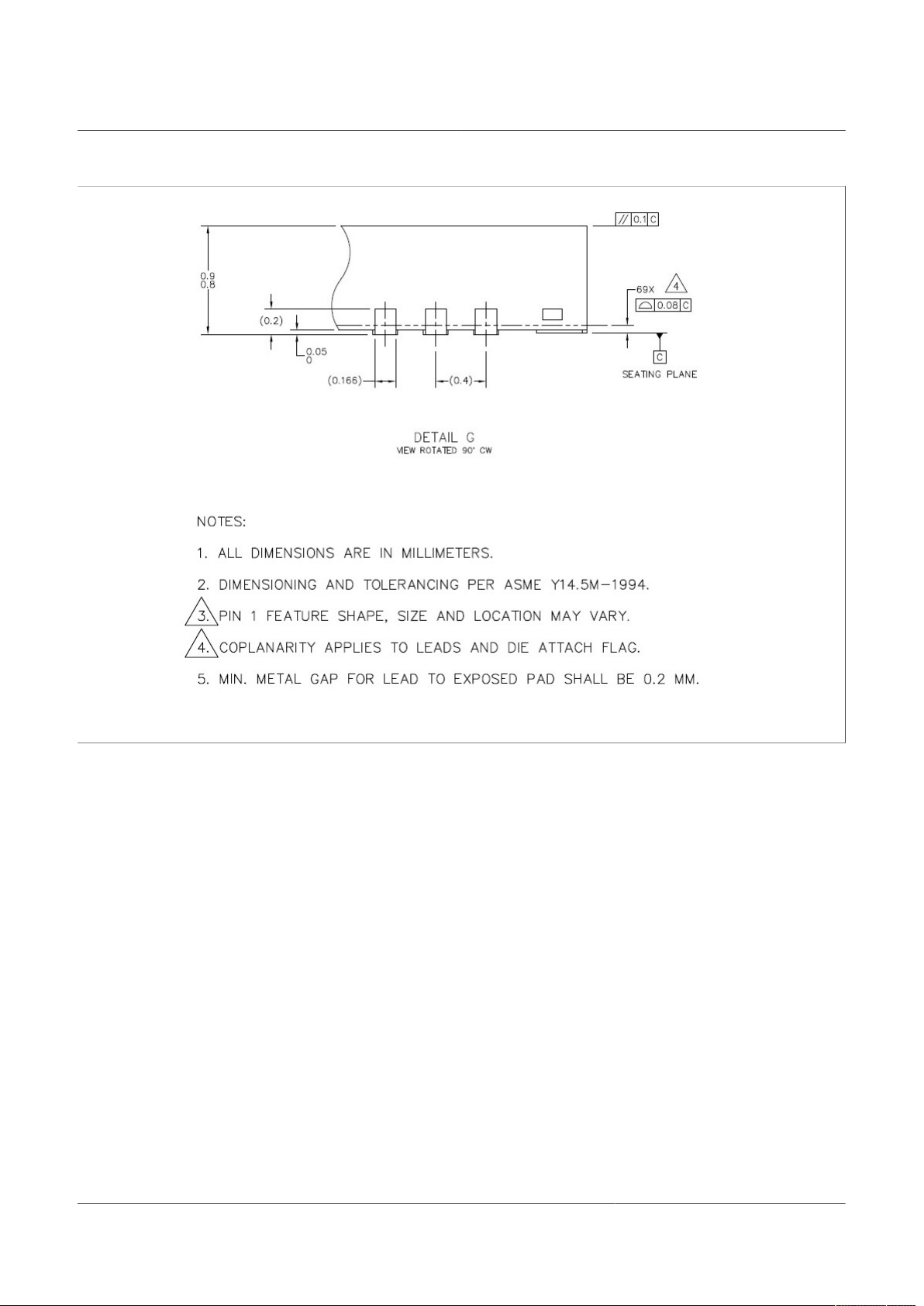
NXP Semiconductors
IW416
Dual-band 1x1 Wi-Fi 4 and Bluetooth 5.1 Combo SoC
Figure 27. 68-pin HVFQN package mechanical drawing - Detail G
IW416 All information provided in this document is subject to legal disclaimers. © NXP B.V. 2021. All rights reserved.
Preliminary data sheet Rev. 3 — 12 March 2021
77 / 97
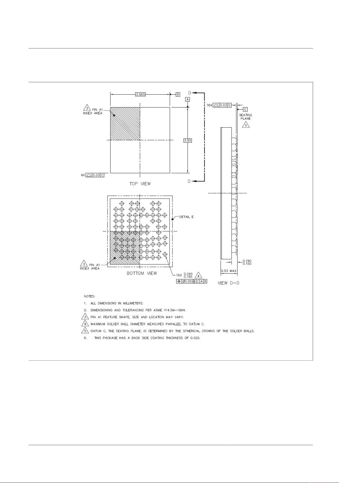
NXP Semiconductors
10.2.2 76-bump WLCSP mechanical drawing
IW416
Dual-band 1x1 Wi-Fi 4 and Bluetooth 5.1 Combo SoC
Backside coating included
Figure 28. 76-bump WLCSP package mechanical drawing
IW416 All information provided in this document is subject to legal disclaimers. © NXP B.V. 2021. All rights reserved.
Preliminary data sheet Rev. 3 — 12 March 2021
78 / 97
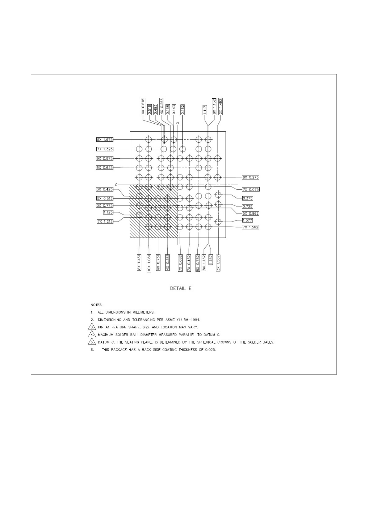
NXP Semiconductors
IW416
Dual-band 1x1 Wi-Fi 4 and Bluetooth 5.1 Combo SoC
Backside coating included
Figure 29. 76-bump WLCSP package mechanical drawing - Detail E
IW416 All information provided in this document is subject to legal disclaimers. © NXP B.V. 2021. All rights reserved.
Preliminary data sheet Rev. 3 — 12 March 2021
79 / 97
NXP Semiconductors
10.3 Package marking
10.3.1 68-pin HVFQN marking
Figure 30 and Figure 31 show the location of pin 1 and describe each line of the package
marking on 68-pin HVQFN.
Pin 1 location
IW416
Dual-band 1x1 Wi-Fi 4 and Bluetooth 5.1 Combo SoC
JE = Foundry
A = Assembly center
D = RoHS
YYWW = Date code
(YY = year - WW = week)
X = used for engineering samples
Note: The above drawing is not drawn to scale. The location of markings is approximate.
IW416HNA1C
XXXXX.%%
JEADYYWWX
IW416 = Part number
HN = Package code
A1 = Die version
C = Commercial operating temperature range
XXXXX = Diffusion lot number - dot - %% = ASID number
Figure 30. Package marking and pin 1 location—68-pin HVQFN, commercial operating temperature
Pin 1 location
JE = Foundry
A = Assembly center
D = RoHS
YYWW = Date code
(YY = year - WW = week)
X = used for engineering samples
IW416HNA1I
XXXXX.%%
JEADYYWWX
IW416 = Part number
HN = Package code
A1 = Die version
I = industrial operating temperature range
XXXXX = Diffusion lot number - dot - %% = ASID number
Note: The above drawing is not drawn to scale. The location of markings is approximate.
Figure 31. Package marking and pin 1 location—68-pin HVQFN, industrial operating temperature
IW416 All information provided in this document is subject to legal disclaimers. © NXP B.V. 2021. All rights reserved.
Preliminary data sheet Rev. 3 — 12 March 2021
80 / 97

NXP Semiconductors
10.3.2 76-bump WLCSP marking
Figure 32 and Figure 33 show the location of pin 1 and describes each line of the
package marking on the 76-bump WLCSP.
Pin 1 location
IW416
Dual-band 1x1 Wi-Fi 4 and Bluetooth 5.1 Combo SoC
IW416 = Part number - HN = Package code - A1 = Die version
C = Commercial operating temperature range
XY die coordinates
NXP (fixed)
X: engineering samples
Note: The above drawing is not drawn to scale. The location of markings is approximate.
IW416UKA1C
XXXXX.%%
JEkDYYWW
XXX-YYY
NXP X
XXXXX = Diffusion lot # - %% = wafer number
JE = Foundry
k = Bumping center
D = RoHS
YYWW = date code – YY = year – WW = week
Figure 32. Package marking and pin 1 location—76-bump WLCSP, commercial operating temperature range
Pin 1 location
IW416 = Part number - HN = Package code - A1 = Die version
I = Industrial operating temperature range
XY die coordinates
NXP (fixed)
X: engineering samples
IW416UKA1I
XXXXX.%%
JEkDYYWW
XXX-YYY
NXP X
XXXXX = Diffusion lot # - %% = wafer number
JE = Foundry
k = Bumping center
D = RoHS
YYWW = date code – YY = year – WW = week
Note: The above drawing is not drawn to scale. The location of markings is approximate.
Figure 33. Package marking and pin 1 location—76-bump WLCSP, industrial operating temperature range
IW416 All information provided in this document is subject to legal disclaimers. © NXP B.V. 2021. All rights reserved.
Preliminary data sheet Rev. 3 — 12 March 2021
81 / 97

NXP Semiconductors
11 Acronyms and abbreviations
Table 61. Acronyms and abbreviations
Acronym Definition
A2DP Advanced audio distribution profiles
ABR Automatic baud rate
ACK Acknowledgment
ADAS Advanced driver assistance systems
ADC Analog-to-digital converter
AES Advanced encryption standard
AFC Automatic frequency correction
AFH Adaptive frequency hopping
AGC Automatic gain control
AIFS Arbitration inter-frame space
AoA Angle of arrival
AoD Angle of departure
AP Access point
APB Advanced peripheral bus
API Application program interface
aQFN Advanced quad flat non-leaded package
ARM Advanced RISC machine
ATIM Announcement traffic indication message
BAMR Base address mask register
BAR Base address register
BBU Baseband processor unit
BCB Benzocyclobutene (flip chip bump process)
BDR Basic data rate
BER Bit error rate
BOM Bill of materials
BR Baud rate
BRF Bluetooth RF unit
BSS Basic service set
BSSID Basic service set identifier
BTM BSS transition management
BTU Bluetooth baseband unit
BWQ Bandwidth queue
CBC Cipher block chaining
CBP Contention-based period
IW416
Dual-band 1x1 Wi-Fi 4 and Bluetooth 5.1 Combo SoC
IW416 All information provided in this document is subject to legal disclaimers. © NXP B.V. 2021. All rights reserved.
Preliminary data sheet Rev. 3 — 12 March 2021
82 / 97

NXP Semiconductors
Table 61. Acronyms and abbreviations...continued
Acronym Definition
CCA Clear channel assessment
CCK Complementary code keying
CCMP Counter mode CBC-MAC protocol
CDE Close descriptor enable
CFP Contention-free period
CFQ Contention-free queue
CID Connection identifier
CIS Card information structure
CIU CPU interface unit
CMD Command
CMQ Control management queue
CRC Cyclic redundancy check
CS Card select
CSL Coordinated sampled listening
CSMA/CA Carrier sense multiple access / collision avoidance
CSMA/CD Carrier sense multiple access / collision detection
CSU Clocked serial unit
CTS Clear to send
DAC Digital-to-analog converter
DBPSK Differential binary phase shift keying
DCD Device controller driver
DCE Data communication equipment
DCF Distributed coordination function
DCLA Direct current level adjustment
DCLB Digital contactless bridge
DCU DMA controller unit
DFS Dynamic frequency selection
DIFS Distributed inter frame space
DMA Direct memory access
dQH Device queue head
DQPSK Differential quadrature phase shift keying
DSM Distribution system medium
DSP Digital signal processor
DSRC Dedicated short range communications
dTD Linked list transfer descriptors
DTIM Delivery traffic indication message
IW416
Dual-band 1x1 Wi-Fi 4 and Bluetooth 5.1 Combo SoC
IW416 All information provided in this document is subject to legal disclaimers. © NXP B.V. 2021. All rights reserved.
Preliminary data sheet Rev. 3 — 12 March 2021
83 / 97

NXP Semiconductors
Table 61. Acronyms and abbreviations...continued
Acronym Definition
DUP Duplicated packet
DVSC Digital voltage scaling control
EAP Extensible authentication protocol
EBRAM Extended block random access memory
ECDSA Elliptic curve digital signature algorithm
ED Energy detect
EDCA Enhanced distributed channel access
EEPROM Electrically erasable programmable read only memory
EIFS Extended inter frame Space
EMC Electromagnetic compatibility
ER Extended range
ERP-OFDM Extended rate PHY-orthogonal frequency division multiplexing
ETSI European telecommunications standards institute
eWLP Embedded wafer level package
FAE Field application engineer
FCC Federal communications commission
FIFO First in first out
FIPS Federal information processing standards
FIQ Fast interrupt request
FW Firmware
GATT Generic attribute profile
GCMP Galois/counter mode protocol
GI Guard interval
GPIO General purpose input/output
GPL General Public License
GPU General purpose input/output unit
HID Human interface device
HIU Host interface unit
HOGP HID over GATT profile
HSP Hands-free profile
HT High throughput
HW Hardware
I/F Interface
I/Q In-phase/quadrature
IB In band
IBSS Independent basic service set
IW416
Dual-band 1x1 Wi-Fi 4 and Bluetooth 5.1 Combo SoC
IW416 All information provided in this document is subject to legal disclaimers. © NXP B.V. 2021. All rights reserved.
Preliminary data sheet Rev. 3 — 12 March 2021
84 / 97

NXP Semiconductors
Table 61. Acronyms and abbreviations...continued
Acronym Definition
ICE In-circuit emulator (or emulation)
ICR Interrupt cause register
ICU Interrupt controller unit
ICV Integrity check value
IE Information element
IEEE Institute of electrical and electronics engineers
IEMR Interrupt event mask register
IFS inter frame space
IMR Interrupt mask register
IPG Inter-packet gap
IPsec Internet protocol security
IR Infrared
IRQ Interrupt request
ISA Instruction set architecture
ISDN Integrated services digital network
ISM Industrial, scientific, and medical
ISMR Interrupt status mask register
ISR Interrupt status register
JEDEC Joint electronic device engineering council
JTAG Joint test action group
LC3 Low complexity communication codec
LDPC Low density parity check
LE Low energy
LED Light emitting diode
LME Layer management entity
LNA Low noise amplifier
LPM Low power management
LQFN Low quad flat non-leaded
LSb Least significant bit
LSB Least significant byte
LSP Low-speed peripheral
LTE Long term evolution
MAC Media/medium access controller
MC Memory controller
MCS Modulation and coding scheme
MCU MAC Control unit
IW416
Dual-band 1x1 Wi-Fi 4 and Bluetooth 5.1 Combo SoC
IW416 All information provided in this document is subject to legal disclaimers. © NXP B.V. 2021. All rights reserved.
Preliminary data sheet Rev. 3 — 12 March 2021
85 / 97

NXP Semiconductors
Table 61. Acronyms and abbreviations...continued
Acronym Definition
MDI Modem data interface
MIB Management information base
MIC Message integrity code
MII Media independent interface
MIMO Multiple input multiple output
MIPS Million instructions per second
MLME MAC sublayer management entity
MMI Modem management interface
MMPDU MAC management protocol data unit
MMU Memory management unit
MPDU MAC protocol data unit
MSb Most significant bit
MSB Most significant byte
MSDU MAC service data unit
MU-MIMO Multi user MIMO
MU-PPDU Multi user PPDU
MWS Mobile wireless system
NAV Network allocation vector
NBS Narrow band speech
NDP Null data packet
NL No load
NPTR Next descriptor pointer
Nsts Number of space time streams
OCB Outside the context of a BSS
OFDM Orthogonal frequency division multiplexing
OID Object identifier
OOB Out of band
OTP One time programmable
P2P Peer-to-peer
PA Power amplifier
PAD Packet assembler/disassembler
PBU Peripheral bus unit
PC Point coordinator
PCB Printed circuit board
PCF Point coordination function
IW416
Dual-band 1x1 Wi-Fi 4 and Bluetooth 5.1 Combo SoC
Multimedia wireless system
IW416 All information provided in this document is subject to legal disclaimers. © NXP B.V. 2021. All rights reserved.
Preliminary data sheet Rev. 3 — 12 March 2021
86 / 97

NXP Semiconductors
Table 61. Acronyms and abbreviations...continued
Acronym Definition
PCI Peripheral component interconnect
PCIe PCI express
PCM Pulse code modulation
PDn Power down
PDU Protocol data unit
PEAP Protected EAP
PHY Physical layer
PIFS Priority inter frame space
PLL Phase-locked loop
PLME Physical layer management entity
PMU Power management unit
POS Point of sale
POST Power-on self test
PPDU PHY protocol data unit
PPK Per-packet key
PPM Pulse position modulation
PSK Pre shared keys
PTA Packet traffic arbitration
PUF Physically unclonable function
PWK Pairwise key
QAM Quadrature amplitude modulation
QFN Quad flat non-leaded package
QoS Quality of service
RA Receiver address
RBDS Radio broadcast data system
RDS Radio data system
RF Radio frequency
RFID Radio frequency identification
RIFS Reduced inter frame space
RISC Reduced instruction set computer
ROM Read only memory
RSSI Receiver signal strength indication
RTC Real time clock
RTS Request to send
RTU General purpose timer unit
RU Resource unit
IW416
Dual-band 1x1 Wi-Fi 4 and Bluetooth 5.1 Combo SoC
IW416 All information provided in this document is subject to legal disclaimers. © NXP B.V. 2021. All rights reserved.
Preliminary data sheet Rev. 3 — 12 March 2021
87 / 97

NXP Semiconductors
Table 61. Acronyms and abbreviations...continued
Acronym Definition
SA Source address
SAP Service access point
SCLK Serial interface clock
SDA Serial interface data
SDK Software development kit
SE Secure element
SFD Start of frame delimiter
SHA Secure hash algorithm
SIFS Short inter frame space
SISO Single input single output
SIU Serial interface unit (UART)
SJU System/software JTAG controller unit
SM Switch module
SMI Serial management interface
SNR Signal-to-noise ratio
SO Serial out
SoC System-on-chip
SPDT Single pole double throw
SPI Serial peripheral interface
SQU Internal SRAM unit
SRWB Serial interface read write
SS Service set
SSID Service set identifier
STA Station
STBC Space-time block code
SWD Serial wire debug
SWP Single wire protocol
TA Transmitter address
TBG Time base generator
TBTT Target beacon transmission time
TCM Tightly coupled memory
TCP/IP Transmission control protocol/internet protocol
TCQ Traffic category queue
TEE Trusted execution environment
TIM Traffic indication map
TKIP Temporal key integrity protocol
IW416
Dual-band 1x1 Wi-Fi 4 and Bluetooth 5.1 Combo SoC
IW416 All information provided in this document is subject to legal disclaimers. © NXP B.V. 2021. All rights reserved.
Preliminary data sheet Rev. 3 — 12 March 2021
88 / 97

NXP Semiconductors
Table 61. Acronyms and abbreviations...continued
Acronym Definition
TPC Transmit power control
TQFP Thin quad flat pack
TRPC Transmit rate-based power control
TSC TKIP sequence counter
TSF Timing synchronization function
TWT Target wait time
UART Universal asynchronous receiver/transmitter
UBM Under bump metal
UDP User datagram protocol
UNII Unlicensed national information infrastructure
VCO Voltage controlled oscillator
VHT Very high throughput
VIF Voice interface
WAP Wireless application protocol
WAVE Wireless access in vehicular environments
WBS Wide band speech
WCI-2 Wireless coexistence interface 2
WEP Wired equivalent privacy
WI Wired interface
Wi-Fi Hardware implementation of IEEE 802.11 for wireless connectivity
WLAN Wireless local area network
WMM Wi-Fi multimedia
WPA Wi-Fi protected access
WPA2 Wi-Fi protected access 2
WPA2-PSK Wi-Fi protected access 2 - pre shared key
WPA3 Wi-Fi protected access 3
WPA-PSK Wi-Fi protected access - pre shared key
XFQFN Extra-fine quad flat non-leaded
XIP Execute in place
XOSC Crystal oscillator
ZIF Zero intermediate frequency
IW416
Dual-band 1x1 Wi-Fi 4 and Bluetooth 5.1 Combo SoC
IW416 All information provided in this document is subject to legal disclaimers. © NXP B.V. 2021. All rights reserved.
Preliminary data sheet Rev. 3 — 12 March 2021
89 / 97
NXP Semiconductors
Dual-band 1x1 Wi-Fi 4 and Bluetooth 5.1 Combo SoC
12 Revision history
IW416 v.3.0 20210312 Preliminary data sheet - IW416 v.2.0
Modifications
Product overview
• Section 1 "Product overview": updated
• Section 1.2 "Wi-Fi key features": updated
• Section 1.3 "Bluetooth key features": updated
• Section 1.4 "Host interfaces": updated
Ordering information
• Figure 3 "Part numbering scheme": updated
• Table 1 "Part order codes": updated
Wi-Fi subsystem
• Section 3.1 "IEEE 802.11 standards": updated
• Section 3.3 "Wi-Fi baseband": updated
• Section 3.6 "Wi-Fi host interfaces": updated
Bluetooth subsystem
• Section 4.3 "Bluetooth host interfaces": updated
• Section 4.5 "Coexistence": updated
Pin information
• Section 5.4 "Pin types": added A I/O
• Section 5.5.1 "Pin states": updated
• Section 5.5.2 "General purpose I/O (GPIO) (MFP)": updated GPIO[15], GPIO[14],
GPIO[13], GPIO[12], GPIO[5] , GPIO[4], and GPIO[1] description
• Section 5.5.10 "Clock interface": updated XTAL_IN and SLP_CLK_IN descriptions
• Section 5.5.12 "Power supply and ground": updated VIO_SD description
• Section 5.5.13 "JTAG interface": added
• Section 5.6 "Configuration pins": updated the second table Host configuration options
Power information
• Section 6.1 "Power modes": added a table footnote for deep-sleep mode
• Section 6.2 "Power-up sequence": updated the introduction
• Section 6.3 "Power-down sequence": updated VCORE value in the figure
• Section 6.3.2 "Host power-down pin (PMIC_EN) usage": updated VCORE value in the
figure
Absolute maximum ratings
• Table 24 "Absolute maximum ratings ": updated the parameter definitions and removed the
column with typical values. No change for the min. and max. values.
Electrical specifications
• Section 9.10.2 "External crystal specifications": updated the series resistance (ESR)
maximum value
• Section 9.3.1 "Wi-Fi radio performance measurement": added
• Section 9.3.2 "2.4 GHz Wi-Fi receive performance": updated
• Section 9.3.3 "5 GHz receive performance": updated
• Section 9.3.4 "2.4 GHz transmit performance": updated
• Section 9.3.4 "2.4 GHz transmit performance": updated
• Section 9.4.1 "Bluetooth/Bluetooth LE receive performance": updated
• Section 9.4.2 "Bluetooth/Bluetooth LE transmit performance": updated
• Section 9.6 "Current consumption": updated
Package information
• Section 10.1.2 "76-bump WLCSP thermal conditions": added
• Section 10.3.1 "68-pin HVFQN marking": updated
• Section 10.3.2 "76-bump WLCSP marking": added
IW416
IW416 All information provided in this document is subject to legal disclaimers. © NXP B.V. 2021. All rights reserved.
Preliminary data sheet Rev. 3 — 12 March 2021
90 / 97

NXP Semiconductors
Dual-band 1x1 Wi-Fi 4 and Bluetooth 5.1 Combo SoC
Table 62. Revision history...continued
Document ID Release date Data sheet status Change notice Supersedes
IW416 v.2.0 20200731 Preliminary data sheet - 88W8978 v.1.0
Modifications
88W8978 v.1.0 20200110 Objective data sheet - -
Overall document
• Changed the document title
• Renamed WLAN as Wi-Fi
Product overview
• Updated the introduction
• Replaced the overall block diagram with the application blick diagram and the internal
block diagram
Section 1.6 "General features": added 76-bump WLCSP package option
Wi-Fi subsystem
• Moved the content related to Wi-Fi in former Main Features section into this section
Bluetooth subsystem
• Moved the content related to Bluetooth in former Main Features section into this section
Pin information
• Updated Section 5.1 "Signal diagram"
• Corrected pins 39 and 40 in Section 5.2 "Pin assignment - 68-pin HVQFN package" and
rotated the diagram to reflect the position of pin 1 on the top left side
• Added Pin lists - 68-pin HVQFN package
• Added Section 5.5 "Pin description"
• Added Section 5.3 "Bump locations - 76-bump WLCSP package"
Absolute maximum ratings
• Section 7 "Absolute maximum ratings": added the table with limiting values
Recommended operating conditions
• Updated VCORE minimum value
Electrical specifications
• Section 9.10.1 "External crystal oscillator specifications": added 40 MHz reference clock
• Section 9.10.2 "External crystal specifications": updated fundamental frequencies typical
value
Package information
• Updated Section 10.2.1 "68-pin HVQFN mechanical drawing"
• Added Section 10.2.2 "76-bump WLCSP mechanical drawing"
• Added Section 10.1.2 "76-bump WLCSP thermal conditions"
• Updated Section 10.3.1 "68-pin HVFQN marking"
• Added Section 10.3.2 "76-bump WLCSP marking"
Ordering information
• Added the part numbering scheme and updated the part order codes
IW416
IW416 All information provided in this document is subject to legal disclaimers. © NXP B.V. 2021. All rights reserved.
Preliminary data sheet Rev. 3 — 12 March 2021
91 / 97

NXP Semiconductors
13 Legal information
13.1 Data sheet status
IW416
Dual-band 1x1 Wi-Fi 4 and Bluetooth 5.1 Combo SoC
Document status
Objective [short] data sheet Development This document contains data from the objective specification for product
Preliminary [short] data sheet Qualification This document contains data from the preliminary specification.
Product [short] data sheet Production This document contains the product specification.
[1] Please consult the most recently issued document before initiating or completing a design.
[2] The term 'short data sheet' is explained in section "Definitions".
[3] The product status of device(s) described in this document may have changed since this document was published and may differ in case of multiple
devices. The latest product status information is available on the Internet at URL http://www.nxp.com.
[1][2]
Product status
13.2 Definitions
Draft — A draft status on a document indicates that the content is still
under internal review and subject to formal approval, which may result
in modifications or additions. NXP Semiconductors does not give any
representations or warranties as to the accuracy or completeness of
information included in a draft version of a document and shall have no
liability for the consequences of use of such information.
Short data sheet — A short data sheet is an extract from a full data sheet
with the same product type number(s) and title. A short data sheet is
intended for quick reference only and should not be relied upon to contain
detailed and full information. For detailed and full information see the
relevant full data sheet, which is available on request via the local NXP
Semiconductors sales office. In case of any inconsistency or conflict with the
short data sheet, the full data sheet shall prevail.
Product specification — The information and data provided in a Product
data sheet shall define the specification of the product as agreed between
NXP Semiconductors and its customer, unless NXP Semiconductors and
customer have explicitly agreed otherwise in writing. In no event however,
shall an agreement be valid in which the NXP Semiconductors product
is deemed to offer functions and qualities beyond those described in the
Product data sheet.
13.3 Disclaimers
Limited warranty and liability — Information in this document is believed
to be accurate and reliable. However, NXP Semiconductors does not
give any representations or warranties, expressed or implied, as to the
accuracy or completeness of such information and shall have no liability
for the consequences of use of such information. NXP Semiconductors
takes no responsibility for the content in this document if provided by an
information source outside of NXP Semiconductors. In no event shall NXP
Semiconductors be liable for any indirect, incidental, punitive, special or
consequential damages (including - without limitation - lost profits, lost
savings, business interruption, costs related to the removal or replacement
of any products or rework charges) whether or not such damages are based
on tort (including negligence), warranty, breach of contract or any other
legal theory. Notwithstanding any damages that customer might incur for
any reason whatsoever, NXP Semiconductors’ aggregate and cumulative
liability towards customer for the products described herein shall be limited
in accordance with the Terms and conditions of commercial sale of NXP
Semiconductors.
Right to make changes — NXP Semiconductors reserves the right to
make changes to information published in this document, including without
limitation specifications and product descriptions, at any time and without
[3]
Definition
development.
notice. This document supersedes and replaces all information supplied prior
to the publication hereof.
Suitability for use — NXP Semiconductors products are not designed,
authorized or warranted to be suitable for use in life support, life-critical or
safety-critical systems or equipment, nor in applications where failure or
malfunction of an NXP Semiconductors product can reasonably be expected
to result in personal injury, death or severe property or environmental
damage. NXP Semiconductors and its suppliers accept no liability for
inclusion and/or use of NXP Semiconductors products in such equipment or
applications and therefore such inclusion and/or use is at the customer’s own
risk.
Applications — Applications that are described herein for any of these
products are for illustrative purposes only. NXP Semiconductors makes
no representation or warranty that such applications will be suitable
for the specified use without further testing or modification. Customers
are responsible for the design and operation of their applications and
products using NXP Semiconductors products, and NXP Semiconductors
accepts no liability for any assistance with applications or customer product
design. It is customer’s sole responsibility to determine whether the NXP
Semiconductors product is suitable and fit for the customer’s applications
and products planned, as well as for the planned application and use of
customer’s third party customer(s). Customers should provide appropriate
design and operating safeguards to minimize the risks associated with
their applications and products. NXP Semiconductors does not accept any
liability related to any default, damage, costs or problem which is based
on any weakness or default in the customer’s applications or products, or
the application or use by customer’s third party customer(s). Customer is
responsible for doing all necessary testing for the customer’s applications
and products using NXP Semiconductors products in order to avoid a
default of the applications and the products or of the application or use by
customer’s third party customer(s). NXP does not accept any liability in this
respect.
Limiting values — Stress above one or more limiting values (as defined in
the Absolute Maximum Ratings System of IEC 60134) will cause permanent
damage to the device. Limiting values are stress ratings only and (proper)
operation of the device at these or any other conditions above those
given in the Recommended operating conditions section (if present) or the
Characteristics sections of this document is not warranted. Constant or
repeated exposure to limiting values will permanently and irreversibly affect
the quality and reliability of the device.
Terms and conditions of commercial sale — NXP Semiconductors
products are sold subject to the general terms and conditions of commercial
sale, as published at http://www.nxp.com/profile/terms, unless otherwise
agreed in a valid written individual agreement. In case an individual
agreement is concluded only the terms and conditions of the respective
agreement shall apply. NXP Semiconductors hereby expressly objects to
applying the customer’s general terms and conditions with regard to the
purchase of NXP Semiconductors products by customer.
IW416 All information provided in this document is subject to legal disclaimers. © NXP B.V. 2021. All rights reserved.
Preliminary data sheet Rev. 3 — 12 March 2021
92 / 97

NXP Semiconductors
IW416
Dual-band 1x1 Wi-Fi 4 and Bluetooth 5.1 Combo SoC
No offer to sell or license — Nothing in this document may be interpreted
or construed as an offer to sell products that is open for acceptance or
the grant, conveyance or implication of any license under any copyrights,
patents or other industrial or intellectual property rights.
Quick reference data — The Quick reference data is an extract of the
product data given in the Limiting values and Characteristics sections of this
document, and as such is not complete, exhaustive or legally binding.
Export control — This document as well as the item(s) described herein
may be subject to export control regulations. Export might require a prior
authorization from competent authorities.
Non-automotive qualified products — Unless this data sheet expressly
states that this specific NXP Semiconductors product is automotive qualified,
the product is not suitable for automotive use. It is neither qualified nor
tested in accordance with automotive testing or application requirements.
NXP Semiconductors accepts no liability for inclusion and/or use of nonautomotive qualified products in automotive equipment or applications. In
the event that customer uses the product for design-in and use in automotive
applications to automotive specifications and standards, customer (a) shall
use the product without NXP Semiconductors’ warranty of the product for
such automotive applications, use and specifications, and (b) whenever
customer uses the product for automotive applications beyond NXP
Semiconductors’ specifications such use shall be solely at customer’s own
risk, and (c) customer fully indemnifies NXP Semiconductors for any liability,
damages or failed product claims resulting from customer design and use
of the product for automotive applications beyond NXP Semiconductors’
standard warranty and NXP Semiconductors’ product specifications.
Translations — A non-English (translated) version of a document is for
reference only. The English version shall prevail in case of any discrepancy
between the translated and English versions.
Security — Customer understands that all NXP products may be subject
to unidentified or documented vulnerabilities. Customer is responsible
for the design and operation of its applications and products throughout
their lifecycles to reduce the effect of these vulnerabilities on customer’s
applications and products. Customer’s responsibility also extends to other
open and/or proprietary technologies supported by NXP products for use
in customer’s applications. NXP accepts no liability for any vulnerability.
Customer should regularly check security updates from NXP and follow up
appropriately. Customer shall select products with security features that best
meet rules, regulations, and standards of the intended application and make
the ultimate design decisions regarding its products and is solely responsible
for compliance with all legal, regulatory, and security related requirements
concerning its products, regardless of any information or support that may
be provided by NXP. NXP has a Product Security Incident Response Team
(PSIRT) (reachable at PSIRT@nxp.com) that manages the investigation,
reporting, and solution release to security vulnerabilities of NXP products.
13.4 Trademarks
Notice: All referenced brands, product names, service names and
trademarks are the property of their respective owners.
NXP — wordmark and logo are trademarks of NXP B.V.
IW416 All information provided in this document is subject to legal disclaimers. © NXP B.V. 2021. All rights reserved.
Preliminary data sheet Rev. 3 — 12 March 2021
93 / 97

NXP Semiconductors
Tables
IW416
Dual-band 1x1 Wi-Fi 4 and Bluetooth 5.1 Combo SoC
Tab. 1. Part order codes ............................................... 5
Tab. 2. Frequencies supported by 20 MHz
channels ............................................................ 8
Tab. 3. Frequencies Supported by the 40 MHz
channels ............................................................ 9
Tab. 4. Pin list by number ........................................... 16
Tab. 5. Pin by name .................................................... 18
Tab. 6. Bump names and locations on 76-bump
WLCSP top view ............................................. 21
Tab. 7. Pin types ......................................................... 24
Tab. 8. GPIO (MFP) .................................................... 25
Tab. 9. Wi-Fi/Bluetooth radio interface ........................ 27
Tab. 10. Wi-Fi RF front-end control interface ................ 27
Tab. 11. SDIO host i (MFP) .......................................... 28
Tab. 12. UART host interface (MFP) .............................29
Tab. 13. Audio interface pins (MFP) ............................. 29
Tab. 14. PTA interface (MFP) ........................................30
Tab. 15. WCI-2 interface ............................................... 30
Tab. 16. Clock interface ................................................ 31
Tab. 17. Power down (PDn) pin .................................... 31
Tab. 18. Power and ground pins ................................... 32
Tab. 19. JTAG interface pins (MFP) ..............................32
Tab. 20. Configuration pins ........................................... 33
Tab. 21. Host configuration options ...............................33
Tab. 22. Device power modes ...................................... 34
Tab. 23. Configuration—VCORE from PMIC .................35
Tab. 24. Absolute maximum ratings .............................. 40
Tab. 25. Limiting values (QFN package) ....................... 40
Tab. 26. Recommended operating conditions ............... 41
Tab. 27. DC electrical characteristics—1.8V
operation (VIO) ................................................42
Tab. 28. DC electrical characteristics—3.3V
operation (VIO) ................................................42
Tab. 29. DC electrical characteristics—1.8V
operation (VIO_RF) ......................................... 43
Tab. 30. DC electrical characteristics—3.3V
operation (VIO_RF) ......................................... 43
Tab. 31. 2.4 GHz Wi-Fi receive performance ................ 45
Tab. 32. 5 GHz Wi-Fi receive performance ................... 47
Tab. 33. 2.4 GHz Wi-Fi transmit performance ...............49
Tab. 34. 5 GHz Wi-Fi transmit performance .................. 50
Tab. 35. Local oscillator ................................................ 50
Tab. 36. Bluetooth/Bluetooth LE receive
performance .................................................... 51
Tab. 37. Bluetooth/Bluetooth LE transmit
performance .................................................... 55
Tab. 38. Current consumption values ............................58
Tab. 39. DC electrical characteristics—1.8V
operation (VIO_SD) .........................................60
Tab. 40. DC electrical characteristics—3.3V
operation (VIO_SD) .........................................60
Tab. 41. SDIO timing data—Default speed, high-
speed modes , .................................................61
Tab. 42. SDIO timing data——SDR12, SDR25,
SDR50 modes (up to 100MHz) (1.8V) ............ 62
Tab. 43. SDIO timing data—DDR50 mode (50MHz) ..... 64
Tab. 44. SDIO internal pull-up/pull-down
specifications ................................................... 64
Tab. 45. UART timing data ............................................65
Tab. 46. PCM Timing Specification Data—Master
Mode ............................................................... 66
Tab. 47. PCM timing specification data—Slave
mode ............................................................... 67
Tab. 48. Clock DC specifications .................................. 68
Tab. 49. 26 MHz clock timing ........................................68
Tab. 50. 40 MHz clock timing ........................................68
Tab. 51. Phase noise—2.4 GHz operation ....................69
Tab. 52. Phase noise—5 GHz operation .......................69
Tab. 53. External crystal specifications ......................... 70
Tab. 54. External sleep clock specifications ..................70
Tab. 55. PDn pin (Power Down) specifications—
Power remains high at PDn assertion ............. 71
Tab. 56. PDn pin (Power Down) specifications—
Power ramps down at PDn assertion .............. 72
Tab. 57. Configuration pin specifications .......................73
Tab. 58. JTAG timing data ............................................ 73
Tab. 59. Package thermal conditions—HVQFN ............ 74
Tab. 60. Package thermal conditions—WLCSP ............ 75
Tab. 61. Acronyms and abbreviations ........................... 82
Tab. 62. Revision history ...............................................90
Figures
Fig. 1. Application block diagram ................................. 1
Fig. 2. Internal block diagram .......................................4
Fig. 3. Part numbering scheme .................................... 5
Fig. 4. PCM Short Frame Sync .................................. 13
Fig. 5. Signal diagram ................................................ 14
Fig. 6. Pin assignment (package top view) .................15
Fig. 7. Bump locations - 76-bump WLCSP (non-
bump side view, bumps down) ........................ 20
Fig. 8. Configuration—VCORE from PMIC .................35
Fig. 9. Power-up sequence ........................................ 36
Fig. 10. Power-down sequence .................................... 37
IW416 All information provided in this document is subject to legal disclaimers. © NXP B.V. 2021. All rights reserved.
Preliminary data sheet Rev. 3 — 12 March 2021
Fig. 11. PMIC_EN pin usage—PMIC/SoC both in
power-down mode ...........................................38
Fig. 12. RF performance measurement points .............44
Fig. 13. SDIO protocol timing diagram—Default
speed mode .................................................... 60
Fig. 14. SDIO protocol timing diagram—High-speed
mode ............................................................... 61
Fig. 15. SDIO protocol timing diagram—SDR12,
SDR25, SDR50 modes (up to 100MHz)
(1.8V) ...............................................................62
Fig. 16. SDIO CMD timing diagram—DDR50 mode
(50MHz) ...........................................................63
94 / 97

NXP Semiconductors
IW416
Dual-band 1x1 Wi-Fi 4 and Bluetooth 5.1 Combo SoC
Fig. 17. SDIO DAT[3:0] timing diagram—DDR50
mode ............................................................... 63
Fig. 18. UART timing diagram ......................................65
Fig. 19. PCM timing specification diagram for data
signals—Master mode .....................................66
Fig. 20. PCM timing specification diagram for
PCM_SYNC signal—Master mode ..................66
Fig. 21. PCM timing specification diagram for data
signals—Slave mode .......................................67
Fig. 22. PCM timing specification diagram for
PCM_SYNC signal—Slave mode ................... 67
Fig. 23. PDn pin (Power-down) timing—Power
remains high at PDn assertion ........................71
Fig. 24. PDn pin (Power Down) timing—Power
ramps down at PDn assertion .........................72
Fig. 25. JTAG timing diagram .......................................73
Fig. 26. 68-pin HVQFN package mechanical
drawing ............................................................ 76
Fig. 27. 68-pin HVFQN package mechanical
drawing - Detail G ........................................... 77
Fig. 28. 76-bump WLCSP package mechanical
drawing ............................................................ 78
Fig. 29. 76-bump WLCSP package mechanical
drawing - Detail E ........................................... 79
Fig. 30. Package marking and pin 1 location
—68-pin HVQFN, commercial operating
temperature ..................................................... 80
Fig. 31. Package marking and pin 1 location
—68-pin HVQFN, industrial operating
temperature ..................................................... 80
Fig. 32. Package marking and pin 1 location—
76-bump WLCSP, commercial operating
temperature range ...........................................81
Fig. 33. Package marking and pin 1 location
—76-bump WLCSP, industrial operating
temperature range ...........................................81
IW416 All information provided in this document is subject to legal disclaimers. © NXP B.V. 2021. All rights reserved.
Preliminary data sheet Rev. 3 — 12 March 2021
95 / 97

NXP Semiconductors
Contents
IW416
Dual-band 1x1 Wi-Fi 4 and Bluetooth 5.1 Combo SoC
1 Product overview ................................................ 1
1.1 Applications ........................................................2
1.2 Wi-Fi key features ............................................. 2
1.3 Bluetooth key features .......................................2
1.4 Host interfaces ...................................................2
1.5 Operating characteristics ................................... 3
1.6 General features ................................................ 3
1.7 Internal block diagram ....................................... 4
2 Ordering information .......................................... 5
3 Wi-Fi subsystem ..................................................6
3.1 IEEE 802.11 standards ......................................6
3.2 Wi-Fi MAC ......................................................... 6
3.3 Wi-Fi baseband ................................................. 7
3.4 Wi-Fi radio ......................................................... 7
3.5 Wi-Fi encryption ...............................................10
3.6 Wi-Fi host interfaces ........................................10
4 Bluetooth subsystem ........................................11
4.1 Bluetooth 2.4 GHz Tx/Rx .................................11
4.2 Bluetooth Low Energy (LE) ..............................12
4.3 Bluetooth host interfaces ................................. 12
4.4 Audio interfaces ............................................... 12
4.4.1 I2S interface .................................................... 12
4.4.2 PCM interface .................................................. 12
4.4.2.1 Protocol description ......................................... 13
4.5 Coexistence ..................................................... 13
5 Pin information ..................................................14
5.1 Signal diagram .................................................14
5.2 Pin assignment - 68-pin HVQFN package ....... 15
5.2.1 Pin list by number ............................................16
5.2.2 Pin list by name ...............................................18
5.3 Bump locations - 76-bump WLCSP
package ........................................................... 20
5.3.1 Bump positions relative to die center ............... 21
5.4 Pin types ..........................................................24
5.5 Pin description ................................................. 24
5.5.1 Pin states ......................................................... 24
5.5.2 General purpose I/O (GPIO) (MFP) ................. 25
5.5.3 Wi-Fi/Bluetooth radio interface ........................ 27
5.5.4 Wi-Fi RF front-end control interface .................27
5.5.5 SDIO host interface (MFP) .............................. 28
5.5.6 UART host interface ........................................ 29
5.5.7 Audio interface .................................................29
5.5.8 PTA interface ................................................... 30
5.5.9 WCI-2 interface ................................................30
5.5.10 Clock interface .................................................31
5.5.11 Power down (PDn) pin .................................... 31
5.5.12 Power supply and ground ................................32
5.5.13 JTAG interface ................................................. 32
5.6 Configuration pins ............................................33
6 Power information .............................................34
6.1 Power modes ...................................................34
6.2 Power-up sequence .........................................35
6.2.1 Configuration—VCORE from PMIC ................. 35
6.2.2 Power-up sequence timing .............................. 36
6.3 Power-down sequence .................................... 37
6.3.1 Power-down sequence .................................... 37
IW416 All information provided in this document is subject to legal disclaimers. © NXP B.V. 2021. All rights reserved.
Preliminary data sheet Rev. 3 — 12 March 2021
6.3.2 Host power-down pin (PMIC_EN) usage ......... 38
6.4 Leakage optimization .......................................39
6.5 Deep sleep ...................................................... 39
6.6 Reset ................................................................39
7 Absolute maximum ratings .............................. 40
8 Recommended operating conditions .............. 41
9 Electrical specifications ................................... 42
9.1 GPIO/LED interface specifications ...................42
9.1.1 VIO DC characteristics .................................... 42
9.1.1.1 1.8V operation ................................................. 42
9.1.1.2 3.3V operation ................................................. 42
9.2 RF front-end control interface specifications ....43
9.2.1 VIO_RF DC characteristics ..............................43
9.2.1.1 1.8V operation ................................................. 43
9.2.1.2 3.3V operation ................................................. 43
9.3 Wi-Fi radio specifications .................................44
9.3.1 Wi-Fi radio performance measurement ........... 44
9.3.2 2.4 GHz Wi-Fi receive performance .................45
9.3.3 5 GHz receive performance .............................47
9.3.4 2.4 GHz transmit performance ........................ 49
9.3.5 5 GHz transmit performance ........................... 50
9.3.6 Local oscillator ................................................. 50
9.4 Bluetooth radio specifications .......................... 51
9.4.1 Bluetooth/Bluetooth LE receive
performance .....................................................51
9.4.2 Bluetooth/Bluetooth LE transmit
performance .....................................................55
9.5 PTA interface specifications .............................57
9.6 Current consumption ....................................... 58
9.7 SDIO host interface specifications ...................60
9.7.1 VIO_SD DC characteristics ............................. 60
9.7.1.1 1.8V operation ................................................. 60
9.7.1.2 3.3V operation ................................................. 60
9.7.2 Default speed, high-speed modes ................... 60
9.7.3 SDR12, SDR25, SDR50 modes (up to 100
MHz) (1.8V) ..................................................... 62
9.7.4 DDR50 mode (50MHz) (1.8V) ......................... 63
9.7.5 SDIO internal pull-up/pull-down
specifications ................................................... 64
9.8 High-speed UART specifications ..................... 65
9.9 Audio interface specifications .......................... 65
9.9.1 I2S interface specifications ..............................65
9.9.2 PCM interface specifications ........................... 65
9.10 Reference clock specifications ........................ 68
9.10.1 External crystal oscillator specifications ...........68
9.10.2 External crystal specifications ..........................70
9.10.3 External sleep clock specifications .................. 70
9.11 Power down (PDn) pin specifications .............. 71
9.11.1 PDn asserted low—All power supplies good ... 71
9.11.2 PDn asserted low—One or more power
supplies ramp down ........................................ 72
9.12 Configuration pin specifications ....................... 73
9.13 JTAG interface specifications .......................... 73
10 Package information .........................................74
10.1 Package thermal conditions .............................74
10.1.1 68-pin HVQFN thermal conditions ................... 74
96 / 97

NXP Semiconductors
10.1.2 76-bump WLCSP thermal conditions ...............75
10.2 Package mechanical drawing .......................... 76
10.2.1 68-pin HVQFN mechanical drawing ................ 76
10.2.2 76-bump WLCSP mechanical drawing ............ 78
10.3 Package marking ............................................. 80
10.3.1 68-pin HVFQN marking ................................... 80
10.3.2 76-bump WLCSP marking ...............................81
11 Acronyms and abbreviations ...........................82
12 Revision history ................................................ 90
13 Legal information .............................................. 92
IW416
Dual-band 1x1 Wi-Fi 4 and Bluetooth 5.1 Combo SoC
Please be aware that important notices concerning this document and the product(s)
described herein, have been included in section 'Legal information'.
© NXP B.V. 2021. All rights reserved.
For more information, please visit: http://www.nxp.com
For sales office addresses, please send an email to: salesaddresses@nxp.com
Date of release: 12 March 2021
 Loading...