NXP BSN20BK Schematic [ru]

S
O
T
2
3
BSN20BK
60 V, N-channel Trench MOSFET
18 December 2014 Product data sheet
1. General description
N-channel enhancement mode Field-Effect Transistor (FET) in a small SOT23
(TO-236AB) Surface-Mounted Device (SMD) plastic package using Trench MOSFET
technology.
2. Features and benefits
Logic-level compatible
•
Very fast switching
•
Trench MOSFET technology
•
ElectroStatic Discharge (ESD) protection: 2 kV HBM
•
3. Applications
Relay driver
•
High-speed line driver
•
Low-side loadswitch
•
Switching circuits
•
4. Quick reference data
Table 1. Quick reference data
Symbol Parameter Conditions Min Typ Max Unit
V
DS
V
GS
D
Static characteristics
R
DSon
drain-source voltage - - 60 V
gate-source voltage
drain current
drain-source on-state
resistance
[1]
Device mounted on an FR4 PCB, single-sided copper, tin-plated and mounting pad for drain 1 cm2.
Tj = 25 °C
-20 - 20 V
VGS = 10 V; T
VGS = 10 V; Tsp = 25 °C - - 330 mA
VGS = 10 V; ID = 200 mA; Tj = 25 °C - 2.1 2.8 Ω
amb
= 25 °C [1] - - 265 mAI
Scan or click this QR code to view the latest information for this product

NXP Semiconductors
1 2
3
017aaa255
G
D
S
BSN20BK
60 V, N-channel Trench MOSFET
5. Pinning information
Table 2. Pinning information
Pin Symbol Description Simplified outline Graphic symbol
1 G gate
2 S source
3 D drain
TO-236AB (SOT23)
6. Ordering information
Table 3. Ordering information
PackageType number
Name Description Version
BSN20BK TO-236AB plastic surface-mounted package; 3 leads SOT23
7. Marking
Table 4. Marking codes
Type number Marking code
[1]
BSN20BK %4S
[1] % = placeholder for manufacturing site code
BSN20BK All information provided in this document is subject to legal disclaimers. © NXP Semiconductors N.V. 2014. All rights reserved
Product data sheet 18 December 2014 2 / 16

NXP Semiconductors
Tj(°C)
- 75 17512525 75- 25
017aaa123
40
80
120
P
der
(%)
0
Tj(°C)
- 75 17512525 75- 25
017aaa124
40
80
120
I
der
(%)
0
BSN20BK
60 V, N-channel Trench MOSFET
8. Limiting values
Table 5. Limiting values
In accordance with the Absolute Maximum Rating System (IEC 60134).
Symbol Parameter Conditions Min Max Unit
V
DS
V
GS
I
D
drain-source voltage - 60 V
gate-source voltage
drain current
Tj = 25 °C
VGS = 10 V; T
VGS = 10 V; T
-20 20 V
= 25 °C [1] - 265 mA
amb
= 100 °C [1] - 170 mA
amb
VGS = 10 V; Tsp = 25 °C - 330 mA
I
P
T
T
T
DM
tot
j
amb
stg
peak drain current T
total power dissipation
junction temperature -55 150 °C
ambient temperature -55 150 °C
storage temperature -65 150 °C
Source-drain diode
I
S
source current T
= 25 °C; single pulse; tp ≤ 10 µs - 0.9 A
amb
amb
= 25 °C
[2] - 310 mWT
[1] - 402 mW
Tsp = 25 °C - 1672 mW
= 25 °C [1] - 200 mA
amb
[1]
Device mounted on an FR4 PCB, single-sided copper, tin-plated and mounting pad for drain 1 cm2.
[2] Device mounted on an FR4 Printed-Circuit Board (PCB), single-sided copper, tin-plated and standard
footprint.
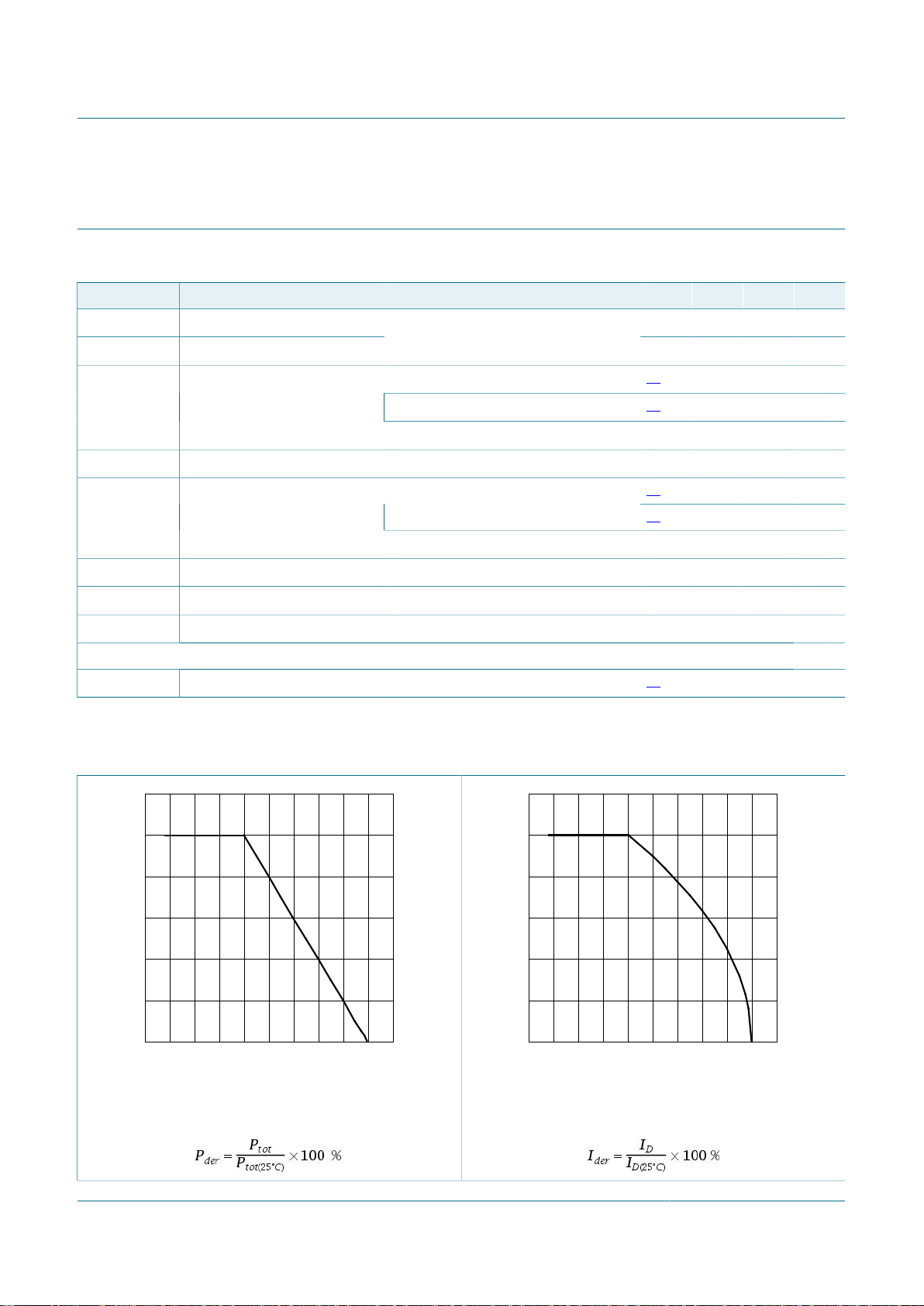
Fig. 1. Normalized total power dissipation as a
function of junction temperature
BSN20BK All information provided in this document is subject to legal disclaimers. © NXP Semiconductors N.V. 2014. All rights reserved
Product data sheet 18 December 2014 3 / 16
Fig. 2. Normalized continuous drain current as a
function of junction temperature

NXP Semiconductors
aaa-015759
VDS (V)
10
-1
10
2
101
10
-1
10
-2
1
I
D
(A)
10
-3
Limit R
DSon
= VDS/I
D
(1)
(2)
(3)
(4)
(5)
(6)
(7)
BSN20BK
60 V, N-channel Trench MOSFET
IDM = single pulse
(1) tp = 10 µs
(2) tp = 100 µs
(3) tp = 1 ms
(4) tp = 10 ms
(5) DC; Tsp = 25 °C
(6) tp = 100 ms
(7) DC; T
= 25 °C; drain mounting pad 1 cm
amb
Fig. 3. Safe operating area; junction to ambient; continuous and peak drain currents as a function of drain-
source voltage
2
9. Thermal characteristics
Table 6. Thermal characteristics
Symbol Parameter Conditions Min Typ Max Unit
R
th(j-a)
thermal resistance
from junction to
ambient
R
th(j-sp)
thermal resistance
from junction to solder
point
[1] Device mounted on an FR4 PCB, single-sided copper, tin-plated and standard footprint.
[2]
BSN20BK All information provided in this document is subject to legal disclaimers. © NXP Semiconductors N.V. 2014. All rights reserved
Product data sheet 18 December 2014 4 / 16
Device mounted on an FR4 PCB, single-sided copper, tin-plated and mounting pad for drain 1 cm2.
in free air [1] - 351 404 K/W
[2] - 271 311 K/W
t ≤ 5 s [2] - 210 241 K/W
- 65 75 K/W

NXP Semiconductors
aaa-014128
tp (s)
10
-3
10
2
10
3
10110
-2
10
-1
10
2
10
3
Z
th(j-a)
(K/W)
10
duty cycle = 1
0.75
0.33
0.25
0.05
0.02
0.01
0
0.10
0.20
0.50
aaa-014129
tp (s)
10
-3
10
2
10
3
10110
-2
10
-1
10
2
10
3
Z
th(j-a)
(K/W)
10
0.02
0.01
0
duty cycle = 1
0.75
0.33
0.05
0.10
0.20
0.50
0.25
BSN20BK
60 V, N-channel Trench MOSFET
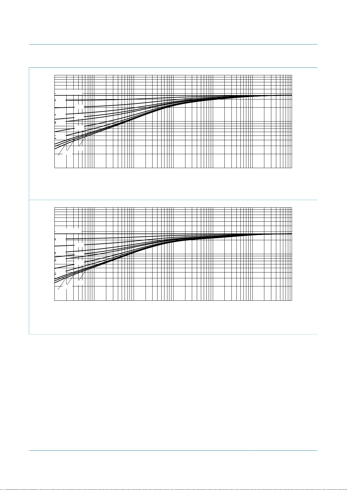
FR4 PCB, standard footprint
Fig. 4. Transient thermal impedance from junction to ambient as a function of pulse duration; typical values
FR4 PCB, mounting pad for drain 1 cm
2
Fig. 5. Transient thermal impedance from junction to ambient as a function of pulse duration; typical values
BSN20BK All information provided in this document is subject to legal disclaimers. © NXP Semiconductors N.V. 2014. All rights reserved
Product data sheet 18 December 2014 5 / 16

NXP Semiconductors
BSN20BK
60 V, N-channel Trench MOSFET
10. Characteristics
Table 7. Characteristics
Symbol Parameter Conditions Min Typ Max Unit
Static characteristics
V
(BR)DSS
V
GSth
I
DSS
I
GSS
drain-source
ID = 250 µA; VGS = 0 V; Tj = 25 °C 60 - - V
breakdown voltage
gate-source threshold
ID = 250 µA; VDS = VGS; Tj = 25 °C 0.6 1 1.4 V
voltage
drain leakage current VDS = 60 V; VGS = 0 V; Tj = 25 °C - - 1 µA
gate leakage current
VGS = 20 V; VDS = 0 V; Tj = 25 °C - - 10 µA
VGS = -20 V; VDS = 0 V; Tj = 25 °C - - -10 µA
VGS = 10 V; VDS = 0 V; Tj = 25 °C - - 1 µA
VGS = -10 V; VDS = 0 V; Tj = 25 °C - - -1 µA
R
DSon
drain-source on-state
resistance
g
fs
forward
transconductance
Dynamic characteristics
Q
Q
Q
C
C
C
G(tot)
GS
GD
iss
oss
rss
total gate charge - 0.49 - nC
gate-source charge - 0.12 - nC
gate-drain charge
input capacitance - 20.2 - pF
output capacitance - 3.1 10 pF
reverse transfer
capacitance
t
d(on)
t
r
t
d(off)
t
f
turn-on delay time - 7.9 - ns
rise time - 8.4 - ns
turn-off delay time - 12.5 - ns
fall time
Source-drain diode
V
SD
source-drain voltage IS = 200 mA; VGS = 0 V; Tj = 25 °C - 0.86 1.2 V
VGS = 5 V; VDS = 0 V; Tj = 25 °C - - 0.3 µA
VGS = -5 V; VDS = 0 V; Tj = 25 °C - - -0.3 µA
VGS = 10 V; ID = 200 mA; Tj = 25 °C - 2.1 2.8 Ω
VGS = 10 V; ID = 200 mA; Tj = 150 °C - 4.3 5.7 Ω
VGS = 5 V; ID = 200 mA; Tj = 25 °C - 2.2 3.2 Ω
VGS = 2.5 V; ID = 75 mA; Tj = 25 °C - 2.6 4 Ω
VDS = 10 V; ID = 200 mA; Tj = 25 °C - 0.71 - S
VDS = 30 V; ID = 200 mA; VGS = 4.5 V;
Tj = 25 °C
- 0.12 - nC
VDS = 30 V; f = 1 MHz; VGS = 0 V;
Tj = 25 °C
- 2 7 pF
VDS = 30 V; ID = 200 mA; VGS = 4.5 V;
R
= 6 Ω; Tj = 25 °C
G(ext)
- 5.1 - ns
BSN20BK All information provided in this document is subject to legal disclaimers. © NXP Semiconductors N.V. 2014. All rights reserved
Product data sheet 18 December 2014 6 / 16
 Loading...