

查询BLF6G10LS-200供应商
BLF6G10LS-200
Power LDMOS transistor
Rev. 01 — 18 January 2008 Preliminary data sheet
1. Product profile
1.1 General description
200 W LDMOS power transistor for base station applications at frequencies from
800 MHz to 1000 MHz.
Table 1. Typical performance
Typical RF performance at T
Mode of operation f V
2-carrier W-CDMA 869 to 894 28 40 20 27 −41
= 25°C in a class-AB production test circuit.
case
P
DS
(MHz) (V) (W) (dB) (%) (dBc)
L(AV)
G
p
η
ACPR
D
[1]
CAUTION
[1] Test signal: 3GPP; test model 1; 64 DPCH; PAR = 7.5 dB at 0.01 % probability on CCDF per carrier; carrier
spacing 5 MHz.
This device is sensitive to ElectroStatic Discharge (ESD). Therefore care should be taken
during transport and handling.
1.2 Features
n Typical 2-carrier W-CDMA performance at frequencies of 869 MHz and 894 MHz, a
supply voltage of 28 V and an IDq of 1400 mA:
u Average output power = 40 W
u Power gain = 20 dB
u Efficiency = 27 %
u ACPR = −41 dBc
n Easy power control
n Integrated ESD protection
n Excellent ruggedness
n High efficiency
n Excellent thermal stability
n Designed for broadband operation (800 MHz to 1000 MHz)
n Internally matched for ease of use
n Compliant to Directive 2002/95/EC, regarding Restriction of Hazardous Substances
(RoHS)
NXP Semiconductors
1.3 Applications
n RF power amplifiers for GSM, GSM EDGE, W-CDMA and CDMA base stations and
multicarrier applications in the 800 MHz to 1000 MHz frequency range.
2. Pinning information
Table 2. Pinning
Pin Description Simplified outline Symbol
1 drain
2 gate
3 source
[1] Connected to flange
3. Ordering information
BLF6G10LS-200
Power LDMOS transistor
2
sym112
1
3
1
[1]
3
2
Table 3. Ordering information
Type number Package
BLF6G10LS-200 - earless flanged LDMOST ceramic package; 2 leads SOT502B
4. Limiting values
Table 4. Limiting values
In accordance with the Absolute Maximum Rating System (IEC 60134).
Symbol Parameter Conditions Min Max Unit
V
DS
V
GS
I
D
T
stg
T
j
drain-source voltage - 65 V
gate-source voltage −0.5 +13 V
drain current - 49 A
storage temperature −65 +150 °C
junction temperature - 225 °C
5. Thermal characteristics
Table 5. Thermal characteristics
Symbol Parameter Conditions Typ Unit
R
th(j-case)
thermal resistance from junction to case T
Name Description Version
=80°C; PL= 40 W 0.34 K/W
case
BLF6G10LS-200_1 © NXP B.V. 2008. All rights reserved.
Preliminary data sheet Rev. 01 — 18 January 2008 2 of 11

NXP Semiconductors
6. Characteristics
Table 6. Characteristics
Tj = 25°C unless otherwise specified.
Symbol Parameter Conditions Min Typ Max Unit
V
(BR)DSS
V
GS(th)
V
GSq
I
DSS
I
DSX
I
GSS
g
fs
R
DS(on)
C
rs
BLF6G10LS-200
Power LDMOS transistor
drain-source breakdown
voltage
gate-source threshold voltage VDS=10V;ID= 270 mA 1.4 1.9 2.4 V
gate-source quiescent voltage VDS= 28 V;
drain leakage current VGS=0V; VDS=28V - - 5 µA
drain cut-off current VGS=V
gate leakage current VGS= 11 V; VDS= 0 V - - 450 nA
forward transconductance VDS=10V; ID= 9.45 A - 19 - S
drain-source on-state
resistance
feedback capacitance VGS=0V; VDS=28V;
VGS=0V; ID= 0.9 mA 65 - - V
1.7 2.2 2.7 V
I
= 1620 mA
D
V
=10V
DS
VGS=V
I
= 9.45 A
D
GS(th)
GS(th)
+ 3.75 V;
+ 3.75 V;
40 45 - A
- 0.06 - Ω
- 3.7 - pF
f= 1MHz
7. Application information
Table 7. Application information
Mode of operation: 2-carrier W-CDMA; PAR 7.5 dB at 0.01 % probability on CCDF; 3GPP test
model 1; 1-64 PDPCH; f
RF performance at V
class-AB production test circuit.
Symbol Parameter Conditions Min Typ Max Unit
P
L(AV)
G
p
RL
in
η
D
ACPR adjacent channel power ratio P
7.1 Ruggedness in class-AB operation
The BLF6G10LS-200 is capable of withstanding a load mismatch corresponding to
VSWR = 7 : 1 through all phases under the following conditions: VDS=28V;
IDq= 1400 mA; PL= 200 W; f = 894 MHz.
average output power - 40 - W
power gain P
input return loss P
drain efficiency P
= 871.5 MHz; f2= 876.5 MHz; f3= 886.5 MHz; f4= 891.5 MHz;
1
=28V; IDq= 1400 mA; T
DS
=25°C; unless otherwise specified; in a
case
= 40 W 18.5 20.2 21.5 dB
L(AV)
= 40 W - −6.4 −4.5 dB
L(AV)
= 40 W 24 27 - %
L(AV)
= 40 W - −41 −37 dBc
L(AV)
BLF6G10LS-200_1 © NXP B.V. 2008. All rights reserved.
Preliminary data sheet Rev. 01 — 18 January 2008 3 of 11
NXP Semiconductors
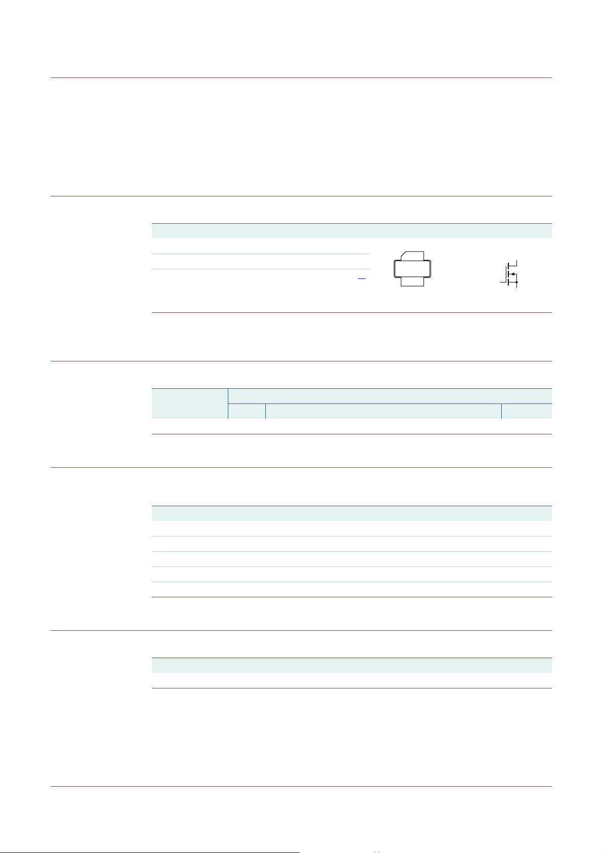
7.2 One-tone CW
BLF6G10LS-200
Power LDMOS transistor
VDS = 28 V; IDq = 1400 mA; f = 894 MHz.
Fig 1. One-tone CW power gain and drain efficiency as functions of load power;
typical values
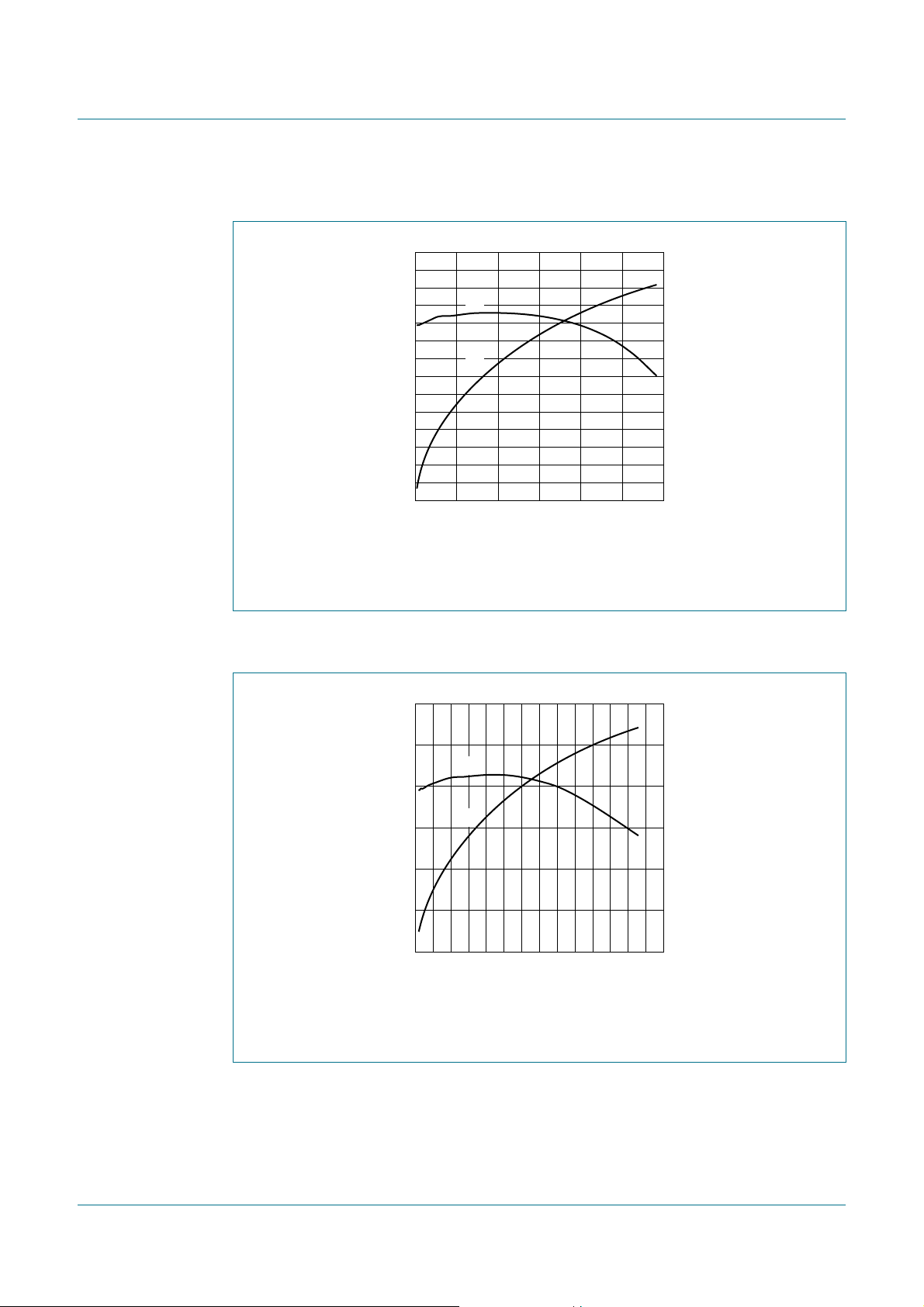
7.3 Two-tone CW
22
G
p
(dB)
21
20
19
18
17
16
15
0 2401608040 120 200
G
p
η
D
001aah526
PL (W)
70
η
D
(%)
60
50
40
30
20
10
0
22
G
p
(dB)
20
18
16
0 350300100 20050 150 250
G
p
η
D
001aah534
P
L(PEP)
(W)
60
η
D
(%)
40
20
0
VDS = 28 V; IDq = 1400 mA; f1 = 893.95 MHz; f2 = 894.05 MHz.
Fig 2. Two-tone CW power gain and drain efficiency as functions of peak envelope load
power; typical values
BLF6G10LS-200_1 © NXP B.V. 2008. All rights reserved.
Preliminary data sheet Rev. 01 — 18 January 2008 4 of 11

NXP Semiconductors
BLF6G10LS-200
Power LDMOS transistor
0
IMD
(dBc)
−20
−40
−60
−80
0 350300100 20050 150 250
001aah535
IMD3
IMD5
IMD7
P
L(PEP)
(W)
VDS = 28 V; IDq = 1400 mA; f1 = 893.95 MHz;
f2= 894.05 MHz.
Fig 3. Two-tone CW intermodulation distortion as
function of peak envelope load power; typical
values
0
IMD3
(dBc)
−20
−40
−60
−80
0 350300100 20050 150 250
(5)
(4)
(1)
(3)
(2)
001aah536
P
L(PEP)
(W)
VDS = 28 V; f1 = 893.95 MHz; f2= 894.05 MHz.
(1) 1300 MHz
(2) 1350 MHz
(3) 1400 MHz
(4) 1450 MHz
(5) 1500 MHz
Fig 4. Third order intermodulation distortion as a
function of peak envelope load power; typical
values
7.4 2-carrier W-CDMA
P
L(AV)
001aah537
(W)
22
G
p
(dB)
21
G
20
19
18
17
0604020
p
η
D
VDS = 28 V; IDq = 1400 mA; f1 = 886.5 MHz;
f2= 891.5 MHz; carrier spacing 5 MHz.
Fig 5. 2-carrier W-CDMA power gain and drain
efficiency as functions of average load power;
typical values
50
η
D
(%)
40
30
20
10
0
0
ACPR
(dBc)
−20
−40
−60
−80
0706020 4010 30 50
001aah538
P
(W)
L(AV)
VDS = 28 V; IDq = 1400 mA; f1 = 886.5 MHz;
f2= 891.5 MHz; carrier spacing 5 MHz.
Fig 6. 2-carrierW-CDMA adjacent channel power ratio
as function of average load power; typical
values
BLF6G10LS-200_1 © NXP B.V. 2008. All rights reserved.
Preliminary data sheet Rev. 01 — 18 January 2008 5 of 11

NXP Semiconductors
8. Test information
BLF6G10LS-200
Power LDMOS transistor
V
GG
R3
input
50 Ω
C2 C5
C14 C20
The striplines are on a double copper-clad Taconic RF35 Printed-Circuit Board (PCB) with εr= 3.5 and
thickness = 0.76 mm.
See Table 8 for list of components.
Fig 7. Test circuit for operation at 800 MHz
R2
C1
R2
C15
C6 C7 C3 C10C1
C8 C9 C4 C11 C12
C6
C7
C3
Q3
C10
V
R1
L1
C13
DD
C13
output
50 Ω
001aah539
R3
L1
R1
C15C14C2
NXP
IN
800 -1000 MHz
V1.0
C18
C19
C9C8
NXP
OUT
800 -1000 MHz
V1.0
C5
C20
C4
C11
C12
001aah540
The striplines are on a double copper-clad Taconic RF35 Printed-Circuit Board (PCB) with εr= 3.5 and
thickness = 0.76 mm.
See Table 8 for list of components.
Fig 8. Component layout
BLF6G10LS-200_1 © NXP B.V. 2008. All rights reserved.
Preliminary data sheet Rev. 01 — 18 January 2008 6 of 11
NXP Semiconductors
BLF6G10LS-200
Power LDMOS transistor
Table 8. List of components (see Figure 7 and Figure 8)
All capacitors should be soldered vertically except C20.
Component Description Value Remarks
C1, C2, C3, C4, C5 multilayer ceramic chip capacitor 68 pF
C6, C7, C8, C9 multilayer ceramic chip capacitor 330 nF
C10, C11 multilayer ceramic chip capacitor 4.7 µF
C12, C13 Electrolytic capacitor 220 µF; 63 V
C14 multilayer ceramic chip capacitor 4.7 pF; 50 V
C15 multilayer ceramic chip capacitor 9.1 pF
C18, C19 multilayer ceramic chip capacitor 10 pF
C20 multilayer ceramic chip capacitor 1.5 pF; 20 V
L1 Ferrite SMD bead - Ferroxcube BDS 3/3/4.6-4S2 or equivalent
Q1 BLC6G10LS-160 R1, R2, R3 SMD resistor 9.1 Ω; 0.1 W
[1] American Technical Ceramics type 100B or capacitor of same quality.
[2] TDK or capacitor of same quality.
[1]
[2]
[2]
[1]
[1]
[1]
[1]
BLF6G10LS-200_1 © NXP B.V. 2008. All rights reserved.
Preliminary data sheet Rev. 01 — 18 January 2008 7 of 11

NXP Semiconductors
BLF6G10LS-200
Power LDMOS transistor
9. Package outline
Earless flanged LDMOST ceramic package; 2 leads SOT502B
D
A
F
3
D
1
U
1
L
H
U
2
1
D
c
E
1
E
2
b
w
M M
D
2
0 5 10 mm
scale
Q
DIMENSIONS (millimetre dimensions are derived from the original inch dimensions)
UNIT
mm
inches
A
4.72
3.43
0.186
0.135
OUTLINE
VERSION
SOT502B
12.83
12.57
0.505
0.495
c
Db
20.02
19.61
0.788
0.772
19.96
19.66
0.786
0.774
0.15
0.08
0.006
0.003
IEC JEDEC JEITA
D
1
EE
9.53
9.50
9.25
9.30
0.374
0.375
0.366
0.364
REFERENCES
1
0.045
0.035
F
1.14
0.89
H
19.94
18.92
0.785
0.745
L
5.33
4.32
0.210
0.170
Q
1.70
1.45
0.067
0.057
U
1
20.70
20.45
0.815
0.805
U
9.91
9.65
0.390
0.380
2
w
2
0.25
0.010
EUROPEAN
PROJECTION
ISSUE DATE
03-01-10
07-05-09
Fig 9. Package outline SOT502B
BLF6G10LS-200_1 © NXP B.V. 2008. All rights reserved.
Preliminary data sheet Rev. 01 — 18 January 2008 8 of 11

NXP Semiconductors
10. Abbreviations
Table 9. Abbreviations
Acronym Description
3GPP Third Generation Partnership Project
CCDF Complementary Cumulative Distribution Function
CDMA Code Division Multiple Access
CW Continuous Wave
DPCH Dedicated Physical CHannel
EDGE Enhanced Data rates for GSM Evolution
GSM Global System for Mobile communications
LDMOS Laterally Diffused Metal Oxide Semiconductor
LDMOST Laterally Diffused Metal-Oxide Semiconductor Transistor
PAR Peak-to-Average power Ratio
PDPCH transmission Power of the Dedicated Physical CHannel
RF Radio Frequency
VSWR Voltage Standing Wave Ratio
W-CDMA Wideband Code Division Multiple Access
BLF6G10LS-200
Power LDMOS transistor
11. Revision history
Table 10. Revision history
Document ID Release date Data sheet status Change notice Supersedes
BLF6G10LS-200_1 20080118 Preliminary data sheet - -
BLF6G10LS-200_1 © NXP B.V. 2008. All rights reserved.
Preliminary data sheet Rev. 01 — 18 January 2008 9 of 11

NXP Semiconductors
12. Legal information
12.1 Data sheet status
BLF6G10LS-200
Power LDMOS transistor
Document status
Objective [short] data sheet Development This document contains data from the objective specification for product development.
Preliminary [short] data sheet Qualification This document contains data from the preliminary specification.
Product [short] data sheet Production This document contains the product specification.
[1] Please consult the most recently issued document before initiating or completing a design.
[2] The term ‘short data sheet’ is explained in section “Definitions”.
[3] The product status of device(s)described in this document mayhave changed since thisdocument was published and maydiffer incase of multiple devices.The latest productstatus
information is available on the Internet at URL
[1][2]
Product status
12.2 Definitions
Draft — The document is a draft version only. The content is still under
internal review and subject to formal approval, which may result in
modifications or additions. NXP Semiconductors does not give any
representations or warranties as to the accuracy or completeness of
information includedherein and shallhave noliability for theconsequences of
use of such information.
Short data sheet — A short data sheet is an extract from a full data sheet
with thesame product typenumber(s)and title.Ashort data sheet isintended
for quickreference only and shouldnot be relied upon tocontaindetailed and
full information. For detailed and full information see the relevant full data
sheet, which is available on request via the local NXP Semiconductors sales
office. In case of any inconsistency or conflict with the short data sheet, the
full data sheet shall prevail.
12.3 Disclaimers
General — Information in this document is believed to be accurate and
reliable. However,NXP Semiconductors does not giveany representations or
warranties, expressed or implied, asto the accuracy orcompleteness of such
information and shall have no liability for the consequences of use of such
information.
Right to make changes — NXP Semiconductors reserves the right tomake
changes to information published in this document, including without
limitation specifications and product descriptions, at any time and without
notice. Thisdocumentsupersedes and replaces all informationsupplied prior
to the publication hereof.
Suitability for use — NXP Semiconductors products are not designed,
authorized or warranted to be suitable for use in medical, military, aircraft,
space or life support equipment, nor in applications where failure or
[3]
http://www.nxp.com.
Definition
malfunction of an NXP Semiconductors product can reasonably be expected
to result in personal injury, death or severe property or environmental
damage. NXP Semiconductors accepts no liability for inclusion and/or use of
NXP Semiconductors products in such equipment or applications and
therefore such inclusion and/or use is at the customer’s own risk.
Applications — Applications that are described herein for any of these
products are for illustrative purposes only. NXP Semiconductors makes no
representation or warranty that such applications will be suitable for the
specified use without further testing or modification.
Limiting values — Stress above one or more limiting values (as defined in
the Absolute MaximumRatings System of IEC 60134)may cause permanent
damage tothe device. Limiting values are stressratings only and operationof
the device at these or any other conditions above those given in the
Characteristics sections of this document is not implied. Exposure to limiting
values for extended periods may affect device reliability.
Terms and conditions of sale — NXP Semiconductors products are sold
subject to the general terms and conditions ofcommercial sale, as published
at
http://www.nxp.com/profile/terms, including those pertaining to warranty,
intellectual property rights infringement and limitation of liability, unless
explicitly otherwise agreed to in writing by NXP Semiconductors. In case of
any inconsistency or conflict between information in this document and such
terms and conditions, the latter will prevail.
No offer to sell or license — Nothing in this document may be interpreted
or construed as an offer to sell products that is open for acceptance or the
grant, conveyance or implication ofany license under any copyrights,patents
or other industrial or intellectual property rights.
12.4 Trademarks
Notice: Allreferenced brands,product names, servicenamesand trademarks
are the property of their respective owners.
13. Contact information
For additional information, please visit: http://www.nxp.com
For sales office addresses, send an email to: salesaddresses@nxp.com
BLF6G10LS-200_1 © NXP B.V. 2008. All rights reserved.
Preliminary data sheet Rev. 01 — 18 January 2008 10 of 11

NXP Semiconductors
14. Contents
1 Product profile . . . . . . . . . . . . . . . . . . . . . . . . . . 1
1.1 General description. . . . . . . . . . . . . . . . . . . . . . 1
1.2 Features . . . . . . . . . . . . . . . . . . . . . . . . . . . . . . 1
1.3 Applications . . . . . . . . . . . . . . . . . . . . . . . . . . . 2
2 Pinning information. . . . . . . . . . . . . . . . . . . . . . 2
3 Ordering information. . . . . . . . . . . . . . . . . . . . . 2
4 Limiting values. . . . . . . . . . . . . . . . . . . . . . . . . . 2
5 Thermal characteristics. . . . . . . . . . . . . . . . . . . 2
6 Characteristics. . . . . . . . . . . . . . . . . . . . . . . . . . 3
7 Application information. . . . . . . . . . . . . . . . . . . 3
7.1 Ruggedness in class-AB operation. . . . . . . . . . 3
7.2 One-tone CW . . . . . . . . . . . . . . . . . . . . . . . . . . 4
7.3 Two-tone CW . . . . . . . . . . . . . . . . . . . . . . . . . . 4
7.4 2-carrier W-CDMA . . . . . . . . . . . . . . . . . . . . . . 5
8 Test information. . . . . . . . . . . . . . . . . . . . . . . . . 6
9 Package outline . . . . . . . . . . . . . . . . . . . . . . . . . 8
10 Abbreviations. . . . . . . . . . . . . . . . . . . . . . . . . . . 9
11 Revision history. . . . . . . . . . . . . . . . . . . . . . . . . 9
12 Legal information. . . . . . . . . . . . . . . . . . . . . . . 10
12.1 Data sheet status . . . . . . . . . . . . . . . . . . . . . . 10
12.2 Definitions. . . . . . . . . . . . . . . . . . . . . . . . . . . . 10
12.3 Disclaimers . . . . . . . . . . . . . . . . . . . . . . . . . . . 10
12.4 Trademarks. . . . . . . . . . . . . . . . . . . . . . . . . . . 10
13 Contact information. . . . . . . . . . . . . . . . . . . . . 10
14 Contents . . . . . . . . . . . . . . . . . . . . . . . . . . . . . . 11
BLF6G10LS-200
Power LDMOS transistor
Please be aware that important notices concerning this document and the product(s)
described herein, have been included in section ‘Legal information’.
© NXP B.V. 2008. All rights reserved.
For more information, please visit: http://www.nxp.com
For sales office addresses, please send an email to: salesaddresses@nxp.com
Date of release: 18 January 2008
Document identifier: BLF6G10LS-200_1
 Loading...