

DISCRETE SEMICONDUCTORS
BFG410W
NPN 22 GHz wideband transistor
Product specification
Supersedes data of 1997 Oct 29
File under Discrete Semiconductors, SC14
1998 Mar 11
Philips Semiconductors Product specification
NPN 22 GHz wideband transistor BFG410W
FEATURES
• Very high power gain
• Low noise figure
• High transition frequency
• Emitter is thermal lead
• Low feedback capacitance.
APPLICATIONS
• RF front end
• Wideband applications, e.g. analog and digital cellular
telephones, cordless telephones (PHS, DECT, etc.)
• Radar detectors
• Pagers
• Satellite television tuners (SATV)
• High frequency oscillators.
DESCRIPTION
NPN double polysilicon wideband transistor with buried
layer for low voltage applications in a plastic, 4-pin
dual-emitter SOT343R package.
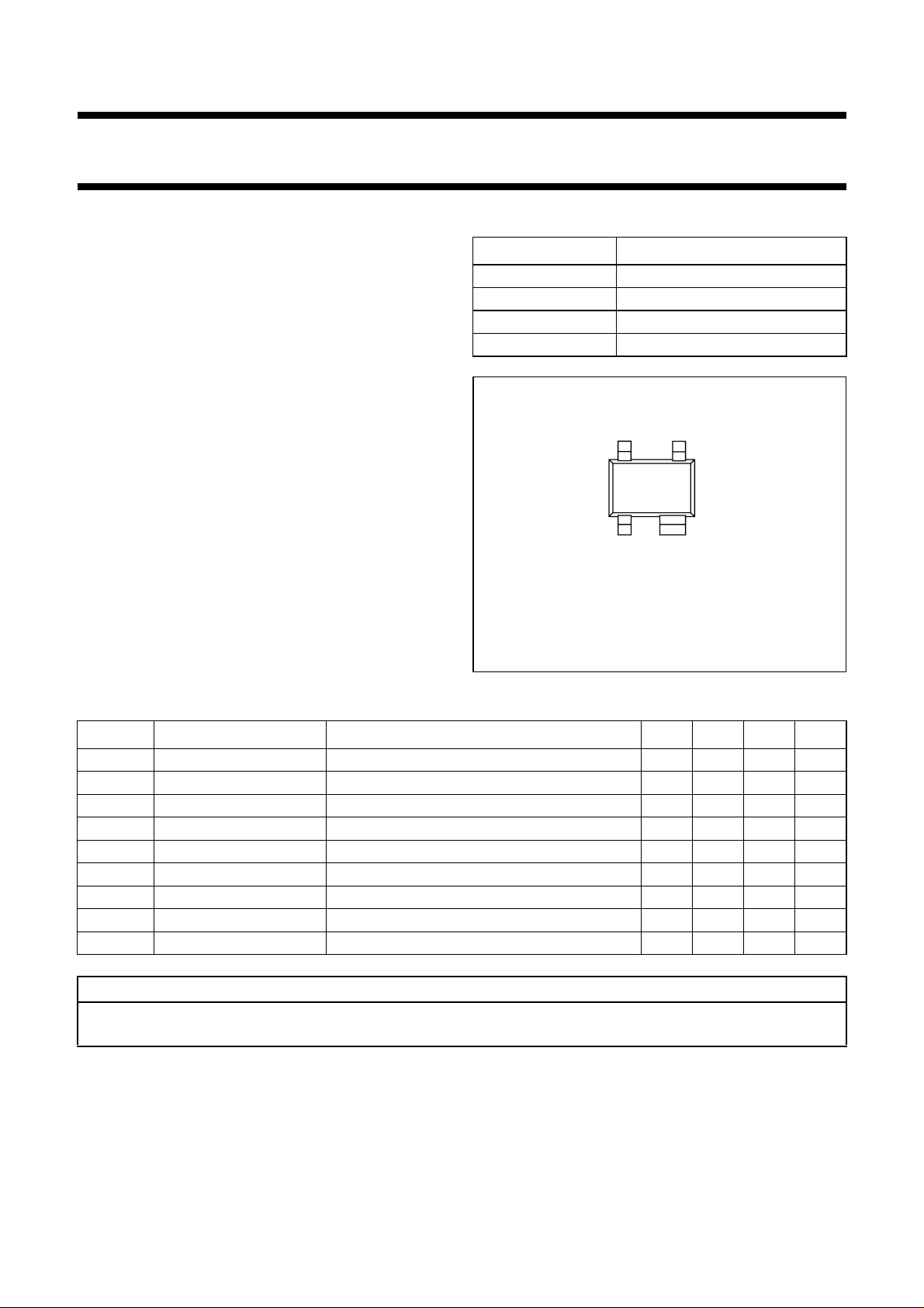
PINNING
PIN DESCRIPTION
handbook, halfpage
Marking code: P4.
1 emitter
2 base
3 emitter
4 collector
43
21
Top view
MSB842
Fig.1 Simplified outline SOT343R.
QUICK REFERENCE DATA
SYMBOL PARAMETER CONDITIONS MIN. TYP. MAX. UNIT
V
CBO
V
CEO
I
C
P
tot
h
FE
C
re
f
T
G
max
F noise figure I
collector-base voltage open emitter −−10 V
collector-emitter voltage open base −−4.5 V
collector current (DC) − 10 12 mA
total power dissipation Ts≤ 110 °C −−54 mW
DC current gain IC= 10 mA; VCE=2V; Tj=25°C 5080120
feedback capacitance IC= 0; VCB= 2 V; f = 1 MHz − 45 − fF
transition frequency IC= 10 mA; VCE= 2 V; f = 2 GHz; T
maximum power gain IC= 10 mA; VCE= 2 V; f = 2 GHz; T
= 1 mA; VCE= 2 V; f = 2 GHz; ΓS= Γ
C
=25°C − 22 − GHz
amb
=25°C − 21 − dB
amb
opt
− 1.2 − dB
CAUTION
This product is supplied in anti-static packing to prevent damage caused by electrostatic discharge during transport
and handling. For further information, refer to Philips specs.: SNW-EQ-608, SNW-FQ-302A and SNW-FQ-302B.
1998 Mar 11 2

Philips Semiconductors Product specification
NPN 22 GHz wideband transistor BFG410W
LIMITING VALUES
In accordance with the Absolute Maximum Rating System (IEC 134).
SYMBOL PARAMETER CONDITIONS MIN. MAX. UNIT
V
CBO
V
CEO
V
EBO
I
C
P
tot
T
stg
T
j
Note
1. T
s
THERMAL CHARACTERISTICS
collector-base voltage open emitter − 10 V
collector-emitter voltage open base − 4.5 V
emitter-base voltage open collector − 1V
collector current (DC) − 12 mA
total power dissipation Ts≤ 110 °C; note 1; see Fig.2 − 54 mW
storage temperature −65 +150 °C
operating junction temperature − 150 °C
is the temperature at the soldering point of the emitter pins.
SYMBOL PARAMETER VALUE UNIT
R
th j-s
handbook, halfpage
(mW)
thermal resistance from junction to soldering point 750 K/W
120
MGD960
Ts (°C)
60
P
tot
40
20
0
0
40 80 160
Fig.2 Power derating curve.
1998 Mar 11 3

Philips Semiconductors Product specification
NPN 22 GHz wideband transistor BFG410W
CHARACTERISTICS
T
=25°C unless otherwise specified.
j
SYMBOL PARAMETER CONDITIONS MIN. TYP. MAX. UNIT
V
(BR)CBO
V
(BR)CEO
V
(BR)EBO
I
CBO
h
FE
C
c
C
e
C
re
f
T
G
max
S
21
F noise figure I
P
L1
ITO third order intercept point I
collector-base breakdown voltage IC= 2.5 µA; IE=0 10 −−V
collector-emitter breakdown
IC= 1 mA; IB= 0 4.5 −−V
voltage
emitter-base breakdown voltage IE= 2.5 µA; IC=0 1 −−V
collector-base leakage current IE= 0; VCB= 4.5 V −−15 nA
DC current gain IC= 10 mA; VCE= 2 V; see Fig.3 50 80 120
collector capacitance IE=ie= 0; VCB=2V; f=1MHz − 220 − fF
emitter capacitance IC=ic= 0; VEB= 0.5 V; f = 1 MHz − 400 − fF
feedback capacitance IC= 0; VCB= 2 V; f = 1 MHz;
− 45 − fF
see Fig.4
transition frequency IC= 10 mA; VCE= 2 V; f = 2 GHz;
T
=25°C; see Fig.5
amb
maximum power gain; note 1 IC= 10 mA; VCE= 2 V; f = 2 GHz;
T
=25°C; see Figs 7 and 8
amb
insertion power gain I
2
= 10 mA; VCE= 2 V; f = 2 GHz;
C
T
=25°C; see Fig.8
amb
= 1 mA; VCE=2V;
C
f = 900 MHz; ΓS= Γ
I
= 1 mA; VCE= 2 V; f = 2 GHz;
C
output power at 1 dB gain
compression
ΓS= Γ
IC= 10 mA; VCE= 2 V; f = 2 GHz;
ZS=Z
C
ZS=Z
; see Fig.13
opt
; ZL=Z
S opt
= 10 mA; VCE= 2 V; f = 2 GHz;
; ZL=Z
S opt
; see Fig.13
opt
; note 2
L opt
; note 2
L opt
− 22 − GHz
− 21 − dB
− 18 − dB
− 0.9 − dB
− 1.2 − dB
− 5 − dBm
− 15 − dBm
Notes
1. G
is the maximum power gain, if K > 1. If K < 1 then G
max
2. ZS is optimized for noise; ZL is optimized for gain.
1998 Mar 11 4
= MSG; see Figs 6, 7 and 8.
max

Philips Semiconductors Product specification
NPN 22 GHz wideband transistor BFG410W
120
handbook, halfpage
h
FE
100
80
60
40
20
0
0 4 12 168
(1) VCE=3V.
(2) VCE=2V.
(3) VCE=1V.
MGG717
(1)
(2)
(3)
IC (mA)
Fig.3 DC current gain as a function of collector
current; typical values.
100
handbook, halfpage
C
re
(fF)
80
60
40
20
0
01 5
IC= 0; f= 1 MHz.
23 4
VCB (V)
Fig.4 Feedback capacitance as a function of
collector-base voltage; typical values.
MGG718
25
handbook, halfpage
f
T
(GHz)
20
15
10
5
0
11010
VCE= 2 V; f = 2 GHz; T
amb
IC (mA)
=25°C.
MGG719
2
Fig.5 Transition frequency as a function of
collector current; typical values.
1998 Mar 11 5
30
handbook, halfpage
MSG
(dB)
20
10
0
048 1612
VCE= 2 V; f = 900 MHz.
IC (mA)
Fig.6 Maximum stable gain as a function of
collector current; typical values.
MGG720

Philips Semiconductors Product specification
NPN 22 GHz wideband transistor BFG410W
30
handbook, halfpage
gain
(dB)
20
10
0
0812416
VCE= 2 V; f = 2 GHz.
MSG
G
IC (mA)
Fig.7 Gain as a function of collector current;
typical values.
MGG721
max
50
handbook, halfpage
gain
(dB)
40
30
20
10
0
10 10
IC= 10 mA; VCE=2V.
S
2
MSG
21
10
Fig.8 Gain as a function of frequency;
typical values.
3
f (MHz)
MGG722
4
10
handbook, full pagewidth
IC= 10 mA; VCE= 2 V; Zo=50Ω.
90°
1.0
0.8
0.6
0.4
0.2
0°
0
1.0
180°
1
135°
0
−135°
0.5
0.2
0.2 0.5 1 2 5
3 GHz
0.2
0.5
1
−90°
2
40 MHz
2
45°
5
5
−45°
MGG724
Fig.9 Common emitter input reflection coefficient (S11); typical values.
1998 Mar 11 6

Philips Semiconductors Product specification
NPN 22 GHz wideband transistor BFG410W
handbook, full pagewidth
IC= 10 mA; VCE=2V.
90°
135°
180°
50 40 30 20 10
40 MHz
−135°
3 GHz
−90°
45°
0°
−45°
MGG725
Fig.10 Common emitter forward transmission coefficient (S21); typical values.
handbook, full pagewidth
IC= 10 mA; VCE=2V.
90°
135°
0.1 0.08 0.06 0.04 0.02
180°
−135°
3 GHz
40 MHz
−90°
45°
0°
−45°
MGG726
Fig.11 Common emitter reverse transmission coefficient (S12); typical values.
1998 Mar 11 7

Philips Semiconductors Product specification
NPN 22 GHz wideband transistor BFG410W
handbook, full pagewidth
IC= 10 mA; VCE= 2 V; Zo=50Ω.
90°
1.0
0.8
0.6
0.4
0.2
0°
0
1.0
180°
1
135°
0
−135°
0.5
0.2
0.2 0.5 1 2 5
0.2
0.5
1
−90°
3 GHz
45°
2
5
40 MHz
5
2
−45°
MGG727
Fig.12 Common emitter output reflection coefficient (S22); typical values.
Noise data
V
= 2 V; typical values.
CE
f
(MHz)
I
C
(mA)
F
min
(dB)
Γ
mag
Γ
angle
900 1 0.8 0.73 11.2 0.56
2 0.9 0.58 10.1 0.43
4 1.1 0.40 10.1 0.33
6 1.3 0.28 11.0 0.30
8 1.5 0.20 8.0 0.30
10 1.7 0.14 10.5 0.27
12 1.9 0.06 10.1 0.25
14 2.1 0.05 14.2 0.26
2000 1 1.2 0.64 35.7 0.57
2 1.2 0.50 35.8 0.44
4 1.4 0.34 34.4 0.37
6 1.6 0.25 33.7 0.34
8 1.8 0.17 34.5 0.35
10 2.0 0.12 35.8 0.34
12 2.2 0.05 38.0 0.35
14 2.4 0.03 44.8 0.34
r
(Ω)
n
handbook, halfpage
3
F
min
(dB)
2
1
0
0841216
(1) f = 2 GHz; VCE=2V.
(2) f = 900 MHz; VCE=2V.
(1)
(2)
MGG723
IC (mA)
Fig.13 Minimum noise figure as a function of the
collector current; typical values.
1998 Mar 11 8

Philips Semiconductors Product specification
NPN 22 GHz wideband transistor BFG410W
SPICE parameters for the BFG410W die
SEQUENCE No. PARAMETER VALUE UNIT
1 IS 19.42 aA
2 BF 145.0 −
3 NF 0.993 −
4 VAF 31.12 V
5 IKF 125.0 mA
6 ISE 123.6 fA
7 NE 3.000 −
8 BR 11.37 −
9 NR 0.985 −
10 VAR 1.874 V
11 IKR 50.00 mA
12 ISC 199.6 aA
13 NC 1.546 −
14 RB 35.00 Ω
15 IRB 0.000 A
16 RBM 15.00 Ω
17 RE 432.0 mΩ
18 RC 4.324 Ω
(1)
19
20
21
(1)
(1)
XTB 1.500 −
EG 1.110 eV
XTI 3.000 −
22 CJE 128.0 fF
23 VJE 900.0 mV
24 MJE 0.346 −
25 TF 4.122 ps
26 XTF 68.20 −
27 VTF 2.004 V
28 ITF 0.627 A
29 PTF 0.000 deg
30 CJC 56.68 fF
31 VJC 556.9 mV
32 MJC 0.207 −
33 XCJC 0.500 −
(1)
34
35
36
37
(1)
(1)
(1)
TR 0.000 ns
CJS 274.8 fF
VJS 418.3 mV
MJS 0.239 −
38 FC 0.550 −
SEQUENCE No. PARAMETER VALUE UNIT
(2)(3)
39
40
41
(2)
(3)
C
bp
R
sb1
R
sb2
145 fF
25 Ω
19 Ω
Notes
1. These parameters have not been extracted, the
default values are shown.
2. Bonding pad capacity Cbp in series with substrate
resistance R
between B′ and E′.
sb1
3. Bonding pad capacity Cbp in series with substrate
resistance R
handbook, halfpage
L1 L2
B
C
be ce
QLB= 50; QLE= 50; QL
= scaling frequency = 1 GHz.
f
c
between C′ and E′.
sb2
C
cb
E'
L3
E
(f)=QL
B,E
B,E
√(f/fc)
CB' C'
C
MGD956
Fig.14 Package equivalent circuit SOT343R2.
List of components (see Fig.14)
DESIGNATION VALUE UNIT
C
be
C
cb
C
ce
80 fF
2fF
80 fF
L1 1.1 nH
L2 1.1 nH
L3 (note 1) 0.25 nH
Note
1. External emitter inductance to be added separately
due to the influence of the printed-circuit board.
1998 Mar 11 9

Philips Semiconductors Product specification
NPN 22 GHz wideband transistor BFG410W
PACKAGE OUTLINE
Plastic surface mounted package; reverse pinning; 4 leads SOT343R
w M
D
y
e
43
21
b
B
p
e
b
1
1
E
H
E
A
A
1
detail X
AB
Q
L
p
X
v M
A
c
0 1 2 mm
scale
DIMENSIONS (mm are the original dimensions)
A
1
mm
OUTLINE
VERSION
SOT343R
1.1
0.8
A
max
0.1
b
p
0.4
0.3
IEC JEDEC EIAJ
b
1
0.7
0.5
cD
0.25
2.2
0.10
1.8
E
1.35
1.3
1.15
REFERENCES
e
UNIT
1998 Mar 11 10
H
L
e
E
1
2.2
0.45
2.0
0.15
Qwv
p
0.23
0.13
0.2y0.10.21.15
EUROPEAN
PROJECTION
ISSUE DATE
97-05-21

Philips Semiconductors Product specification
NPN 22 GHz wideband transistor BFG410W
DEFINITIONS
Data Sheet Status
Objective specification This data sheet contains target or goal specifications for product development.
Preliminary specification This data sheet contains preliminary data; supplementary data may be published later.
Product specification This data sheet contains final product specifications.
Limiting values
Limiting values given are in accordance with the Absolute Maximum Rating System (IEC 134). Stress above one or
more of the limiting values may cause permanent damage to the device. These are stress ratings only and operation
of the device at these or at any other conditions above those given in the Characteristics sections of the specification
is not implied. Exposure to limiting values for extended periods may affect device reliability.
Application information
Where application information is given, it is advisory and does not form part of the specification.
LIFE SUPPORT APPLICATIONS
These products are not designed for use in life support appliances, devices, or systems where malfunction of these
products can reasonably be expected to result in personal injury. Philips customers using or selling these products for
use in such applications do so at their own risk and agree to fully indemnify Philips for any damages resulting from such
improper use or sale.
1998 Mar 11 11

Philips Semiconductors – a worldwide company
Argentina: see South America
Australia: 34 Waterloo Road, NORTH RYDE, NSW 2113,
Tel. +61 2 9805 4455, Fax. +61 2 9805 4466
Austria: Computerstr. 6, A-1101 WIEN, P.O. Box 213, Tel. +43 160 1010,
Fax. +43 160 101 1210
Belarus: Hotel Minsk Business Center, Bld. 3, r. 1211, Volodarski Str. 6,
220050 MINSK, Tel. +375 172 200 733, Fax. +375 172 200 773
Belgium: see The Netherlands
Brazil: see South America
Bulgaria: Philips Bulgaria Ltd., Energoproject, 15th floor,
51 James Bourchier Blvd., 1407 SOFIA,
Tel. +359 2 689 211, Fax. +359 2 689 102
Canada: PHILIPS SEMICONDUCTORS/COMPONENTS,
Tel. +1 800 234 7381
China/Hong Kong: 501 Hong Kong Industrial Technology Centre,
72 Tat Chee Avenue, Kowloon Tong, HONG KONG,
Tel. +852 2319 7888, Fax. +852 2319 7700
Colombia: see South America
Czech Republic: see Austria
Denmark: Prags Boulevard 80, PB 1919, DK-2300 COPENHAGEN S,
Tel. +45 32 88 2636, Fax. +45 31 57 0044
Finland: Sinikalliontie 3, FIN-02630 ESPOO,
Tel. +358 9 615800, Fax. +358 9 61580920
France: 51 Rue Carnot, BP317, 92156 SURESNES Cedex,
Tel. +33 1 40 99 6161, Fax. +33 1 40 99 6427
Germany: Hammerbrookstraße 69, D-20097 HAMBURG,
Tel. +49 40 23 53 60, Fax. +49 40 23 536 300
Greece: No. 15, 25th March Street, GR 17778 TAVROS/ATHENS,
Tel. +30 1 4894 339/239, Fax. +30 1 4814 240
Hungary: see Austria
India: Philips INDIA Ltd, Band Box Building, 2nd floor,
254-D, Dr. Annie Besant Road, Worli, MUMBAI 400 025,
Tel. +91 22 493 8541, Fax. +91 22 493 0966
Indonesia: see Singapore
Ireland: Newstead, Clonskeagh, DUBLIN 14,
Tel. +353 1 7640 000, Fax. +353 1 7640 200
Israel: RAPAC Electronics, 7 Kehilat Saloniki St, PO Box 18053,
TEL AVIV 61180, Tel. +972 3 645 0444, Fax. +972 3 649 1007
Italy: PHILIPS SEMICONDUCTORS, Piazza IV Novembre 3,
20124 MILANO, Tel. +39 2 6752 2531, Fax. +39 2 6752 2557
Japan: Philips Bldg 13-37, Kohnan 2-chome, Minato-ku, TOKYO 108,
Tel. +81 3 3740 5130, Fax. +81 3 3740 5077
Korea: Philips House, 260-199 Itaewon-dong, Yongsan-ku, SEOUL,
Tel. +82 2 709 1412, Fax. +82 2 709 1415
Malaysia: No. 76 Jalan Universiti, 46200 PETALING JAYA, SELANGOR,
Tel. +60 3 750 5214, Fax. +60 3 757 4880
Mexico: 5900 Gateway East, Suite 200, EL PASO, TEXAS 79905,
Tel. +9-5 800 234 7381
Middle East: see Italy
Netherlands: Postbus 90050, 5600 PB EINDHOVEN, Bldg. VB,
Tel. +31 40 27 82785, Fax. +31 40 27 88399
New Zealand: 2 Wagener Place, C.P.O. Box 1041, AUCKLAND,
Tel. +64 9 849 4160, Fax. +64 9 849 7811
Norway: Box 1, Manglerud 0612, OSLO,
Tel. +47 22 74 8000, Fax. +47 22 74 8341
Philippines: Philips Semiconductors Philippines Inc.,
106 Valero St. Salcedo Village, P.O. Box 2108 MCC, MAKATI,
Metro MANILA, Tel. +63 2 816 6380, Fax. +63 2 817 3474
Poland: Ul. Lukiska 10, PL 04-123 WARSZAWA,
Tel. +48 22 612 2831, Fax. +48 22 612 2327
Portugal: see Spain
Romania: see Italy
Russia: Philips Russia, Ul. Usatcheva 35A, 119048 MOSCOW,
Tel. +7 095 755 6918, Fax. +7 095 755 6919
Singapore: Lorong 1, Toa Payoh, SINGAPORE 1231,
Tel. +65 350 2538, Fax. +65 251 6500
Slovakia: see Austria
Slovenia: see Italy
South Africa: S.A. PHILIPS Pty Ltd., 195-215 Main Road Martindale,
2092 JOHANNESBURG, P.O. Box 7430 Johannesburg 2000,
Tel. +27 11 470 5911, Fax. +27 11 470 5494
South America: Al. Vicente Pinzon, 173, 6th floor,
04547-130 SÃO PAULO, SP, Brazil,
Tel. +55 11 821 2333, Fax. +55 11 821 2382
Spain: Balmes 22, 08007 BARCELONA,
Tel. +34 3 301 6312, Fax. +34 3 301 4107
Sweden: Kottbygatan 7, Akalla, S-16485 STOCKHOLM,
Tel. +46 8 632 2000, Fax. +46 8 632 2745
Switzerland: Allmendstrasse 140, CH-8027 ZÜRICH,
Tel. +41 1 488 2686, Fax. +41 1 488 3263
Taiwan: Philips Semiconductors, 6F, No. 96, Chien Kuo N. Rd., Sec. 1,
TAIPEI, Taiwan Tel. +886 2 2134 2865, Fax. +886 2 2134 2874
Thailand: PHILIPS ELECTRONICS (THAILAND) Ltd.,
209/2 Sanpavuth-Bangna Road Prakanong, BANGKOK 10260,
Tel. +66 2 745 4090, Fax. +66 2 398 0793
Turkey: Talatpasa Cad. No. 5, 80640 GÜLTEPE/ISTANBUL,
Tel. +90 212 279 2770, Fax. +90 212 282 6707
Ukraine: PHILIPS UKRAINE, 4 Patrice Lumumba str., Building B, Floor 7,
252042 KIEV, Tel. +380 44 264 2776, Fax. +380 44 268 0461
United Kingdom: Philips Semiconductors Ltd., 276 Bath Road, Hayes,
MIDDLESEX UB3 5BX, Tel. +44 181 730 5000, Fax. +44 181 754 8421
United States: 811 East Arques Avenue, SUNNYVALE, CA 94088-3409,
Tel. +1 800 234 7381
Uruguay: see South America
Vietnam: see Singapore
Yugoslavia: PHILIPS, Trg N. Pasica 5/v, 11000 BEOGRAD,
Tel. +381 11 625 344, Fax.+381 11 635 777
For all other countries apply to: Philips Semiconductors,
International Marketing & Sales Communications, Building BE-p, P.O. Box 218,
5600 MD EINDHOVEN, The Netherlands, Fax. +31 40 27 24825
© Philips Electronics N.V. 1998 SCA57
All rights are reserved. Reproduction in whole or in part is prohibited without the prior written consent of the copyright owner.
The information presented in this document does not form part of any quotation or contract, is believed to be accurate and reliable and may be changed
without notice. No liability will be accepted by the publisher for any consequence of its use. Publication thereof does not convey nor imply any license
under patent- or other industrial or intellectual property rights.
Internet: http://www.semiconductors.philips.com
Printed in The Netherlands 125104/00/04/pp12 Date of release: 1998 Mar 11 Document order number: 9397 750 03388
 Loading...