NXP BF545A, BF545B, BF545C Schematic [ru]

SOT23
BF545A; BF545B; BF545C
N-channel silicon junction field-effect transistors
Rev. 4 — 15 September 2011 Product data sheet
1. Product profile
1.1 General description
N-channel symmetrical silicon junction field-effect transistors in a SOT23 package.
CAUTION
1.2 Features and benefits
This device is sensitive to ElectroStatic Discharge (ESD). Therefore care should be taken
during transport and handling.
Low leakage level (typ. 500 fA)
High gain
Low cut-off voltage (max. 2.2 V for BF545A).
1.3 Applications
Impedance converters in e.g. electret microphones and infra-red detectors
VHF amplifiers in oscillators and mixers.
1.4 Quick reference data
Table 1. Quick reference data
Symbol Parameter Conditions Min Typ Max Unit
V
V
I
DSS
P
y
DS
GSoff
tot
fs
drain-source voltage - - 30 V
gate-source cut-off
voltage
drain current VGS=0V; VDS=15V
total power dissipation T
forward transfer
admittance
ID=1A; VDS=15V 0.4 - 7.8 V
BF545A 2 - 6.5 mA
BF545B 6 - 15 mA
BF545C 12 - 25 mA
25 C--250mW
amb
VGS=0V; VDS=15V 3 - 6.5 mS

NXP Semiconductors
12
3
sym054
d
sg
2. Pinning information
Table 2. Pinning
Pin Description Simplified outline Symbol
1 source (s)
2drain (d)
3gate (g)
3. Ordering information
Table 3. Ordering information
Type number Package
BF545A - plastic surface mounted package; 3 leads SOT23
BF545B
BF545C
BF545A; BF545B; BF545C
N-channel silicon junction field-effect transistors)
Name Description Version
4. Marking
Table 4. Marking
Type number Marking code
BF545A 20*
BF545B 21*
BF545C 22*
[1] * = p: made in Hong Kong.
* = t: made in Malaysia.
* = W: made in China.
[1]
BF545A_BF545B_BF545C All information provided in this document is subject to legal disclaimers. © NXP B.V. 2011. All rights reserved.
Product data sheet Rev. 4 — 15 September 2011 2 of 16

NXP Semiconductors
T
amb
(°C)
0 20015050 100
mbb688
200
100
300
400
P
tot
(mW)
0
5. Limiting values
Table 5. Limiting values
In accordance with the Absolute Maximum Rating System (IEC 60134).
Symbol Parameter Conditions Min Max Unit
V
DS
V
GSO
V
GDO
I
G
P
tot
T
stg
T
j
[1] Device mounted on an FR4 printed-circuit board, maximum lead length 4 mm; mounting pad for the drain
lead 10 mm
BF545A; BF545B; BF545C
N-channel silicon junction field-effect transistors)
drain-source voltage (DC) - 30 V
gate-source voltage open drain - 30 V
gate-drain voltage (DC) open source - 30 V
forward gate current (DC) - 10 mA
total power dissipation T
amb
25 C
storage temperature 65 +150 C
junction temperature - 150 C
2
.
[1]
-250mW
6. Thermal characteristics
BF545A_BF545B_BF545C All information provided in this document is subject to legal disclaimers. © NXP B.V. 2011. All rights reserved.
Product data sheet Rev. 4 — 15 September 2011 3 of 16
Fig 1. Power derating curve.
Table 6. Thermal characteristics
Symbol Parameter Conditions Typ Unit
R
th(j-a)
[1] Device mounted on an FR4 printed-circuit board, maximum lead length 4 mm; mou nting pad for the drain
thermal resistance from junction to
ambient
2
lead 10 mm
.
[1]
500 K/W

NXP Semiconductors
7. Static characteristics
BF545A; BF545B; BF545C
N-channel silicon junction field-effect transistors)
Table 7. Static characteristics
Tj = 25 C unless otherwise specified.
Symbol Parameter Conditions Min Typ Max Unit
V
(BR)GSS
V
GSoff
gate-source breakdown voltage IG= 1 A; VDS=0V 30--V
gate-source cut-off voltage ID= 200 A; VDS=15V
BF545A 0.4 - 2.2 V
BF545B 1.6 - 3.8 V
BF545C 3.2 - 7.8 V
=1A; VDS=15V 0.4 - 7.5 V
I
D
I
DSS
drain current VGS=0V; VDS=15V
BF545A 2 - 6.5 mA
BF545B 6 - 15 mA
BF545C 12 - 25 mA
I
GSS
y
forward transfer admittance VGS=0V; VDS=15V 3 - 6.5 mS
fs
y
os
gate-source leakage current VGS= 20 V; VDS=0V - 0.5 1000 pA
--100 nA
common source output
= 20 V; VDS=0V;
V
GS
=125C
T
j
VGS=0V; VDS=15V - 40 - S
admittance
BF545A_BF545B_BF545C All information provided in this document is subject to legal disclaimers. © NXP B.V. 2011. All rights reserved.
Product data sheet Rev. 4 — 15 September 2011 4 of 16

NXP Semiconductors
V
GSoff
(V)
0 −8−6−2 −4
mbb467
10
20
30
I
DSS
(mA)
0
V
GSoff
(V)
0 −8−6−2 −4
mbb466
5
4.5
5.5
6
Y
fs
(mS)
4
8. Dynamic characteristics
BF545A; BF545B; BF545C
N-channel silicon junction field-effect transistors)
Table 8. Dynamic characteristics
T
= 25 C unless otherwise specified.
amb
Symbol Parameter Conditions Min Typ Max Unit
C
iss
C
rss
g
is
input capacitance VDS=15V; f=1MHz
= 10 V - 1.7 - pF
V
GS
=0V - 3 - pF
V
GS
reverse transfer capacitance VDS=15V; f=1MHz
= 10 V - 0.8 - pF
V
GS
= 0 V - 0.9 - pF
V
GS
common source input
conductance
VDS=10V; ID=1mA
f = 100 MHz - 15 - S
f = 450 MHz - 300 - S
g
fs
common source transfer
conductance
VDS=10V; ID=1mA
f = 100 MHz - 2 - mS
f = 450 MHz - 1.8 - mS
g
rs
common source reverse
conductance
VDS=10V; ID=1mA
f = 100 MHz - 6- S
f = 450 MHz - 40 - S
g
os
common source output
conductance
VDS=10V; ID=1mA
f = 100 MHz - 30 - S
f = 450 MHz - 60 - S
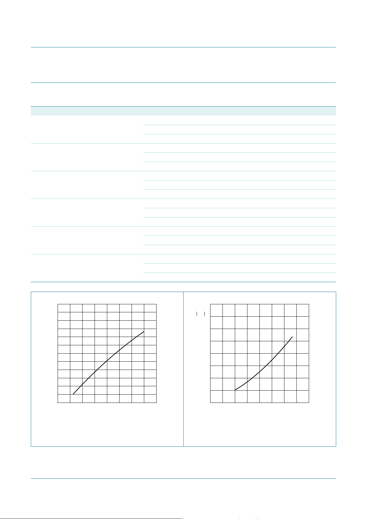
VDS = 15 V; Tj = 25 C. VDS = 15 V; VGS = 0 V; Tj = 25 C.
Fig 2. Drain current as a function of gate-source
cut-off voltage; typical values.
Fig 3. Forward transfer admittance as a function of
gate-source cut-off voltage; typical values.
BF545A_BF545B_BF545C All information provided in this document is subject to legal disclaimers. © NXP B.V. 2011. All rights reserved.
Product data sheet Rev. 4 — 15 September 2011 5 of 16

NXP Semiconductors
V
GSoff
(V)
0 −8−6−2 −4
mbb465
40
20
60
80
Y
os
(μS)
0
V
GSoff
(V)
0 −8−6−2 −4
mbb464
100
200
300
R
DSon
(Ω)
0
VDS (V)
0161248
mbb462
2
4
6
I
D
(mA)
0
(1)
(2)
(3)
VGS (V)
−30−1−2
mbb463
2
4
6
I
D
(mA)
0
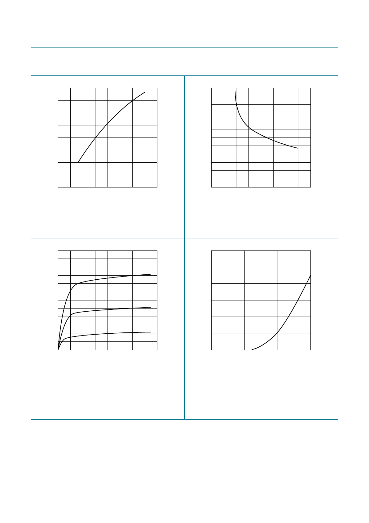
VDS = 15 V; VGS = 0 V; Tj = 25 C. VDS = 100 mV; VGS = 0 V; Tj = 25 C.
Fig 4. Common-source output admittance as a
function of gate-source cut-off voltage; typical
values.
BF545A; BF545B; BF545C
N-channel silicon junction field-effect transistors)
Fig 5. Drain-source on-resistance as a function of
gate-source cut-off voltage; typical values.
BF545A
T
j
(1) V
GS
(2) V
GS
(3) V
Fig 6. Typical output characteristics. Fig 7. Typical input characteristics.
BF545A_BF545B_BF545C All information provided in this document is subject to legal disclaimers. © NXP B.V. 2011. All rights reserved.
Product data sheet Rev. 4 — 15 September 2011 6 of 16
GS
= 25 C.
= 0 V.
= 0.5 V.
= 1.0 V.
BF545A
= 15 V; Tj = 25 C.
V
DS
 Loading...