

Page 1

AN12943
Spurious interrupt on MagniV
Rev. 0 — July, 2020
by: NXP Semiconductors
Contents
1 Introduction
The S12 MagniV family of microcontrollers includes single-die solutions that
are designed to provide a complete system-in-package (SiP) built on proven
S12 technology. With the integration of High-Voltage (HV) analog features into
a standard automotive MCU, the S12 MagniV family simplifies system design
by helping to improve manufacturing efficiency and reduce bill of materials
costs.
The S12Z CPU has taken advantage of this reduced need for absolute object
code compatibility to focus on improved support for C code-size efficiency and overall performance. The most obvious change
has been to eliminate the paged memory model and 64-kilobyte CPU addressing limitation of the CPU12 in favor of a linear 16megabyte address space. The X and Y index registers, as well as the stack pointer (SP) and program counter (PC), were
expanded from 16 bits to 24 bits to match the width of the address bus. The next biggest change has been to replace the 8-bit
A and B accumulators (sometimes used as the 16-bit D accumulator), with a set of eight general purpose data registers (Di ). D0
and D1 are 8 bits, D2 through D5 are 16 bits, and D6 and D7 are 32 bits.
1 Introduction ........................................... 1
2 S12Z features........................................ 1
3 Exceptions of S12Z................................2
4 Exception processing flow..................... 2
5 Solution to avoid spurious interrupt....... 4
6 Summary............................................... 4
Application Note
As in previous generations of CPU12, the S12Z CPU has variable-length instructions ranging from a single byte to several bytes.
The longest instructions in the CPU12 were moves with two extended addressing mode operand addresses (6 bytes of object
code). Moves could have indexed addressing mode operands, but only indexed modes that did not require additional extension
bytes. The S12Z CPU allows complete flexibility in specifying the addresses for move instructions so if both operands use an
indexed postbyte plus three extension bytes, these instructions can take up to nine bytes of object code. The longest instructions
in the S12Z CPU are the most complex math instructions (DIV, MAC, and MOD) which are page 2 opcodes plus a math postbyte
plus two operand addresses which could each be an addressing mode postbyte plus 3 extension bytes (11 bytes total).
The CPU12 used postbytes for indexed addressing, transfer/exchange, and looping primitive instructions. The S12Z CPU
instruction set has expanded the use of postbytes to improve code-size efficiency. The indexed postbyte was re-worked into a
general operand (OPR) addressing system. This new addressing mode postbyte includes indexed addressing modes like the
CPU12 and extended addressing modes, a quick-immediate mode, and register-as-memory addressing mode.
In addition to this general OPR addressing postbyte, the S12Z instruction set uses postbytes for transfer/exchange, looping
primitives, math (MUL, DIV, MAC, and MOD), relative addressing, shifts, bit-field instructions, and push/pull.
2 S12Z features
The S12Z CPU is the latest generation of CPU in the CPU12 line. This high-speed 16-bit processor has an expanded programmers
model with 24-bit wide X, Y, SP, and PC registers and replaces the A, B, and D accumulators with a set of eight general purpose
registers Di . Improved addressing modes support efficient use of the 16-megabyte (24-bit) linear address space.
• 24-Bit Linear Address Space (16-megabytes)
• 24-Bit Index Registers (X and Y), Stack Pointer (SP), and Program Counter (PC)
• Eight General Purpose Data Registers (D0, D1 8-Bits; D2–D5 16-Bits; D6, D7 32-Bits)
• Separate Memory Access Controllers for Code and Data
• Variable-Length Instructions Including Single-Byte and Odd Number of Bytes
• Extensive Use of Instruction Postbytes to Optimize Code-Size Efficiency
Page 2
NXP Semiconductors
Exceptions of S12Z
3 Exceptions of S12Z
Exceptions are events that require processing outside the normal flow of instruction execution. Central Processor Unit (CPU)
exceptions on the S12Z CPU include:
1. Reset
2. Software exceptions:
• Unimplemented page 1 opcode trap (SPARE)
• Unimplemented page 2 opcode trap (TRAP)
• Software interrupt instruction (SWI)
• System call interrupt instruction (SYS)
3. Machine exception
4. A non-maskable (X-bit) interrupt
5. Maskable (I-bit) interrupts
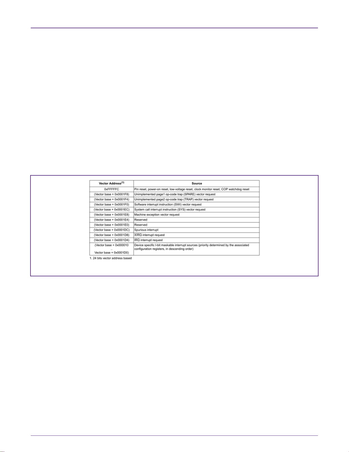
Each exception has an associated 24-bit vector, which points to the memory location where the routine that handles the exception
is located. The 24-bit exception vectors are taken from a vector table.
Figure 1. Example of exception vector map and priority
The S12Z CPU can handle up to 128 exception vectors, but the number actually used varies from device to device, and some
vectors are reserved for NXP use.
Exceptions can be classified into different categories, depending on the effect of the different ways to mask interrupts.
1. Reset.: This exception is not maskable.
2. Software exceptions: These include the unimplemented op-code traps, the SWI instruction and the SYS instruction.
Software exceptions are not maskable.
3. Machine exception: A machine exception cannot be masked. Sources for a machine exception are defined in the Memory
Map Control module (MMC). Please refer to the MMC chapter in the MCU ReferenceManual for details.
4. X-bit interrupt: The interrupt service requests from the XIRQ pin is handled as a X-bit interrupt. This exception can be
masked with the X-bit (X=1). The I-bit and the IPL-bits have no effect.
5. All remaining interrupt service requests can be masked with the I-bit (I=1) and are subject to priority filtering using the IPLbits.
4 Exception processing flow
The first cycle in the exception processing flow for all S12Z CPU exceptions is the same, regardless of the source of the exception.
Between the first and second cycles of execution, the CPU chooses one of four alternative paths. The first path is for reset, the
Spurious interrupt on MagniV, Rev. 0, July, 2020
Application Note 2 / 5
Page 3

NXP Semiconductors
Exception processing flow
second path is for machine exceptions, the third path is for pending hardware interrupts, and the fourth path is used for software
exceptions (SWI, SYS) and trapping unimplemented opcodes (SPARE, TRAP). The last two paths are virtually identical, differing
only in the details of calculating the return address. Refer to the below figure for the following description of events.
Figure 2. Exception processing flow diagram
For S12 MagniV family, it has INT module which decodes the priority of all system exception requests and provides the applicable
vector for processing the exception to the CPU. The INT module supports:
• Bit and X-bit maskable interrupt requests
• One non-maskable unimplemented page1 op-code trap
• One non-maskable unimplemented page2 op-code trap
• One non-maskable software interrupt (SWI)
• One non-maskable system call interrupt (SYS)
• One non-maskable machine exception vector request
• One spurious interrupt vector request
• One system reset vector request
Spurious interrupt on MagniV, Rev. 0, July, 2020
Application Note 3 / 5
Page 4

NXP Semiconductors
Solution to avoid spurious interrupt
The CPU handles both reset requests and interrupt requests. The INT module contains registers to configure the priority level of
each I-bit maskable interrupt request which can be used to implement an interrupt priority scheme. This also includes the
possibility to nest interrupt requests. A priority decoder is used to evaluate the relative priority of pending interrupt requests.
After system reset all I-bit maskable interrupt requests are configured to be enabled, are set up to be handled by the CPU and
have a pre-configured priority level of 1. Exceptions to this rule are the non-maskable interrupt requests and the spurious interrupt
vector request at (vector base + 0x0001DC) which cannot be disabled, are always handled by the CPU and have a fixed priority
levels. A priority level of 0 effectively disables the associated I-bit maskable interrupt request.
If more than one interrupt request is configured to the same interrupt priority level the interrupt request with the higher vector
address wins the prioritization.The following conditions must be met for an I-bit maskable interrupt request to be processed.
1. The local interrupt enabled bit in the peripheral module must be set.
2. The setup in the configuration register associated with the interrupt request channel must meet the following conditions:
a. The priority level must be set to non zero.
b. The priority level must be greater than the current interrupt processing level in the condition code register (CCW)
of the CPU (PRIOLVL[2:0] > IPL[2:0]).
3. The I-bit in the condition code register (CCW) of the CPU must be cleared.
4. There is no access violation interrupt request pending.
5. There is no SYS, SWI, SPARE, TRAP, Machine Exception or XIRQ request pending.
The INT module contains a priority decoder to determine the relative priority for all interrupt requests pending for the CPU.
A CPU interrupt vector is not supplied until the CPU requests it. Therefore, it is possible that a higher priority interrupt request
could override the original exception which caused the CPU to request the vector. In this case, the CPU will receive the highest
priority vector and the system will process this exception first instead of the original request.
If the interrupt source is unknown (for example, in the case where an interrupt request becomes inactive after the interrupt has
been recognized, but prior to the vector request), the vector address supplied to the CPU defaults to that of the spurious interrupt
vector.
User should ensure that all exception requests remain active until the system begins execution of the applicable service routine;
otherwise, the exception request may not get processed at all or the result may be a spurious interrupt request.
5 Solution to avoid spurious interrupt
The root cause for spurious interrupt is that the source of interrupt is unknown, where an interrupt request becomes inactive after
the interrupt has been recognized, but prior to the vector request. This kind of scenario is mostly happened with asynchronous
operation.
For example, in pump application, when the pump is switched off, it will disable the communication timer's interrupt. If exactly at
the time (which happens very rarely, likely in the first cycle in the exception processing flow of S12Z CPU), the corresponding
timer's interrupt is triggered. S12Z enters the exception processing flow. But the interrupt request becomes inactive and spurious
interrupt will be entered. To avoid such scenario, it's better to wait for another extra one period timer interrupt. After that interrupt,
disable this interrupt could be implemented immediately.
6 Summary
Spurious interrupt in S12Z family is a protective mechanism for unknown interrupt source and make CPU to run under predictable
action. The root cause to enter spurious interrupt is that an interrupt request becomes inactive after the interrupt has been
recognized, but prior to the vector request. Synchronous and sequential operation could make system much robust and lower
the possibility to enter protective mechanism of system.
Spurious interrupt on MagniV, Rev. 0, July, 2020
Application Note 4 / 5
Page 5

How To Reach Us
Home Page:
nxp.com
Web Support:
nxp.com/support
Information in this document is provided solely to enable system and software implementers to
use NXP products. There are no express or implied copyright licenses granted hereunder to
design or fabricate any integrated circuits based on the information in this document. NXP
reserves the right to make changes without further notice to any products herein.
NXP makes no warranty, representation, or guarantee regarding the suitability of its products for
any particular purpose, nor does NXP assume any liability arising out of the application or use
of any product or circuit, and specifically disclaims any and all liability, including without limitation
consequential or incidental damages. “Typical” parameters that may be provided in NXP data
sheets and/or specifications can and do vary in different applications, and actual performance
may vary over time. All operating parameters, including “typicals,” must be validated for each
customer application by customer's technical experts. NXP does not convey any license under
its patent rights nor the rights of others. NXP sells products pursuant to standard terms and
conditions of sale, which can be found at the following address: nxp.com/
SalesTermsandConditions.
While NXP has implemented advanced security features, all products may be subject to
unidentified vulnerabilities. Customers are responsible for the design and operation of their
applications and products to reduce the effect of these vulnerabilities on customer’s applications
and products, and NXP accepts no liability for any vulnerability that is discovered. Customers
should implement appropriate design and operating safeguards to minimize the risks associated
with their applications and products.
NXP, the NXP logo, NXP SECURE CONNECTIONS FOR A SMARTER WORLD, COOLFLUX,
EMBRACE, GREENCHIP, HITAG, I2C BUS, ICODE, JCOP, LIFE VIBES, MIFARE, MIFARE
CLASSIC, MIFARE DESFire, MIFARE PLUS, MIFARE FLEX, MANTIS, MIFARE ULTRALIGHT,
MIFARE4MOBILE, MIGLO, NTAG, ROADLINK, SMARTLX, SMARTMX, STARPLUG, TOPFET,
TRENCHMOS, UCODE, Freescale, the Freescale logo, AltiVec, C‑5, CodeTEST, CodeWarrior,
ColdFire, ColdFire+, C‑Ware, the Energy Efficient Solutions logo, Kinetis, Layerscape, MagniV,
mobileGT, PEG, PowerQUICC, Processor Expert, QorIQ, QorIQ Qonverge, Ready Play,
SafeAssure, the SafeAssure logo, StarCore, Symphony, VortiQa, Vybrid, Airfast, BeeKit,
BeeStack, CoreNet, Flexis, MXC, Platform in a Package, QUICC Engine, SMARTMOS, Tower,
TurboLink, and UMEMS are trademarks of NXP B.V. All other product or service names are the
property of their respective owners. AMBA, Arm, Arm7, Arm7TDMI, Arm9, Arm11, Artisan,
big.LITTLE, Cordio, CoreLink, CoreSight, Cortex, DesignStart, DynamIQ, Jazelle, Keil, Mali,
Mbed, Mbed Enabled, NEON, POP, RealView, SecurCore, Socrates, Thumb, TrustZone, ULINK,
ULINK2, ULINK-ME, ULINK-PLUS, ULINKpro, µVision, Versatile are trademarks or registered
trademarks of Arm Limited (or its subsidiaries) in the US and/or elsewhere. The related
technology may be protected by any or all of patents, copyrights, designs and trade secrets. All
rights reserved. Oracle and Java are registered trademarks of Oracle and/or its affiliates. The
Power Architecture and Power.org word marks and the Power and Power.org logos and related
marks are trademarks and service marks licensed by Power.org.
©
NXP B.V. 2020. All rights reserved.
For more information, please visit: http://www.nxp.com
For sales office addresses, please send an email to: salesaddresses@nxp.com
Date of release: July, 2020
Document identifier: AN12943
 Loading...