

Page 1

AN12868
Camera Interface in LPC55(S)xx
Rev. 1 — 10/2020
1 How to read this application note
This application note introduces a parallel interface for the camera solution
for LPC55(S)xx. It includes the introduction of camera interface, features and
API routines, and demo.
2 Target application
The camera interface can be used as important part of many camera usage
as below:
• Object detection
• Gesture recognition
• Color recognition
• QR code scanning, and so on
3 Introduction of camera interfaces
A typical camera interface supports at least one parallel interface, although
nowadays many camera interfaces begin to support the MIPI CSI interface.
The camera interface's parallel interface consists of the following lines:
• Data line (D[0:11]):
These are parallel data lines that carry pixel data. The data transmitted on
these lines change with every Pixel Clock (PCLK).
Application Note
Contents
1 How to read this application note.... 1
2 Target application............................1
3 Introduction of camera interfaces....1
4 Features of camera interface.......... 1
5 Function description........................ 2
5.1 Camera interface engine............. 2
5.2 Camera driver library................... 2
5.3 LCD display..................................2
5.4 System clock................................2
5.5 Clock source of camera............... 2
5.6 I2C interface................................. 2
5.7 Memory usage............................. 2
5.8 Other supported camera modules
.....................................................2
6 Pin description.................................3
6.1 Connection of interface................4
6.2 Requirement of interface............. 4
7 Library and API routine................... 4
7.1 Library..........................................4
7.2 API routine................................... 4
7.3 API routine description.................5
7.4 Code detail description................ 5
8 Demonstration.................................7
9 Revision history...............................8
A Purchasing LCD module used in this
demo............................................... 8
• Horizontal Sync (HSYNC)
This is a special signal that goes from the camera sensor. An HSYNC indicates that one line of the frame is transmitted.
• Vertical Sync (VSYNC)
This signal is transmitted after the entire frame is transferred. This signal is often a way to indicate that one entire frame
is transmitted.
• Pixel Clock (PCLK)
This is the pixel clock and it changes on every pixel.
The application note only focuses on Digital-Video-Port (DVP) interface which is parallel interface.
4 Features of camera interface
• Supported formats (8-bit): RGB565
• Maximum image transfer rate: 30 fps for QVGA(320 × 240). For small RAM parts, reduce the size of image and frame
rate.
Page 2

NXP Semiconductors
Function description
• Camera module tested : OV7673
• Other camera modules can be supported as long as they provide the same signal timing.
5 Function description
5.1 Camera interface engine
There is a hidden co-processor in LPC55S69 which can handle the signals of camera.
It reads the data from camera and stores the data in the RAM which can then be accessed by ARM core. Before using the
co-processor, some configurations need to be made, which includes pin configuration, clock enable, processor enable, interrupt
enable and so on.
5.2 Camera driver library
The instructions of co-processor use the type of machine code. The code implements the function of camera interface protocol
and is released in lib. Some API routines are provided in this application. User can use API routines to initialize the engine and
configure the pins.
5.3 LCD display
The application note uses LCD to display the video stream from camera in real time. The high-speed SPI port is used for LCD
driving port. The max speed on the SPI bus is 50 Mbps, so it can display the 320 × 240 resolution LCD up to 30 fps.
5.4 System clock
The camera engine shares the system clock with Arm® core. To speed up the processing time, the system clock must be
configured to 150 MHz. For those below 150 MHz, such as, 96 MHz system clock part, reduce the frequency of pixel clock.
5.5 Clock source of camera
The camera needs a 50 MHz clock source which can be provided by CLKOUT signal from MCU.
5.6 I2C interface
The camera is configured through I2C interface which can be connected with I2C peripheral port in the MCU.
5.7 Memory usage
The 320 × 240 resolution picture requires 150 K bytes RAM space. The solution uses the space address from 0x20010000
to 0x20035800.
Additionally, the instruction codes of camera engine need be run in the RAM for high performance. This solution uses the space
address from 0x20040000 to 0x20043FFF to store camera engine code.
5.8 Other supported camera modules
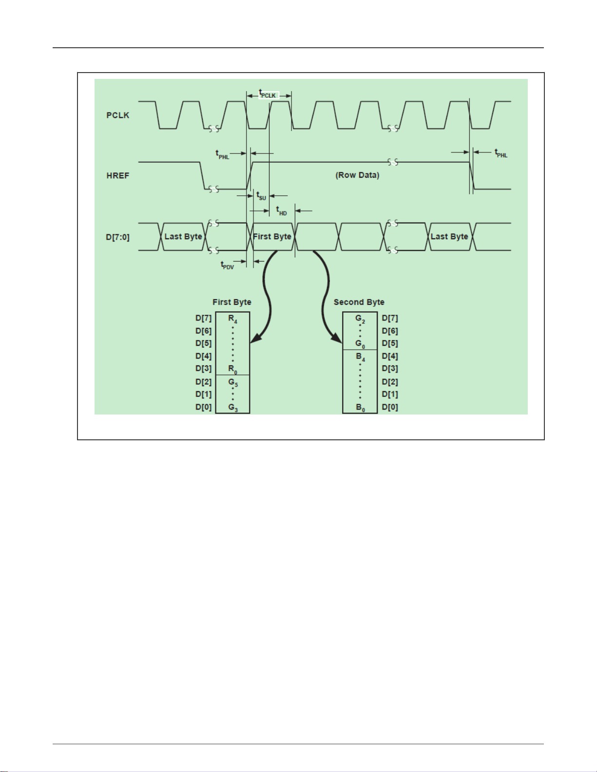
Other camera modules can be supported as long as they provide the same signal timing.
1. The camera module need to be configured as RGB565 mode with the timing diagram, as shown in Figure 1.
Camera Interface in LPC55(S)xx, Rev. 1, 10/2020
Application Note 2 / 9
Page 3
NXP Semiconductors
Pin description
Figure 1. Camera module configuration
2. The resolution should be configured as QVGA (320 × 240).
6 Pin description
Camera Interface in LPC55(S)xx, Rev. 1, 10/2020
Application Note 3 / 9
Page 4

NXP Semiconductors
6.1 Connection of interface
Library and API routine
Figure 2. Connection of interface
6.2 Requirement of interface
• The D0-D7 must be connected to P0.0-P0.7 for byte reading the data.
• SIOC and SIOD must be connected to the I2C interface of MCU for configuration.
• The VSYNC, HREF, PCLK must be connected to pins of Port0.
• XCLK needs to be connected to a clock output pin of MCU.
7 Library and API routine
7.1 Library
The library is named by camera engine lib. It includes the instructions which will be handled by co-processor.
The library can support Keil, MCUXpresso IDE, but not IAR.
7.2 API routine
The main purposes of the API routines include:
• Enable the clock of engine.
• Configure the IO as camera interface function.
• Initial the I2C interface.
• Enable the interrupt of engine for telling the Arm core data is ready.
Camera Interface in LPC55(S)xx, Rev. 1, 10/2020
Application Note 4 / 9
Page 5

NXP Semiconductors
• Initialize and start the engine.
7.3 API routine description
Table 1. API routine
Routine Description
Reserved46_IRQHandler Interrupt routine for camera engine
OV7670_Init Camera module initialization
Camera_Init(); Camera engine initialization
Camera_Start(); Camera engine start running
LCD_Init(); LCD module initialization
LCD_Refresh(); LCD refresh
7.4 Code detail description
7.4.1 System clock
Library and API routine
Camera engine need short time to store the data when every pixel edge comes. If the clock frequency of engine is higher, the time
cost is shorter. In this solution, the system clock must be set at 150MHz when engine is running. The code to configure system
clock is shown as below:
BOARD_BootClockPLL150M();
7.4.2 I2C interface
The flexcomm4 is used as I2C function for initializing the Camera before the video starts.
7.4.3 Pin function
Table 2. Pin function
Pin Function number Input/output Description
P0_0 15 Input Camera engine function
P0_1 15 Input Camera engine function
P0_2 15 Input Camera engine function
P0_3 15 Input Camera engine function
P0_4 15 Input Camera engine function
P0_5 15 Input Camera engine function
P0_6 15 Input Camera engine function
P0_7 15 Input Camera engine function
P0_18 15 Output Camera engine function
p0_13 0 Input GPIO as VSYNC input
P0_15 0 Input GPIO as Pixel clock input
Table continues on the next page...
Camera Interface in LPC55(S)xx, Rev. 1, 10/2020
Application Note 5 / 9
Page 6

NXP Semiconductors
Table 2. Pin function (continued)
Pin Function number Input/output Description
P0_16 2 Output CLKOUT
P1_20 5 Input/output FC4_I2C_SCL
P1_21 5 Output FC4_I2C_SDA
P1_2 6 Output LSPI_HS_SCK
P0_26 9 Output LSPI_HS_MOSI
P1_3 6 Input LSPI_HS_MISO
P1_1 5 Output LSPI_HS_SSEL1
Library and API routine
p1_11
P0_29 1 Input FC0_USART_RX
P0_30 1 Output FC0_USART_TX
0 Output GPIO
From P0_0 to P0_7 are the low eight bits, they can be read by engine at one read instruction which only takes one system
clock cycle.
P0_18 is set as camera engine function. It can be operated by engine directly such as set logic high level, clear zero, toggle and
so on. P0_18 will be toggled by engine after every VSYNC edge.
P0_13 and P0_15 are input function pins which can receive the VSYNC and pixel signals. The Pixel clock is 1/4 of clock source,
it is 12.5 Mhz.
As clock output pin, P0_16 will provide 50 MHz clock to camera as its clock source.
The LSPI_HS is high speed SPI interface which will be used to drive the LCD TFT screen.
7.4.4 LCD function
LCD is used to display the video of camera in real time. High-speed SPI is used to drive the LCD. The routine named by
LCD_Refresh() is a very high efficiency routine, it can refresh a 320 × 240 picture in about 24 ms, up to 40 fps. The bus clock of
high speed SPI can reach up to 50 MHz. The DMA isn’t used to drive the LCD. Instead, only software is used to drive LCD where
the Arm core writes the SPI FIFO data write register once it is empty.
Figure 3. LCD function
Camera Interface in LPC55(S)xx, Rev. 1, 10/2020
Application Note 6 / 9
Page 7

NXP Semiconductors
Demonstration
7.4.5 OV7670 camera module
The camera module is set as QVGA RGB565 mode. The 16-bit data will be received with two pixel edges (high-byte first and
low-byte follows).
At the beginning, the MCU initializes the camera through I2C interface. Then, the video stream data will be stored in the RAM by
camera engine.
7.4.6 Reserved 46_IRQHandler
Same with other peripheral handler, camera engine handler will be implemented by Arm core when engine finishes the
storage operation.
In the handler, a flag will be set as one. In the while(1) routine, the refreshing operation can be allowed when flag turns to
logic one.
7.4.7 Data buffer
There needs 150 KB space for one frame of video and LPC55S59 has about 300 KB RAM space. Double buffer isn’t possible.
Only one buffer is used. Because the LCD refresh time (24 ms) is shorted than data storage time (33 ms), so Arm always reads
the data for LCD refresh is earlier than storage operation by engine. Therefore, the media data won’t be lost.
7.4.8 Timing
The LCD always displays the previous frame data from the camera. Before displaying, the data stored needs to be optimized by
co-processor for exchanging the high and low bytes of every pixel. Because the speed of LCD module displaying is higher than the
speed of camera interface reading data, the single data buffer is used in this application. While the current frame data is stored,
the LCD displays the previous frame data.
8 Demonstration
1. Build and compile the project.
2. Plug one side of USB cable in PC USB port and another side in the debug link port in the EVK board, and then
download the image in the MCU.
3. Connect camera to MCU by referring to connection of interface in Chapter 4.
4. Connect the LCD panel with Arduino port on the LPCXpresso55s69 EVK board.
5. Connect one side of USB cable to USB power socket and the other to 5 V Power only USB port P5.
6. The LCD will display the video frame from camera as shown in Figure 4.
Camera Interface in LPC55(S)xx, Rev. 1, 10/2020
Application Note 7 / 9
Page 8

NXP Semiconductors
Revision history
Figure 4. Video frame
9 Revision history
Table 3. Revision history
Rev. Date Description
0 05/2020 Initial release
1 10/2020 Replaced LPC55(S)xx for LPC55S69
A Purchasing LCD module used in this demo
Purchase the LCD board at these links:
• https://www.waveshare.com/2.8inch-tft-touch-shield.htm
• http://www.waveshare.net/shop/2.8inch-TFT-Touch-Shield.htm
Camera Interface in LPC55(S)xx, Rev. 1, 10/2020
Application Note 8 / 9
Page 9

How To Reach Us
Home Page:
nxp.com
Web Support:
nxp.com/support
Information in this document is provided solely to enable system and software implementers
to use NXP products. There are no express or implied copyright licenses granted hereunder
to design or fabricate any integrated circuits based on the information in this document. NXP
reserves the right to make changes without further notice to any products herein.
NXP makes no warranty, representation, or guarantee regarding the suitability of its products
for any particular purpose, nor does NXP assume any liability arising out of the application
or use of any product or circuit, and specifically disclaims any and all liability, including
without limitation consequential or incidental damages. “Typical” parameters that may be
provided in NXP data sheets and/or specifications can and do vary in different applications,
and actual performance may vary over time. All operating parameters, including “typicals,”
must be validated for each customer application by customer's technical experts. NXP does
not convey any license under its patent rights nor the rights of others. NXP sells products
pursuant to standard terms and conditions of sale, which can be found at the following address:
nxp.com/SalesTermsandConditions.
While NXP has implemented advanced security features, all products may be subject to
unidentified vulnerabilities. Customers are responsible for the design and operation of their
applications and products to reduce the effect of these vulnerabilities on customer’s applications
and products, and NXP accepts no liability for any vulnerability that is discovered. Customers
should implement appropriate design and operating safeguards to minimize the risks associated
with their applications and products.
NXP, the NXP logo, NXP SECURE CONNECTIONS FOR A SMARTER WORLD, COOLFLUX,
EMBRACE, GREENCHIP, HITAG, I2C BUS, ICODE, JCOP, LIFE VIBES, MIFARE, MIFARE
CLASSIC, MIFARE DESFire, MIFARE PLUS, MIFARE FLEX, MANTIS, MIFARE ULTRALIGHT,
MIFARE4MOBILE, MIGLO, NTAG, ROADLINK, SMARTLX, SMARTMX, STARPLUG, TOPFET,
TRENCHMOS, UCODE, Freescale, the Freescale logo, AltiVec, C‑5, CodeTEST, CodeWarrior,
ColdFire, ColdFire+, C‑Ware, the Energy Efficient Solutions logo, Kinetis, Layerscape, MagniV,
mobileGT, PEG, PowerQUICC, Processor Expert, QorIQ, QorIQ Qonverge, Ready Play,
SafeAssure, the SafeAssure logo, StarCore, Symphony, VortiQa, Vybrid, Airfast, BeeKit,
BeeStack, CoreNet, Flexis, MXC, Platform in a Package, QUICC Engine, SMARTMOS, Tower,
TurboLink, UMEMS, EdgeScale, EdgeLock, eIQ, and Immersive3D are trademarks of NXP
B.V. All other product or service names are the property of their respective owners. AMBA,
Arm, Arm7, Arm7TDMI, Arm9, Arm11, Artisan, big.LITTLE, Cordio, CoreLink, CoreSight, Cortex,
DesignStart, DynamIQ, Jazelle, Keil, Mali, Mbed, Mbed Enabled, NEON, POP, RealView,
SecurCore, Socrates, Thumb, TrustZone, ULINK, ULINK2, ULINK-ME, ULINK-PLUS, ULINKpro,
µVision, Versatile are trademarks or registered trademarks of Arm Limited (or its subsidiaries)
in the US and/or elsewhere. The related technology may be protected by any or all of patents,
copyrights, designs and trade secrets. All rights reserved. Oracle and Java are registered
trademarks of Oracle and/or its affiliates. The Power Architecture and Power.org word marks and
the Power and Power.org logos and related marks are trademarks and service marks licensed
by Power.org.
©
NXP B.V. 2020. All rights reserved.
For more information, please visit: http://www.nxp.com
For sales office addresses, please send an email to: salesaddresses@nxp.com
Date of release: 10/2020
Document identifier: AN12868
 Loading...