

Page 1

35FS4500, 35FS6500: ASIL B
Grade 0 safety power system basis chip with CAN FD
transceiver
Rev. 2 — 14 April 2021 Product short data sheet
1 General description
The 35FS4500/35FS6500 ASIL B SMARTMOS devices are a multi-output, power
supply, integrated circuit, including CAN Flexible Data (FD) transceiver, dedicated to the
automotive market.
Multiple switching and linear voltage regulators, including low-power mode (32 μA) are
available with various wake-up capabilities. An advanced power management scheme
is implemented to maintain high efficiency over a wide range of input voltages (down to
2.7 V) and output current ranges (up to 1.5 A).
The 35FS4500/35FS6500 ASIL B includes configurable fail-safe/fail silent safety
behavior and features, with two fail-safe outputs, becoming a full part of a safety oriented
system partitioning, to reach a high integrity safety level (up to ASIL B).
The built-in CAN FD interface fulfills the ISO 11898-2
(11)
and -5
(12)
standards.
High temperature capability up to TA = 150 °C and TJ = 175 °C, compliant with AECQ100 Grade 0 automotive qualification.
2 Features and benefits
• Battery voltage sensing and MUX output pin
• Highly flexible SMPS pre-regulator, allowing two topologies: non-inverting buck-boost
and standard buck
• Family of devices to supply MCU core from 1.0 V to 5.0 V, with SMPS (0.8 A or 1.5 A)
or LDO (0.5 A)
• Linear voltage regulator dedicated to auxiliary functions, or to sensor supply (V
tracker or independent), 5.0 V, or 3.3 V
• Linear voltage regulator dedicated to MCU Analog/Digital (A/D) reference voltage or
I/Os supply (V
• 3.3 V keep alive memory supply available in low-power mode
• Long duration timer, counting up to 6 months with 1.0 s resolution
• Multiple wake-up sources in low-power mode: CAN, IOs, LDT
• Five configurable I/Os
3 Applications
• TA up to 150 °C and TJ up to 175 °C
• Drive Train Electrification (BMS, Hybrid EV and HEV, Inverter, DC-DC, Alterno Starter)
• Drive Train - Chassis and Safety (Active Suspension, Steering, Safety Domain
Gateway)
• Power Train (EMS, TCU, Gear Box)
• ADAS (LDW, Radar, Sensor Fusion Safety area)
), 5.0 V, or 3.3 V
CCA
CCA
Page 2
NXP Semiconductors
G
AT
E
_
L
S
V
P
R
E
S
W
_
CO
R
E
BO
O
T
_
C
O
R
E
V
CO
R
E
_
S
N
S
FB_COR E
COMP_CORE
FCRBM
VCCA_ E
VCCA_ B
VDDIO
VCCA
MUX_OUT
IO_5/VKA M
MOSI
MISO
SCLK
NCS
INTB
RSTB
TXD
RXD
IO_2
IO_3
BO
O
T
_
P
R
E
SW
_
P
R
E
2
SW
_
P
R
E
1
VS
UP
2
VS
UP
1
VSUP3
VSENSE
VAUX_E
VAUX_B
VAUX
SELECT
CAN-5 V
DEBUG
IO_0
IO_4
CANH
CANL
VPU-F S
+batter y
(KL30)
DEBUG
mode
ignition key
(KL15)
to switch
CAN BUS
fail-s afe
delay
fail-s afe
drive
V
AUX
V
PRE
V
DDIO
V
PRE
V
CORE
VDD
AD ref.
voltage
ADC Input
Vstandby
SPI
NMI
Reset
CAN
MCU
V
CCA
V
DDIO
V
CORE
or
V
CCA
FS1B
FS0B
GNDA DGNDGND_COM
35FS65 00C
aaa-03 9989
Grade 0 safety power system basis chip with CAN FD transceiver
• On board charger
• Motor control
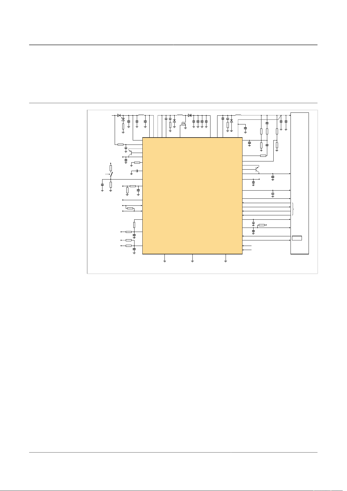
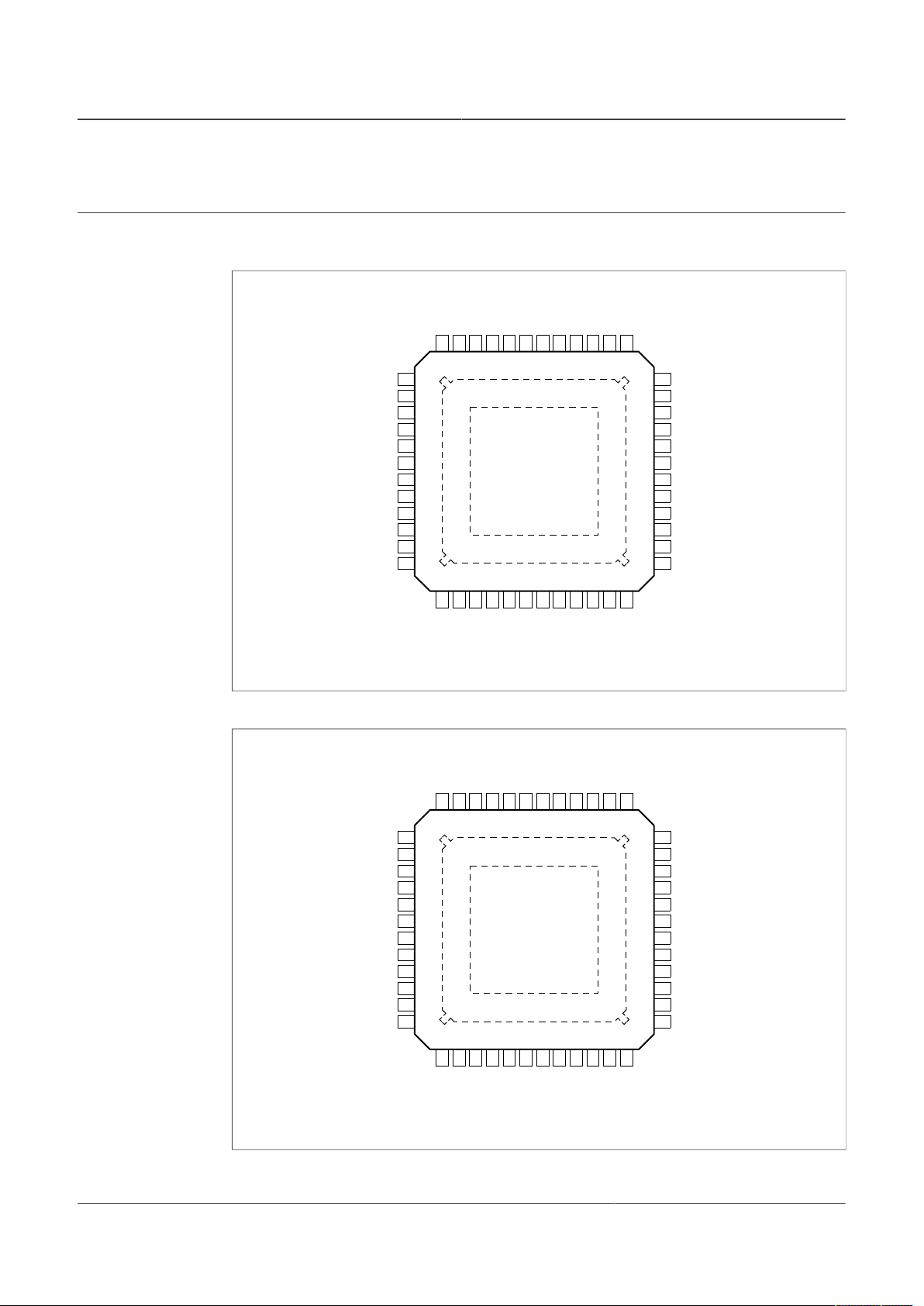
4 Simplified application diagrams
35FS4500, 35FS6500: ASIL B
Figure 1. 35FS6500C simplified application diagram - buck boost configuration - FS1B
35FS4500-35FS6500SDS-ASILB All information provided in this document is subject to legal disclaimers. © NXP B.V. 2021. All rights reserved.
Product short data sheet Rev. 2 — 14 April 2021
2 / 24
Page 3
NXP Semiconductors
aaa-039990
G
A
TE
_
L
S
V
P
R
E
S
W_
C
O
R
E
B
OO
T_
C
O
R
E
V
C
O
R
E
_
S
N
S
FB_CORE
COMP_CORE
FCRBM
VCCA_E
VCCA_B
VDDIO
VCCA
MUX_OUT
IO_5/VKAM
MOSI
MISO
SCLK
NCS
INTB
RSTB
TXD
RXD
IO_2
IO_3
B
OO
T_
P
R
E
S
W_
P
R
E
2
S
W_
P
R
E
1
V
S
U
P
2
V
S
U
P
1
VSUP3
VSENSE
VAUX_E
VAUX_B
VAUX
SELECT
CAN-5V
DEBUG
IO_0
IO_4
CANH
CANL
VPU-FS
+battery
(KL30)
DEBUG
mode
ignition key
(KL15)
to switch
CAN BUS
fail-safe
delay
fail-safe
drive
V
AUX
V
PRE
V
DDIO
V
PRE
V
CORE
VDD
AD ref.
voltage
ADC Input
Vstandby
SPI
NMI
Reset
CAN
MCU
V
CCA
V
DDIO
V
CORE
or
V
CCA
FS1B
FS0B
GNDA DGNDGND_COM
35FS4500C
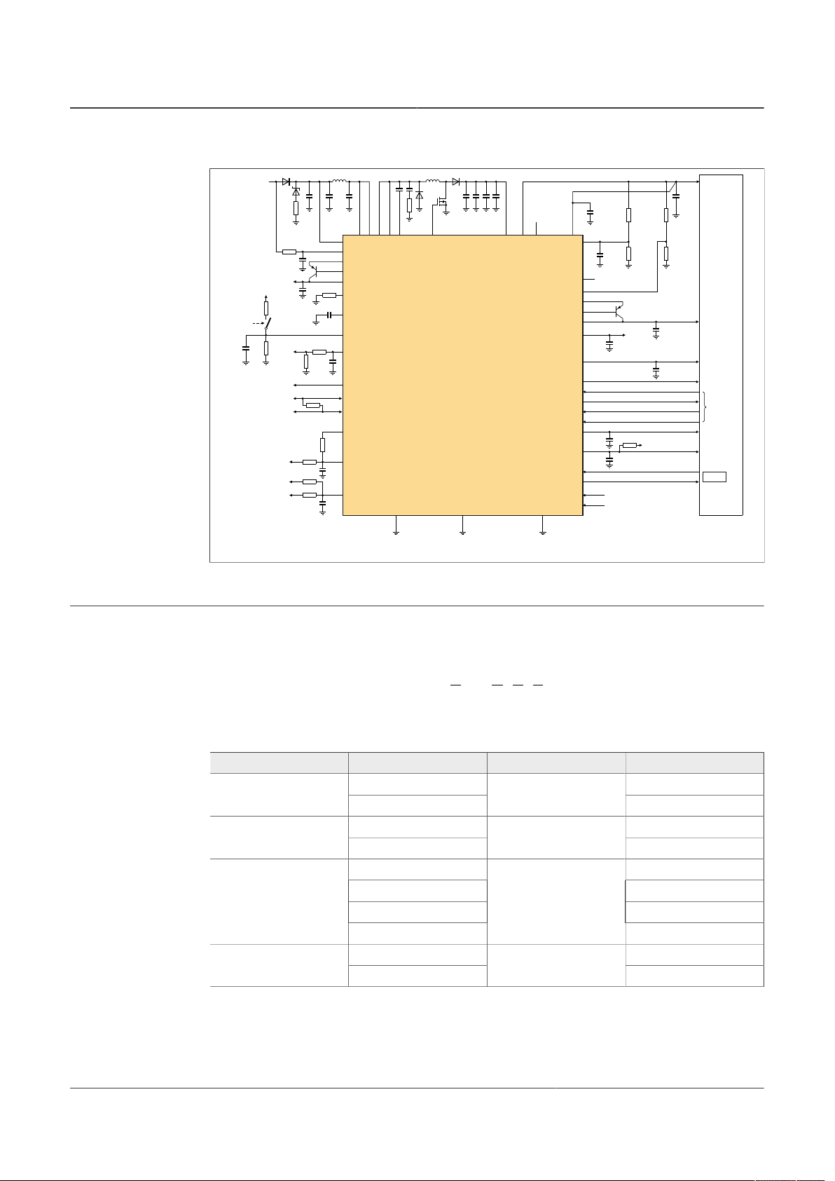
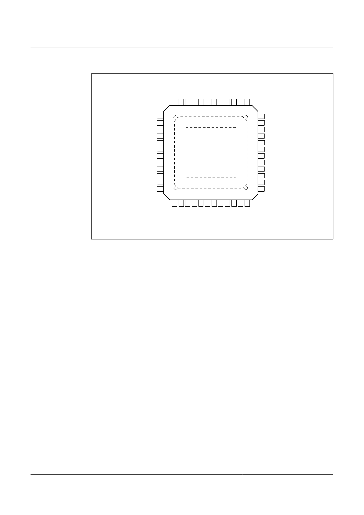
35FS4500, 35FS6500: ASIL B
Grade 0 safety power system basis chip with CAN FD transceiver
Figure 2. 35FS4500C simplified application diagram - buck boost configuration - FS1B
5 Ordering information
5.1 Part number definition
MC35FS c 5 x y z AE/R2
Table 1. Part number breakdown
Code Option Variable Description
4 series Linearc
6 series
35FS4500-35FS6500SDS-ASILB All information provided in this document is subject to legal disclaimers. © NXP B.V. 2021. All rights reserved.
Product short data sheet Rev. 2 — 14 April 2021
y
0 0.5 A or 0.8 Ax
1
5 None
6 FS1B
7 LDT
8
N Nonez
C
V
type
CORE
V
current
CORE
Functions
Physical interface
FS1B and LDT
DC-DC
1.5 A
CAN FD
3 / 24
Page 4
NXP Semiconductors
35FS4500, 35FS6500: ASIL B
Grade 0 safety power system basis chip with CAN FD transceiver
5.2 Part numbers list
Table 2. Orderable part variations
Part Number Temperature
MC35FS4505NAE 0 0 0.5 A Linear by SPI 0 B
MC35FS4505CAE 0 0 0.5 A Linear by SPI 1 B
MC35FS4506NAE 1 0 0.5 A Linear by SPI 0 B
MC35FS4506CAE 1 0 0.5 A Linear by SPI 1 B
MC35FS4507NAE 0 1 0.5 A Linear by SPI 0 B
MC35FS4507CAE 0 1 0.5 A Linear by SPI 1 B
MC35FS4508NAE 1 1 0.5 A Linear by SPI 0 B
MC35FS4508CAE 1 1 0.5 A Linear by SPI 1 B
MC35FS6505NAE 0 0 0.8 A DC-DC by SPI 0 B
MC35FS6505CAE 0 0 0.8 A DC-DC by SPI 1 B
MC35FS6506NAE 1 0 0.8 A DC-DC by SPI 0 B
MC35FS6506CAE 1 0 0.8 A DC-DC by SPI 1 B
MC35FS6507NAE 0 1 0.8 A DC-DC by SPI 0 B
MC35FS6507CAE 0 1 0.8 A DC-DC by SPI 1 B
MC35FS6508NAE 1 1 0.8 A DC-DC by SPI 0 B
MC35FS6508CAE 1 1 0.8 A DC-DC by SPI 1 B
MC35FS6515NAE 0 0 1.5 A DC-DC by SPI 0 B
MC35FS6515CAE 0 0 1.5 A DC-DC by SPI 1 B
MC35FS6516NAE 1 0 1.5 A DC-DC by SPI 0 B
MC35FS6516CAE 1 0 1.5 A DC-DC by SPI 1 B
MC35FS6517NAE 0 1 1.5 A DC-DC by SPI 0 B
MC35FS6517CAE 0 1 1.5 A DC-DC by SPI 1 B
MC35FS6518NAE 1 1 1.5 A DC-DC by SPI 0 B
MC35FS6518CAE
(TA)
–40 °C to
150 °C
Package FS1B LDT VCORE VCORE
type
48-pin LQFP
exposed pad
1 1 1.5 A DC-DC by SPI 1 B
VKAM On CANFDASIL Notes
[1]
[1] To order parts in tape and reel, add the R2 suffix to the part number.
35FS4500-35FS6500SDS-ASILB All information provided in this document is subject to legal disclaimers. © NXP B.V. 2021. All rights reserved.
Product short data sheet Rev. 2 — 14 April 2021
4 / 24
Page 5
NXP Semiconductors
aaa-037810
VSUP3
VSUP1
VSUP2
SW_PRE1
SW_PRE2
BOOT_PRE
GATE_LS
VPRE
DGND
Vpre
Vpre
Vpre
Vpre
Vpre
select
select
debug
debug
MIFO_FS
Vsup3
Vsup3
(1)
Vsup3
Vsup3Vpre
Vpre
Vpre
Vsup3
Vsup_mon
Vsense_mon
CAN diag
Vpre
Vsense
Vref
(2.5 V)
SW_CORE
FB_CORE
VCORE_SNS
BOOT_CORE
COMP_CORE
VCCA_E
VCCA_B
VCCA
GNDA
MUX_OUT
DEBUG
INTB
NCS
SCLK
MOSI
MISO
VDDIO
VSENSE
RXD
TXD
RSTB
FS0B
FS1B
VPU_FS
VAUX_E
VAUX_B
VAUX
CAN-5V
SELECT
IO_0
IO_0
IO_2
IO_3
IO_4
IO_5/VKAM
VKAM
FCRBM
CANH
CANL
GND_COM
Vpre SMPS
TSD
Vaux LINEAR REGULATOR
TSD
TSD
Vcore SMPS
Vcca LINEAR REGULATOR
ANALOG
REFERENCE #1
POWER
MANAGEMENT
STATE
MACHINE
LONG
DURATION
TIMER
TSD
TSD
CHARGE
PUMP
V2p5d
MAIN
V2p5d
FS
OSC
MAIN
VKAM
SPI
MAIN
MUX
INTERFACE
Vcan
LINEAR REGULATOR
CAN-5 V
CAN-5 V
FB_core
Vaux Vcca
Die
Temp
I/Os
INTERFACE
(1)
(1)
SPI
FS
OSC
FS
ANALOG REFERENCE #2
FS
CAN FLEXIBLE DATA INTERFACE
(1)
fail safe logic and supply
part number dependent
(1)
VOLTAGE
REGULATOR
SUPERVISOR
(OVER AND
UNDERVOLTAGE)
FAIL SAFE
MACHINE
FS1B DELAY
AND DRIVER
5
5
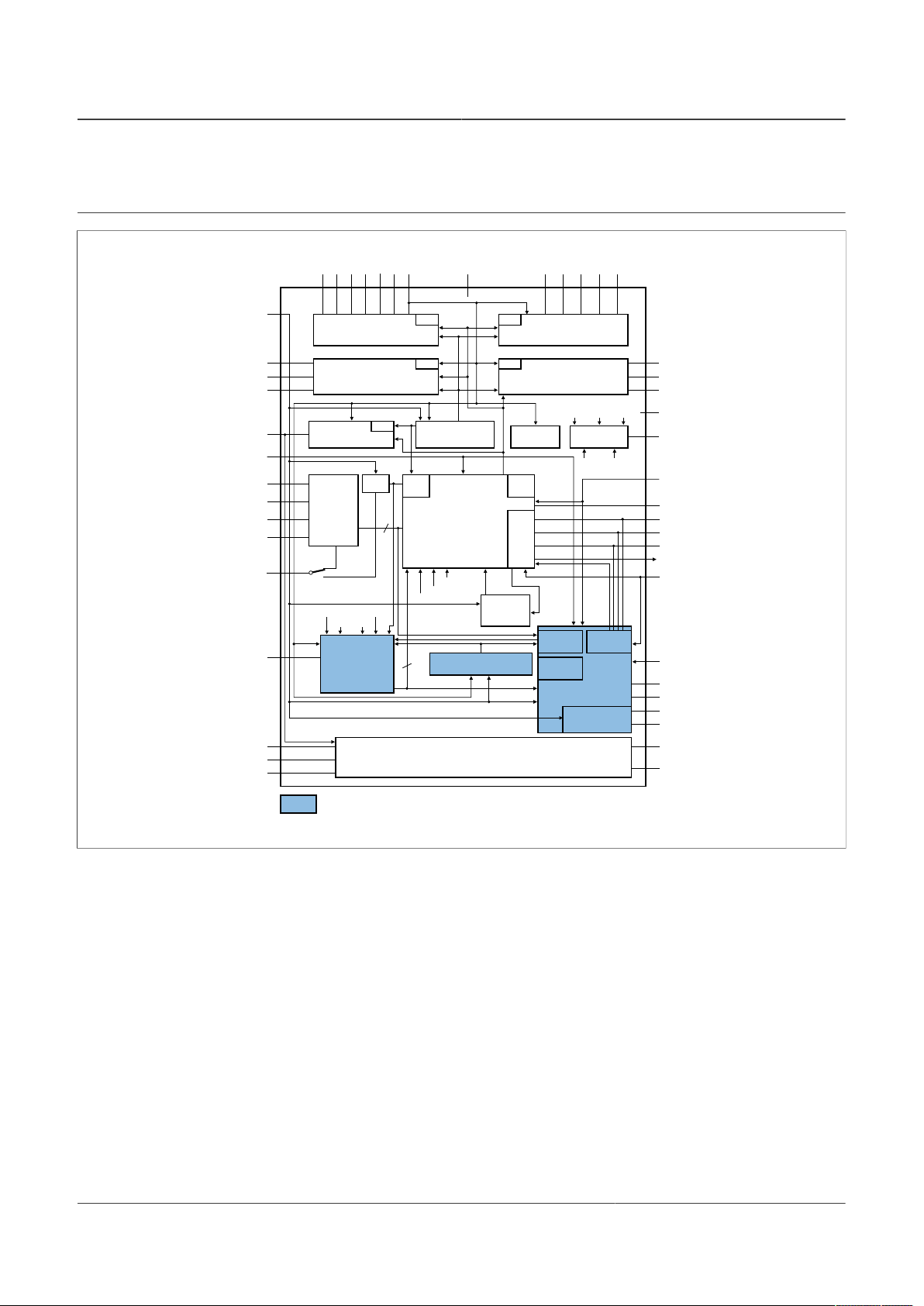
6 Block diagram
35FS4500, 35FS6500: ASIL B
Grade 0 safety power system basis chip with CAN FD transceiver
Figure 3. 35FS4500/35FS6500 with CAN simplified internal block diagram
35FS4500-35FS6500SDS-ASILB All information provided in this document is subject to legal disclaimers. © NXP B.V. 2021. All rights reserved.
Product short data sheet Rev. 2 — 14 April 2021
5 / 24
Page 6
NXP Semiconductors
VSUP1 BOOT_CORE
VSUP2 SW_CORE
VSENSE VCORE _SNS
VSUP3 COMP_CORE
FS1B FB_CORE
GND_C OM SELECT
CAN_ 5V VDDIO
CANH INTB
CANL NCS
IO_4 SCLK
IO_5/ VK AM MOSI
IO_0 MISO
FCRBM
S
W
_
P
R
E
1
FS0B
S
W
_
P
R
E
2
DE
BUG
B
O
O
T
_
P
R
E
AGND
DG
N
D
MUX _OUT
GA
T
E
_
L
S
IO_2
V
C
C
A
IO_3
V
C
C
A
_
B
TXD
V
C
C
A
_
E
RXD
VA
U
X
_
E
VP
U_FS
VA
U
X
_
B
n.c
.
RSTB
VA
U
X
VP
R
E
aaa- 03773 4
1
2
3
4
5
6
7
8
9
10
11
12
36
35
34
33
32
31
30
29
28
27
26
25
131415161718192021
22
23
48
4
7
464544
43
4
241
403938
3
724
VSUP1 BOOT_CORE
VSUP2 SW_CORE
VSENSE VCORE _SNS
VSUP3 COMP_CORE
n.c. FB_CORE
GND_C OM SELECT
CAN_ 5V VDDIO
n.c INTB
n.c NCS
IO_4 SCLK
IO_5/ VK AM MOSI
IO_0 MISO
FCRBM
S
W
_
P
R
E
1
FS0B
S
W
_
P
R
E
2
DE
BUG
B
O
O
T
_
P
R
E
AGND
DG
N
D
MUX _OUT
GA
T
E
_
L
S
IO_2
V
C
C
A
IO_3
V
C
C
A
_
B
n.c.
V
C
C
A
_
E
n.c
.
VA
U
X
_
E
n.c
.
VA
U
X
_
B
n.c
.
RSTB
VA
U
X
VP
R
E
aaa- 03773 6
1
2
3
4
5
6
7
8
9
10
11
12
36
35
34
33
32
31
30
29
28
27
26
25
131415161718192021
22
23
48
4
7
464544
43
4
241
403938
3
724
7 Pinning information
7.1 Pinning information
35FS4500, 35FS6500: ASIL B
Grade 0 safety power system basis chip with CAN FD transceiver
Figure 4. 35FS6500 pinout with CAN and FS1B
Figure 5. 35FS6500 pinout without CAN
35FS4500-35FS6500SDS-ASILB All information provided in this document is subject to legal disclaimers. © NXP B.V. 2021. All rights reserved.
Product short data sheet Rev. 2 — 14 April 2021
6 / 24
Page 7
NXP Semiconductors
VSUP1 n.c.
VSUP2 VCORE
VSENSE VCORE _SNS
VSUP3 n.c.
FS1B FB_CORE
GND_C OM SELECT
CAN_ 5V VDDIO
CANH INTB
CANL NCS
IO_4 SCLK
IO_5/ VK AM MOSI
IO_0 MISO
FCRBM
S
W
_
P
R
E
1
FS0B
S
W
_
P
R
E
2
DE
BUG
B
O
O
T
_
P
R
E
AGND
DG
N
D
GA
T
E
_
L
S
IO_2
V
C
C
A
IO_3
V
C
C
A
_
B
TXD
V
C
C
A
_
E
RXD
VA
U
X
_
E
VP
U_FS VA
U
X
_
B
n.c.
RSTB
VA
U
X
VP
R
E
aaa- 037737
1
2
3
4
5
6
7
8
9
10
11
12
36
35
34
33
32
31
30
29
28
27
26
25
131415161718192021
22
23
48
4
7
464544
43
4
241
403938
3
724
35FS4500, 35FS6500: ASIL B
Grade 0 safety power system basis chip with CAN FD transceiver
Figure 6. 35FS4500 pinout with CAN and FS1B
35FS4500-35FS6500SDS-ASILB All information provided in this document is subject to legal disclaimers. © NXP B.V. 2021. All rights reserved.
Product short data sheet Rev. 2 — 14 April 2021
7 / 24
Page 8
NXP Semiconductors
35FS4500, 35FS6500: ASIL B
Grade 0 safety power system basis chip with CAN FD transceiver
7.2 Pin description
A functional description of each pin can be found in the full data sheet.
Table 3. 35FS4500/35FS6500 pin definition
Pin
number
1 VSUP1 A_IN Power supply of the device. An external reverse battery protection diode in series is
2 VSUP2 A_IN Second power supply. Protected by the external reverse battery protection diode
3 VSENSE A_IN Sensing of the battery voltage. Must be connected prior to the reverse battery
4 VSUP3 A_IN Third power supply dedicated to the device supply. Protected by the external
5 FS1B D_OUT Second output of the safety block (active low). The pin is asserted low at start-up
6 GND_COM GROUND Dedicated ground for physical layers
7 CAN_5V A_OUT Output voltage for the embedded CAN FD interface
8 CANH A_IN/OUT CAN output high. If CAN function is not used, this pin must be left open.
9 CANL A_IN/OUT CAN output low. If CAN function is not used, this pin must be left open.
10 IO_4 D_IN
11 IO_5/VKAM A_IN
12 IO_0 A_IN
13 FCRBM A_IN Feedback core resistor bridge monitoring: For safety purposes, this pin is used to
14 FS0B D_OUT First output of the safety block (active low). The pin is asserted low at start-up and
Pin name Type Definition
mandatory
used for VSUP1. VSUP1 and VSUP2 must be connected together externally.
protection diode.
reverse battery protection diode used for VSUP1. Must be connected between the
reverse protection diode and the input PI filter.
and when a fault condition is detected, with a configurable delay or duration versus
FS0B output terminal. Open drain structure.
Can be used as digital input (load dump proof) with wake-up capability or as an
A_OUT
D_IN
A_OUT
D_IN
output gate driver
Digital input: Pin status can be read through the SPI. Can be used to monitor error
signals from another IC for safety purposes (when used with IO_5).
Wake-up capability: Can be selectable to wake-up on edges or levels.
Output gate driver: Can drive a logic level low-side NMOS transistor. Controlled by
the SPI.
Can be used as digital input with wake-up capability or as an analog output
providing keep alive memory supply in low-power mode.
Analog input: Pin status can be read through the MUX output terminal
Digital input: Pin status can be read through the SPI. Can be used to monitor error
signals from another IC for safety purposes (when used with IO_4).
Wake-up capability: Can be selectable to wake-up on edges or levels.
Supply output: Provide keep alive memory supply in low-power mode
Can be used as analog or digital input (load dump proof) with wake-up capability
(selectable)
Analog input: Pin status can be read through the MUX output terminal
Digital input: Pin status can be read through the SPI.
Wake-up capability: Can be selectable to wake-up on edges or levels.
monitor the middle point of a redundant resistor bridge connected on V
parallel to the one used to set the V
connected directly to FB_CORE.
when a fault condition is detected. Open drain structure.
voltage). If not used, this pin must be
CORE
CORE
(in
35FS4500-35FS6500SDS-ASILB All information provided in this document is subject to legal disclaimers. © NXP B.V. 2021. All rights reserved.
Product short data sheet Rev. 2 — 14 April 2021
8 / 24
Page 9

NXP Semiconductors
35FS4500, 35FS6500: ASIL B
Grade 0 safety power system basis chip with CAN FD transceiver
Table 3. 35FS4500/35FS6500 pin definition...continued
Pin
number
15 DEBUG D_IN Debug mode entry input
16 AGND GROUND Analog ground connection
17 MUX_OUT A_OUT Multiplexed output to be connected to a MCU ADC. Selection of the analog
18
19
20 TXD D_IN Transceiver input from the MCU which controls the state of the CAN-bus. Internal
21 RXD D_OUT Receiver output which reports the state of the CAN-bus to the MCU
22 VPU_FS A_OUT Pull-up output for FS1B function. If FS1B function is not used, this pin must be left
23 NC N/A Not connected. Pin must be left open.
24 RSTB D_OUT This output is asserted low when the safety block reports a failure. The main
25 MISO D_OUT SPI bus. Master input slave output
26 MOSI D_IN SPI bus. Master output slave input
27 SCLK D_IN SPI Bus. Serial clock
28 NCS D_IN Not chip select (active low)
29 INTB D_OUT This output pin generates a low pulse when an Interrupt condition occurs. Pulse
30 VDDIO A_IN Input voltage for MISO output buffer. Allows voltage compatibility with MCU I/Os.
31 SELECT D_IN Hardware selection pin for VAUX and VCCA output voltages
32 FB_CORE A_IN VCORE voltage feedback. Input of the error amplifier.
33 COMP_
34 VCORE_
36 BOOT_
37 VPRE A_IN VPRE input voltage sense
38 VAUX A_OUT VAUX output voltage. External PNP ballast transistor. Collector connection
39 VAUX_B A_OUT VAUX voltage regulator. External PNP ballast transistor. Base connection
40 VAUX_E A_OUT VAUX voltage regulator. External PNP ballast transistor. Emitter connection
41 VCCA_E A_OUT VCCA voltage regulator. External PNP ballast transistor. Emitter connection
35FS4500-35FS6500SDS-ASILB All information provided in this document is subject to legal disclaimers. © NXP B.V. 2021. All rights reserved.
Product short data sheet Rev. 2 — 14 April 2021
Pin name Type Definition
parameter is available at MUX-OUT through the SPI.
IO_2:3 D_IN Digital input pin with wake-up capability (logic level compatible)
Digital input: Pin status can be read through the SPI.
Wake-up capability: Can be selectable to wake-up on edges or levels.
pull-up to VDDIO.
If CAN function is not used, this pin must be left open.
If CAN function is not used, this pin must be left open.
open.
function is to reset the MCU. Reset input voltage is also monitored in order to detect
external reset and fault condition. Open drain structure.
duration is configurable. Internal pull-up to VDDIO.
A_OUT Compensation network. Output of the error amplifier.
CORE
A_IN VCORE input voltage sense
SNS
SW_CORE A_OUT VCORE output switching point for FS6500 series35
or VCORE A_OUT VCORE output voltage for FS4500 series
A_IN/OUT Bootstrap capacitor for VCORE internal NMOS gate drive
CORE
For FS4500 series, this pin must be left open (NC).
For FS4500 series, this pin must be left open (NC).
9 / 24
Page 10

NXP Semiconductors
35FS4500, 35FS6500: ASIL B
Grade 0 safety power system basis chip with CAN FD transceiver
Table 3. 35FS4500/35FS6500 pin definition...continued
Pin
Pin name Type Definition
number
42 VCCA_B A_OUT VCCA voltage regulator. External PNP ballast transistor. Base connection
43 VCCA A_OUT VCCA output voltage. External PNP ballast transistor. Collector connection
44 GATE_LS A_OUT Low-side MOSFET gate drive for non-inverting buck-boost configuration
45 DGND GROUND Digital ground connection
46 BOOT_PRE A_IN/OUT Bootstrap capacitor for the VPRE internal NMOS gate drive
47 SW_PRE2 A_OUT Second pre-regulator output switching point
48 SW_PRE1 A_OUT First pre-regulator output switching point
8 Maximum ratings
Table 4. Maximum ratings
All voltages are with respect to ground, unless otherwise specified. Exceeding these ratings may cause a malfunction or permanent damage
to the device.
Symbol Ratings Value Unit Notes
Electrical ratings
V
SUP1/2/3
V
SENSE
V
SW1,2
V
PRE
V
GATE_LS
V
BOOT_PRE
V
SW_CORE
V
CORE_SNS
V
BOOT_CORE
V
FB_CORE
V
COMP_CORE
V
FCRBM
V
AUX_B,E
V
AUX
V
CCA_B,E
V
CCA
V
DDIO
V
CAN_5V
V
PU_FS
V
FSxB
V
DEBUG
V
IO_0,4
V
IO_5
V
KAM
DC voltage at power supply pins –1.0 to 40 V
DC voltage at battery sense pin (with ext R in series mandatory) –14 to 40 V
DC voltage at SW_PRE1 and SW_PRE2 Pins –1.0 to 40 V
DC voltage at VPRE Pin –0.3 to 8 V
DC voltage at Gate_LS pin –0.3 to 8 V
DC voltage at BOOT_PRE pin –1.0 to 50 V
DC voltage at SW_CORE pin –1.0 to 8 V
DC voltage at VCORE_SNS pin 0.0 to 8 V
DC voltage at BOOT_CORE pin 0.0 to 15 V
DC voltage at FB_CORE pin –0.3 to 2.5 V
DC voltage at COMP_CORE pin –0.3 to 2.5 V
DC voltage at FCRBM pin –0.3 to 8 V
DC voltage at VAUX_B, VAUX_E pins –0.3 to 40 V
DC voltage at VAUX pin –2.0 to 40 V
DC voltage at VCCA_B, VCCA_E pins –0.3 to 8 V
DC voltage at VCCA pin –0.3 to 8 V
DC voltage at VDDIO pin –0.3 to 8 V
DC voltage on CAN_5V pin –0.3 to 8 V
DC voltage at VPU_FS pin –0.3 to 8 V
DC voltage at FS0B, FS1B pins (with ext R in series mandatory) –0.3 to 40 V
DC voltage at DEBUG pin –0.3 to 40 V
DC voltage at IO_0, IO_4 pins (with ext R in series mandatory) –0.3 to 40 V
DC voltage at IO_5 pin –0.3 to 20 V
DC voltage at VKAM pin –0.3 to 8 V
[1]
35FS4500-35FS6500SDS-ASILB All information provided in this document is subject to legal disclaimers. © NXP B.V. 2021. All rights reserved.
Product short data sheet Rev. 2 — 14 April 2021
10 / 24
Page 11

NXP Semiconductors
35FS4500, 35FS6500: ASIL B
Grade 0 safety power system basis chip with CAN FD transceiver
Table 4. Maximum ratings ...continued
All voltages are with respect to ground, unless otherwise specified. Exceeding these ratings may cause a malfunction or permanent damage
to the device.
Symbol Ratings Value Unit Notes
V
DIG
V
SELECT
V
BUS_CAN
I_Isense V
I_IO
0, 4, 5
ESD voltage
Human body model (JESD22/A114)
V
ESD-HBM1
V
ESD-HBM2
V
ESD-HBM3
Charge device model (JESD22/C101)
V
ESD-CDM1
V
ESD-CDM2
System level ESD (gun test)
V
ESD-GUN1
V
ESD-GUN2
V
ESD-GUN3
V
ESD-GUN4
V
ESD-GUN5
V
ESD-GUN6
V
ESD-GUN7
V
ESD-GUN8
Thermal ratings
T
A
T
J
T
STG
Thermal resistance
R
θJA
R
θJCTOP
R
θJCBOTTOM
DC voltage at INTB, RSTB, MISO, MOSI, NCS, SCLK, MUX_OUT, RXD, TXD, IO_2,
–0.3 to 8 V
IO_3 pins
DC voltage at SELECT pin –0.3 to 8 V
DC voltage on CANL, CANH pins –27 to 40 V
maximum current capability –5.0 to 5.0 mA
SENSE
IOs maximum current capability (IO_0, IO_4, IO_5) –5.0 to 5.0 mA
(18)
– 100 pF, 1.5 kΩ
• All pins ±2.0 kV
• VSUP1, 2, 3, VSENSE, VAUX, IO_0,4, FS0B, FS1B, DEBUG ±4.0 kV
• CANH, CANL ±6.0 kV
(19)
:
• All pins ±500 V
• Corner pins ±750 V
• VSUP1, 2, 3, VSENSE, VAUX, IO_0, 4, 5, FS0B, FS1B
330 Ω/150 pF unpowered according to IEC 61000-4-2:
(15)
±8.0 kV
330 Ω/150 pF unpowered according to OEM LIN, CAN, FlexRay Conformance ±8.0 kV
2.0 kΩ/150 pF unpowered according to ISO 10605
2.0 kΩ/330 pF powered according to ISO 10605
(14)
(14)
±8.0 kV
±8.0 kV
• CANH, CANL
330 Ω/150 pF unpowered according to IEC 61000-4-2:
(15)
±15.0 kV
330 Ω/150 pF unpowered according to OEM LIN, CAN, FlexRay Conformance ±12.0 kV
2.0 kΩ/150 pF unpowered according to ISO 10605
2.0 kΩ/330 pF powered according to ISO 10605
(14)
(14)
±15.0 kV
±12.0 kV
Ambient temperature –40 to 150 °C
Junction temperature –40 to 175 °C
Storage temperature –55 to 150 °C
Thermal resistance junction to ambient 30 °C/W
Thermal resistance junction to case top 23.8 °C/W
Thermal resistance junction to case bottom 0.9 °C/W
[2]
[3]
[4]
[5]
[1] All V
[2] Compared to AGND.
[3]
[4]
[5] Thermal resistance between the die and the solder pad on the bottom of the packaged based on simulation without any interface resistance.
35FS4500-35FS6500SDS-ASILB All information provided in this document is subject to legal disclaimers. © NXP B.V. 2021. All rights reserved.
SUPS (VSUP1/2/3
Per JEDEC JESD51-6
Thermal resistance between the die and the case top surface as measured by the cold plate method (MIL SPEC - 883 Method 1012.1)
) must be connected to the same supply (Figure 1).
(16)
with the board (JESD51-7)
(17)
horizontal.
(20)
.
Product short data sheet Rev. 2 — 14 April 2021
11 / 24
Page 12

NXP Semiconductors
35FS4500, 35FS6500: ASIL B
Grade 0 safety power system basis chip with CAN FD transceiver
9 Packaging
9.1 Package mechanical dimensions
Package dimensions are provided in package drawings. To find the most current package
outline drawing, go to www.nxp.com and perform a keyword search for the drawing’s
document number.
Table 5. Package mechanical dimensions
Package Suffix Package outline drawing number
7.0 × 7.0, 48–Pin LQFP exposed pad,
with 0.5 mm pitch, and a 4.5 × 4.5
exposed pad
AE 98ASA00173D
35FS4500-35FS6500SDS-ASILB All information provided in this document is subject to legal disclaimers. © NXP B.V. 2021. All rights reserved.
Product short data sheet Rev. 2 — 14 April 2021
12 / 24
Page 13

NXP Semiconductors
9.2 Package outline
35FS4500, 35FS6500: ASIL B
Grade 0 safety power system basis chip with CAN FD transceiver
Figure 7. SOT1571-1 Rev F
35FS4500-35FS6500SDS-ASILB All information provided in this document is subject to legal disclaimers. © NXP B.V. 2021. All rights reserved.
Product short data sheet Rev. 2 — 14 April 2021
13 / 24
Page 14

NXP Semiconductors
35FS4500, 35FS6500: ASIL B
Grade 0 safety power system basis chip with CAN FD transceiver
Figure 8. SOT1571-1 Rev. F Detail View
35FS4500-35FS6500SDS-ASILB All information provided in this document is subject to legal disclaimers. © NXP B.V. 2021. All rights reserved.
Product short data sheet Rev. 2 — 14 April 2021
14 / 24
Page 15

NXP Semiconductors
35FS4500, 35FS6500: ASIL B
Grade 0 safety power system basis chip with CAN FD transceiver
Figure 9. SOT1571-1 Rev F Notes
35FS4500-35FS6500SDS-ASILB All information provided in this document is subject to legal disclaimers. © NXP B.V. 2021. All rights reserved.
Product short data sheet Rev. 2 — 14 April 2021
15 / 24
Page 16

NXP Semiconductors
10 Soldering
35FS4500, 35FS6500: ASIL B
Grade 0 safety power system basis chip with CAN FD transceiver
Figure 10. SOT1571-1 Rev. F - PCB design guidelines - solder mask opening pattern
35FS4500-35FS6500SDS-ASILB All information provided in this document is subject to legal disclaimers. © NXP B.V. 2021. All rights reserved.
Product short data sheet Rev. 2 — 14 April 2021
16 / 24
Page 17

NXP Semiconductors
35FS4500, 35FS6500: ASIL B
Grade 0 safety power system basis chip with CAN FD transceiver
Figure 11. SOT1571-1 Rev. F - PCB design guidelines - I/O pads and solderable area
35FS4500-35FS6500SDS-ASILB All information provided in this document is subject to legal disclaimers. © NXP B.V. 2021. All rights reserved.
Product short data sheet Rev. 2 — 14 April 2021
17 / 24
Page 18

NXP Semiconductors
35FS4500, 35FS6500: ASIL B
Grade 0 safety power system basis chip with CAN FD transceiver
Figure 12. SOT1571-1 Rev. F - PCB design guidelines - solder paste stencil
35FS4500-35FS6500SDS-ASILB All information provided in this document is subject to legal disclaimers. © NXP B.V. 2021. All rights reserved.
Product short data sheet Rev. 2 — 14 April 2021
18 / 24
Page 19

NXP Semiconductors
35FS4500, 35FS6500: ASIL B
Grade 0 safety power system basis chip with CAN FD transceiver
11 References
Obtain additional information on related NXP products and application solutions through
the documents and URLs listed below.
(1) AN5238 - FS6500 and FS4500 Safe System Basis Chip Hardware Design and Product Guidelines - Application Note
https://www.nxp.com/AN5238-DOWNLOAD
(2) AN4388 - Quad Flat Package (QFP)
https://www.nxp.com/files/analog/doc/app_note/AN4388.pdf
(3) FS6500-FS4500PDTCALC - Power dissipation tool (Excel File)
https://www.nxp.com/files/analog/software_tools/FS6500-FS4500-power-dissipation-calculator.xlsx
(4) V
(5) FMEDA - FS6500/FS4500 ASILB Grade 0 FMEDA
(6) UM11548 - 35FS4500/35FS6500 functional safety manual – ASIL B – Safety manual
(7) KITFS4508CAEEVM - FS4508, System Basis Chip, ASIL B, Linear 0.5 A Vcore, FS1b, LDT, CAN
(8) FS6500 product summary page - https://www.nxp.com/FS6500
(9) FS4500 product summary page - https://www.nxp.com/FS4500
(10) Analog power management homepage - https://www.nxp.com/products/power-management
(11) ISO 11898-2:2003 - Road vehicles — Controller area network (CAN) — Part 2: High-speed medium access unit
(12) ISO 11898-5:2007 - Road vehicles — Controller area network (CAN) — Part 5: High-speed medium access unit with
(13) ISO 7637-2:2011 - Road vehicles — Electrical disturbances from conduction and coupling — Part 2: Electrical
(14) ISO 10605:2008 - Road vehicles — Test methods for electrical disturbances from electrostatic discharge
(15) IEC 61000-4-2:2008 - Electromagnetic compatibility (EMC) - Part 4-2: Testing and measurement techniques -
(16) JESD51- 6 - INTEGRATED CIRCUIT THERMAL TEST METHOD ENVIRONMENTAL CONDITIONS - FORCED
(17) JESD51-7 - HIGH EFFECTIVE THERMAL CONDUCTIVITY TEST BOARD FOR LEADED SURFACE MOUNT
(18) JESD22-A114F - ELECTROSTATIC DISCHARGE (ESD) SENSITIVITY TESTING HUMAN BODY MODEL (HBM)
(19) JESD22-C101F - FIELD-INDUCED CHARGED-DEVICE MODEL TEST METHOD FOR ELECTROSTATIC
(20) MIL-STD-883-1, Method 1012.1 - TEST METHOD STANDARD MICROCIRCUITS
compensation network simulation tool (CNC)
CORE
https://www.nxp.com/KITFS4508CAEEVM
https://www.iso.org/standard/33423.html
low-power mode
https://www.iso.org/contents/data/standard/04/12/41284.html
transient conduction along supply lines only
https://www.iso.org/standard/50925.html
https://www.iso.org/standard/41937.html
Electrostatic discharge immunity test
https://webstore.iec.ch/publication/4189
CONVECTION (MOVING AIR)
PACKAGES
DISCHARGE WITHSTAND THRESHOLDS OF MICROELECTRONIC COMPONENTS
[1]
[1]
[1] Available upon request.
35FS4500-35FS6500SDS-ASILB All information provided in this document is subject to legal disclaimers. © NXP B.V. 2021. All rights reserved.
Product short data sheet Rev. 2 — 14 April 2021
19 / 24
Page 20

NXP Semiconductors
35FS4500, 35FS6500: ASIL B
Grade 0 safety power system basis chip with CAN FD transceiver
12 Revision history
Table 6. Revision history
Document ID Release date Data sheet status Supersedes
35FS4500-35FS6500SDS-ASILB v.2.0 20210414 Product 35FS4500-35FS6500SDS-ASILB v.1.0
Modifications
35FS4500-35FS6500SDS-ASILB v.1.0 20210105 Product —
Modifications
• Section 1: replaced "0.8 A" by "1.5 A"
• Section 2: replaced "Family of devices to supply MCU core from 1.0 V to 5.0 V, with SMPS (0.8 A) or
LDO (0.5 A)" to "Family of devices to supply MCU core from 1.0 V to 5.0 V, with SMPS (0.8 A to 1.5 A) or
LDO (0.5 A)"
• Section 5: updated Table 1 and Table 2 (added new part numbers)
• Initial release
35FS4500-35FS6500SDS-ASILB All information provided in this document is subject to legal disclaimers. © NXP B.V. 2021. All rights reserved.
Product short data sheet Rev. 2 — 14 April 2021
20 / 24
Page 21

NXP Semiconductors
13 Legal information
13.1 Data sheet status
35FS4500, 35FS6500: ASIL B
Grade 0 safety power system basis chip with CAN FD transceiver
Document status
Objective [short] data sheet Development This document contains data from the objective specification for product
Preliminary [short] data sheet Qualification This document contains data from the preliminary specification.
Product [short] data sheet Production This document contains the product specification.
[1] Please consult the most recently issued document before initiating or completing a design.
[2] The term 'short data sheet' is explained in section "Definitions".
[3] The product status of device(s) described in this document may have changed since this document was published and may differ in case of multiple
devices. The latest product status information is available on the Internet at URL http://www.nxp.com.
[1][2]
Product status
13.2 Definitions
Draft — A draft status on a document indicates that the content is still
under internal review and subject to formal approval, which may result
in modifications or additions. NXP Semiconductors does not give any
representations or warranties as to the accuracy or completeness of
information included in a draft version of a document and shall have no
liability for the consequences of use of such information.
Short data sheet — A short data sheet is an extract from a full data sheet
with the same product type number(s) and title. A short data sheet is
intended for quick reference only and should not be relied upon to contain
detailed and full information. For detailed and full information see the
relevant full data sheet, which is available on request via the local NXP
Semiconductors sales office. In case of any inconsistency or conflict with the
short data sheet, the full data sheet shall prevail.
Product specification — The information and data provided in a Product
data sheet shall define the specification of the product as agreed between
NXP Semiconductors and its customer, unless NXP Semiconductors and
customer have explicitly agreed otherwise in writing. In no event however,
shall an agreement be valid in which the NXP Semiconductors product
is deemed to offer functions and qualities beyond those described in the
Product data sheet.
13.3 Disclaimers
Limited warranty and liability — Information in this document is believed
to be accurate and reliable. However, NXP Semiconductors does not
give any representations or warranties, expressed or implied, as to the
accuracy or completeness of such information and shall have no liability
for the consequences of use of such information. NXP Semiconductors
takes no responsibility for the content in this document if provided by an
information source outside of NXP Semiconductors. In no event shall NXP
Semiconductors be liable for any indirect, incidental, punitive, special or
consequential damages (including - without limitation - lost profits, lost
savings, business interruption, costs related to the removal or replacement
of any products or rework charges) whether or not such damages are based
on tort (including negligence), warranty, breach of contract or any other
legal theory. Notwithstanding any damages that customer might incur for
any reason whatsoever, NXP Semiconductors’ aggregate and cumulative
liability towards customer for the products described herein shall be limited
in accordance with the Terms and conditions of commercial sale of NXP
Semiconductors.
Right to make changes — NXP Semiconductors reserves the right to
make changes to information published in this document, including without
limitation specifications and product descriptions, at any time and without
[3]
Definition
development.
notice. This document supersedes and replaces all information supplied prior
to the publication hereof.
Applications — Applications that are described herein for any of these
products are for illustrative purposes only. NXP Semiconductors makes
no representation or warranty that such applications will be suitable
for the specified use without further testing or modification. Customers
are responsible for the design and operation of their applications and
products using NXP Semiconductors products, and NXP Semiconductors
accepts no liability for any assistance with applications or customer product
design. It is customer’s sole responsibility to determine whether the NXP
Semiconductors product is suitable and fit for the customer’s applications
and products planned, as well as for the planned application and use of
customer’s third party customer(s). Customers should provide appropriate
design and operating safeguards to minimize the risks associated with
their applications and products. NXP Semiconductors does not accept any
liability related to any default, damage, costs or problem which is based
on any weakness or default in the customer’s applications or products, or
the application or use by customer’s third party customer(s). Customer is
responsible for doing all necessary testing for the customer’s applications
and products using NXP Semiconductors products in order to avoid a
default of the applications and the products or of the application or use by
customer’s third party customer(s). NXP does not accept any liability in this
respect.
Limiting values — Stress above one or more limiting values (as defined in
the Absolute Maximum Ratings System of IEC 60134) will cause permanent
damage to the device. Limiting values are stress ratings only and (proper)
operation of the device at these or any other conditions above those
given in the Recommended operating conditions section (if present) or the
Characteristics sections of this document is not warranted. Constant or
repeated exposure to limiting values will permanently and irreversibly affect
the quality and reliability of the device.
Terms and conditions of commercial sale — NXP Semiconductors
products are sold subject to the general terms and conditions of commercial
sale, as published at http://www.nxp.com/profile/terms, unless otherwise
agreed in a valid written individual agreement. In case an individual
agreement is concluded only the terms and conditions of the respective
agreement shall apply. NXP Semiconductors hereby expressly objects to
applying the customer’s general terms and conditions with regard to the
purchase of NXP Semiconductors products by customer.
No offer to sell or license — Nothing in this document may be interpreted
or construed as an offer to sell products that is open for acceptance or
the grant, conveyance or implication of any license under any copyrights,
patents or other industrial or intellectual property rights.
Export control — This document as well as the item(s) described herein
may be subject to export control regulations. Export might require a prior
authorization from competent authorities.
35FS4500-35FS6500SDS-ASILB All information provided in this document is subject to legal disclaimers. © NXP B.V. 2021. All rights reserved.
Product short data sheet Rev. 2 — 14 April 2021
21 / 24
Page 22

NXP Semiconductors
35FS4500, 35FS6500: ASIL B
Grade 0 safety power system basis chip with CAN FD transceiver
Translations — A non-English (translated) version of a document is for
reference only. The English version shall prevail in case of any discrepancy
between the translated and English versions.
Security — Customer understands that all NXP products may be subject
to unidentified or documented vulnerabilities. Customer is responsible
for the design and operation of its applications and products throughout
their lifecycles to reduce the effect of these vulnerabilities on customer’s
applications and products. Customer’s responsibility also extends to other
open and/or proprietary technologies supported by NXP products for use
in customer’s applications. NXP accepts no liability for any vulnerability.
Customer should regularly check security updates from NXP and follow up
appropriately. Customer shall select products with security features that best
meet rules, regulations, and standards of the intended application and make
the ultimate design decisions regarding its products and is solely responsible
for compliance with all legal, regulatory, and security related requirements
concerning its products, regardless of any information or support that may
be provided by NXP. NXP has a Product Security Incident Response Team
(PSIRT) (reachable at PSIRT@nxp.com) that manages the investigation,
reporting, and solution release to security vulnerabilities of NXP products.
Suitability for use in automotive applications — This NXP product has
been qualified for use in automotive applications. It has been developed in
accordance with ISO 26262, and has been ASIL-classified accordingly. If
this product is used by customer in the development of, or for incorporation
into, products or services (a) used in safety critical applications or (b) in
which failure could lead to death, personal injury, or severe physical or
environmental damage (such products and services hereinafter referred
to as “Critical Applications”), then customer makes the ultimate design
decisions regarding its products and is solely responsible for compliance with
all legal, regulatory, safety, and security related requirements concerning
its products, regardless of any information or support that may be provided
by NXP. As such, customer assumes all risk related to use of any products
in Critical Applications and NXP and its suppliers shall not be liable for
any such use by customer. Accordingly, customer will indemnify and hold
NXP harmless from any claims, liabilities, damages and associated costs
and expenses (including attorneys’ fees) that NXP may incur related to
customer’s incorporation of any product in a Critical Application.
13.4 Trademarks
Notice: All referenced brands, product names, service names and
trademarks are the property of their respective owners.
NXP — wordmark and logo are trademarks of NXP B.V.
SafeAssure — is a trademark of NXP B.V.
35FS4500-35FS6500SDS-ASILB All information provided in this document is subject to legal disclaimers. © NXP B.V. 2021. All rights reserved.
Product short data sheet Rev. 2 — 14 April 2021
22 / 24
Page 23

NXP Semiconductors
Tables
35FS4500, 35FS6500: ASIL B
Grade 0 safety power system basis chip with CAN FD transceiver
Tab. 1. Part number breakdown ....................................3
Tab. 2. Orderable part variations ...................................4
Tab. 3. 35FS4500/35FS6500 pin definition ................... 8
Figures
Fig. 1. 35FS6500C simplified application diagram
- buck boost configuration - FS1B .....................2
Fig. 2. 35FS4500C simplified application diagram
- buck boost configuration - FS1B .....................3
Fig. 3. 35FS4500/35FS6500 with CAN simplified
internal block diagram ....................................... 5
Fig. 4. 35FS6500 pinout with CAN and FS1B .............. 6
Fig. 5. 35FS6500 pinout without CAN .......................... 6
Fig. 6. 35FS4500 pinout with CAN and FS1B .............. 7
Tab. 4. Maximum ratings ............................................. 10
Tab. 5. Package mechanical dimensions .................... 12
Tab. 6. Revision history ............................................... 20
Fig. 7. SOT1571-1 Rev F ...........................................13
Fig. 8. SOT1571-1 Rev. F Detail View ....................... 14
Fig. 9. SOT1571-1 Rev F Notes ................................ 15
Fig. 10. SOT1571-1 Rev. F - PCB design guidelines
- solder mask opening pattern ........................ 16
Fig. 11. SOT1571-1 Rev. F - PCB design guidelines
- I/O pads and solderable area ....................... 17
Fig. 12. SOT1571-1 Rev. F - PCB design guidelines
- solder paste stencil ....................................... 18
35FS4500-35FS6500SDS-ASILB All information provided in this document is subject to legal disclaimers. © NXP B.V. 2021. All rights reserved.
Product short data sheet Rev. 2 — 14 April 2021
23 / 24
Page 24

NXP Semiconductors
Grade 0 safety power system basis chip with CAN FD transceiver
Contents
1 General description ............................................ 1
2 Features and benefits ......................................... 1
3 Applications .........................................................1
4 Simplified application diagrams ........................ 2
5 Ordering information .......................................... 3
5.1 Part number definition ....................................... 3
5.2 Part numbers list ............................................... 4
6 Block diagram ..................................................... 5
7 Pinning information ............................................ 6
7.1 Pinning information ............................................ 6
7.2 Pin description ................................................... 8
8 Maximum ratings ...............................................10
9 Packaging .......................................................... 12
9.1 Package mechanical dimensions .................... 12
9.2 Package outline ............................................... 13
10 Soldering ............................................................16
11 References ......................................................... 19
12 Revision history ................................................ 20
13 Legal information .............................................. 21
35FS4500, 35FS6500: ASIL B
Please be aware that important notices concerning this document and the product(s)
described herein, have been included in section 'Legal information'.
© NXP B.V. 2021. All rights reserved.
For more information, please visit: http://www.nxp.com
For sales office addresses, please send an email to: salesaddresses@nxp.com
Document identifier: 35FS4500-35FS6500SDS-ASILB
Date of release: 14 April 2021
 Loading...