

NTE NTE5368, NTE5369 Datasheet

NTE5368 & NTE5369
Silicon Controlled Rectifier (SCR)
125 Amp
Absolute Maximum Ratings: (TJ = +125°C unless otherwise specified)
Repetitive Peak Voltages, V
NTE5368 600V. . . . . . . . . . . . . . . . . . . . . . . . . . . . . . . . . . . . . . . . . . . . . . . . . . . . . . . . . . . . . . . . . . .
NTE5369 1200V. . . . . . . . . . . . . . . . . . . . . . . . . . . . . . . . . . . . . . . . . . . . . . . . . . . . . . . . . . . . . . . . . .
Non–Repetitive Peak Reverse Blocking Voltage, V
NTE5368 700V. . . . . . . . . . . . . . . . . . . . . . . . . . . . . . . . . . . . . . . . . . . . . . . . . . . . . . . . . . . . . . . . . . .
NTE5369 1300V. . . . . . . . . . . . . . . . . . . . . . . . . . . . . . . . . . . . . . . . . . . . . . . . . . . . . . . . . . . . . . . . . .
Average On–State Current (Half Sine Wave, TC = +85°C), I
RMS On–State Current, I
T(RMS)
Continuous On–State Current, I
Peak One–Cycle Surge (10ms duration, 60% V
Non–Repetitive On–State Current (10ms duration, VR ≤ 10V), I
Maximum Permissible Surge Energy (VR ≤ 10V), I2t
10ms duration 13600A2s. . . . . . . . . . . . . . . . . . . . . . . . . . . . . . . . . . . . . . . . . . . . . . . . . . . . . . . . . .
3ms duration 10000A2s. . . . . . . . . . . . . . . . . . . . . . . . . . . . . . . . . . . . . . . . . . . . . . . . . . . . . . . . . . .
Peak Forward Gate Current (Anode positive with respect to cathode), I
Peak Forward Gate Voltage (Anode positive with respect to cathode), V
Peak Reverse Gate Voltage, V
Average Gate Power, P
G
Peak Gate Power (100µs pulse width), P
Rate of Rise of Off–State Voltage (To 80% V
Rate of Rise of On–State Current, di/dt
(Gate drive 20V, 20Ω with tr ≤ 1µs, anode voltage ≤ 80% V
Repetitive 500A/µs. . . . . . . . . . . . . . . . . . . . . . . . . . . . . . . . . . . . . . . . . . . . . . . . . . . . . . . . . . . .
Non–Repetitive 1000A/µs. . . . . . . . . . . . . . . . . . . . . . . . . . . . . . . . . . . . . . . . . . . . . . . . . . . . . .
Operating Temperature Range, T
Storage Temperature Range, T
Thermal Resistance, Junction–to–Case, R
(For a device with a maximum forward voltage drop characteristic) 0.23°C/W. . . . . . . . . . . .
RRM
, V
T
RGM
hs
stg
DRM
, V
DSM
GM
DRM
thJC
RSM
T(AV)
re–applied), I
RRM
TSM (1)
TSM (2)
FGM
gate open–circuit), dv/dt 200V/µs. . . . . . . . . . . . .
)
DRM
FGM
75A. . . . . . . . . . . . . . . . . . . . . . . . . .
175A. . . . . . . . . . . . . . . . . . . . . . . . . . . . . . . . . . . . . . . . . . . . . . . . . . . . .
175A. . . . . . . . . . . . . . . . . . . . . . . . . . . . . . . . . . . . . . . . . . . . . . . . . . . .
1500A. . . . . . . . . . . . . . . .
1650A. . . . . . . . . . . . . . . . . . .
14A. . . . . . . . . . . . . . . .
20V. . . . . . . . . . . . . . .
5V. . . . . . . . . . . . . . . . . . . . . . . . . . . . . . . . . . . . . . . . . . . . . . . . . . . .
1.5W. . . . . . . . . . . . . . . . . . . . . . . . . . . . . . . . . . . . . . . . . . . . . . . . . . . . . . . . . . .
60W. . . . . . . . . . . . . . . . . . . . . . . . . . . . . . . . . . . . . . . . . .
–40° to +125°C. . . . . . . . . . . . . . . . . . . . . . . . . . . . . . . . . . . . . . . . .
–40° to +150°C. . . . . . . . . . . . . . . . . . . . . . . . . . . . . . . . . . . . . . . . . .
Absolute Maximum Ratings (Cont’d): (TJ = +125°C unless otherwise specified)
Peak On–State Voltage (ITM = 280A), V
Forward Conduction Threshold Voltage, V
TM
O
Forward Conduction Slope Resistance, r 3mΩ. . . . . . . . . . . . . . . . . . . . . . . . . . . . . . . . . . . . . . . . . . . . .
Repetitive Peak Off–State Current (At V
Repetitive Peak Reverse Current (At V
Maximum Gate Current (V
Maximum Gate Voltage (V
= 6V, IA = 1A, TJ = +25°C), I
A
= 6V, IA = 1A, TJ = +25°C), V
A
Maximum Holding Current (VA = 6V, IA = 1A, TJ = +25°C), I
Maximum Gate Voltage Which Will Not Trigger Any Device, V
Typical Stored Charge (ITM = 200A, drR/dt = 10A/µs, VRM = 50V, 50% chord value), Q
Circuit Commutated Turn–Off Time (ITM = 200A, diR/dt = 10A/µs, VRM = 50V), t
(200V/µs to 80% V
(20V/µs to 80% V
)25–40µs. . . . . . . . . . . . . . . . . . . . . . . . . . . . . . . . . . . . . . . . . . . . . . . . . . .
DRM
) (typical) 20–35µs. . . . . . . . . . . . . . . . . . . . . . . . . . . . . . . . . . . . . . . . . . . .
DRM
DRM
RRM
), I
), I
DRM
RRM
GT
GT
200mA. . . . . . . . . . . . . . . . . . . . . . . . . . .
H
GD
q
600mA. . . . . . . . . . . . . . . . . . . . . . . . . .
rr
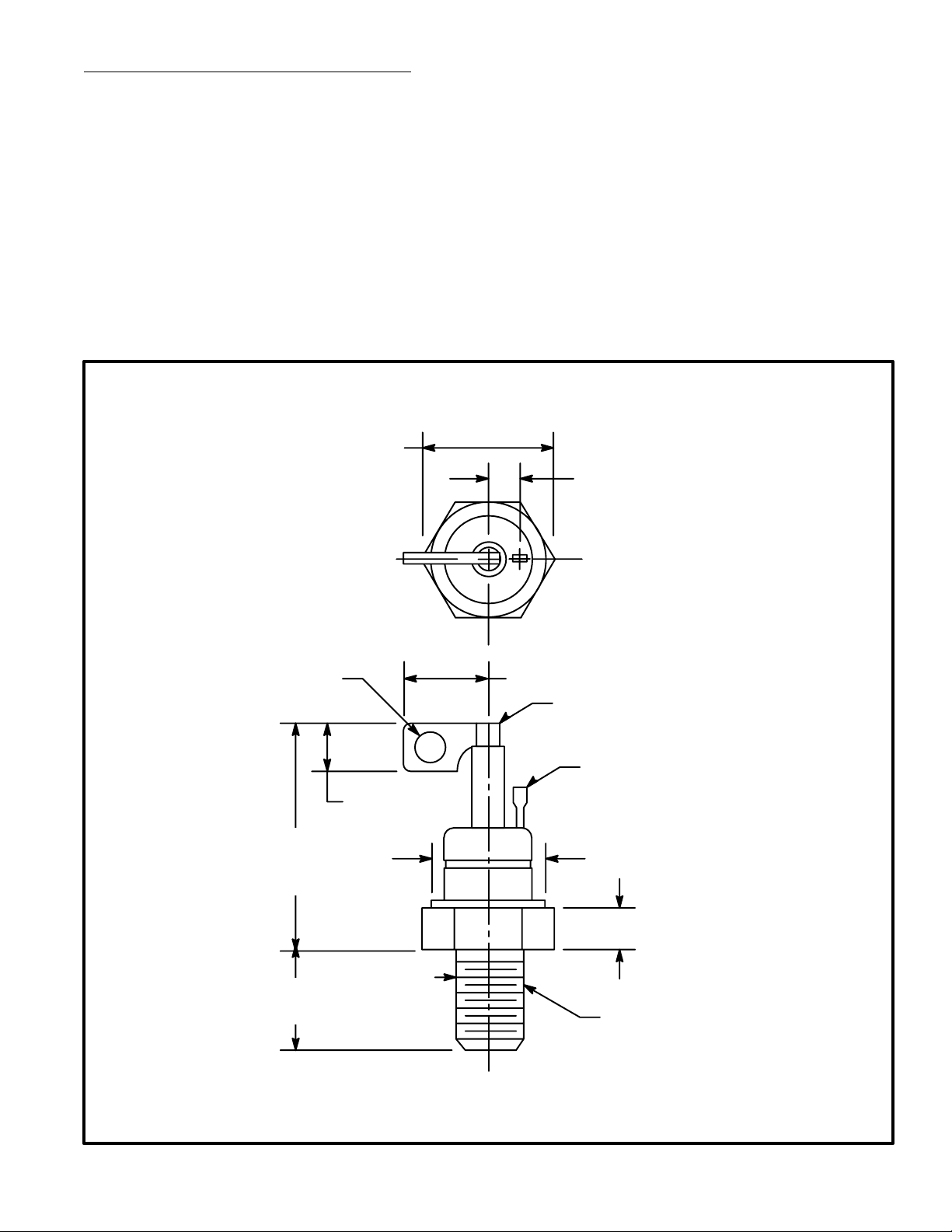
1.227 (31.18) Dia
(Across Corners)
.280 (7.11)
2.54V. . . . . . . . . . . . . . . . . . . . . . . . . . . . . . . . . . . . . . . . . . .
1.7V. . . . . . . . . . . . . . . . . . . . . . . . . . . . . . . . . . . . . . . . . . .
20mA. . . . . . . . . . . . . . . . . . . . . . . . . . . . . . . . . . .
20mA. . . . . . . . . . . . . . . . . . . . . . . . . . . . . . . . . . . .
3V. . . . . . . . . . . . . . . . . . . . . . . . . . . . . .
0.25V. . . . . . . . . . . . . . . . . . . . . . .
25µC. . . .
.260 (6.6) Dia Max
1.810
(45.97)
Max
.812
(20.6)
.650 (16.51) Max
Cathode
Gate
.415 (10.55)
1.031 (26.18) Dia Max
.500 (12.7) Max
Anode
1/2–20 UNF
(Terminal 3)
 Loading...