


NTE5351
Silicon Controlled Rectifier (SCR)
for High Speed Switching
Features:
D Fast Turn–Off Time
D High di/dt and dv/dt Capabilities
D Shorted–Emitter Gate–Cathode Construction
D Center Gate Construction
Non–Repetitive Peak Reverse Voltage (Gate Open, Note 1), V
Non–Repetitive Peak Off–State Voltage (Gate Open, Note 1), V
Repetitive Peak Reverse Voltage (Gate Open, Note 1), V
Repetitive Peak Off–State Voltage (Gate Open, Note 1), V
RMS On–State Current (TC = +60°C, 180° conduction angle), I
Average On–State Current (TC = +60°C, 180° conduction angle), I
Peak Surge (Non–Repetitive) On–State Current, I
TSM
(TC = +60°C, for one full cycle at applied voltage)
60Hz (Sinusoidal) 80A. . . . . . . . . . . . . . . . . . . . . . . . . . . . . . . . . . . . . . . . . . . . . . . . . . . . . . . . .
50Hz (Sinusoidal) 65A. . . . . . . . . . . . . . . . . . . . . . . . . . . . . . . . . . . . . . . . . . . . . . . . . . . . . . . . .
Rate of Change of On–State Current (VD = 600V, IGT = 50mA, t = 1 to 8.3ms), di/dt 200A/µs. . . . .
Fusing Current (TJ = –40° to +100°C, t = 1 to 8.3ms), I2t 25A. . . . . . . . . . . . . . . . . . . . . . . . . . . . . . . .
Peak Forward Gate Power Dissipation (10µs Max, Note 2), P
Peak Reverse Gate Power Dissipation (10µs Max, Note 2), P
Average Gate Power Dissipation (10µs Max, Note 2), P
Operating Case Temperature Range, T
Storage Temperature Range, T
stg
Thermal Resistance, Junction–to–Case, R
Thermal Resistance, Junction–to–Ambient, R
C
thJC
thJA
G(AV)
Lead Temperature (During Soldering, 1/32” from seating plane, 10sec max), T
RROM
DROM
RSOM
DSOM
T(RMS)
GM
RGM
T(AV)
–40° to +100°C. . . . . . . . . . . . . . . . . . . . . . . . . . . . . . . . . . . .
–40° to +150°C. . . . . . . . . . . . . . . . . . . . . . . . . . . . . . . . . . . . . . . . . .
8°C/W. . . . . . . . . . . . . . . . . . . . . . . . . . . . . . . . . . . . . . .
40°C/W. . . . . . . . . . . . . . . . . . . . . . . . . . . . . . . . . . . .
L
+225°C. . . . . . . . .
700V. . . . . . . . . . . . . . . . . . . . .
700V. . . . . . . . . . . . . . . . . . . .
600V. . . . . . . . . . . . . . . . . . . . . . . . . .
600V. . . . . . . . . . . . . . . . . . . . . . . . .
5.0A. . . . . . . . . . . . . . . . . . . .
3.2A. . . . . . . . . . . . . . . . . .
3W. . . . . . . . . . . . . . . . . . . . . . . . .
3W. . . . . . . . . . . . . . . . . . . . . . . .
0.5W. . . . . . . . . . . . . . . . . . . . . . . . . . . .
Note 1. These values do not apply if there is a positive gate signal. Gate must be negatively biased.
Note 2. An y pr oduct of g ate c urrent a nd g ate v oltage w hich results in a g ate p ower l ess than the m aximum
is permitted .
Electrical Characteristics: (At “Maximum Ratings” and TC = +25°C unless otherwise specified)
Parameter Symbol Test Conditions Min Typ Max Unit
Peak Off–State Forward Current I
Peak Off–State Reverse Current I
Instantaneous On–State Voltage v
Instantaneous Holding Current i
Critical Rate of Rise of Off–State
Current
DC Gate Trigger Current I
DC Gate Trigger Voltage V
Gate Controlled Turn–On Time t
Circuit Commutated Turn–Off
Time
dv/dt VD = 600V, exponential voltage rise,
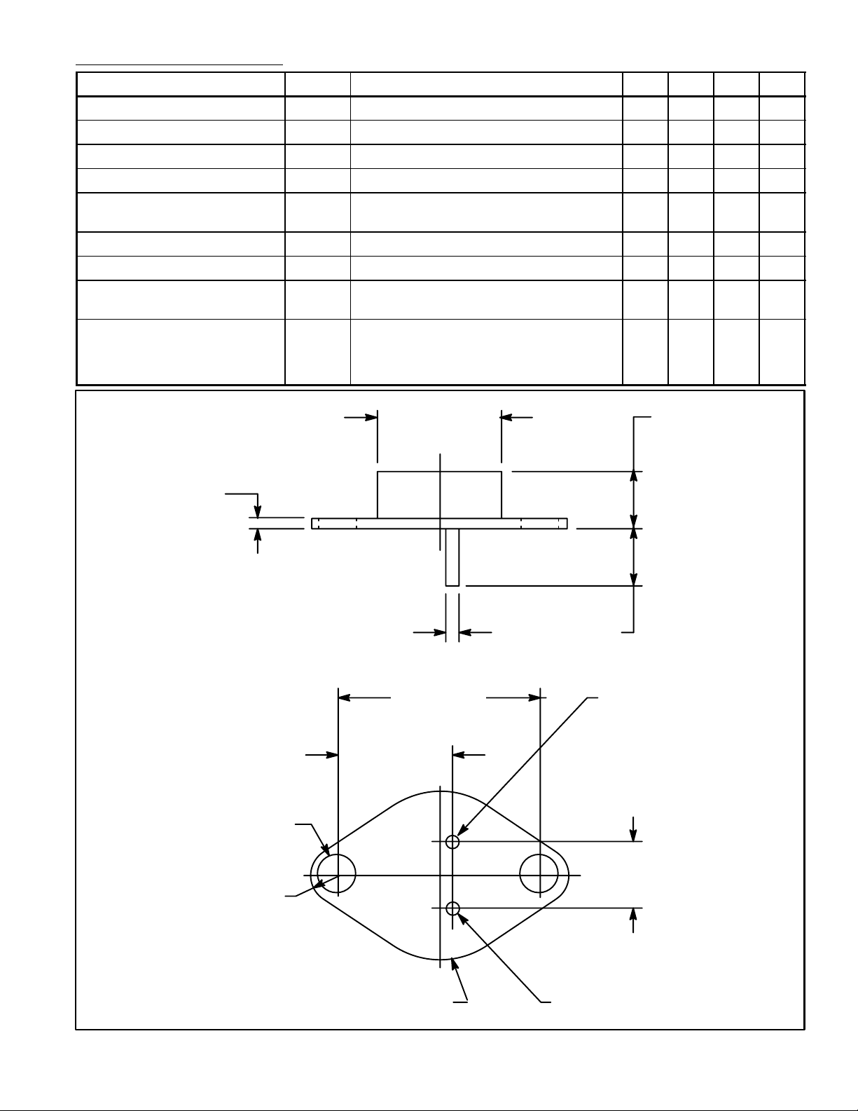
.062 (1.57)
DOM
ROM
T
HO
GT
GT
gt
t
q
VD = 600V, TC = +100°C, Gate Open – 0.5 3.0 mA
VD = 600V, TC = +100°C, Gate Open – 0.3 1.5 mA
iT = 30A Peak – 2.2 3.0 V
Gate Open – 20 50 mA
100 250 – V/µs
TC = +80°C, Gate Open
VD = 12V, RL = 30Ω – 15 40 mA
VD = 12V, RL = 30Ω – 1.8 3.5 V
VDX = 600V, IGT = 300mA, tr = 0.1µs,
IT = 2A peak
VCX = 600V, iT = 2A, pulse durat ion = 50µs,
dv/dt = 100V/µs, –di/dt = –10A/µs,
IGT = 100mA, VGT = 0V (at turn–off),
TC = +80°C
.485 (12.3)
– 0.7 – µs
– 4 6 µs
.295 (7.5)
Dia
.147 (3.75) Dia
(2 Places)
.145 (3.7) R Max
.031 (0.78) Dia
.960 (24.3) Gate
.580 (14.7)
.360
(9.14)
Min
.200
(5.08)
CathodeAnode/Case
 Loading...