TL/EE12584
NSAM266SA CompactSPEECH Digital Speech Processor with Serial Flash Interface
March 1996
NSAM266SA CompactSPEECHTMDigital Speech
Processor with Serial Flash Interface
General Description
The NSAM266SA is a member of National Semiconductor’s
CompactSPEECH Digital Speech Processor family. This
processor provides Digital Answering Machine (DAM) functionality to embedded systems.
The CompactSPEECH interfaces with National Semiconductor’s NM29A040 and NM29A080 Serial Flash memory
devices to provide a cost-effective solution for DAM and
Cordless DAM (CDAM) applications.
The CompactSPEECH processor integrates the functions of
a traditional Digital Signal Processing (DSP) chip and the
CR16A, a 16-bit general-purpose RISC core implementation
of the CompactRISC
TM
architecture. It contains system support functions such as Interrupt Control Units, Codec interface, MICROWIRE
TM
interfaces to a microcontroller and
Serial Flash, WATCHDOG
TM
timer, and a Clock Generator.
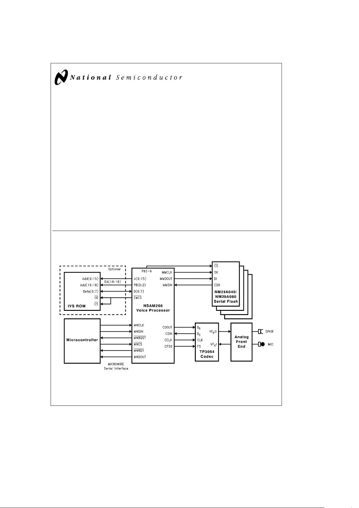
The CompactSPEECH processor operates as a slave peripheral that is controlled by an external microcontroller via
a serial MICROWIRE interface. In a typical DAM environment, the microcontroller controls the analog circuits, buttons and display, and activates the CompactSPEECH by
sending it commands. The CompactSPEECH processor executes the commands and returns status information to the
microcontroller.
The CompactSPEECH firmware implements voice compression and decompression, tone detection and generation,
message storage management, speech synthesis for timeand-day stamp, and supports user-defined voice prompts in
various languages.
The CompactSPEECH implements echo-cancellation techniques to support high-quality DTMF tone detection during
message playback.
The CompactSPEECH can synthesize messages in various
languages via the International Vocabulary Support (IVS)
mechanism. The NSAM266SA can store vocabularies on
either Serial Flash, or Expansion ROM memories. DAM
manufacturers can thus create machines that ‘‘speak’’ in
different languages, simply by using other vocabularies. For
more details about IVS, refer to the
IVS User’s Manual.
1.0 Hardware
1.1 BLOCK DIAGRAMS
NSAM266SA Basic Configuration
TL/EE/12584– 1
TRI-STATEÉis a registered trademark of National Semiconductor Corporation.
CompactSPEECH
TM
, CompactRISCTM, COPSTMMicrocontrollers, HPCTM, MICROWIRETM, MICROWIRE/PLUSTMand WATCHDOGTMare trademarks of National Semiconductor Corporation.
C
1996 National Semiconductor Corporation RRD-B30M46/Printed in U. S. A.
http://www.national.com

Features
Y
Designed around the CR16A, a 16-bit general-purpose
RISC core implementation of the CompactRISC architecture
Y
20.48 MHz operation
Y
On-chip DSP Module (DSPM) for high-speed DSP
operations
Y
On-chip codec clock generation and interface
Y
Power-down mode
Y
Selectable speech compression rate of 5.2 kbit/s or
7.3 kbit/s with silence compression
Y
Up to 16 minutes recording on a 4-Mbit Serial Flash
(more than 1 hour total recording time on four devices)
Y
The number of messages that can be stored is limited
only by memory size
Y
MICROWIRE slave interface to an external
microcontroller
Y
MICROWIRE master interface to Serial Flash memory
devices
Y
Storage and management of messages
Y
Programmable message tag for message categorization, e.g., Mailboxes, InComing Messages (ICM), OutGoing Messages (OGM)
Y
Skip forward or backward during message playback
Y
Digital volume control
Y
Variable speed playback
Y
Supports external vocabularies, using Serial Flash or
expansion ROM
Y
Multi-lingual speech synthesis using International Vocabulary Support (IVS)
Y
Vocabularies available in: English, Japanese, Mandarin,
German, French and Spanish
Y
DTMF generation and detection
Y
DTMF detection during OutGoing Message playback
Y
Single tone generation
Y
Telephone line functions, including busy and dial tone
detection
Y
Call screening (input signal echoed to codec output)
Y
Real-time clock
Y
Direct access to message memory
Y
Supports long-frame and short-frame codecs
Y
Supports up to four 4-Mbit, or two 8-Mbit, Serial Flash
devices
Y
Supports prerecorded IVS and OGM on Serial Flash
Y
Available in 68-pin PLCC and 100-pin PQFP packages
http://www.national.com 2

Table of Contents
1.0 HARDWARE
1.1 Block Diagrams
1.2 Pin Assignment
1.2.1 PinÐSignal Assignment
1.2.2 Pin Assignment in the 68-PLCC Package
1.2.3 Pin Assignment in the 100-PQFP Package
1.3 Functional Description
1.3.1 Resetting
1.3.2 Clocking
1.3.3 Power-down Mode
1.3.4 Power and Grounding
1.3.5 Memory Interface
1.3.6 Codec Interface
1.4 Specifications
1.4.1 Absolute Maximum Ratings
1.4.2 Electrical Characteristics
1.4.3 Switching Characteristics
1.4.4 Synchronous Timing Tables
1.4.5 Timing Diagrams
2.0 SOFTWARE
2.1 Overview
2.1.1 DSP-based Algorithms
2.1.2 System Support
2.1.3 Peripherals Support
2.2 CompactSPEECH CommandsÐQuick Reference
Table
2.3 The State Machine
2.4 Command Execution
2.5 Tunable Parameters
2.6 Messages
2.6.1 Message Tag
2.7 Speech Compression
2.8 Tone and No-Energy Detection
2.9 Speech Synthesis
2.9.1 Explanation of Terms
2.9.2 Vocabulary Design
2.9.3 IVS Vocabulary Components
2.9.4 The IVS Tool
2.9.5 How to Use the IVS Tool With the
CompactSPEECH
2.10 Initialization
2.11 Microwire Serial Interface
2.12 Signal Description
2.12.1 Signal Use in the Interface Protocol
2.12.2 Interface Protocol Error Handling
2.13 The Master Microwire Interface
2.13.1 Master MICROWIRE Data Transfer
2.14 Command Description
APPENDIX A
SCHEMATIC DIAGRAMS
http://www.national.com3

1.0 Hardware (Continued)
1.2 PIN ASSIGNMENT
The following sections detail the pins of the NSAM266SA
processor. Slashes separate the names of signals that
share the same pin.
1.2.1 PinÐSignal Assignment
Table 1-1 shows all the pins, and the signals that use them
in different configurations. It also shows the type and direction of each signal.
TABLE 1-1. CompactSPEECH PinÐSignal Assignment
Pin Name Type Signal Name I/O
A(0:15) TTL A(0:15) Output
CCLK TTL CCLK Output
CDIN TTL CDIN Input
CDOUT TTL CDOUT Output
CFS0 TTL CFS0 Output
D(0:7) TTL D(0:7) I/O
MWCS TTL (Note A) MWCS Input
TST TTL TST Input
MWRDY TTL MWRDY I/O
MWRQST TTL MWRQST I/O
MWDOUT TTL MWDOUT Output
PB(0:2) TTL EA(16:18) Output
(Note B)
PB(3:6) TTL CS(0:3) Output
(Note C)
EMCS/ TTL1 (Note D) EMCS Output
ENV0 CMOS (Note E) ENV0 Input
MWCLK TTL MWCLK Input
MWDIN TTL MWDIN Input
MMCLK TTL1 (Note D) MMCLK Output
MMDIN TTL MMDIN Input
MMDOUT TTL1 (Note D) MMDOUT Output
CFS0 CMOS CFS0 Output
RESET Schmitt (Note A) RESET Input
V
CC
Power V
CC
V
SS
Power V
SS
X1 XTAL X1 OSC
X2/CLKIN XTAL X2 OSC
TTL CLKIN Input
Note A: Schmitt trigger input.
Note B: Virtual address lines for IVS ROM.
Note C: Chip select lines for Serial Flash devices.
Note D: TTL1 output signals provide CMOS levels in the steady
state, for small loads.
Note E: Input during reset, CMOS level input.
http://www.national.com 4
1.0 Hardware (Continued)
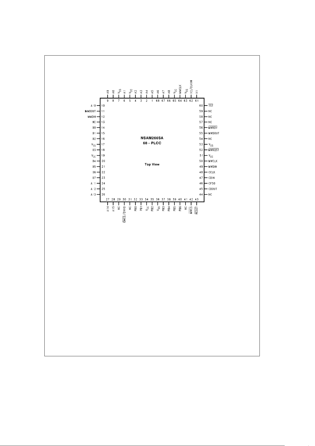
1.2.2 Pin Assignment in the 68-PLCC Package
TL/EE/12584– 3
Note: Pins marked NC should not be connected.
FIGURE 1-1. 68-PLCC Package Connection Diagram
http://www.national.com5
1.0 Hardware (Continued)
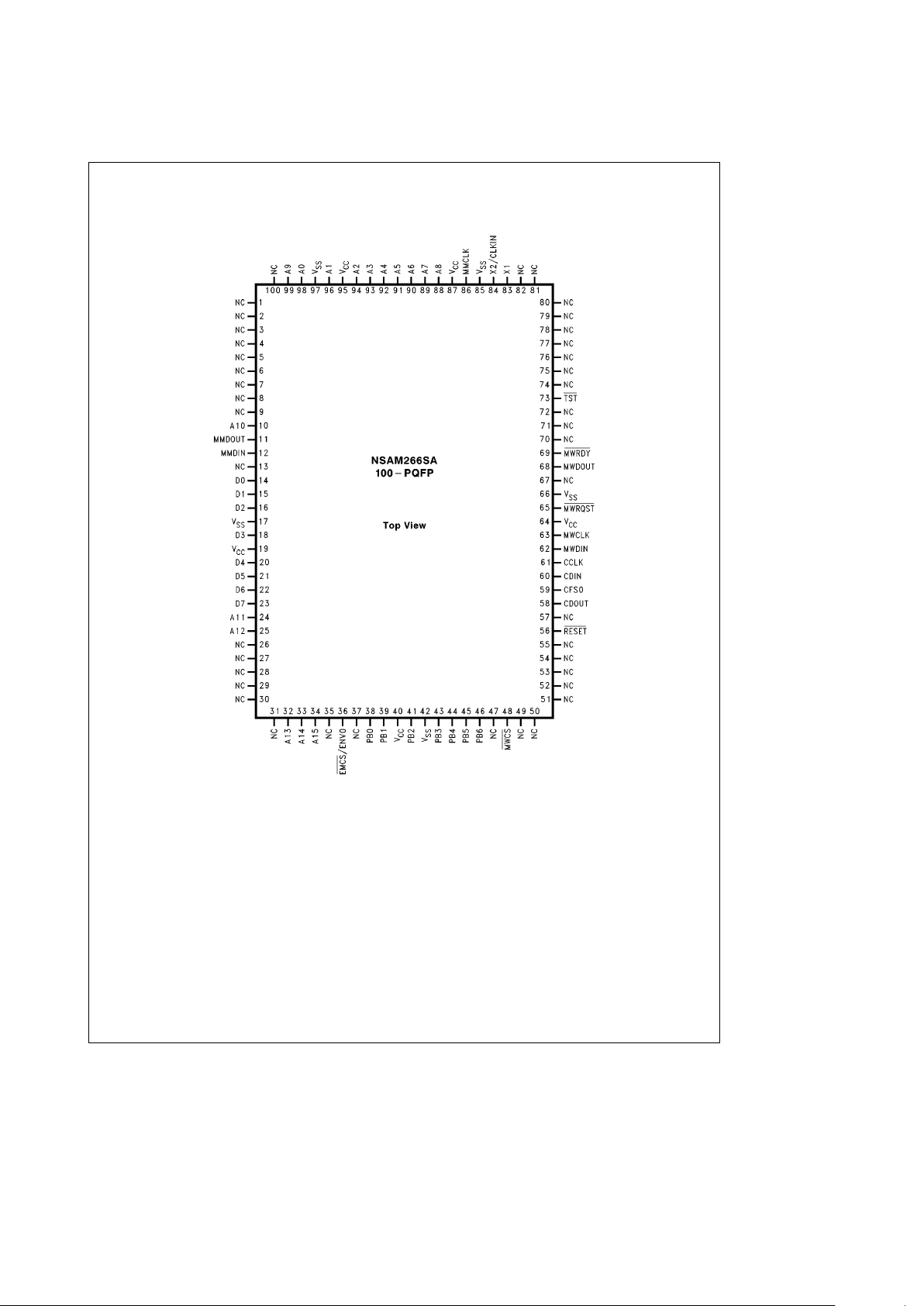
1.2.3 Pin Assignment in the 100-PQFP Package
TL/EE/12584– 4
Note: Pins marked NC should not be connected.
FIGURE 1-2. 100-PQFP Package Connection Diagram
http://www.national.com 6
1.0 Hardware (Continued)
1.3 FUNCTIONAL DESCRIPTION
This section provides details of the functional characteristics of the CompactSPEECH processor. It is divided into the
following sections:
Resetting
Clocking
Power-down Mode
Power and Grounding
Memory Interface
Codec Interface
1.3.1 Resetting
The RESET
pin is used to reset the CompactSPEECH proc-
essor.
On application of power, RESET
must be held low for at
least t
pwr
after VCCis stable. This ensures that all on-chip
voltages are completely stable before operation. Whenever
RESET
is applied, it must also remain active for not less
than t
RST
. During this period, and for 100 ms after, the TST
signal must be high. This can be done with a pull-up resistor
on the TST
pin.
The value of MWRDY is undefined during the reset period,
and for 100 ms after. The microcontroller should either wait
before polling the signal for the first time, or the signal
should be pulled high during this period.
Upon reset, the ENV0 signal is sampled to determine the
operating environment. During reset, the EMCS
/ENV0 pin is
used for the ENV0 input signals. An internal pull-up resistor
sets ENV0 to 1.
After reset, the same pin is used for EMCS
.
System Load on ENV0
For any load on the ENV0 pin, the voltage should not drop
below V
ENVh
.
If the load on the ENV0 pin causes the current to exceed
10 mA, use an external pull-up resistor to keep the pin at 1.
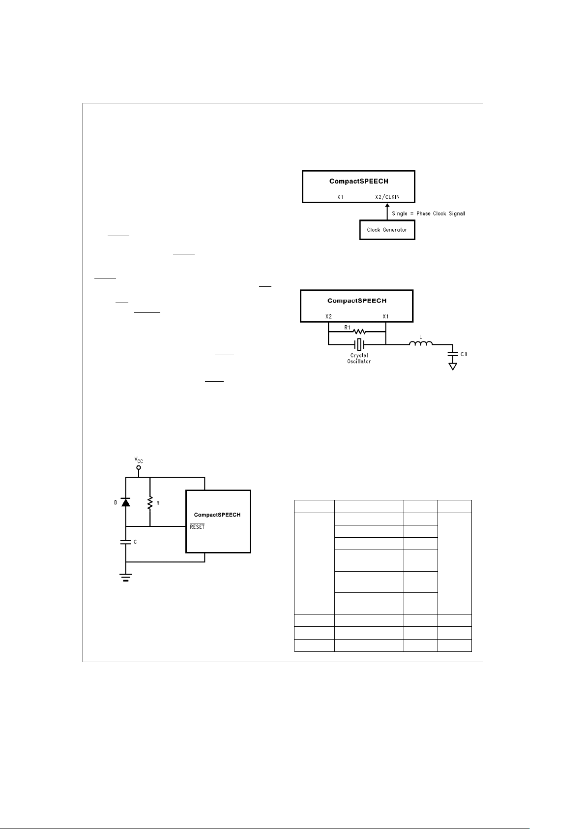
Figure 1-3
shows a recommended circuit for generating a
reset signal when the power is turned on.
TL/EE/12584– 5
FIGURE 1-3. Recommended Power-On Reset Circuit
1.3.2 Clocking
The CompactSPEECH provides an internal oscIllator that
interacts with an external clock source through the X1 and
X2/CLKIN pins. Either an external single-phase clock signal, or a crystal oscillator, may be used as the clock source.
External Single-Phase Clock Signal
If an external single-phase clock source is used, it should be
connected to the CLKIN signal as shown in
Figure 1-4
, and
should conform to the voltage-level requirements for CLKIN
stated in Section 1.4.2.
TL/EE/12584– 6
FIGURE 1-4. External Clock Source
Crystal Oscillator
A crystal oscillator is connected to the on-chip oscillator
circuit via the X1 and X2 signals, as shown in
Figure 1-5
.
TL/EE/12584– 7
FIGURE 1-5. Connections for an
External Crystal Oscillator
Keep stray capacitance and inductance, in the oscillator circuit, as low as possible. The crystal resonator, and the external components, should be as close to the X1 and
X2/CLKIN pins as possible, to keep the trace lengths in the
printed circuit to an absolute minimum.
You can use crystal resonators with maximum load capacitance of 20 pF, although the oscillation frequency may differ
from the crystal’s specified value.
Table 1-2 lists the components in the crystal oscillator circuit.
TABLE 1-2. Crystal Oscillator Component List
Component Parameters Values Tolerance
Resonator
Crystal
Resonance Frequency 40.96 MHz
N/A
Third Overtone Parallel
Type AT-Cut
Maximum Serial
50X
Resistance
Maximum Shunt
7pF
Capacitance
Maximum Load
12 pF
Capacitance
Resistor R1 10 MX 5%
Capacitor C1 1000 pF 20%
Inductor L 3.9 mH 10%
http://www.national.com7

1.0 Hardware (Continued)
1.3.3 Power-Down Mode
Power-down mode is useful during a power failure, when the
power source for the CompactSPEECH is a backup battery,
or in battery powered devices, while the CompactSPEECH
is idle.
In power-down mode, the clock frequency of the CompactSPEECH is reduced, and some of the processor modules
are deactivated. As a result, the CompactSPEECH consumes much less power than in normal-power mode
(
k
1.5 mA). Although the CompactSPEECH does not perform all its usual functions in power-down mode, it still
keeps stored messages and maintains the time of day.
Note: In power-down mode all the chip select signals, CS0 to CS3, are set
to 1. To guarantee that there is no current flow from these signals to
the Serial Flash devices, the power supply to these devices must not
be disconnected.
The CompactSPEECH stores messages, and all memory
management information, in flash memory. Thus, there is no
need to maintain the power to the processor to preserve
stored messages. If the microcontroller’s real-time clock
(and
not
the CompactSPEECH’s real-time clock) is used to
maintain the time and day, neither the flash nor the
CompactSPEECH require battery backup during power failure. In this case, when returning to normal mode, the microcontroller should perform the initialization sequence, as described in Section 2.10, and use the SETD command to set
the time and day.
To keep power consumption low in power-down mode, the
RESET
, MWCS, MWCLK and MWDIN signals should be
held above V
CC
b
0.5V or below V
SS
a
0.5V.
The PDM (Go To Power-down Mode) command switches
the CompactSPEECH to power-down mode. (For an explanation of the CompactSPEECH commands, see Section
2.14.) It may only be issued when the CompactSPEECH is
in the IDLE state. (For an explanation of the CompactSPEECH states, see Section 2.3.) If it is necessary to switch
to power-down mode from any other state, the controller
must first issue an S command to switch the CompactSPEECH to the IDLE state, and then issue the PDM command. Sending any command while in power-down mode
resets the CompactSPEECH detectors, and returns the
CompactSPEECH to normal operation mode.
1.3.4 Power and Grounding
The CompactSPEECH processor requires a single 5V power supply, applied to the V
CC
pins.
The grounding connections are made on the GND pins.
For optimal noise immunity, the power and ground pins
should be connected to V
CC
and the ground planes, respec-
tively, on the printed circuit board. If V
CC
and the ground
planes are not used, single conductors should be run directly from each V
CC
pin to a power point, and from each GND
pin to a ground point. Avoid daisy-chained connections.
Use decoupling capacitors to keep the noise level to a minimum. Attach standard 0.1 mF ceramic capacitors to the V
CC
and GND pins, as close as possible to the CompactSPEECH.
When you build a prototype, using wire-wrap or other methods, solder the capacitors directly to the power pins of the
CompactSPEECH socket, or as close as possible, with very
short leads.
1.3.5 Memory Interface
Serial Flash Interface
The CompactSPEECH supports up to four NM29A040
4-Mbit, or up to two NM29A080 8-Mbit, serial flash memory
devices for storing messages.
NM29A040
The NM29A040 is organized as 128 blocks of 128 pages,
each containing 32 bytes. A block is the smallest unit that
can be erased, and is 4 kbytes in size.
Not all 128 blocks are available for recording. Up to 10
blocks may contain bad bits, and one block is write-once
and holds the locations of these unusable blocks.
For further information about the NM29A040, see the
NM29A040 Datasheet.
NM29A080
The NM29A080 is organized as 256 blocks of 128 pages,
each containing 32 bytes. A block is the smallest unit that
can be erased, and is 4 kbytes in size.
Not all 256 blocks are available for recording. Up to 20
blocks may contain bad bits, and two blocks are write-once
and hold the locations of these unusable blocks.
For further information about the NM29A080, see the
NM29A080 Datasheet
.
Message Organization and Recording Time
A CompactSPEECH message uses at least one block. The
number of messages that can be stored on one NM29A040
device is 117 – 127, and on one NM29A080 device is 234 to
254 depending on the number of bad blocks. The maximum
recording time depends on four factors:
Ð The basic compression rate (5.2 kbit/s or 7.3 kbit/s)
Ð The amount of silence in the recorded speech
Ð The number of unusable blocks
Ð The number of recorded messages. (The basic memory
allocation unit for a message is a 4 kbyte block which
means that half a block in average is not used per recorded message)
Assuming a single message is recorded in all the available
memory space of a 4 Mbit device with all blocks usable, the
maximum recording time using 5.2 kbit/s compression is as
follows:
TABLE 1-3. Recording Time on 4 Mbit Device
Amount of Silence Total Record Time
0 13 min 9 sec
10 14 min 25 sec
15 15 min 7 sec
20 15 min 47 sec
25 16 min 25 sec
Serial Flash Endurance
The serial flash may be erased up to 100,000 times. To
reduce the effect of this limitation, the memory manager
utilizes the serial flash’s blocks evenly, i.e., each block is
erased more or less the same number of times, to ensure
that all blocks have the same lifetime.
http://www.national.com 8

1.0 Hardware (Continued)
Consider the following extensive usage of all the
NM29A040’s blocks:
1. Record 15 minutes of messages (until the memory is full).
2. Playback 15 minutes (all the recorded messages).
3. Delete all messages.
Assuming a NM29A040 device is used in this manner 24
times a day, its expected lifetime is:
Flash Lifetime
e
100,000/(24 * 365)e11.4 years
Thus the NM29A040 device will last for over ten years, even
when used for six hours of recording per day.
Note, that if an NM29A080 device is used, then, under the
same conditions, it will last for more than 20 years.
ROM Interface
IVS vocabularies can be stored in either serial flash and/or
ROM. The CompactSPEECH supports IVS ROM devices
through Expansion Memory. Up to 64 kbytes (64k x 8) of
Expansion Memory are supported directly. Nevertheless,
the CompactSPEECH uses bits of the on-chip port (PB) to
further extend the 64 kbytes address space up to
0.5 Mbytes address space.
ROM is connected to the CompactSPEECH using the data
bus, D(0:7), the address bus, A(0:15), the extended address
signals, EA(16:18), and Expansion Memory Chip Select,
EMCS
, controls. The number of extended address pins to
use may vary, depending on the size and configuration of
the ROM.
Reading from Expansion Memory
An Expansion Memory read bus-cycle starts at T1, when the
data bus is in TRI-STATE
É
, and the address is driven on the
address bus. EMCS
is asserted (cleared to 0) on a T2W1
cycle. This cycle is followed by three T2W cycles and one
T2 cycle. The CompactSPEECH samples data at the end of
the T2 cycle.
The transaction is terminated at T3, when EMCS
becomes
inactive (set to 1). The address remains valid until T3 is
complete. A T3H cycle is added after the T3 cycle. The
address remains valid until the end of T3H.
1.3.6 Codec Interface
The CompactSPEECH provides an on-chip interface to a
serial codec. This interface supports codec operation in
long- or short-frame formats. The format is selected with the
CFG command.
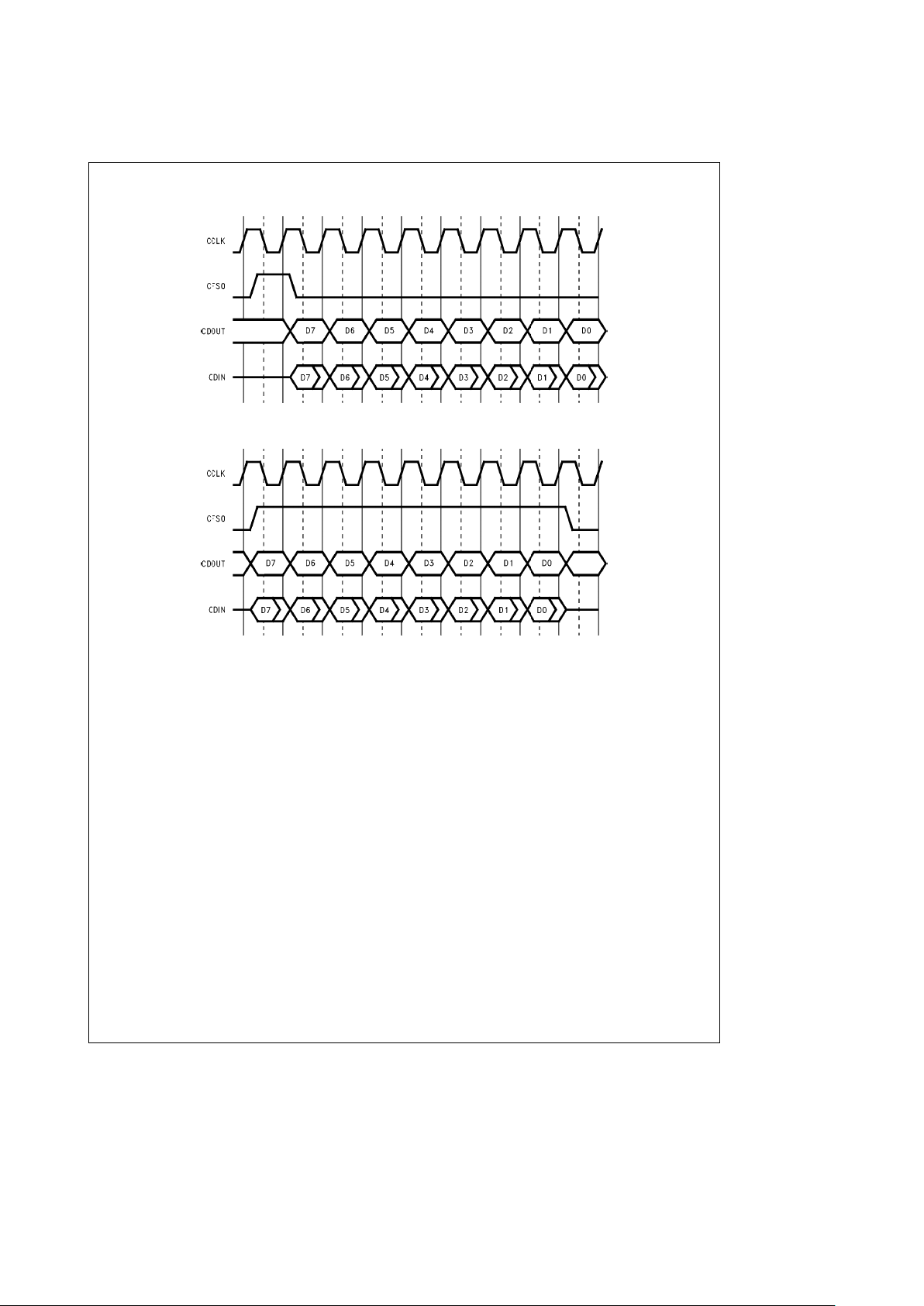
The codec interface uses four signalsÐCDIN, CDOUT,
CCLK and CFS0.
Data is transferred to the codec through the CDOUT pin.
Data is read from the codec through the CDIN pin.
Data transfer between the CompactSPEECH and the serial
codec starts by the CompactSPEECH asserting (setting to
1) the CFS0 frame synchronization signal. After one clock
cycle, the CompactSPEECH de-asserts (clears to 0) CFS0,
data from the CompactSPEECH is sent to the codec
through CDOUT, and simultaneously data from the codec is
sent to the CompactSPEECH through CDIN.
Short Frame Protocol
When short frame protocol is configured, eight data bits are
exchanged with each codec in each frame, i.e., CFS0 cycle.
Data transfer starts when CFS0 is set to 1 for one CCLK
cycle. The data is then transmitted, bit-by-bit, via the
CDOUT output pin. Concurrently, the received data is shifted in via the CDIN input pin. Data is shifted one bit in each
CCLK cycle.
Figure 1-6
shows how the codec interface signals behave
when short frame protocol is configured.
Long Frame Protocol
When long frame protocol is configured, eight data bits are
exhanged with each codec, as with the short frame protocol. However, for the long frame protocol, data transfer
starts by setting CFS0 to 1 for eight CCLK cycles. Simultaneously, the data for the first codec is shifted out bit-by-bit,
via the CDOUT output pin, as in short frame protocol. Concurrently, the received data is shifted in through the CDIN
input. The data is shifted one bit in each CCLK cycle.
Figure 1-7
shows how the codec interface signals behave
when long frame protocol is configured.
http://www.national.com9
1.0 Hardware (Continued)
TL/EE/12584– 8
FIGURE 1-6. Codec ProtocolÐShort Frame
TL/EE/12584– 9
FIGURE 1-7. Codec ProtocolÐLong Frame
http://www.national.com 10

1.0 Hardware (Continued)
1.4 SPECIFICATIONS
1.4.1 Absolute Maximum Ratings
If Military/Aerospace specified devices are required,
please contact the National Semiconductor Sales
Office/Distributors for availability and specifications.
Storage Temperature
b
65§Ctoa150§C
Temperature under Bias 0
§
Ctoa70§C
All Input or Output Voltages,
with Respect to GND
b
0.5V toa6.5V
Note: Absolute maximum ratings indicate limits beyond which permanent
damage may occur. Continuous operation at these limits is not intended; operation should be limited to those conditions specified below.
1.4.2 Electrical Characteristics T
A
e
0§Ctoa70§C, V
CC
e
5Vg10%, GNDe0V
Symbol Parameter Conditions Min Typ Max Units
V
IH
TTL Input,
2.0
V
CC
a
V
Logical 1 Input Voltage 0.5
V
IL
TTL Input, Logical 0 Input Voltage
b
0.5 0.8 V
V
XH
CLKIN Input, High Voltage External Clock 2.0 V
V
XL
CLKIN Input, Low Voltage External Clock 0.8 V
V
ENVh
ENV0 High Level, Input Voltage 3.6 V
V
Hh
CMOS Input with Hysteresis,
3.6 V
Logical 1 Input Voltage
V
HI
CMOS Input with Hysteresis,
1.1 V
Logical 0 Input Voltage
V
Hys
Hysteresis Loop Width (Note A) 0.5 V
V
OH
Logical 1 TTL, Output Voltage I
OH
eb
0.4 mA 2.4 V
V
OHWC
MMCLK, MMDOUT and EMCS I
OH
eb
0.4 mA 2.4 V
Logical 1, Output Voltage
I
OH
eb
50 mA (Note B) V
CC
b
0.2 V
V
OL
Logical 0, TTL Output Voltage I
OL
e
4 mA 0.45 V
I
OL
e
50 mA (Note B) 0.2 V
V
OLWC
MMCLK, MMDOUT and EMCS I
OL
e
4.0 mA 0.45 V
Logical 0, Output Voltage
I
OL
e
50 mA (Note B) 0.2 V
I
L
Input Load Current (Note C) 0VsV
IN
s
V
CC
b
5.0 5.0 mA
IO(Off) Output Leakage Current 0VsV
OUT
s
V
CC
b
5.0 5.0 mA
(I/O Pins in Input Mode) (Note C)
I
CC1
Active Supply Current Normal Operation Mode,
65 80 mA
Running Speech Applications (Note D)
I
CC2
Standby Supply Current Normal Operation Mode,
40 mA
DSPM Idle (Note D)
I
CC3
Power-Down Mode Power-Down Mode
1.5 mA
Supply Current (Notes D and E)
C
X
X1 and X2 Capacitance (Note A) 17 pF
Note A: Guaranteed by design.
Note B: Measured in power-down mode. The total current driven, or sourced, by all the CompactSPEECH’s output signals is
k
50 mA.
Note C: Maximum 20 mA for all pins together.
Note D: I
OUT
e
0, T
A
e
25§C, V
CC
e
5V, operating from a 40.96 MHz crystal, and running from internal memory with Expansion Memory disabled.
Note E: All input signals are tied to 1 or 0 (above V
CC
b
0.5 or below V
SS
a
0.5V).
http://www.national.com11
1.0 Hardware (Continued)
1.4.3 Switching Characteristics
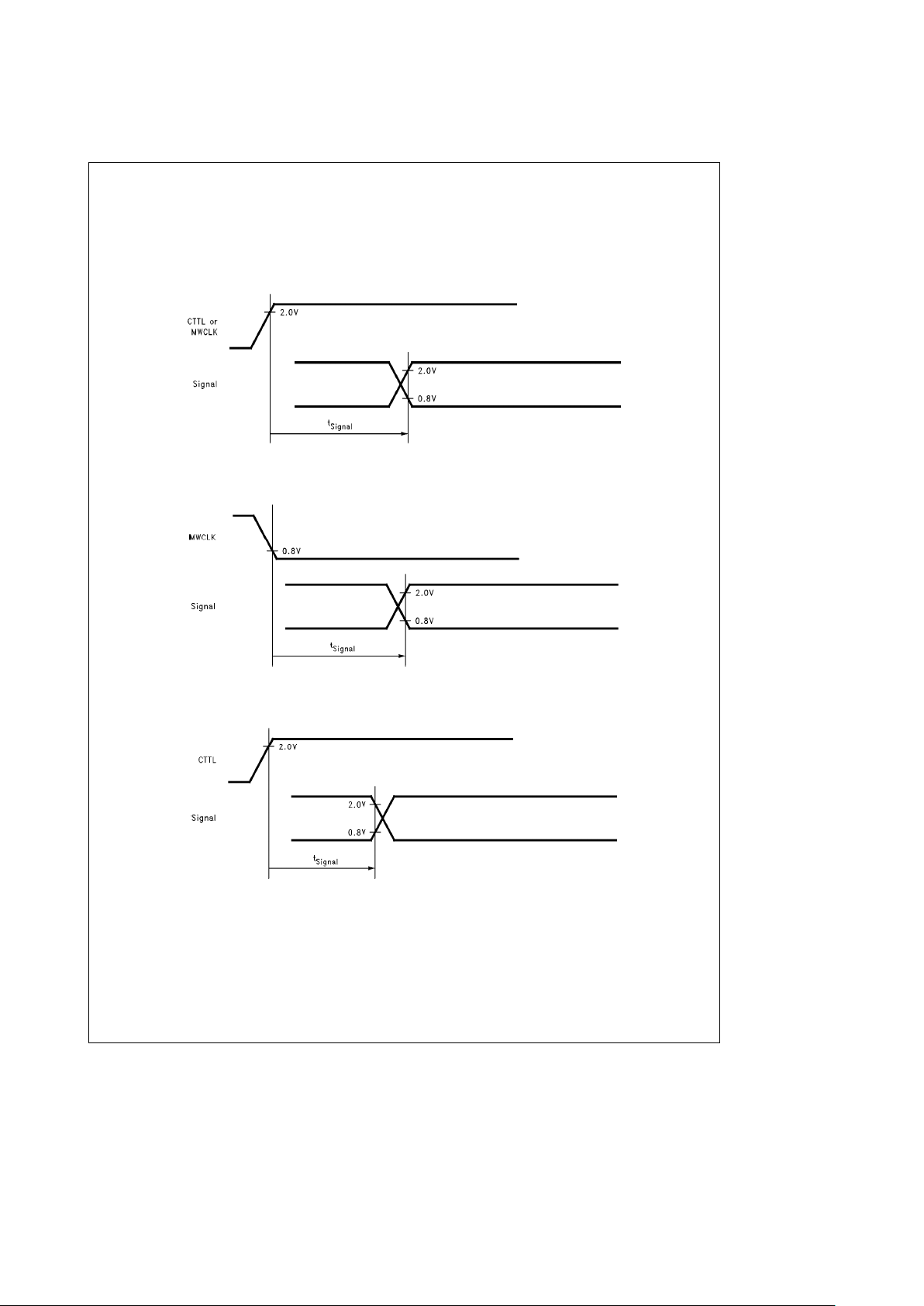
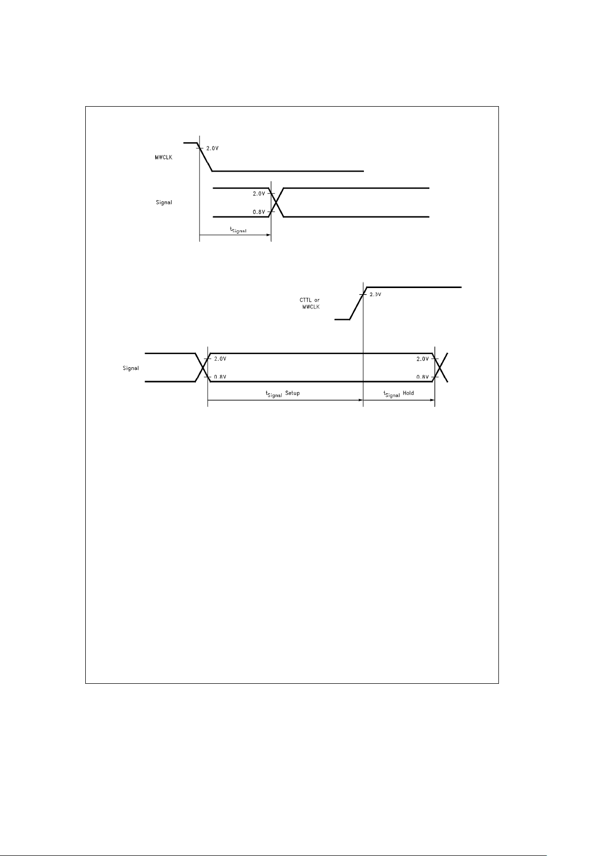
Definitions
All timing specifications in this section refer to 0.8V or 2.0V
on the rising or falling edges of the signals, as illustrated in
Figures 1-8
through
1-14,
unless specifically stated other-
wise.
Maximum times assume capacitive loading of 50 pF.
CLKIN crystal frequency is 40.96 MHz.
Note: CTTL is an internal signal and is used as a reference to explain the
timing of other signals. See
Figure 1-22
.
TL/EE/12584– 10
Signal valid, active or inactive time, after a rising edge of CTTL or MWCLK.
FIGURE 1-8. Synchronous Output Signals (Valid, Active and Inactive)
TL/EE/12584– 11
Signal valid time, after a falling edge of MWCLK.
FIGURE 1-9. Synchronous Output Signals (Valid)
TL/EE/12584– 12
Signal hold time, after a rising edge of CTTL.
FIGURE 1-10. Synchronous Output Signals (Hold)
http://www.national.com 12
1.0 Hardware (Continued)
TL/EE/12584– 13
Signal hold time, after a falling edge of MWCLK.
FIGURE 1-11. Synchronous Output Signals (Hold)
TL/EE/12584– 14
Signal setup time, before a rising edge of CTTL or MWCLK, and signal hold time after a rising edge of CTTL or MWCLK.
FIGURE 1-12. Synchronous Input Signals
http://www.national.com13
1.0 Hardware (Continued)
TL/EE/12584– 15
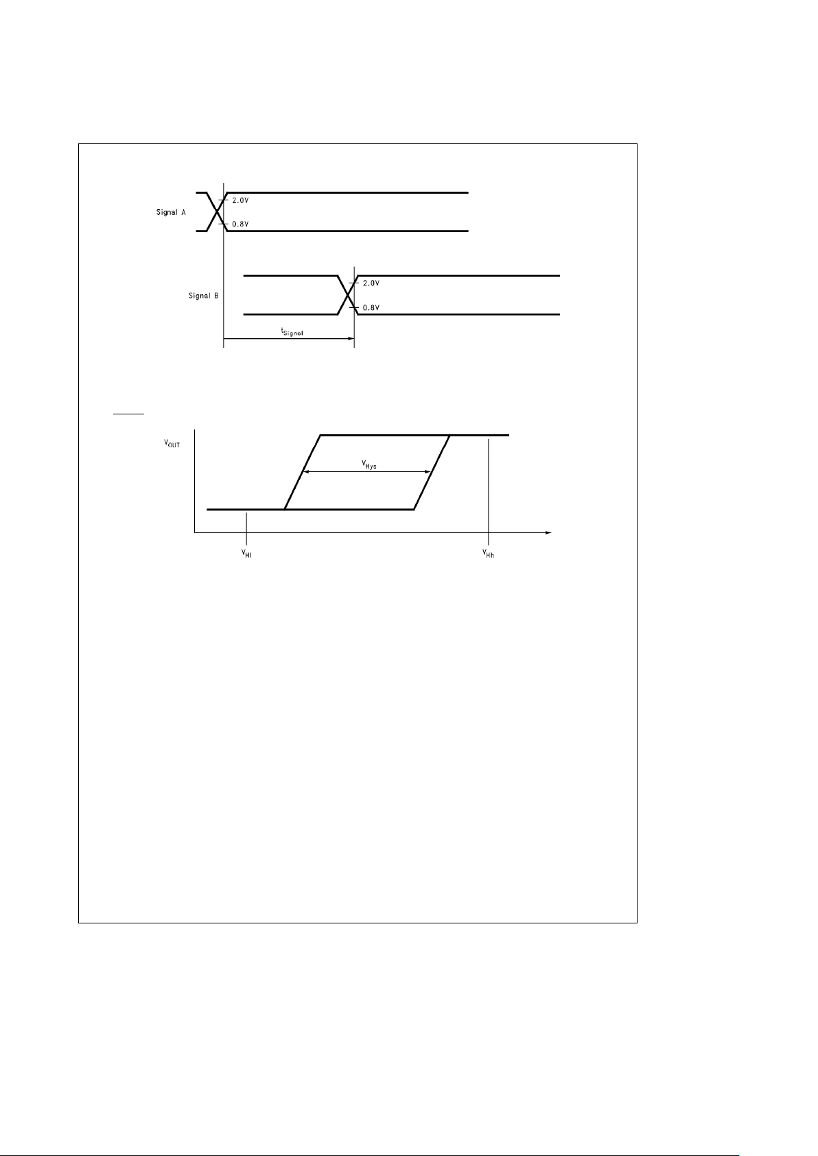
Signal B starts after rising or falling edge of signal A.
FIGURE 1-13. Asynchronous Signals
The RESET
signal has a Schmitt trigger input buffer.
Figure 1-14
shows the characteristics of the input buffer.
TL/EE/12584– 16
FIGURE 1-14. Hysteresis Input Characteristics
http://www.national.com 14

1.0 Hardware (Continued)
1.4.4 Synchronous Timing Tables
In this section, R.E. means Rising Edge and F.E. means Falling Edge.
OUTPUT SIGNALS
Symbol Figure Description Reference Conditions Min (ns) Max (ns)
t
Ah
1-17 Address Hold After R.E. CTTL 0.0
t
Av
1-17 Address Valid After R.E. CTTL, T1 12.0
t
CCLKa
1-15 CCLK Active After R.E. CTTL 12.0
t
CCLKh
1-15 CCLK Hold After R.E. CTTL 0.0
t
CCLKia
1-15 CCLK Inactive After R.E. CTTL 12.0
t
CDOh
1-15 CDOUT Hold After R.E. CTTL 0.0
t
CDOv
1-15 CDOUT Valid After R.E. CTTL 12.0
t
CTp
1-22 CTTL Clock Period (Note A) R.E. CTTL to next R.E. CTTL 48.8 50,000
t
EMCSa
1-17 EMCS Active After R.E. CTTL, T2W1 12.0
t
EMCSh
1-17 EMCS Hold After R.E. CTTL 0.0
t
EMCSia
1-17 EMCS Inactive After R.E. CTTL, T3 12.0
t
FSa
1-15 CFS0 Active After R.E. CTTL 25.0
t
FSh
1-15 CFS0 Hold After R.E. CTTL 0.0
t
FSia
1-15 CFS0 Inactive After R.E. CTTL 25.0
t
MMCLKa
1-20 Master MICROWIRE Clock Active After R.E. CTTL 12.0
t
MMCLKh
1-20 Master MICROWIRE Clock Hold After R.E. CTTL 0.0
t
MMCLKia
1-20 Master MICROWIRE Clock Inactive After R.E. CTTL 12.0
t
MMDOh
1-20 Master MICROWIRE Data Out Hold After R.E. CTTL 0.0
t
MMDOv
1-20 Master MICROWIRE Data Out Valid After R.E. CTTL 12.0
t
MWDOf
1-18 MICROWIRE Data Float (Note B) After R.E. MWCS 70.0
t
MWDOh
1-18 MICROWIRE Data Out Hold (Note B) After F.E. MWCK 0.0
t
MWDOnf
1-18 MICROWIRE Data No Float (Note B) After F.E. MWCS 0.0 70.0
t
MWDOv
1-18 MICROWIRE Data Out Valid (Note B) After F.E. MWCK 70.0
t
MWITOp
1-19 MWDIN to MWDOUT Propagation Time 70.0
t
MWRDYa
1-18 MWRDY Active After R.E. of CTTL 0.0 35.0
t
MWRDYia
1-18 MWRDY Inactive After F.E. MWCLK 0.0 70.0
t
PABCh
1-21 PB and MWRQST After R.E. CTTL 0.0
t
PABCv
1-21 PB and MWRQST After R.E. CTTL, T2W1 12.0
Note A: In normal operation mode t
CTp
must be 48.8 ns; in power-down mode, t
CTp
must be 50,000 ns.
Note B: Guaranteed by design, but not fully tested.
http://www.national.com15

1.0 Hardware (Continued)
INPUT SIGNALS
Symbol Figure Description Reference Conditions Min (ns)
t
CDIh
1-15 CDIN Hold After R.E. CTTL 0.0
t
CDIs
1-15 CDIN Setup Before R.E. CTTL 11.0
t
DIh
1-17 Data in Hold (D0:7) After R.E. CTTL T1, T3 or TI 0.0
t
DIs
1-17 Data in Setup (D0:7) Before R.E. CTTL T1, T3 or TI 15.0
t
MMDINh
1-20 Master MICROWIRE Data In Hold After R.E. CTTL 0.0
t
MMDINs
1-20 Master MICROWIRE Data In Setup Before R.E. CTTL 11.0
t
MWCKh
1-18 MICROWIRE Clock High (Slave) At 2.0V (Both Edges) 100.0
t
MWCKI
1-18 MICROWIRE Clock Low (Slave) At 0.8V (Both Edges) 100.0
t
MWCKp
1-18 MICROWIRE Clock Period (Slave) (Note A) R.E. MWCLK to next R.E. MWCLK 2.5 ms
t
MWCLKh
1-18 MWCLK Hold After MWCS becomes Inactive 50.0
t
MWCLKs
1-18 MWCLK Setup Before MWCS becomes Active 100.0
t
MWCSh
1-18 MWCS Hold After F.E. MWCLK 50.0
t
MWCSs
1-18 MWCS Setup Before R.E. MWCLK 100.0
t
MWDIh
1-18 MWDIN Hold After R.E. MWCLK 50.0
t
MWDIs
1-18 MWDIN Setup Before R.E. MWCLK 100.0
t
PWR
1-24 Power Stable to RESET R.E. (Note B) After VCCreaches 4.5V 30.0 ms
t
RSTw
1-23 RESET Pulse Width At 0.8V (Both Edges) 10.0 ms
t
Xh
1-22 CLKIN High At 2.0V (Both Edges) t
X1p
/2b5
t
XI
1-22 CLKIN Low At 0.8V (Both Edges) t
X1p
/2b5
t
Xp
1-22 CLKIN Clock Period R.E. CLKIN to next R.E. CLKIN 24.4
Note A: Guaranteed by design, but not fully tested in power-down mode.
Note B: Guaranteed by design, but not fully tested.
http://www.national.com 16
 Loading...