NSC LP2975IMMX-5.0, LP2975IMMX-12, LP2975IMM-5.0, LP2975IMM-12, LP2975AIMMX-3.3 Datasheet
...
LP2975
MOSFET LDO Driver/Controller
LP2975 MOSFET LDO Driver/Controller
September 1997
General Description
A high-current LDO regulator is simple to design with the
LP2975 LDO Controller. Using an external P-FET, the
LP2975 will deliver an ultra low dropout regulator with extremely low quiescent current.
High open loop gain assures excellent regulation and ripple
rejection performance.
The trimmed internal bandgap reference provides precise
output voltage over the entire operating temperature range.
Dropout voltage is “user selectable” by sizing the external
FET: the minimum input-output voltage required for operation is the maximum load current multiplied by the R
of the FET.
Overcurrent protection of the external FET is easily implemented by placing a sense resistor in series with V
57 mV detectionthresholdof the current sense circuitry minimizes dropout voltage and power dissipation in the resistor.
The standard product versions available provide output voltages of 12V, 5V, or 3.3V with guaranteed 25˚C accuracy of
1.5%(“A” grade) and 2.5%(standard grade).
DS
IN
Features
n Simple to use, few external components
n Ultra-small mini SO-8 package
n 1.5%(A grade) precision output voltage
n Low-power shutdown input
<
n
1 µA in shutdown
n Low operating current (180 µA typical
n Wide supply voltage range (1.8V to 24V)
n Built-in current limit amplifier
n Overtemperature protection
n 12V, 5V, and 3.3V standard output voltages
(ON)
n Can be programmed using external divider
n −40˚C to +125˚C junction temperature range
. The
Applications
n High-current 5V to 3.3V regulator
n Post regulator for switching converter
n Current-limited switch
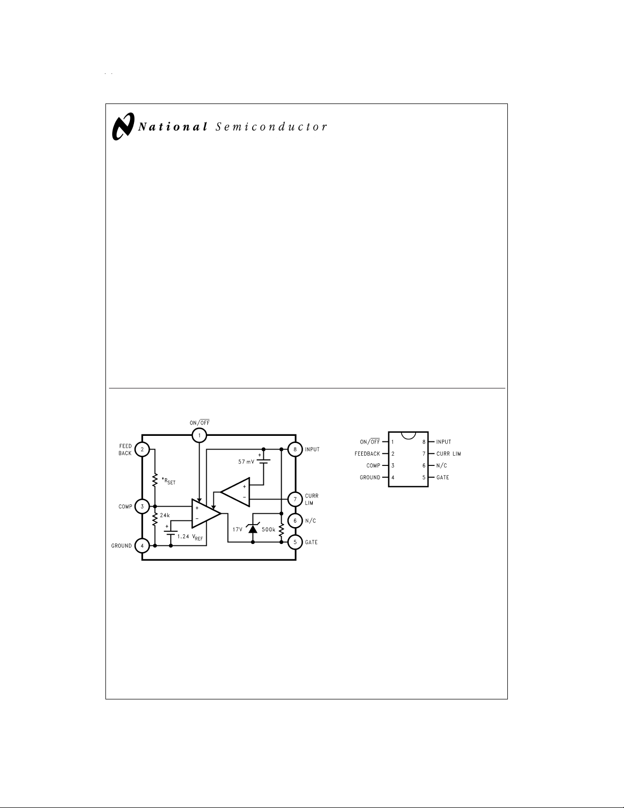
Block Diagram Connection Diagram
Surface Mount Mini SO-8 Package
Top View
For Order Numbers
See
Table 1
See NS Package Number MUA08A
of this Document
@
VIN= 5V)
DS100034-2
*R
values are: 208k for 12V part, 72.8k for 5V part, and 39.9k for 3.3V
SET
part.
© 1999 National Semiconductor Corporation DS100034 www.national.com
DS100034-1
Ordering Information
TABLE 1. Package Marking and Ordering Information
Output Voltage Grade Order Information Package Marking Supplied As:
12 A LP2975AIMMX-12 L47A 3.5k Units on Tape and Reel
12 A LP2975AIMM-12 L47A 250 Units on Tape and Reel
12 STD LP2975IMMX-12 L47B 3.5k Units on Tape and Reel
12 STD LP2975IMM-12 L47B 250 Units on Tape and Reel
5.0 A LP2975AIMMX-5.0 L46A 3.5k Units on Tape and Reel
5.0 A LP2975AIMM-5.0 L46A 250 Units on Tape and Reel
5.0 STD LP2975IMMX-5.0 L46B 3.5k Units on Tape and Reel
5.0 STD LP2975IMM-5.0 L46B 250 Units on Tape and Reel
3.3 A LP2975AIMMX-3.3 L45A 3.5k Units on Tape and Reel
3.3 A LP2975AIMM-3.3 L45A 250 Units on Tape and Reel
3.3 STD LP2975IMMX-3.3 L45B 3.5k Units on Tape and Reel
3.3 STD LP2975IMM-3.3 L45B 250 Units on Tape and Reel
www.national.com 2
Absolute Maximum Ratings (Note 1)
If Military/Aerospace specified devices are required,
please contact the National Semiconductor Sales Office/
Distributors for availability and specifications.
Storage Temperature Range −65˚C to +150˚C
Operating Junction Temperature
Range −40˚C to +125˚C
Lead Temp. (Soldering, 5 seconds) 260˚C
Input Supply Voltage (Survival) −0.3V to +26V
Input Supply Voltage (Operating) +1.8V to +24V
Current Limit Pins (Survival) −0.3V to +V
Comp Pin (Survival) −0.3V to +2V
Gate Pin (Survival) −0.3V to +V
ON/OFF Pin (Survival) −0.3V to +20V
Feedback Pin (Survival) −0.3V to +24V
ESD Rating 2 kV
Power Dissipation
(Note 2) Internally Limited
Electrical Characteristics
Limits in standard typeface are for TJ= 25˚C, and limits in boldface type apply over the full operating temperature range. Unless otherwise specified; V
Symbol Parameter Conditions Typ
V
REG
Regulation Voltage
(12V Versions)
Regulation Voltage
(5V Versions)
Regulation Voltage
(3.3V Versions)
V
COMP
I
Q
V
CL
V
ON/OFF
I
ON/OFF
I
G
Comp Pin Voltage V
Quiescent Current VIN= 5V 180 240 240
Current Limit
Sense Voltage
ON/OFF Threshold Output = ON
ON/OFF
Input Bias Current
Gate Drive Current (Sourcing) VG= 7.5V
Gate Drive Current (Sinking) V
V
R(V
G(MIN)
IN
Gate Clamp Voltage VIN= 24V
-G) Resistance from
Gate to V
IN
Open Loop
Voltage Gain
= 1.5V, VIN= 15V.
ON/OFF
LM2975AI-X.X
(Note 3)
LM2975I-X.X
(Note 3)
Min Max Min Max
IN
- 0.5V)>V
IN
(VIN- 5V)
<
<
V
IN
- 0.5V)>V
IN
(VIN- 4.5V)
<
<
V
IN
- 0.5V)>V
IN
(VIN- 3.3V)
<
V
IN
<
24V 12.0 11.820 12.180 11.700 12.300
GATE
11.640 12.360 11.520 12.480
24V 5.0 4.925 5.075 4.875 5.125
GATE
4.850 5.150 4.800 5.200
24V 3.3 3.250 3.350 3.217 3.383
GATE
<
24V 1.240 1.215 1.265 1.203 1.277
3.201 3.399 3.168 3.432
12.5<V
(V
>
5.5
(V
>
3.8
(V
>
REG
1.209 1.271 1.196 1.284
V
= 0V 0.01 11
ON/OFF
VIN= 15V
=0.9XV
V
FB
Output = OFF
V
= 1.5V
ON/OFF
REG
57 45 69 45 69
39 72 39 72
0.94
0.87
1.10 1.10
1.20 1.20
34
0.70 0.70
0.40 0.40
50 50 µA
75 75
3.5 1.3 1.3
=1.1XV
V
V
FB
G
FB
= 7.5V
=0.9XV
REG
REG
0.3 0.3
1100 350 350
40 40
17 15 19 15 19 V
=0.9XV
V
FB
VIN= 24V
V
ON/OFF
VIN= 15V
0.5V ≤ V
=0
GATE
REG
500 kΩ
5000 V/V
≤ 13
IN
IN
Units
V
V
µA320 320
mV
V
mA
µA
Note 1: Absolute maximum ratings indicate limits beyond which damage to the component may occur. Electrical specifications do not apply when operating the device outside of its rated operating conditions.
Note 2: The LP2975 has internal thermal shutdown which activates at a die temperature of about 150˚C. It should be noted that the power dissipated within the
LP2975 is low enough that this protection circuit should never activate due to self-heating, even at elevated ambient temperatures.
www.national.com3
Electrical Characteristics (Continued)
Note 3: Limits are 100%production tested at 25˚C. Limits over the operating temperature range are guaranteed through correlation using Statistical Quality Control
(SQC) methods. The limits are used to calculate National’s Average Outgoing Quality Level (AOQL).
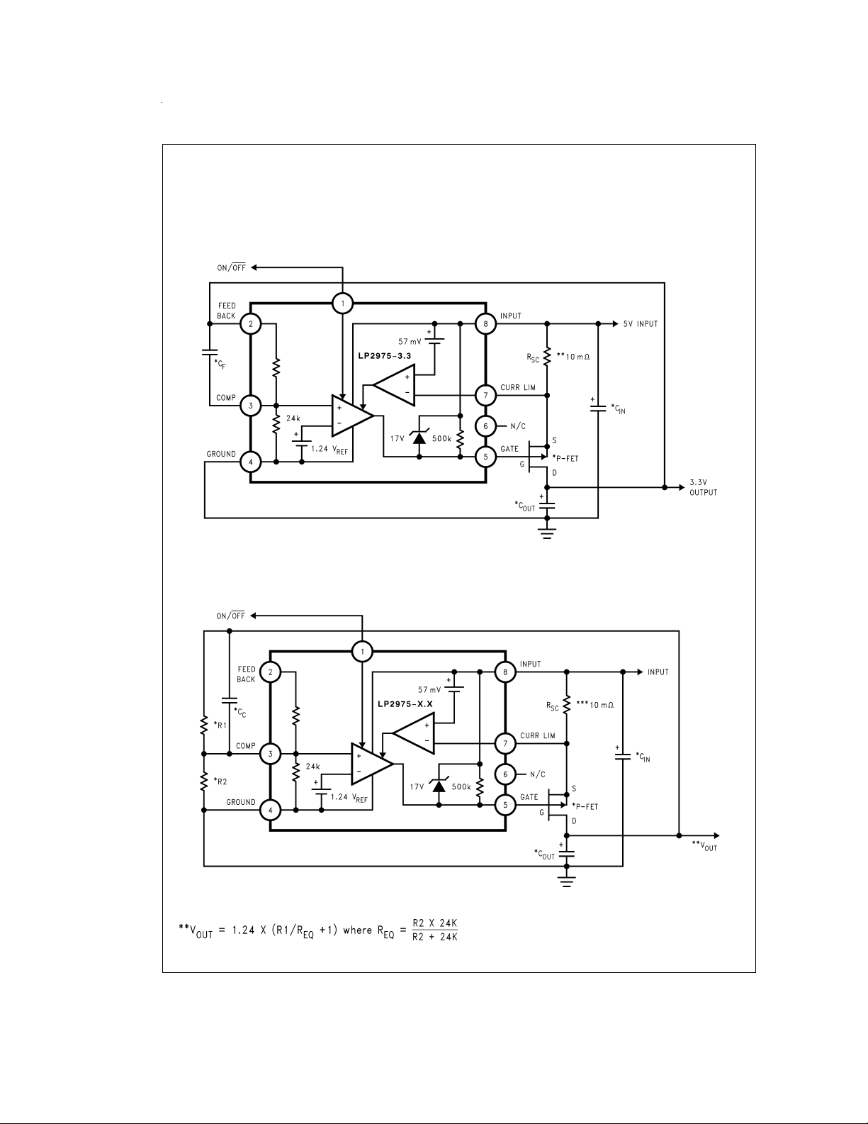
Typical Application Circuits
5V - 3.3V@5A LDO Regulator
*See Application Hints.
**If current limiting is not required, short out this resistor.
*See Application Hints.
***If current limiting is not required, short out this resistor.
DS100034-3
Adjustable Voltage 5A LDO Regulator
DS100034-4
www.national.com 4
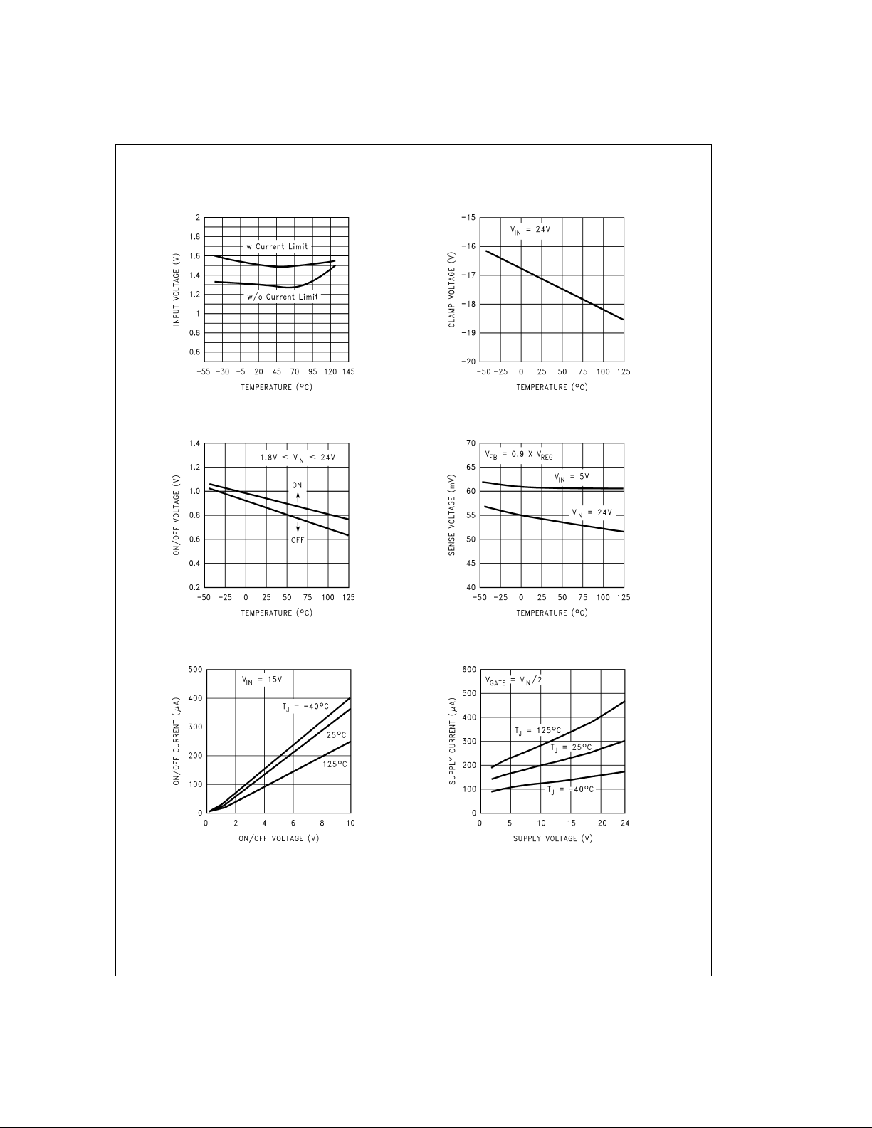
Typical Performance Characteristics Unless otherwise specified: T
is tied to 1.5V.
= 25˚C, CIN= 1 µF, ON/OFF pin
A
Minimum Operating Voltage
ON/OFF Threshold
DS100034-5
VINReferred Gate Clamp Voltage
DS100034-6
Current Limit Sense Voltage
ON/OFF Pin Current
DS100034-7
DS100034-9
DS100034-8
Supply Current
DS100034-10
www.national.com5
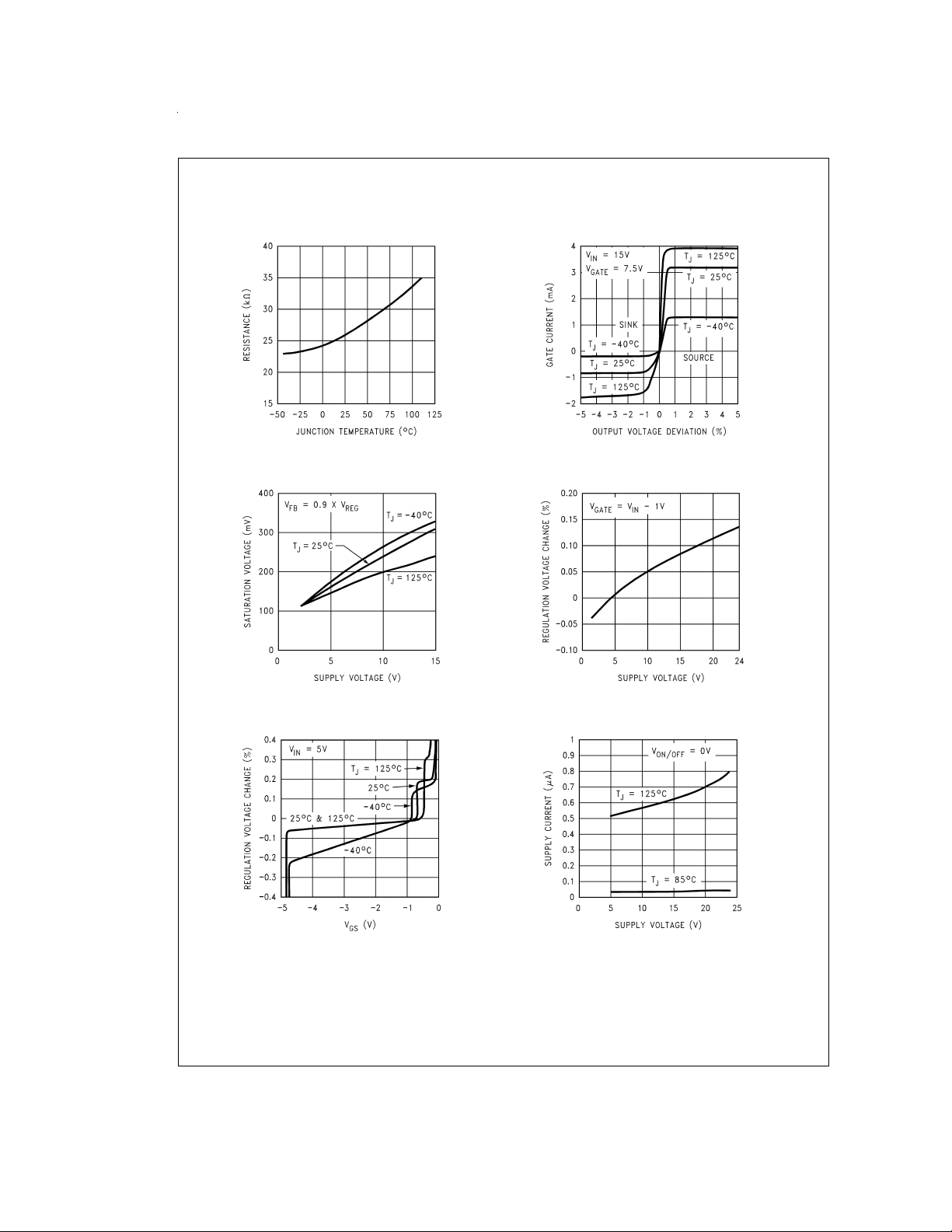
Typical Performance Characteristics Unless otherwise specified: T
is tied to 1.5V. (Continued)
= 25˚C, CIN= 1 µF, ON/OFF pin
A
ON/OFF Input Resistance
Gate-Ground Saturation
DS100034-11
Gate Current
DS100034-34
Line Regulation
DS100034-13
Load Regulation
DS100034-15
www.national.com 6
DS100034-14
Leakage Current
DS100034-35
 Loading...