NSC LP2960IN-3.3, LP2960IMX-5.0, LP2960IMX-3.3, LP2960IM-5.0, LP2960IM-3.3 Datasheet
...
LP2960
Adjustable Micropower 0.5A Low-Dropout Regulators
General Description
The LP2960 is a micropower voltage regulator with very low
dropout voltage (12 mV typical at 1 mA load and 470 mV
typical at 500 mA load) and very low quiescent current
(450 µA typical at 1 mA load).
The LP2960 is ideally suited for battery-powered systems:
the quiescent current increases only slightly at dropout,
which prolongs battery life.
The LP2960 retains all the desirable characteristics of the
LP2953, and offers increased output current.
The error flag goes low anytimetheoutput drops more than
5%out of regulation.
Reverse battery protection is provided.
The LP2960 requires only 10 µF of output capacitance for
stability (5V version).
The internal voltage reference is made available for external
use, providing a low-T.C. reference with very good regulation
characteristics.
The parts are available in 16-pin plastic DIP and 16-pin surface mount packages.
Features
n Output voltage adjusts from 1.23V–29V
n Guaranteed 500 mA output current
n 5V and 3.3V versions available
n 16-pin DIP and 16-pin SO packages
n Low dropout voltage
n Low quiescent current
n Tight line and load regulation
n Low temperature coefficient
n Current limiting and thermal protection
n Logic-level shutdown
n Can be wired for snap-ON and snap-OFF
n Reverse battery protection
Applications
n High-efficiency linear regulator
n Regulator with under-voltage shutdown
n Low dropout battery-powered regulator
n Cellular telephones
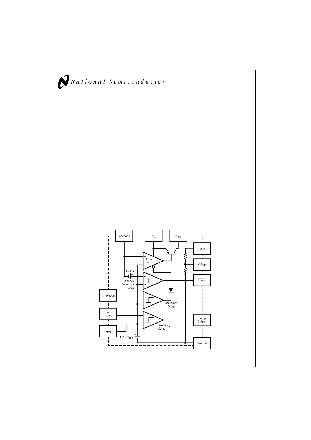
Block Diagram
DS011962-1
April 1999
LP2960 Adjustable Micropower 0.5A Low-Dropout Regulators
© 1999 National Semiconductor Corporation DS011962 www.national.com
Absolute Maximum Ratings (Note 1)
If Military/Aerospace specified devices are required,
please contact the National Semiconductor Sales Office/
Distributors for availability and specifications.
Storage Temperature Range −65˚C to +150˚C
Operating Junction Temperature
Range
LP2960AI/LP2960I −40˚C to +125˚C
Lead Temperature (Soldering, 5 sec.) 260˚C
Power Dissipation (Note 2) Internally Limited
Input Supply Voltage −20V to +30V
Feedback Input Voltage (Note 3) −0.3V to +5V
Comparator Input Voltage (Note 4) −0.3V to +30V
Comparator Output Voltage (Note 4) −0.3V to +30V
ESD Rating (Note 15) 1.5 kV
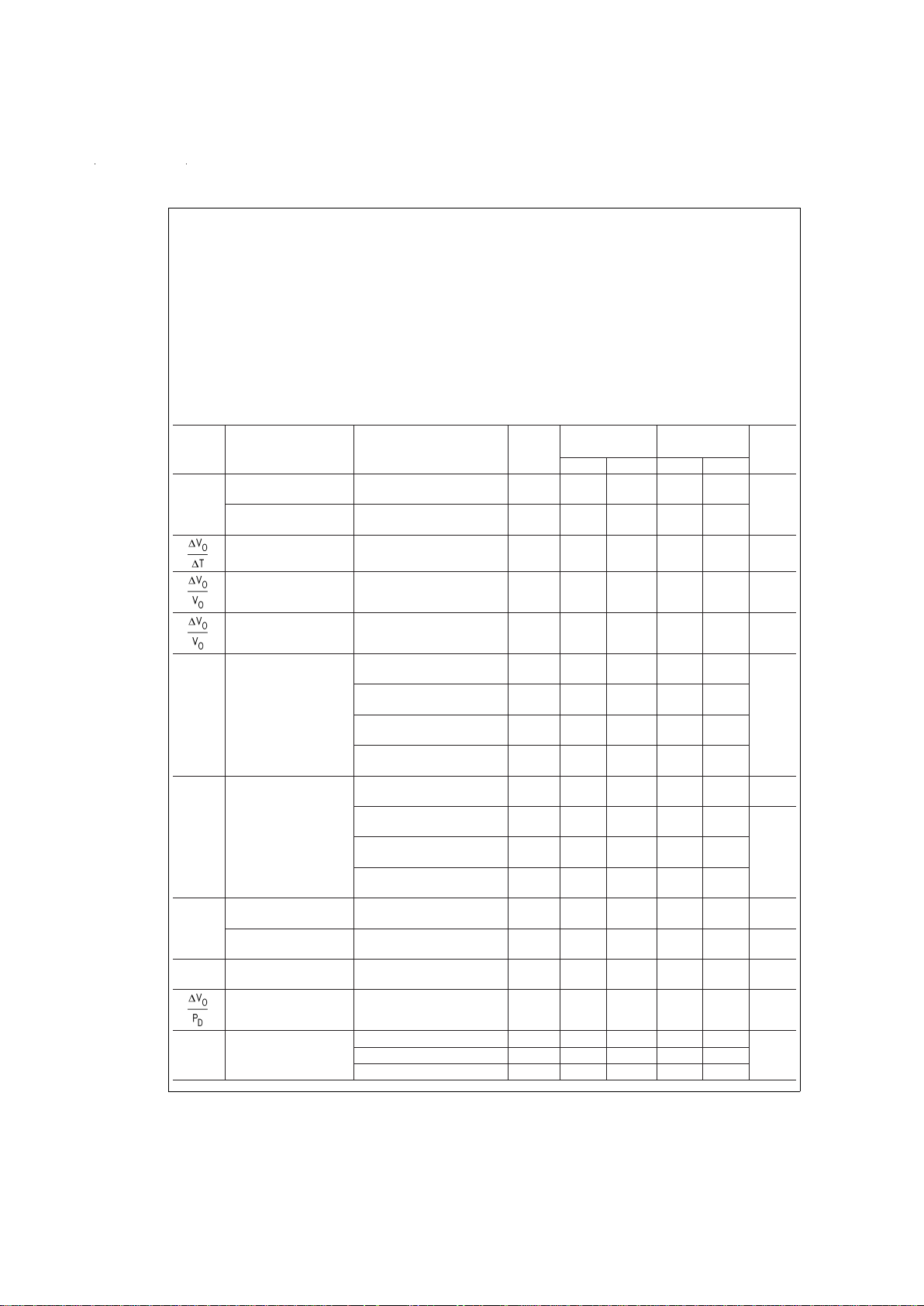
Electrical Characteristics Limits in standard typeface are for T
J
=
25˚C, and limits in boldface type apply
over the full operating temperature range. Unless otherwise specified: C
IN
=
4.7 µF, V
IN
=
V
O
(NOM) + 1V, I
L
=
1 mA,
C
OUT
=
10 µF for 5V parts or C
OUT
=
22 µF for 3.3V parts, Feedback pin is tied to V
TAP
pin, Output pin is tied to Sense pin,
V
S/D
=
2V.
Symbol Parameter Conditions Typ
LP2960AI
(Note 14)
LP2960I
(Note 14)
Units
Min Max Min Max
V
O
Output Voltage
(5V Versions)
1mA≤IL≤500 mA
5.0
4.962
4.930
5.038
5.070
4.925
4.880
5.075
5.120
V
Output Voltage
(3.3 Versions)
1mA≤I
L
≤500 mA
3.3
3.275
3.254
3.325
3.346
3.250
3.221
3.350
3.379
Output Voltage
Temperature Coefficient
(Note 5)
20 130 160 ppm/˚C
Output Voltage
Line Regulation
V
IN
=
[V
O
(NOM) + 1V] to 30V
0.06
0.2
0.5
0.4
0.8
%
Output Voltage
Load Regulation
(Note 6)
0.08
0.16
0.30
0.20
0.40
%
V
IN−VO
Dropout Voltage (Note 7) I
L
=
1mA
12
30
50
30
50
mV
I
L
=
100 mA
180
250
350
250
350
I
L
=
200 mA
260
350
450
350
450
I
L
=
500 mA
470
600
800
600
800
I
GND
Ground Pin Current
(Note 8)
I
L
=
1mA
450
600
750
600
750
µA
I
L
=
100 mA
2.6
4.0
5.0
4.0
5.0
mA
I
L
=
200 mA
2.5
8
10
8
10
I
L
=
500 mA
21
35
40
35
40
I
GND
Ground Pin Current
at Dropout (Note 8)
V
IN
=
V
O
(NOM) − 0.5V
I
L
=
100 µA
1.8
3
5
3
5
mA
Ground Pin Current
at Shutdown (Note 8)
V
SD
≤ 1.1V
300 400 400 µA
I
LIMIT
Current Limit R
L
=
0.5Ω
1000
1500
1600
1500
1600
mA
Thermal Regulation (Note 10)
0.05 0.2 0.2
%
/W
e
n
Output Noise Voltage
@
I
L
=
100 mA
(10 Hz–100kHz)
C
OUT
=
10 µF 300
µV RMSC
OUT
=
47 µF 210
C
OUT
=
47 µF (Note 11) 130
www.national.com 2
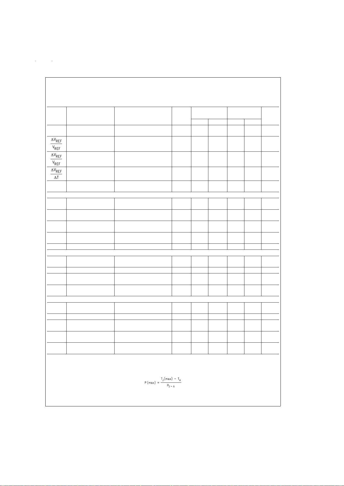
Electrical Characteristics Limits in standard typeface are for T
J
=
25˚C, and limits in boldface type apply
over the full operating temperature range. Unless otherwise specified: C
IN
=
4.7 µF, V
IN
=
V
O
(NOM) + 1V, I
L
=
1 mA,
C
OUT
=
10 µF for 5V parts or C
OUT
=
22 µF for 3.3V parts, Feedback pin is tied to V
TAP
pin, Output pin is tied to Sense pin,
V
S/D
=
2V. (Continued)
Symbol Parameter Conditions Typ
LP2960AI
(Note 14)
LP2960I
(Note 14)
Units
Min Max Min Max
V
REF
Reference Voltage
1.235
1.220
1.210
1.250
1.265
1.210
1.195
1.260
1.275
V
Reference Voltage
Line Regulation
(Note 13)
0.05
0.1
0.30
0.2
0.4
%
Reference Voltage
Load Regulation
I
REF
=
0–200 µA
0.45
0.6
0.9
1.2
1.5
%
Reference Voltage
Temperature Coefficient
(Note 5)
20 ppm/˚C
I
B
(FB) Feedback Pin Bias
Current
−20
−50
−70
−50
−70
nA
DROPOUT DETECTION COMPARATOR
I
OH
Output HIGH Leakage V
OH
=
30V
0.01
1
2
1
2
µA
V
OL
Output LOW Voltage V
IN
=
V
O
(NOM) − 1V
I
O
(COMP)=400 µA
125
250
400
250
400
mV
V
THR
(max) Upper Threshold Voltage (Note 9)
−60
−80
−100
−35
−25
−80
−100
−35
−25
mV
V
THR
(min) Lower Threshold Voltage (Note 9)
−85
−130
−200
−70
−35
−130
−200
−70
−35
mV
HYST Hysteresis (Note 9) 25 mV
SHUTDOWN INPUT
V
OS
Input Offset Voltage (Referred to V
REF
)
±
5
−18
−24
18
24
−18
−24
18
24
mV
HYST Hysteresis (Referred to V
REF
)10 mV
I
B
Input Bias Current V
S/D
=
0–5V
−20
−60
−10060100
−60
−10060100
nA
I
OUT
(S/D) Regulator Output Current
in Shutdown
(Note 12)
3
12
20
12
20
µA
AUXILIARY COMPARATOR
V
OS
Input Offset Voltage (Referred to V
REF
)
±
5
−15
−20
15
20
−15
−20
15
20
mV
HYST Hysteresis (Referred to V
REF
)10 mV
I
B
Input Bias Current V
COMP
=
0–5V
−20
−60
−10060100
−60
−10060100
nA
I
OH
Output HIGH Leakage V
OH
=
30V
V
COMP
=
1.3V
0.01
1
2
1
2
µA
V
OL
Output LOW Voltage V
COMP
=
1.1V
I
O
=
400 µA
125
250
400
250
400
mV
Note 1: Absolute maximum ratings indicate limits beyond which damage to the component may occur. Electrical specifications do not apply when operating the device outside of its rated operating conditions.
Note 2: The maximum allowable power dissipation is a function of the maximum junction temperature, T
J
(max), the junction-to-ambient thermal resistance, θ
J−A
,
and the ambient temperature, T
A
. The maximum allowable power dissipation at any ambient temperature is calculated using:
Exceeding the maximum allowable power dissipation will cause excessive die temperature, and the regulator will go into thermal shutdown. See APPLICATION
HINTS for additional information on heatsinking and thermal resistance.
Note 3: When used in dual-supply systems where the regulator load is returned to a negative supply, the output voltage must be diode-clamped to ground.
www.national.com3

Electrical Characteristics Limits in standard typeface are for T
J
=
25˚C, and limits in boldface type apply
over the full operating temperature range. Unless otherwise specified: C
IN
=
4.7 µF, V
IN
=
V
O
(NOM) + 1V, I
L
=
1 mA,
C
OUT
=
10 µF for 5V parts or C
OUT
=
22 µF for 3.3V parts, Feedback pin is tied to V
TAP
pin, Output pin is tied to Sense pin,
V
S/D
=
2V. (Continued)
Note 4: May exceed the input supply voltage.
Note 5: Output or reference voltage temperature coefficient is defined as the worst case voltage change divided by the total temperature range.
Note 6: Output voltage load regulation is measured at constant junction temperature using low duty cycle pulse testing. Two separate tests are performed, one for
the load current range of 100 µA to 1 mA and one for the 1 mA to 500 mA range. Changes in output voltage due to heating effects are covered by the thermal regulation specification.
Note 7: Dropout voltage is defined as the input to output differential at which the output voltage drops 100 mV below the value measured with a 1V differential. At
very low values of programmed output voltage, the input voltage minimum of 2V (2.3V over temperature) must be observed.
Note 8: Ground pin current is the regulator quiescent current. The total current drawn from the source is the sum of the ground pin current, output load current, and
current through the external resistive divider (if used).
Note 9: Dropout detection comparator threshold voltages are expressed in terms of a voltage differential measured at the Feedback terminal below the
nominal
ref-
erence voltage, which is the reference voltage measured with V
IN
=
V
O
(NOM) + 1V.To express these thresholds in terms of output voltage change, multiply by the
error amplifier gain which is V
O/VREF
=
(R1 + R2)/R2 (see
Basic Application Circuit
).
Note 10: Thermal regulation is the change in output voltage at a time T after a change in power dissipation, excluding load or line regulation effects. Specifications
are for a 400 mA load pulse at V
IN
=
V
O
(NOM) + 15V (6W pulse) for T=10 ms.
Note 11: Connect a 0.1 µF capacitor from the output to the feedback pin.
Note 12: Vshutdown ≤ 1.1V, V
IN
<
30V, V
OUT
=
0V.
Note 13: Two separate tests are performed for referenc e voltage line regulation, one covering 2.5V ≤ V
IN
≤ VO(NOM) + 1V and the other test for VO(NOM) + 1V
≤ V
IN
≤ 30V.
Note 14: All room temperature limits are 100%production tested.Alllimitsattemperature extremes are guaranteed via correlation using standard Statistical Quality
Control (SQC) methods. All limits are used to calculate Average Outgoing Quality Level.
Note 15: Human Body Model, 200 pF discharged through 1.5 kΩ.
www.national.com 4
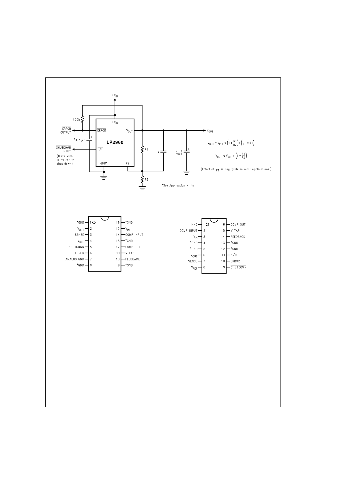
Basic Application Circuit
Connection Diagrams and Ordering Information
DS011962-2
16-Pin Surface Mount Package
DS011962-3
Top View
Order Number LP2960IM-5.0, LP2960AIM-5.0,
LP2960IM-3.3 or LP2960AIM-3.3
See NS Package Number M16A
16-Pin DIP Package
DS011962-4
Top View
Order Number LP2960IN-5.0, LP2960AIN-5.0,
LP2960IN-3.3 or LP2960AIN-3.3
See NS Package Number N16G
*
Internally Connected to Power Ground
www.national.com5
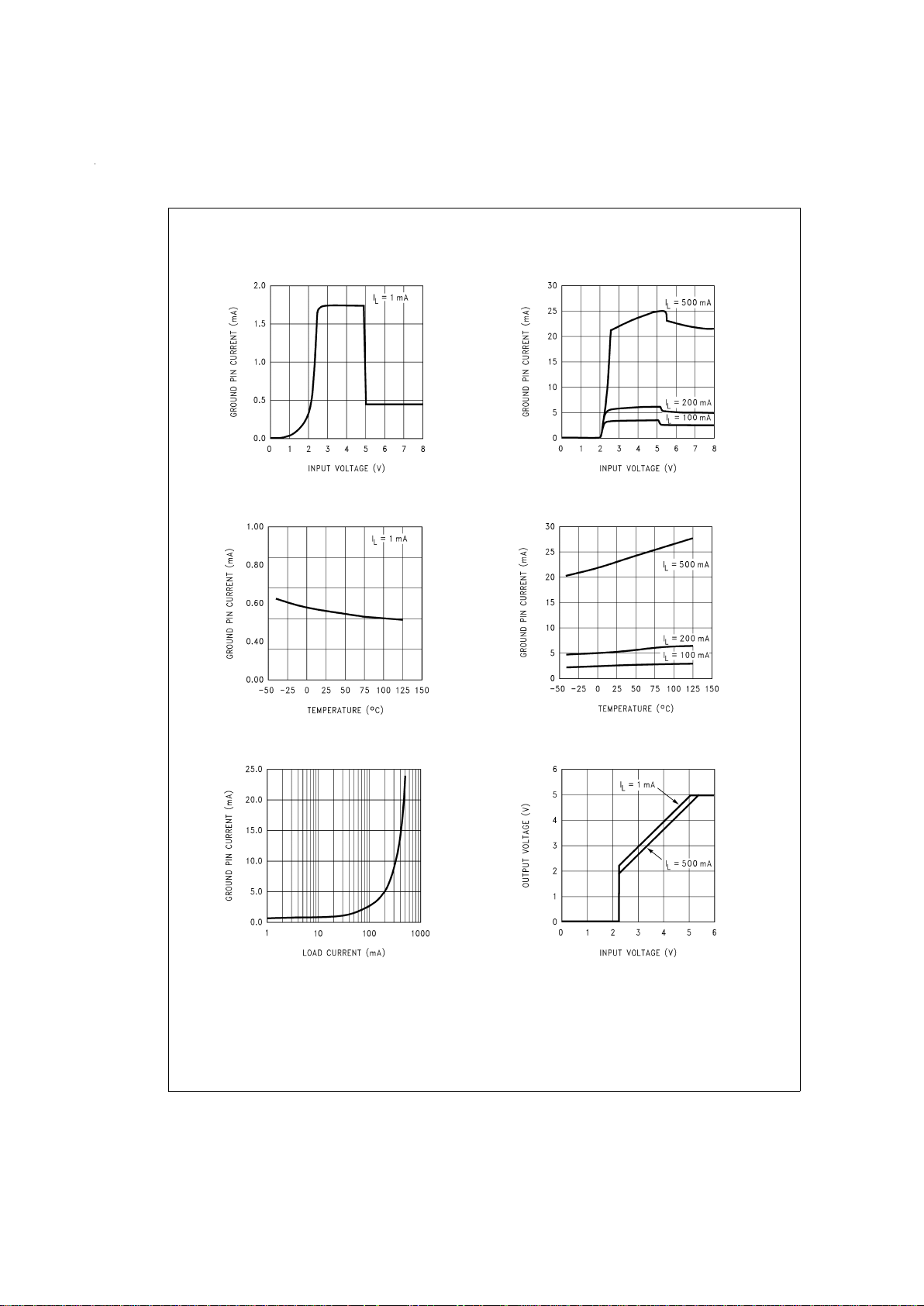
Typical Performance Characteristics Unless otherwise specified: C
IN
=
4.7 µF, V
IN
=
6V, I
L
=
1 mA,
C
OUT
=
10 µF, Feedback pin is tied to V
TAP
pin, Output pin is tied to Sense pin, V
S/D
=
2V, V
OUT
=
5V.
Ground Pin Current
DS011962-5
Ground Pin Current
DS011962-6
Ground Pin Current
DS011962-7
Ground Pin Current
DS011962-8
Ground Pin Current
DS011962-9
Dropout Characteristics
DS011962-10
www.national.com 6
 Loading...