NSC LP2956IN, LP2956IMX, LP2956IM, LP2956AIMX, LP2956AIM Datasheet
...
LP2956/LP2956A
Dual Micropower Low-Dropout Voltage Regulators
General Description
The LP2956 is a micropower voltage regulator with very low
quiescent current (170 µAtypical at light loads) and very low
dropout voltage (typically 60 mV at 1 mA load current and
470 mV at 250 mA load current on the main output).
The LP2956 retains all the desirable characteristics of the
LP2951, but offers increased output current (main output),
an auxiliary LDO adjustable regulated output (75 mA), and
additional features.
The auxiliary output is always on (regardless of main output
status), so it can be used to power memory circuits.
Quiescent current increases only slightly at dropout, which
prolongs battery life.
The error flag goes low if the main output voltage drops out
of regulation.
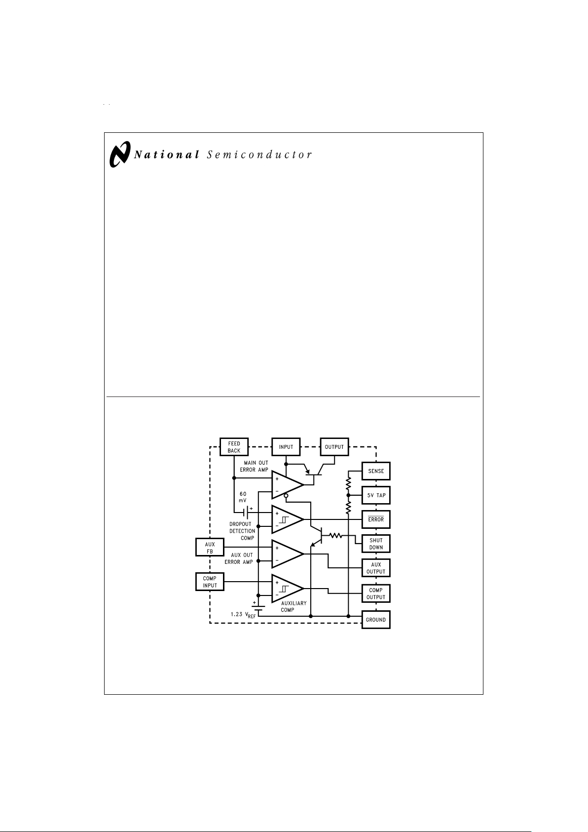
An open-collector auxiliary comparator is included, whose inverting input is tied to the 1.23V reference.
Reverse battery protection is provided.
The parts are available in DIP and surface mount packages.
Features
n Output voltage adjusts from 1.23V to 29V
n Guaranteed 250 mA current (main output)
n Auxiliary LDO (75 mA) adjustable output
n Auxiliary comparator with open-collector output
n Shutdown pin for main output
n Extremely low quiescent current
n Low dropout voltage
n Extremely tight line and load regulation
n Very low temperature coefficient
n Current and thermal limiting
n Reverse battery protection
Applications
n High-efficiency linear regulator
n Low dropout battery-powered regulator
n µP system regulator with switchable high-current V
CC
Block Diagram
LP2956
DS011339-1
May 1999
LP2956/LP2956A Dual Micropower Low-Dropout Voltage Regulators
© 1999 National Semiconductor Corporation DS011339 www.national.com
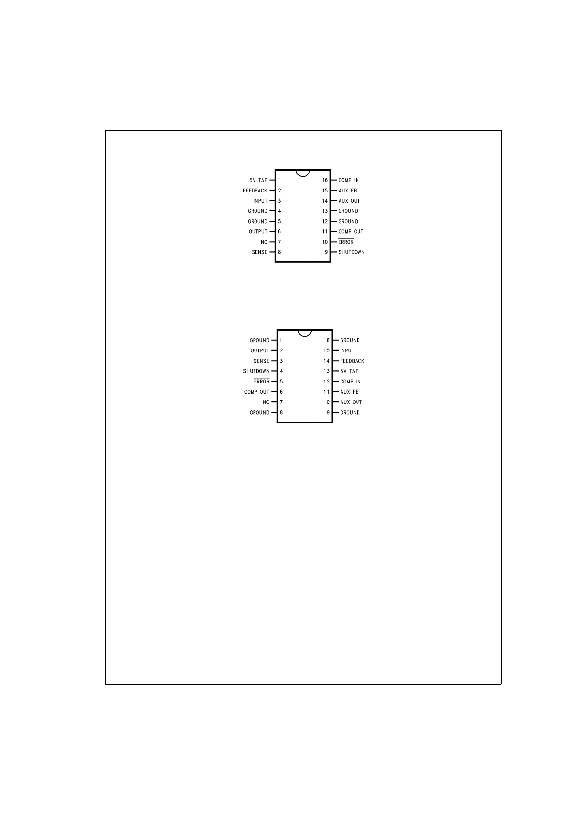
Connection Diagrams
16–Pin DIP
DS011339-2
Order Number LP2956IN or LP2956AIN
See NS Package Number N16A
Order Number LP2956AMJ-QML or 5962-9554701QEA
See NS Package Number J16A
16-Pin Surface Mount
DS011339-3
Order Number LP2956IM or LP2956AIM
See NS Package Number M16A
www.national.com 2
Absolute Maximum Ratings (Note 1)
If Military/Aerospace specified devices are required,
please contact the National Semiconductor Sales Office/
Distributors for availability and specifications.
Storage Temperature Range −65˚C to +150˚C
Operating Junction
Temperature Range −40˚C to +125˚C
Lead Temperature
(Soldering, 5 seconds) 260˚C
Power Dissipation (Note 2) Internally Limited
Input Supply Voltage −20V to +30V
Feedback Input Voltage (Note 3) −0.3V to +5V
Aux. Feedback Input Voltage (Note 3) −0.3V to +5V
Shutdown Input Voltage (Note 3) −0.3V to +30V
Comparator Input Voltage (Notes 3,
4) −0.3V to +30V
Comparator Output Voltage (Notes 3,
4) −0.3V to +30V
ESD Rating (Note 16) 2 kV
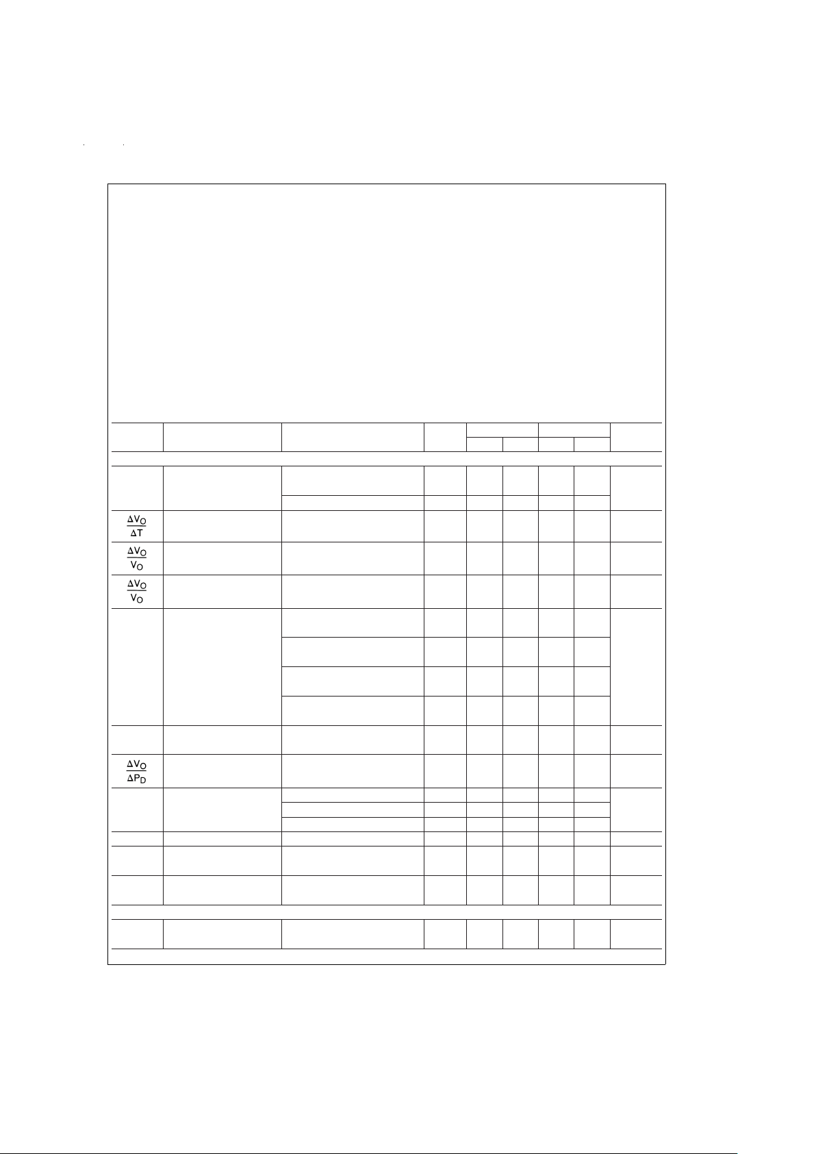
Electrical Characteristics
Limits in standard typeface are for T
J
=
25˚C, and limits in boldface type apply over the full operating temperature range. Limits are guaranteed by production testing or correlation techniques using standard Statistical Quality Control (SQC) methods.
Unless otherwise specified: V
IN
=
6V, C
L
=
2.2 µF (Main Output) and 10 µF (Auxiliary Output), Feedback pin is tied to 5V Tap
pin, C
IN
=
1 µF, V
SD
=
0V, Main Output pin is tied to Output Sense pin, Auxiliary Output is programmed for 5V. The main
regulator output hasa1mAload, the auxiliary regulator output has a 100 µA load.
Symbol Parameter Conditions Typical LP2956AI LP2956I Units
Min Max Min Max
MAIN OUTPUT
V
O
Output Voltage 5.0 4.975 5.025 4.950 5.050
4.940 5.060 4.900 5.100 V
1mA≤I
L
≤250 mA 5.0 4.930 5.070 4.880 5.120
Temperature Coefficient (Note 5) 20 100 150 ppm/˚C
Line Regulation V
IN
=
6V to 30V 0.03 0.1 0.2
%
0.2 0.4
Load Regulation I
L
=
1 mA to 250 mA 0.04 0.16 0.20
%
I
L
=
0.1 mA to 1 mA (Note 6) 0.20 0.30
V
IN–VO
Dropout Voltage I
L
=
1 mA 60 100 100
(Note 7) 150 150
I
L
=
50 mA 240 300 300
420 420 mV
I
L
=
100 mA 310 400 400
520 520
I
L
=
250 mA 470 600 600
800 800
I
LIMIT
Current Limit R
L
=
1Ω 380 500 500 mA
530 530
Thermal Regulation (Note 8) 0.05 0.2 0.2
%
/W
e
n
Output Noise Voltage C
L
=
2.2 µF 400
(10 Hz to 100 KHz) C
L
=
33 µF 260 µV RMS
I
L
=
100 mA C
L
=
33 µF (Note 9) 80
V
FB
Feedback Pin Voltage 1.23 1.215 1.245 1.205 1.255 V
I
FB
Feedback Pin Bias 20 40 40 nA
Current 60 60
I
O
Output Leakage I
(SD IN)
≥ 1 µA 3 10 10 µA
(OFF) In Shutdown V
IN
=
30V, V
OUT
=
0V 20 20
AUXILIARY OUTPUT
V
FB
Feedback Pin Voltage 1.23 1.22 1.25 1.21 1.26 V
1.21 1.26 1.20 1.27
www.national.com3
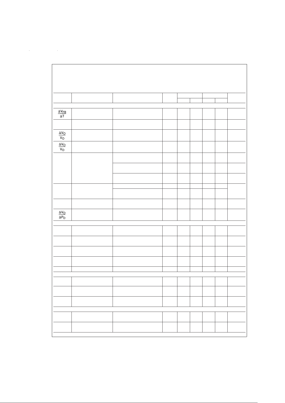
Electrical Characteristics (Continued)
Limits in standard typeface are for T
J
=
25˚C, and limits in boldface type apply over the full operating temperature range. Limits are guaranteed by production testing or correlation techniques using standard Statistical Quality Control (SQC) methods.
Unless otherwise specified: V
IN
=
6V, C
L
=
2.2 µF (Main Output) and 10 µF (Auxiliary Output), Feedback pin is tied to 5V Tap
pin, C
IN
=
1 µF, V
SD
=
0V, Main Output pin is tied to Output Sense pin, Auxiliary Output is programmed for 5V. The main
regulator output hasa1mAload, the auxiliary regulator output has a 100 µA load.
Symbol Parameter Conditions Typical LP2956AI LP2956I Units
Min Max Min Max
AUXILIARY OUTPUT
Feedback Voltage
Temperature Coefficient
20 ppm/˚C
I
FB
Feedback Pin Bias 10 20 20 nA
Current 30 30
Line Regulation 6V ≤ VIN≤ 30V 0.07 0.3 0.4
%
0.5 0.6
Load Regulation I
L
=
0.1 mA to 1 mA 0.1 0.3 0.4
%
I
L
=
1 mA to 75 mA (Note 10) 0.6 1.0
V
IN–VO
Dropout Voltage I
L
=
1 mA 100 200 200 mV
300 300
I
L
=
50 mA 400 600 600 mV
700 700
I
L
=
75 mA 500 700 700 mV
850 850
e
n
Output Noise C
L
=
10 µF 300
(10 Hz–100 KHz) C
L
=
33 µF (Note 9) 100 µV RMS
I
L
=
10 mA
I
LIM
Current Limit V
OUT
=
0V (Note 13) 80 200 200 mA
250 250
Thermal Regulation (Note 8) 0.2 0.5 0.5
%
/W
DROPOUT DETECTION COMPARATOR
I
OH
Output “HIGH” Leakage V
OH
=
30V 0.01 1 1 µA
22
V
OL
Output “LOW” Voltage V
IN
=
4V 150 250 250 mV
I
O
(COMP)=400 µA 400 400
V
THR
Upper Threshold Voltage (Note 11) −240 −320 −150 −320 −150 mV
(max) −380 −100 −380 −100
V
THR
Lower Threshold Voltage (Note 11) −350 −450 −230 −450 −230 mV
(min) −640 −160 −640 −160
HYST Hysteresis (Note 11) 110 mV
SHUTDOWN INPUT
I
IN
Input Current to Disable
Output
(Note 12) 0.03 0.5 0.5 µA
V
IH
Shutdown Input High I
(SD IN)
≥ 1 µA 900 900 mV
Threshold 1200 1200
V
IL
Shutdown Input Low VO≥ 4.5V 400 400 mV
Threshold 200 200
AUXILIARY COMPARATOR
V
T
(high) Upper Trip Point (Note 14) 1.236 1.20 1.28 1.20 1.28 V
1.19 1.29 1.19 1.29
V
T
(low) Lower Trip Point (Note 14) 1.230 1.19 1.27 1.19 1.27 V
1.18 1.28 1.18 1.28
www.national.com 4
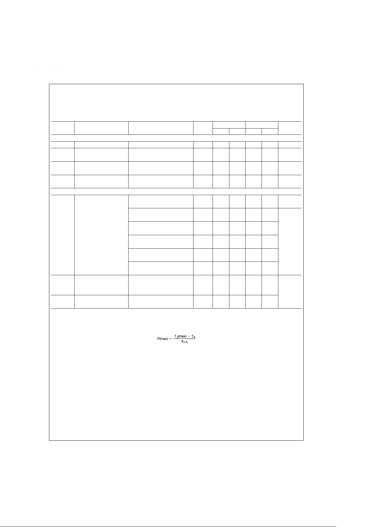
Electrical Characteristics (Continued)
Limits in standard typeface are for T
J
=
25˚C, and limits in boldface type apply over the full operating temperature range. Limits are guaranteed by production testing or correlation techniques using standard Statistical Quality Control (SQC) methods.
Unless otherwise specified: V
IN
=
6V, C
L
=
2.2 µF (Main Output) and 10 µF (Auxiliary Output), Feedback pin is tied to 5V Tap
pin, C
IN
=
1 µF, V
SD
=
0V, Main Output pin is tied to Output Sense pin, Auxiliary Output is programmed for 5V. The main
regulator output hasa1mAload, the auxiliary regulator output has a 100 µA load.
Symbol Parameter Conditions Typical LP2956AI LP2956I Units
Min Max Min Max
AUXILIARY COMPARATOR
HYST Hysteresis 6 mV
I
OH
Output “HIGH” Leakage V
OH
=
30V 0.01 1 1 µA
V
IN
(COMP)=1.3V 22
V
OL
Output “LOW” Voltage VIN(COMP)=1.1V 150 250 250 mV
I
O
(COMP)=400 µA 400 400
I
B
Input Bias Current 0 ≤ VIN(COMP) ≤ 5V 10 −30 30 −30 30 nA
−50 50 −50 50
GROUND PIN CURRENT
I
GND
Ground Pin Current IL(Main Out)=1 mA 170 250 250 µA
(Note 15) I
L
(Aux. Out)=0.1 mA 280 280
I
L
(Main Out)=50 mA 1.1 2 2
I
L
(Aux. Out)=1mA 2.5 2.5
I
L
(Main Out)=100 mA 3 6 6
I
L
(Aux. Out)=1mA 88
I
L
(Main Out)=250 mA 16 28 28 mA
I
L
(Aux. Out)=1mA 33 33
I
L
(Main Out)=1mA 3 6 6
I
L
(Aux. Out)=50 mA 88
I
L
(Main Out)=1mA 6 8 8
I
L
(Aux. Out)=75 mA 10 10
I
GND
Ground Pin Current V
IN
=
4.5V 325 325
at Dropout (Note 15) I
L
(Main Out)=0.1 mA 270 350 350
I
L
(Aux. Out)=0.1 mA µA
I
GND
Ground Pin Current No Load on Either Output 120 180 180
at Shutdown (Note 15) I
(SD IN
) ≥ 1µA 200 200
Note 1: Absolute maximum ratings indicate limits beyond which damage to the component may occur. Electrical specifications do not apply when operating the device outside of its rated operating conditions.
Note 2: The maximum allowable power dissipation is a function of the maximum junction temperature, T
J
(max), the junction-to-ambient thermal resistance, θ
J-A
,
and the ambient temperature, T
A
. The maximum allowable power dissipation at any ambient temperature is calculated using: P(max)
=
.
Exceeding the maximum allowable power dissipation will cause excessive die temperature, and the regulator will go into thermal shutdown. SeeApplication Hints for
additional information on heat sinking and thermal resistance.
Note 3: When used in dual-supply systems where the regulator load is returned to a negative supply, the output voltage must be diode-clamped to ground.
Note 4: May exceed the input supply voltage.
Note 5: Output or reference voltage temperature coefficient is defined as the worst case voltage change divided by the total temperature range.
Note 6: Load regulation is measured at constant junction temperature using low duty cycle pulse testing. Twoseparate tests are performed, one for the range of 100
µA to 1 mA and one for the 1 mA to 250 mA range. Changes in output voltage due to heating effects are covered by the thermal regulation specification.
Note 7: Dropout voltage is defined as the input to output differential at which the output voltage drops 100 mV below the value measured with a 1V differential. At
very low values of programmed output voltage, the input voltage minimum of 2V (2.3V over temperature) must be observed.
Note 8: Thermal regulation is the change in output voltage at a time T after a change in power dissipation, excluding load or line regulation effects. Specifications
are for a 200 mA load pulse at V
IN
=
20V (3W pulse) for T=10 ms on the Main regulator output. For the Auxiliary regulator output, specifications are for a 66 mA
load pulse at V
IN
=
20V (1W pulse) for T=10 ms.
Note 9: Connect a 0.1 µF capacitor from the output to the feedback pin.
Note 10: Load regulation is measured at constant junction temperature using low duty cycle pulse testing. Two separate tests are performed, one for the range of
100 µA to 1 mA and one for the 1 mA to 75 mA range. Changes in output voltage due to heating effects are covered by the thermal regulation specification.
Note 11: Dropout dectection comparator thresholds are expressed as changes in a 5V output. To express the threshold voltages in terms of a differential at the
Feedback terminal, divide by the error amplifier gain=V
OUT/VREF
.
www.national.com5
 Loading...